EP0347929B1 - Parallel processor - Google Patents
Parallel processor Download PDFInfo
- Publication number
- EP0347929B1 EP0347929B1 EP89111465A EP89111465A EP0347929B1 EP 0347929 B1 EP0347929 B1 EP 0347929B1 EP 89111465 A EP89111465 A EP 89111465A EP 89111465 A EP89111465 A EP 89111465A EP 0347929 B1 EP0347929 B1 EP 0347929B1
- Authority
- EP
- European Patent Office
- Prior art keywords
- bus
- processing units
- data
- input
- mppe
- Prior art date
- Legal status (The legal status is an assumption and is not a legal conclusion. Google has not performed a legal analysis and makes no representation as to the accuracy of the status listed.)
- Expired - Lifetime
Links
Images


Classifications
-
- G—PHYSICS
- G06—COMPUTING; CALCULATING OR COUNTING
- G06F—ELECTRIC DIGITAL DATA PROCESSING
- G06F15/00—Digital computers in general; Data processing equipment in general
- G06F15/16—Combinations of two or more digital computers each having at least an arithmetic unit, a program unit and a register, e.g. for a simultaneous processing of several programs
-
- G—PHYSICS
- G06—COMPUTING; CALCULATING OR COUNTING
- G06F—ELECTRIC DIGITAL DATA PROCESSING
- G06F13/00—Interconnection of, or transfer of information or other signals between, memories, input/output devices or central processing units
- G06F13/38—Information transfer, e.g. on bus
- G06F13/40—Bus structure
- G06F13/4004—Coupling between buses
- G06F13/4022—Coupling between buses using switching circuits, e.g. switching matrix, connection or expansion network
-
- G—PHYSICS
- G06—COMPUTING; CALCULATING OR COUNTING
- G06F—ELECTRIC DIGITAL DATA PROCESSING
- G06F15/00—Digital computers in general; Data processing equipment in general
- G06F15/16—Combinations of two or more digital computers each having at least an arithmetic unit, a program unit and a register, e.g. for a simultaneous processing of several programs
- G06F15/163—Interprocessor communication
- G06F15/173—Interprocessor communication using an interconnection network, e.g. matrix, shuffle, pyramid, star, snowflake
- G06F15/17337—Direct connection machines, e.g. completely connected computers, point to point communication networks
- G06F15/17343—Direct connection machines, e.g. completely connected computers, point to point communication networks wherein the interconnection is dynamically configurable, e.g. having loosely coupled nearest neighbor architecture
Definitions
- the present invention relates to a parallel processor according to the preamble portion of claim 1, and more particularly to a parallel processor suitably used for a graphic job.
- a plurality of processors include, for example, a CPU and a local memory being connected to a common bus, wherein a CPU in a certain processor performs writing and reading a local memory in the other processor through the common bus.
- Another system which includes a plurality of common buses and transference of data between processors are individually performed.
- a still further known system is arranged such that a plurality of processors are connected annularly, in the form of a lattice, or a binary tree.
- a system is known which is arranged in such a manner that communication is performed between processors connected vertically and laterally, so that a so-called "CAP (Cellular Array Processor)" is formed.
- CAP Cellular Array Processor
- EP-A-225 022 shows a multi-node data processing system with a central switch or a star coupler which is connected to each node by means of separate paths in order to provide an improved way of interconnecting the nodes, which does not suffer from the failure of the whole system, if the central switch or the star coupler fails.
- the nodes are provided with switching units, which can be selected so that each of the switching units can act as a star coupler for receiving messages from any of the nodes and broadcasting each message to all the nodes.
- An object of the present invention is to provide a parallel processor in which the connections between a plurality of processors can be re-structured in accordance with the processing algorithm and various processings can be performed at high speed by means of a parallel operation.
- the parallel processor includes a plurality of processing units connected to each other via input/output ports.
- Each of the plurality of processing units comprises a memory for storing programs and data, a local bus for inputting/outputting the program and data to and from the memory and consisting of an address signal line, a data signal line, and a control signal line, a CPU for reading the program from the memory via the local bus as to process the program, for reading data needed to perform the processing from the memory via the local bus, and for making data which have been updated due to the processing to be stored again by the memory via the local bus, a plurality of input/output ports capable of connecting the local bus to a plurality of outside buses and needed for the CPU to input/output data to and from an outside memory other than the memory or for an outer CPU to input/output data to and from the memory, and bus switches for connecting two of the outside buses for the purpose of enabling data transference between the CPU and the memory which are disposed on individual buses to be performed, wherein a main CPU for setting program and
- Fig. 1 is a view which illustrates an example of a parallel processor according to the present invention.
- a CPU 10, a DMAC 11, and a system memory 12 are respectively connected to a common bus line 100.
- Four multiport processing elements (to be called “MPPEs” hereinafter) 13 connected in series to each other are connected to this bus line 100.
- a frame buffer 15 is connected to an MPPE 13 which is disposed rearmost of the configuration of the four MPPEs 13.
- a CRT display 16 is connected to an end of this frame buffer 15, while a display control unit 14 is connected to another end of the same.
- the above-described MPPE 13 comprises two input/output ports as to be used with its ports connected to corresponding ports of another MPPE 13 of the same type.
- the number of the MPPEs is not limited. Although the number of the input/output ports of the MPPE 13 is determined to be two with reference to the drawing, the number of the input/output ports can also be optionally determined.
- a CPU 130 and a local memory 131 are connected to the common bus, and input/output ports 132 are respectively connected to this common bus at positions outside the corresponding intersections of the CPU 130 and the local memory 131.
- a bus switch 133 enabling the outsides of the input/output ports 132 to be connected to each other is included in the MPPE 13.
- the above-described CPU 130 performs a predetermined processing in accordance with a program stored in the local memory 131. Data which has been processed is stored in the local memory 131. In a case where it is impossible for a single MPPE 13 to complete the processing, the other MPPE 13 is accessed via the input/output port 132.
- the structure is so arranged that addresses, data, and control signals can be transported between the ports of the MPPEs 13. That is, the MPPE 13 can access the local memory 131 or consign the processing to the other CPU 130 of the other MPPE 13.
- the bus switches 133 in the MPPEs 13 are provided for the purpose of controlling the connections between the input/output ports 132.
- a fact whether this switch 133 is opened or closed is arranged to be determined on the basis of a value of the register in the bus switch 133. This value is determined by way of assignment of the register number performed by the CPU 130 on the basis of the program to be determined by the CPU 10 and processed by the MPPE 13.
- the MPPE 13 is accessed from outside and the bus switch 133 is closed, information obtained from the input/output port 132 is supplied from the other input/output port to the other MPPE 13 via the bus switch 133.
- Picture element data which has been processed by the MPPE 13 is stored in a frame buffer 15. The data stored in the frame buffer 15 is read by the display control unit 14 so that an image is displayed on the above-described CRT display 16.
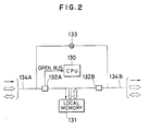
- Fig. 2 is a view which illustrates an access from outside to the local memory in the above-described MPPE 13.
- the control information, address, and data are input through an input/output port 132A.
- the bus switch 133 When the bus switch 133 is set to be closed, the information above is immediately transferred to the other MPPE 13 connected to another input/output port 132B through this input/output port 132B.
- the input/output port 132A decodes the control information and the address which have been input to the input/output port 134A.
- the input/output port 132A issues a demand to the CPU 130 to open the bus.
- the CPU 130 opens the bus and as well acknowledge the input/output port 132A a fact that the bus has been opened.
- the input/output port 132A transfers the control information, address, and data to be input through the input/output port 134 to the local memory 131.
- the input/output port 132B demands the CPU 130 to open the bus so that the control information, address, and data to be input through the input/output port 134B are transferred to the local memory 131.
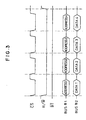
- Fig. 3 is a view which illustrates a time chart when an access to the local memory 131 of the MPPE 13 is performed, in which three types of control signals and two types of data are selected to be indicated from necessary signals for performing the access. These control signals and data are input through the input/output port 134A or 134B shown in Fig. 2, and are transferred to the local memory 131 through the input/output port 132A or 132B. Referring to Fig. 3, a control signal CS acts to realize a LOW level during a period in which data and address data are supplied to the local memory 131.
- a control signal R/W is a signal acting to distinguish whether data is read from the local memory or data is written in the same where the "HIGH” level means reading while the "LOW” level means writing.
- a control signal BT realizes a "LOW" level when data is simultaneously transferred from two types of buses BUS #1 and #2 to the local memory 131.
- the BUS #1 is used for address transference, while the bus #2 is used for data transference.
- the "message region” represents a memory region which is distinguished from the program data region by an address and which serves as means for storing an address in which the message transferred from the other MPPE 13 is written and the number of the messages are stored.
- a structure is formed such that the address of the access corresponding to the first word is assigned in response to an access from the message region, and a bus which is used for general address transference can be used for the data transference of the second word and ensuing words.
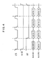
- Fig. 4 is a time chart which illustrates a mode in which two words are transferred between individual MPPEs 13 such that an address is assigned at the transference of the first word and the address bus is also used for the data transference from the second word and the ensuing word when CPU 10 transfers data of a plurality of words to the message region of the local memory 131.
- the address in the local memory 131 in a specific MPPE 13 is transferred through the BUS #1, and at the second and the ensuing accesses both the BUS #1 and # 2 are used to simultaneously transfer data for two words.
- the level of the control signal BT needs to be set to the LOW level.
- both the control signals CS and BT needs to be set to the HIGH level.
- Fig. 5 is a view which illustrates an action of writing in the local memory of the CPU between individual MPPEs which are directly connected to each other.
- This drawing illustrates a case where the CPU 130 in the MPPE 13A performs writing in the local memory 131 in the MPPE 13C.
- the bus switches 133 in the corresponding MPPEs 13A, 13B, and 13C are respectively programmed in the sequential order as OPEN, CLOSE, and OPEN.
- the control signal, address (BUS # 1 is used), and data (BUS #2 is used) transmitted by the MPPE 13A are transferred to the MPPEs 13B and 13Z which are to be connected to the MPPE 13A via the input/output ports 132A and 132B of the MPPE 13A.
- the bus switch 133 is set to CLOSE so that the control signal, address, and data transmitted from the input/output port 132B of the MPPE 13A are immediately transferred to the MPPE 13B.
- the description about the action within the MPPE 13Z is omitted here.
- the input/output port 132A in the MPPE 13B determines by using an address decoder included therein whether or not the subject access is an access to the local memory 131.
- the address includes both the processor address and the local memory address, and decodes the processor address. In this case, since it is not the access to the local memory 131 (in the MPPE 13B), the CPU 130 in the MPPE 13B can access the local memory 131.
- the input/output port 132A in the MPPE 13C determines, by using the address decoder provided therein, a fact that it is the access to the local memory 131 (MPPE 13C), and upon this determination the input/output port 132A in the MPPE 13C issues a demand toward the CPU 130 of the MPPE 13C for a bus.
- This CPU 130 issues a permission of use of the bus to the input/output port 132A (in the MPPE 13C) when the state in which the bus can be opened is realized.
- This input/output port 132A transfers the control signal, address, and data to the local memory 131 (in the MPPE 13C).
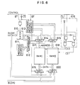
- Fig. 6 is a view which illustrates the structure of the local memory which enables writing and reading of data for two words by its single access.
- a storage devices RAM I 617 and RAM II 618 perform writing and reading of a single word (the same bit size as that of the BUS #1 and #20) by their single accesses.
- the RAM I 617 corresponds to even-number addresses (the lowermost bit of the address is 0), while the RAM II 618 corresponds to the odd-number addresses (the lowermost bit of the address is 1).
- the address on the BUS # 1 is held by a latch 610, and is selected by multiplexers 614 and 615 as to be supplied to the RAM I 617 and RAM II 618.
- the detection of the access to the program and data region is performed by a comparator 612.
- the address space in the message region is stored in the register 611.
- One word is accessed to the program and data region for one time, and a chip select circuit 616 selects either the RAM I 617 or RAM II 618 in accordance with the lowermost bit of the address.
- the data is supplied from the BUS #2 to the RAM I 617 and RAM II 618 via multiplexers 619 and 620.
- a message address generator 613 controls the address. Therefore, information for identifying one of a plurality of local memories and information expressing a message are of significant among the addresses generated by the outside MPPE.
- the messages are successively stored by one in the local memory starting from the front address.
- the message address generator 613 includes a register for storing an address to be supplied when writing of a message is performed from the outer MPPE and a register for storing the address of the most antiquated message which has not as yet be read by the CUP.
- a mode in which data for two words is transferred by one access is called a "block transference mode". This mode is distinguished from an access of one word for one access by making the control signal BT to be LOW level.
- the block transference mode when two words are successively transferred from an even address, the same address is supplied to the RAM I 617 and RAM II 618 via the multiplexers 614 and 615. Data is supplied from the BUS # 2 to the RAM I 617, and is supplied from the BUS # 1 to the RAM II 618.
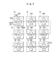
- Fig. 7 is a view which illustrates an embodiment in which 9 MPPEs are combined.
- the bus switches 133 of the corresponding MPPEs 13 can determine their state of opening and closing in accordance with a program. According to this embodiment, all are set to OPEN. Data and its control instruction are input from the input/output terminal 700 through the input/output port 132A. These data items are not transferred to the ensuing MPPE 13 since the bus switch 133 is opened. When the CPU 130 applies a processing to this data and makes the ensuing MPPE 13 to perform the next processing, data is transferred via the input/output port 132A.
- the data input through the input/output terminal 700 is subjected to a processing by means of the MPPE, that is, the 9 step pipe line processing, and is output from an input/output terminal 710.
- each MPPE receives data, applies a processing by an amount of one ninth, and supplies it to the next MPPE.
- data can be output from the final MPPE only taking one ninth of the time lapse.
- Fig. 8 is a view which illustrates another embodiment in which also 9 MPPEs are combined.
- the MPPE 13A, 13B, and 13C have a common terminal 800 arranged such that either of two input/output terminal thereof is connected to each other.
- the MPPE 13A is connected to a MPPE 13D by an input/output terminal, and is capable of being connected also to a MPPE 13G by setting a bus switch 133D in the MPPE 130 to be closed.
- MPPEs 13E and 13H are connected to the MPPE 13B, while MPPEs 13F and 13I are connected to the MPPE 13C.
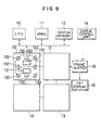
- Fig. 9 is a view which illustrates an embodiment in which four MPPEs each having four input/output ports are combined.
- the CPU 10, the DMAC 11, and the system memory 12 are connected to the common bus line 100, the MPPE 13 is connected to this bus line 100, a frame buffer 15 is connected to this MPPE 13, and the display device 14 and the CRT display 16 are connected to this frame buffer 15.
- the MPPEs are connected to the upper, lower, right and left (when viewed in Fig. 9) MPPEs via ports.
- the MPPE comprises: the CPU 130 and the local memory 131 connected to the common bus; two input/output ports 132 each of which is connected to this common bus at a position outside the intersection of the local memory 131 and the CPU 130; and the bus switches 133 which enable the connections between the ports.
- the CPUs 130 and the local memories 131 in the MPPEs can be connected to the upper, lower, right, and left MPPEs and as well be connected to the CPUs 130 and the local memories 131 in the neighboring MPPEs.
- the connections between CPUs can be changed even if the same system structure is employed.
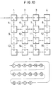
- Fig. 10 is a view which illustrates an embodiment in which the ports of 16 MPPEs are connected in the form of a 4 x 4 grating. All of the bus switches of the MPPEs are made open, and the same data is processed in the sequential order as 1, 5, 9, 13, 14, 10, 6, 7, 11, 15, 16, 12, 8, 4, 3, and 2. The data which has been processed in the MPPE 2 is returned to the MPPE 1.
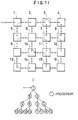
- Fig. 11 is a view which illustrates an embodiment in which another program is given to the bus switch of the embodiment shown in Fig. 10 so that the processors are connected to a four-layered binary tree.
- a plurality of MPPEs are connected to each other with the terminals thereof so that data and a signal expressing the state of opening and closing of the bus switch of the MPPEs 13 are supplied from the main CPU to one of the MPPEs. Therefore, the ports of the MPPEs 13 are arranged to include means for opening and closing the above-described bus switches in response to the input signal (signal expressing the state of opening and closing of the bus switch).
- the opening and closing of the bus switches of the MPPEs 13 may be arranged to be conducted in response to a signal representing an instruction to open/close the bus switches supplied directly from the main CPU (without passing though the ports).
- the opening and closing of the bus switches can be determined upon a comparison made between information stored in a register or the like provided in the bus switch and information about the signal representing an instruction to open/close the bus switches supplied from the main CPU by using this register or the like.
- the number of the ports provided for the MPPE 13 may be arranged to be two or more.
- a structure having four ports is provided with a first and a second data transference lines whose terminals are arranged to be the two ends of the signal lines such as bus lines and the like.
- a bus switch disposed between a terminal of the first data transference line and each terminal of the second data transference line, and between another terminal of the first data transference line and each terminal of the second data transference line; and an input/output port disposed to each end portions of the first and second data transference lines.
- the above-described bus switch and the input/output port have the same structure and the function as those above.
- connections of the processors can be re-structured in accordance with the processing algorithm, and various processings can be performed at high speed by means of a parallel operation.
Description
- The present invention relates to a parallel processor according to the preamble portion of
claim 1, and more particularly to a parallel processor suitably used for a graphic job. - In a prior art processor system a plurality of processors include, for example, a CPU and a local memory being connected to a common bus, wherein a CPU in a certain processor performs writing and reading a local memory in the other processor through the common bus.
- Another system is known which includes a plurality of common buses and transference of data between processors are individually performed. A still further known system is arranged such that a plurality of processors are connected annularly, in the form of a lattice, or a binary tree. In addition, a system is known which is arranged in such a manner that communication is performed between processors connected vertically and laterally, so that a so-called "CAP (Cellular Array Processor)" is formed.
- EP-A-225 022 shows a multi-node data processing system with a central switch or a star coupler which is connected to each node by means of separate paths in order to provide an improved way of interconnecting the nodes, which does not suffer from the failure of the whole system, if the central switch or the star coupler fails. The nodes are provided with switching units, which can be selected so that each of the switching units can act as a star coupler for receiving messages from any of the nodes and broadcasting each message to all the nodes.
- However, in any of the above-described processor system, the connection established between processors is fixed. Therefore, although specific processings can be performed at high speed, a problem arises in that it is difficult for the systems to correspond to the change in the algorithm, causing their use to be limited.
- An object of the present invention is to provide a parallel processor in which the connections between a plurality of processors can be re-structured in accordance with the processing algorithm and various processings can be performed at high speed by means of a parallel operation.
- The object is solved according to the features of
claim 1. The dependent claims show further embodiments and advantageous developments of the invention. - The parallel processor according to the present invention includes a plurality of processing units connected to each other via input/output ports. Each of the plurality of processing units comprises a memory for storing programs and data, a local bus for inputting/outputting the program and data to and from the memory and consisting of an address signal line, a data signal line, and a control signal line, a CPU for reading the program from the memory via the local bus as to process the program, for reading data needed to perform the processing from the memory via the local bus, and for making data which have been updated due to the processing to be stored again by the memory via the local bus, a plurality of input/output ports capable of connecting the local bus to a plurality of outside buses and needed for the CPU to input/output data to and from an outside memory other than the memory or for an outer CPU to input/output data to and from the memory, and bus switches for connecting two of the outside buses for the purpose of enabling data transference between the CPU and the memory which are disposed on individual buses to be performed, wherein a main CPU for setting program and data in the processing units connected to each other and for recovering data and the processing units connected to each other are connected to each other via at least one input/output port of the processing unit.
- As a result of the above-described arrangement of the processor units, a specifying of the state of the bus switches of the processor units due to the thus-formed arrangement and connections of the processor units can be achieved. Furthermore, these connections can be structured in accordance with the processing algorithm. Therefore, various processings can be conducted at high speed by a parallel operation.
- The invention will now be described by way of examples and with reference to the accompanying drawings, in which:
- Fig. 1 is a block diagram which illustrates an embodiment of a parallel processor according to the present invention;
- Fig. 2 is a view which illustrates an internal block of a multiport processing element (MPPE) and an access to a local memory from an outside MPPE;
- Fig. 3 is a time chart for use in a case where an access to the local memory by one word for one time is conducted;
- Fig. 4 is a time chart for use in a case where an access to the local memory by two words for one time is conducted;
- Fig. 5 is a block diagram for use in a case where an access to the local memory from an outside MPPE is conducted;
- Fig. 6 is a structural view which illustrates an embodiment of a local memory to which an access by two words for one access can be conducted; and
- Figs. 7 to 11 are block diagrams which illustrate the other embodiments of the present invention.
- Fig. 1 is a view which illustrates an example of a parallel processor according to the present invention. Referring to this drawing, a
CPU 10, aDMAC 11, and asystem memory 12 are respectively connected to a common bus line 100. Four multiport processing elements (to be called "MPPEs" hereinafter) 13 connected in series to each other are connected to this bus line 100. Aframe buffer 15 is connected to anMPPE 13 which is disposed rearmost of the configuration of the fourMPPEs 13. ACRT display 16 is connected to an end of thisframe buffer 15, while adisplay control unit 14 is connected to another end of the same. The above-described MPPE 13 comprises two input/output ports as to be used with its ports connected to corresponding ports of anotherMPPE 13 of the same type. Although fourMPPEs 13 are used according to the present invention, the number of the MPPEs is not limited. Although the number of the input/output ports of theMPPE 13 is determined to be two with reference to the drawing, the number of the input/output ports can also be optionally determined. In theMPPE 13 shown in Fig. 1, aCPU 130 and alocal memory 131 are connected to the common bus, and input/output ports 132 are respectively connected to this common bus at positions outside the corresponding intersections of theCPU 130 and thelocal memory 131. In addition, abus switch 133 enabling the outsides of the input/output ports 132 to be connected to each other is included in theMPPE 13. The above-describedCPU 130 performs a predetermined processing in accordance with a program stored in thelocal memory 131. Data which has been processed is stored in thelocal memory 131. In a case where it is impossible for asingle MPPE 13 to complete the processing, theother MPPE 13 is accessed via the input/output port 132. The structure is so arranged that addresses, data, and control signals can be transported between the ports of theMPPEs 13. That is, the MPPE 13 can access thelocal memory 131 or consign the processing to theother CPU 130 of theother MPPE 13. As described above, thebus switches 133 in theMPPEs 13 are provided for the purpose of controlling the connections between the input/output ports 132. A fact whether thisswitch 133 is opened or closed is arranged to be determined on the basis of a value of the register in thebus switch 133. This value is determined by way of assignment of the register number performed by theCPU 130 on the basis of the program to be determined by theCPU 10 and processed by theMPPE 13. When the MPPE 13 is accessed from outside and thebus switch 133 is closed, information obtained from the input/output port 132 is supplied from the other input/output port to theother MPPE 13 via thebus switch 133. This indicates a fact that the relative connections between theCPUs 130 of the MPPE system can be varied by changing the state of the bus switches of theMPPEs 13 in view of the system. Picture element data which has been processed by the MPPE 13 is stored in aframe buffer 15. The data stored in theframe buffer 15 is read by thedisplay control unit 14 so that an image is displayed on the above-describedCRT display 16. - Fig. 2 is a view which illustrates an access from outside to the local memory in the above-described
MPPE 13. The control information, address, and data are input through an input/output port 132A. When thebus switch 133 is set to be closed, the information above is immediately transferred to theother MPPE 13 connected to another input/output port 132B through this input/output port 132B. The input/output port 132A decodes the control information and the address which have been input to the input/output port 134A. In the case where the thus-input control information and the address data are the access to thelocal memory 131 of theMPPE 13, the input/output port 132A issues a demand to theCPU 130 to open the bus. TheCPU 130 opens the bus and as well acknowledge the input/output port 132A a fact that the bus has been opened. The input/output port 132A transfers the control information, address, and data to be input through the input/output port 134 to thelocal memory 131. On the contrary, when there is any access through the input/output port 134B, the input/output port 132B demands theCPU 130 to open the bus so that the control information, address, and data to be input through the input/output port 134B are transferred to thelocal memory 131. - Fig. 3 is a view which illustrates a time chart when an access to the
local memory 131 of theMPPE 13 is performed, in which three types of control signals and two types of data are selected to be indicated from necessary signals for performing the access. These control signals and data are input through the input/output port 134A or 134B shown in Fig. 2, and are transferred to thelocal memory 131 through the input/output port local memory 131. A control signal R/W is a signal acting to distinguish whether data is read from the local memory or data is written in the same where the "HIGH" level means reading while the "LOW" level means writing. A control signal BT realizes a "LOW" level when data is simultaneously transferred from two types ofbuses BUS # 1 and #2 to thelocal memory 131. In general, theBUS # 1 is used for address transference, while thebus # 2 is used for data transference. When data is accessed from the program data region of thelocal memory 131, an address is assigned every time in accordance with the access. When an access from the message region is performed, data about a plurality of words is transferred to successive addresses in thelocal memory 131, where the "message region" represents a memory region which is distinguished from the program data region by an address and which serves as means for storing an address in which the message transferred from theother MPPE 13 is written and the number of the messages are stored. A structure is formed such that the address of the access corresponding to the first word is assigned in response to an access from the message region, and a bus which is used for general address transference can be used for the data transference of the second word and ensuing words. - Fig. 4 is a time chart which illustrates a mode in which two words are transferred between
individual MPPEs 13 such that an address is assigned at the transference of the first word and the address bus is also used for the data transference from the second word and the ensuing word whenCPU 10 transfers data of a plurality of words to the message region of thelocal memory 131. At the first access, the address in thelocal memory 131 in aspecific MPPE 13 is transferred through theBUS # 1, and at the second and the ensuing accesses both theBUS # 1 and # 2 are used to simultaneously transfer data for two words. In this time, the level of the control signal BT needs to be set to the LOW level. In addition, after the transference has been completed, both the control signals CS and BT needs to be set to the HIGH level. - Fig. 5 is a view which illustrates an action of writing in the local memory of the CPU between individual MPPEs which are directly connected to each other.
- This drawing illustrates a case where the
CPU 130 in theMPPE 13A performs writing in thelocal memory 131 in theMPPE 13C. The bus switches 133 in the correspondingMPPEs BUS # 1 is used), and data (BUS # 2 is used) transmitted by theMPPE 13A are transferred to theMPPEs MPPE 13A via the input/output ports MPPE 13A. In theMPPE 13B, thebus switch 133 is set to CLOSE so that the control signal, address, and data transmitted from the input/output port 132B of theMPPE 13A are immediately transferred to theMPPE 13B. The description about the action within theMPPE 13Z is omitted here. The input/output port 132A in theMPPE 13B determines by using an address decoder included therein whether or not the subject access is an access to thelocal memory 131. The address includes both the processor address and the local memory address, and decodes the processor address. In this case, since it is not the access to the local memory 131 (in theMPPE 13B), theCPU 130 in theMPPE 13B can access thelocal memory 131. On the other hand, the input/output port 132A in theMPPE 13C determines, by using the address decoder provided therein, a fact that it is the access to the local memory 131 (MPPE 13C), and upon this determination the input/output port 132A in theMPPE 13C issues a demand toward theCPU 130 of theMPPE 13C for a bus. ThisCPU 130 issues a permission of use of the bus to the input/output port 132A (in theMPPE 13C) when the state in which the bus can be opened is realized. This input/output port 132A transfers the control signal, address, and data to the local memory 131 (in theMPPE 13C). - Fig. 6 is a view which illustrates the structure of the local memory which enables writing and reading of data for two words by its single access. A storage devices RAM I 617 and RAM II 618 perform writing and reading of a single word (the same bit size as that of the
BUS # 1 and #20) by their single accesses. The RAM I 617 corresponds to even-number addresses (the lowermost bit of the address is 0), while theRAM II 618 corresponds to the odd-number addresses (the lowermost bit of the address is 1). In the case where the subject access is the access to the program data region, the address on theBUS # 1 is held by alatch 610, and is selected bymultiplexers RAM II 618. The detection of the access to the program and data region is performed by acomparator 612. In this case, the address space in the message region is stored in theregister 611. One word is accessed to the program and data region for one time, and a chipselect circuit 616 selects either the RAM I 617 or RAM II 618 in accordance with the lowermost bit of the address. The data is supplied from theBUS # 2 to the RAM I 617 and RAM II 618 viamultiplexers message address generator 613 controls the address. Therefore, information for identifying one of a plurality of local memories and information expressing a message are of significant among the addresses generated by the outside MPPE. The messages are successively stored by one in the local memory starting from the front address. Themessage address generator 613 includes a register for storing an address to be supplied when writing of a message is performed from the outer MPPE and a register for storing the address of the most antiquated message which has not as yet be read by the CUP. A mode in which data for two words is transferred by one access is called a "block transference mode". This mode is distinguished from an access of one word for one access by making the control signal BT to be LOW level. In the block transference mode, when two words are successively transferred from an even address, the same address is supplied to the RAM I 617 and RAM II 618 via themultiplexers BUS # 2 to the RAM I 617, and is supplied from theBUS # 1 to theRAM II 618. When two words are successively accessed from an odd address, an address which is added by one from the RAM II 618 for the odd address is supplied to the RAM I 617 for the even address. In this case, data is supplied from theBUS # 2 to theRAM II 618, and is supplied from theBUS # 1 to theRAM I 617. - A method to obtain the effect of the present invention by using the above-described MPPE will be described. Fig. 7 is a view which illustrates an embodiment in which 9 MPPEs are combined. Referring to this drawing, the bus switches 133 of the corresponding
MPPEs 13 can determine their state of opening and closing in accordance with a program. According to this embodiment, all are set to OPEN. Data and its control instruction are input from the input/output terminal 700 through the input/output port 132A. These data items are not transferred to the ensuingMPPE 13 since thebus switch 133 is opened. When theCPU 130 applies a processing to this data and makes the ensuingMPPE 13 to perform the next processing, data is transferred via the input/output port 132A. By transferring data which has been newly generated to the next step after a processing has been applied by theMPPE 13 to this data received from the previous step, the data input through the input/output terminal 700 is subjected to a processing by means of the MPPE, that is, the 9 step pipe line processing, and is output from an input/output terminal 710. - Thus, entire processing to one data is equally divided into 9 portions, and each MPPE receives data, applies a processing by an amount of one ninth, and supplies it to the next MPPE. As a result, data can be output from the final MPPE only taking one ninth of the time lapse.
- Fig. 8 is a view which illustrates another embodiment in which also 9 MPPEs are combined. Referring to this drawing, the
MPPE common terminal 800 arranged such that either of two input/output terminal thereof is connected to each other. TheMPPE 13A is connected to aMPPE 13D by an input/output terminal, and is capable of being connected also to aMPPE 13G by setting a bus switch 133D in theMPPE 130 to be closed. Similarly,MPPEs MPPE 13B, while MPPEs 13F and 13I are connected to theMPPE 13C. - In this case, two MPPEs are dependent-connected to the
MPPE - Fig. 9 is a view which illustrates an embodiment in which four MPPEs each having four input/output ports are combined. The
CPU 10, theDMAC 11, and thesystem memory 12 are connected to the common bus line 100, theMPPE 13 is connected to this bus line 100, aframe buffer 15 is connected to thisMPPE 13, and thedisplay device 14 and theCRT display 16 are connected to thisframe buffer 15. The MPPEs are connected to the upper, lower, right and left (when viewed in Fig. 9) MPPEs via ports. The MPPE comprises: theCPU 130 and thelocal memory 131 connected to the common bus; two input/output ports 132 each of which is connected to this common bus at a position outside the intersection of thelocal memory 131 and theCPU 130; and the bus switches 133 which enable the connections between the ports. By way of respectively programming the opening and closing of the bus switches for the corresponding MPPEs arranged to form a two dimensional grating, theCPUs 130 and thelocal memories 131 in the MPPEs can be connected to the upper, lower, right, and left MPPEs and as well be connected to theCPUs 130 and thelocal memories 131 in the neighboring MPPEs. By way of programming the connections of the bus switches, the connections between CPUs can be changed even if the same system structure is employed. - Fig. 10 is a view which illustrates an embodiment in which the ports of 16 MPPEs are connected in the form of a 4 x 4 grating. All of the bus switches of the MPPEs are made open, and the same data is processed in the sequential order as 1, 5, 9, 13, 14, 10, 6, 7, 11, 15, 16, 12, 8, 4, 3, and 2. The data which has been processed in the
MPPE 2 is returned to theMPPE 1. - An effect of shortening the processing time which is similar to that in the embodiment shown in Fig. 7 can be obtained.
- Fig. 11 is a view which illustrates an embodiment in which another program is given to the bus switch of the embodiment shown in Fig. 10 so that the processors are connected to a four-layered binary tree.
- According to the above-described embodiment, a plurality of MPPEs are connected to each other with the terminals thereof so that data and a signal expressing the state of opening and closing of the bus switch of the
MPPEs 13 are supplied from the main CPU to one of the MPPEs. Therefore, the ports of theMPPEs 13 are arranged to include means for opening and closing the above-described bus switches in response to the input signal (signal expressing the state of opening and closing of the bus switch). - The opening and closing of the bus switches of the
MPPEs 13 may be arranged to be conducted in response to a signal representing an instruction to open/close the bus switches supplied directly from the main CPU (without passing though the ports). In this case, the opening and closing of the bus switches can be determined upon a comparison made between information stored in a register or the like provided in the bus switch and information about the signal representing an instruction to open/close the bus switches supplied from the main CPU by using this register or the like. - As described above, the number of the ports provided for the
MPPE 13 may be arranged to be two or more. For example, a structure having four ports is provided with a first and a second data transference lines whose terminals are arranged to be the two ends of the signal lines such as bus lines and the like. In addition, there is provided a memory for storing a program and a data and a CPU for reading and processing the above-described data as to be stored in the above-described memory via the first and second transference lines in accordance with the program stored in the memory. Furthermore, there is provided: a bus switch disposed between a terminal of the first data transference line and each terminal of the second data transference line, and between another terminal of the first data transference line and each terminal of the second data transference line; and an input/output port disposed to each end portions of the first and second data transference lines. In this case, the above-described bus switch and the input/output port have the same structure and the function as those above. - As described above, the connections of the processors can be re-structured in accordance with the processing algorithm, and various processings can be performed at high speed by means of a parallel operation.
Claims (6)
- Parallel processor comprising a plurality of processing units (13) and a main CPU (10) connected to at least one of the processing units (13) to control the same, wherein the processing units (13) comprise- a CPU (130),- a local memory (131) for storing data and programs to be executed by the CPU (130),- a local bus connected to the CPU (130) and the memory (131) and- a plurality of input/output ports (132) connected to the local bus,and are arranged to form a series or a network by connecting any one of the processing units (13) to another one of the processing units (13) adjoining said one of the processing units (13) via an outside terminal of the input/output ports (132) with a dedicated outside bus,
characterized in that
the processing units (13) comprise a bus switch (133) which is arranged between a pair of input/output ports (132) of the respective processing unit (13), the bus switch (133) is arranged, when closed, to bypass the CPU (130), the local memory (131) and the local bus of the respective processing unit (13), so as to connect directly at least two processing units (13), with the exception of the processing units (13) at the ends of the network and the main CPU (10) is provided with means for modifying an interrelationship of connections between the processing units (13) by simultaneously opening and closing the bus switches (133) of the processing units (13) in accordance with an algorithm of the programs which are executed in parallel by the processing units (13). - Parallel processor according to claim 1, characterized in that the processing units (13) are provided with at least four input/output ports (132) and at least four bus switches (133), and the processing units (13) are arranged to form said network.
- Parallel processor according to claim 1 or 2,
characterized that the bus switch (133) is provided with a register (611) which can contain instructions for opening and closing the bus switch (133), the bus switch (133) is operated in accordance with said instructions. - Parallel processor according to at least one of claims 1 to 3, characterized in that the instructions stored in the register (611) are rewritten by the main CPU (10).
- Parallel processor according to at least one of claims 1 to 4, characterized in that
the local memory (131) of each of the processing units (13) is provided with a message region, distinguished from a region storing said program and data in accordance with an address, to temporally store a message supplied from outside of each of the processing units (13) in the message regions and in case of transferring a plurality of data constituting the message from one of the processing units (13) to the message region of another one of the processing units (13), the CPU (130) of each processing unit (13) including both a data bus and an address bus, discards an address of data after the second address of data and successively transfers the plurality of data. - Processing unit for a parallel processor according to at least one of claims 1 - 5.
Applications Claiming Priority (2)
| Application Number | Priority Date | Filing Date | Title |
|---|---|---|---|
| JP63155200A JPH01320564A (en) | 1988-06-23 | 1988-06-23 | Parallel processor |
| JP155200/88 | 1988-06-23 |
Publications (3)
| Publication Number | Publication Date |
|---|---|
| EP0347929A2 EP0347929A2 (en) | 1989-12-27 |
| EP0347929A3 EP0347929A3 (en) | 1990-12-27 |
| EP0347929B1 true EP0347929B1 (en) | 1996-09-18 |
Family
ID=15600688
Family Applications (1)
| Application Number | Title | Priority Date | Filing Date |
|---|---|---|---|
| EP89111465A Expired - Lifetime EP0347929B1 (en) | 1988-06-23 | 1989-06-23 | Parallel processor |
Country Status (5)
| Country | Link |
|---|---|
| US (1) | US5388230A (en) |
| EP (1) | EP0347929B1 (en) |
| JP (1) | JPH01320564A (en) |
| KR (1) | KR0141489B1 (en) |
| DE (1) | DE68927202T2 (en) |
Families Citing this family (16)
| Publication number | Priority date | Publication date | Assignee | Title |
|---|---|---|---|---|
| JP3118266B2 (en) * | 1990-03-06 | 2000-12-18 | ゼロックス コーポレイション | Synchronous segment bus and bus communication method |
| JPH04233063A (en) * | 1990-12-28 | 1992-08-21 | Matsushita Electric Ind Co Ltd | Neuro processor |
| JPH05181816A (en) * | 1992-01-07 | 1993-07-23 | Hitachi Ltd | Parallel data processor and microprocessor |
| US5717947A (en) * | 1993-03-31 | 1998-02-10 | Motorola, Inc. | Data processing system and method thereof |
| JP2924643B2 (en) * | 1994-05-19 | 1999-07-26 | ヤマハ株式会社 | Digital signal processing method and apparatus |
| JP3661235B2 (en) * | 1995-08-28 | 2005-06-15 | 株式会社日立製作所 | Shared memory system, parallel processor and memory LSI |
| US5673272A (en) * | 1996-02-13 | 1997-09-30 | Teradyne, Inc. | Apparatus and method for performing digital signal processing in an electronic circuit tester |
| KR980004067A (en) * | 1996-06-25 | 1998-03-30 | 김광호 | Data Transceiver and Method in Multiprocessor System |
| DE19716197A1 (en) * | 1997-04-18 | 1998-10-22 | Itt Mfg Enterprises Inc | Microprocessor system for safety-critical regulations |
| KR100309124B1 (en) * | 1999-06-29 | 2001-09-28 | 박종섭 | Method of processing an useless slurry |
| US7827386B2 (en) * | 2003-06-30 | 2010-11-02 | Intel Corporation | Controlling memory access devices in a data driven architecture mesh array |
| JP2005250683A (en) * | 2004-03-02 | 2005-09-15 | Renesas Technology Corp | Microcomputer |
| US7765250B2 (en) * | 2004-11-15 | 2010-07-27 | Renesas Technology Corp. | Data processor with internal memory structure for processing stream data |
| WO2007029053A1 (en) * | 2005-09-09 | 2007-03-15 | Freescale Semiconductor, Inc. | Interconnect and a method for designing an interconnect |
| JP4646840B2 (en) | 2006-03-22 | 2011-03-09 | 富士通セミコンダクター株式会社 | Parallel processing device for dynamically switching circuit configurations |
| US10528505B2 (en) * | 2016-10-11 | 2020-01-07 | International Business Machines Corporation | HDMI devices and methods with stacking support |
Family Cites Families (22)
| Publication number | Priority date | Publication date | Assignee | Title |
|---|---|---|---|---|
| US4271466A (en) * | 1975-02-20 | 1981-06-02 | Panafacom Limited | Direct memory access control system with byte/word control of data bus |
| JPS5248440A (en) * | 1975-10-15 | 1977-04-18 | Toshiba Corp | Memory access control system |
| JPS53132231A (en) * | 1977-04-25 | 1978-11-17 | Hitachi Ltd | Control unit for data write-in |
| AT361726B (en) * | 1979-02-19 | 1981-03-25 | Philips Nv | DATA PROCESSING SYSTEM WITH AT LEAST TWO MICROCOMPUTERS |
| US4310879A (en) * | 1979-03-08 | 1982-01-12 | Pandeya Arun K | Parallel processor having central processor memory extension |
| US4381543A (en) * | 1981-02-02 | 1983-04-26 | International Business Machines Corporation | Controller port switch arrangement for sharing stored data among different systems |
| US4574345A (en) * | 1981-04-01 | 1986-03-04 | Advanced Parallel Systems, Inc. | Multiprocessor computer system utilizing a tapped delay line instruction bus |
| JPS58184628A (en) * | 1982-04-23 | 1983-10-28 | Hitachi Ltd | Bus switching device |
| JPS59144933A (en) * | 1983-02-08 | 1984-08-20 | Mitsubishi Electric Corp | Data channel |
| JPS60107169A (en) * | 1983-11-16 | 1985-06-12 | Fujitsu Ltd | Communication system between processors |
| US4633388A (en) * | 1984-01-18 | 1986-12-30 | Siemens Corporate Research & Support, Inc. | On-chip microprocessor instruction decoder having hardware for selectively bypassing on-chip circuitry used to decipher encrypted instruction codes |
| KR900002438B1 (en) * | 1984-02-29 | 1990-04-14 | 가부시끼가이샤 도오시바 | Inter-processor connecting system |
| JPS6125229A (en) * | 1984-07-13 | 1986-02-04 | Sony Corp | Ic device |
| JPS6194433A (en) * | 1984-10-15 | 1986-05-13 | Mitsubishi Electric Corp | Control system for serial bus |
| US4967340A (en) * | 1985-06-12 | 1990-10-30 | E-Systems, Inc. | Adaptive processing system having an array of individually configurable processing components |
| GB8528892D0 (en) * | 1985-11-23 | 1986-01-02 | Int Computers Ltd | Multi-node data processing system |
| JPS62180456A (en) * | 1986-02-03 | 1987-08-07 | Nippon Telegr & Teleph Corp <Ntt> | Signal bypass system for parallel computer |
| JPS62241045A (en) * | 1986-04-11 | 1987-10-21 | Mitsubishi Electric Corp | Storage device |
| EP0265574B1 (en) * | 1986-10-30 | 1992-04-29 | International Business Machines Corporation | Daisy chain bus access configuration |
| DE3684155D1 (en) * | 1986-12-16 | 1992-04-09 | Ibm | BUMPER MECHANISM FOR UNITS SWITCHED IN "DAISY-CHAIN". |
| JPS63155200A (en) * | 1986-12-19 | 1988-06-28 | 富士通株式会社 | Pitch detection |
| US4933838A (en) * | 1987-06-03 | 1990-06-12 | The Boeing Company | Segmentable parallel bus for multiprocessor computer systems |
-
1988
- 1988-06-23 JP JP63155200A patent/JPH01320564A/en active Pending
-
1989
- 1989-06-20 KR KR1019890008518A patent/KR0141489B1/en not_active IP Right Cessation
- 1989-06-23 EP EP89111465A patent/EP0347929B1/en not_active Expired - Lifetime
- 1989-06-23 DE DE68927202T patent/DE68927202T2/en not_active Expired - Fee Related
-
1993
- 1993-08-12 US US08/104,945 patent/US5388230A/en not_active Expired - Lifetime
Also Published As
| Publication number | Publication date |
|---|---|
| DE68927202T2 (en) | 1997-04-10 |
| EP0347929A2 (en) | 1989-12-27 |
| JPH01320564A (en) | 1989-12-26 |
| KR900000771A (en) | 1990-01-31 |
| KR0141489B1 (en) | 1998-07-01 |
| US5388230A (en) | 1995-02-07 |
| EP0347929A3 (en) | 1990-12-27 |
| DE68927202D1 (en) | 1996-10-24 |
Similar Documents
| Publication | Publication Date | Title |
|---|---|---|
| EP0347929B1 (en) | Parallel processor | |
| US6032246A (en) | Bit-slice processing unit having M CPU's reading an N-bit width data element stored bit-sliced across M memories | |
| US4622632A (en) | Data processing system having a pyramidal array of processors | |
| US5247694A (en) | System and method for generating communications arrangements for routing data in a massively parallel processing system | |
| US4630258A (en) | Packet switched multiport memory NXM switch node and processing method | |
| US4984235A (en) | Method and apparatus for routing message packets and recording the roofing sequence | |
| US5119481A (en) | Register bus multiprocessor system with shift | |
| US4982360A (en) | Memory subsystem | |
| US4745577A (en) | Semiconductor memory device with shift registers for high speed reading and writing | |
| US4115854A (en) | Channel bus controller | |
| JPH04257048A (en) | Dual port memory | |
| JPH05244195A (en) | Switch circuit, method of testing switch, and test circuit | |
| CN105095110A (en) | Fusible and reconfigurable cache architecture | |
| US3651473A (en) | Expandable interlock exchange for multiprocessing systems | |
| EP0646925B1 (en) | Fully scalable memory apparatus | |
| KR19990067880A (en) | Parallel processor and processing method | |
| US4941107A (en) | Image data processing apparatus | |
| US6308244B1 (en) | Information processing apparatus with improved multiple memory access and control | |
| JP2731742B2 (en) | Parallel computer with cluster configuration | |
| US5420982A (en) | Hyper-cube network control system having different connection patterns corresponding to phase signals for interconnecting inter-node links and between input/output links | |
| US5708597A (en) | Structure and method for implementing a memory system having a plurality of memory blocks | |
| US5857111A (en) | Return address adding mechanism for use in parallel processing system | |
| JP2976700B2 (en) | Synchronous control method between processors | |
| JP3609908B2 (en) | Computer connection device | |
| US6442097B2 (en) | Virtual channel DRAM |
Legal Events
| Date | Code | Title | Description |
|---|---|---|---|
| PUAI | Public reference made under article 153(3) epc to a published international application that has entered the european phase |
Free format text: ORIGINAL CODE: 0009012 |
|
| AK | Designated contracting states |
Kind code of ref document: A2 Designated state(s): DE FR GB IT |
|
| PUAL | Search report despatched |
Free format text: ORIGINAL CODE: 0009013 |
|
| AK | Designated contracting states |
Kind code of ref document: A3 Designated state(s): DE FR GB IT |
|
| 17P | Request for examination filed |
Effective date: 19910318 |
|
| 17Q | First examination report despatched |
Effective date: 19931119 |
|
| GRAH | Despatch of communication of intention to grant a patent |
Free format text: ORIGINAL CODE: EPIDOS IGRA |
|
| GRAH | Despatch of communication of intention to grant a patent |
Free format text: ORIGINAL CODE: EPIDOS IGRA |
|
| GRAA | (expected) grant |
Free format text: ORIGINAL CODE: 0009210 |
|
| AK | Designated contracting states |
Kind code of ref document: B1 Designated state(s): DE FR GB IT |
|
| REF | Corresponds to: |
Ref document number: 68927202 Country of ref document: DE Date of ref document: 19961024 |
|
| ET | Fr: translation filed | ||
| ITF | It: translation for a ep patent filed |
Owner name: MODIANO & ASSOCIATI S.R.L. |
|
| PLBE | No opposition filed within time limit |
Free format text: ORIGINAL CODE: 0009261 |
|
| STAA | Information on the status of an ep patent application or granted ep patent |
Free format text: STATUS: NO OPPOSITION FILED WITHIN TIME LIMIT |
|
| 26N | No opposition filed | ||
| PGFP | Annual fee paid to national office [announced via postgrant information from national office to epo] |
Ref country code: FR Payment date: 19990318 Year of fee payment: 11 |
|
| PGFP | Annual fee paid to national office [announced via postgrant information from national office to epo] |
Ref country code: GB Payment date: 19990325 Year of fee payment: 11 |
|
| PGFP | Annual fee paid to national office [announced via postgrant information from national office to epo] |
Ref country code: DE Payment date: 19990630 Year of fee payment: 11 |
|
| PG25 | Lapsed in a contracting state [announced via postgrant information from national office to epo] |
Ref country code: GB Free format text: LAPSE BECAUSE OF NON-PAYMENT OF DUE FEES Effective date: 20000623 |
|
| GBPC | Gb: european patent ceased through non-payment of renewal fee |
Effective date: 20000623 |
|
| PG25 | Lapsed in a contracting state [announced via postgrant information from national office to epo] |
Ref country code: FR Free format text: LAPSE BECAUSE OF NON-PAYMENT OF DUE FEES Effective date: 20010228 |
|
| REG | Reference to a national code |
Ref country code: FR Ref legal event code: ST |
|
| PG25 | Lapsed in a contracting state [announced via postgrant information from national office to epo] |
Ref country code: DE Free format text: LAPSE BECAUSE OF NON-PAYMENT OF DUE FEES Effective date: 20010403 |
|
| PG25 | Lapsed in a contracting state [announced via postgrant information from national office to epo] |
Ref country code: IT Free format text: LAPSE BECAUSE OF NON-PAYMENT OF DUE FEES;WARNING: LAPSES OF ITALIAN PATENTS WITH EFFECTIVE DATE BEFORE 2007 MAY HAVE OCCURRED AT ANY TIME BEFORE 2007. THE CORRECT EFFECTIVE DATE MAY BE DIFFERENT FROM THE ONE RECORDED. Effective date: 20050623 |