EP0351230A2 - Radio communication apparatus having an improved signal to noise ratio - Google Patents
Radio communication apparatus having an improved signal to noise ratio Download PDFInfo
- Publication number
- EP0351230A2 EP0351230A2 EP89307152A EP89307152A EP0351230A2 EP 0351230 A2 EP0351230 A2 EP 0351230A2 EP 89307152 A EP89307152 A EP 89307152A EP 89307152 A EP89307152 A EP 89307152A EP 0351230 A2 EP0351230 A2 EP 0351230A2
- Authority
- EP
- European Patent Office
- Prior art keywords
- signal
- operating
- clock
- cpu
- specific
- Prior art date
- Legal status (The legal status is an assumption and is not a legal conclusion. Google has not performed a legal analysis and makes no representation as to the accuracy of the status listed.)
- Granted
Links
- 230000003111 delayed effect Effects 0.000 claims description 6
- 238000000034 method Methods 0.000 abstract description 4
- 238000001514 detection method Methods 0.000 description 6
- 238000010586 diagram Methods 0.000 description 4
- 239000010453 quartz Substances 0.000 description 1
- VYPSYNLAJGMNEJ-UHFFFAOYSA-N silicon dioxide Inorganic materials O=[Si]=O VYPSYNLAJGMNEJ-UHFFFAOYSA-N 0.000 description 1
Images


Classifications
-
- H—ELECTRICITY
- H04—ELECTRIC COMMUNICATION TECHNIQUE
- H04B—TRANSMISSION
- H04B5/00—Near-field transmission systems, e.g. inductive loop type
-
- H—ELECTRICITY
- H04—ELECTRIC COMMUNICATION TECHNIQUE
- H04W—WIRELESS COMMUNICATION NETWORKS
- H04W52/00—Power management, e.g. TPC [Transmission Power Control], power saving or power classes
- H04W52/02—Power saving arrangements
- H04W52/0209—Power saving arrangements in terminal devices
- H04W52/0225—Power saving arrangements in terminal devices using monitoring of external events, e.g. the presence of a signal
- H04W52/0245—Power saving arrangements in terminal devices using monitoring of external events, e.g. the presence of a signal according to signal strength
-
- H—ELECTRICITY
- H04—ELECTRIC COMMUNICATION TECHNIQUE
- H04B—TRANSMISSION
- H04B7/00—Radio transmission systems, i.e. using radiation field
- H04B7/24—Radio transmission systems, i.e. using radiation field for communication between two or more posts
- H04B7/26—Radio transmission systems, i.e. using radiation field for communication between two or more posts at least one of which is mobile
-
- H—ELECTRICITY
- H04—ELECTRIC COMMUNICATION TECHNIQUE
- H04W—WIRELESS COMMUNICATION NETWORKS
- H04W88/00—Devices specially adapted for wireless communication networks, e.g. terminals, base stations or access point devices
- H04W88/02—Terminal devices
- H04W88/022—Selective call receivers
-
- Y—GENERAL TAGGING OF NEW TECHNOLOGICAL DEVELOPMENTS; GENERAL TAGGING OF CROSS-SECTIONAL TECHNOLOGIES SPANNING OVER SEVERAL SECTIONS OF THE IPC; TECHNICAL SUBJECTS COVERED BY FORMER USPC CROSS-REFERENCE ART COLLECTIONS [XRACs] AND DIGESTS
- Y02—TECHNOLOGIES OR APPLICATIONS FOR MITIGATION OR ADAPTATION AGAINST CLIMATE CHANGE
- Y02D—CLIMATE CHANGE MITIGATION TECHNOLOGIES IN INFORMATION AND COMMUNICATION TECHNOLOGIES [ICT], I.E. INFORMATION AND COMMUNICATION TECHNOLOGIES AIMING AT THE REDUCTION OF THEIR OWN ENERGY USE
- Y02D30/00—Reducing energy consumption in communication networks
- Y02D30/70—Reducing energy consumption in communication networks in wireless communication networks
Abstract
Description
- This invention relates to a radio communication apparatus for selectively receiving a call signal and an additional or message signal succeeding the call signal. The radio communication apparatus may be a radio paging receiver, a transceiver, or the like although description will be mainly directed to the radio paging receiver.
- A radio paging receiver of the type described comprises a receiving section for receiving a plurality of call signals and a plurality of message signals succeeding the call signals, respectively, as received signals. The received signals are supplied to a decoder section to be decoded. More specifically, the decoder section is for distinguishing a specific one of the call signals from other call signals that is specific to the paging receiver. When the specific call signal is distinguished from other call signals, the decoder section receives a message signal succeeding the specific call signal. The message signal is supplied to a central processing unit (CPU) to be processed and to be stored in an RAM and displayed.
- In a conventional paging receiver, the receiving section is intermittently put into operation for saving an electric power supplied to the paging receiver. The decoder section and the CPU are operated by clock signals different from each other. The decoder section operates in accordance with a first clock signal having a first frequency. The CPU operates in accordance with a second clock signal which has a second frequency which is higher than the first frequency. The first and second clock signals are supplied to the decoder section and the CPU from a clock generating section which serves as an operating section.
- When the receiving section is put into operation, the CPU operates in accordance with the second high speed clock signal. As a result, the receiving section has a signal to noise ratio which is influenced by noise caused by the second clock signal. Namely, it is difficult to maintain a satisfactory signal to noise ratio in the conventional radio paging receiver.
- It is therefore an object of this invention to provide a radio communication apparatus which is capable of improving signal to noise ratio.
- Other objects of this invention will become clear as the description proceeds.
- A radio communication receiver to which this invention is applicable comprises receiving means intermittently put into operation for receiving a plurality of call signals and a plurality of additional signals succeeding the call signals, respectively, distinguishing means connected to the receiving means for distinguishing a specific one of the call signals specific to the apparatus to receive an additional signal succeeding the specific call signal, processing means connected to the distinguishing means for processing the specific additional signal into a processed additional signal, and operating means for operating the distinguishing means and the processing means. According to this invention, the operating means comprises first clock generating means for generating a first clock signal having a first frequency, second clock generating means for generating a second clock signal having a second frequency higher than the first frequency, first supplying means for supplying the distinguishing means with the first clock signal to operate the distinguishing means, and second supplying means for supplying the processing means with the first clock signal and stopping generation of the second clock signal when the receiving means operates and for supplying the processing means with the second clock signal to operate the processing means when the receiving means does not operate.
-
- Fig. 1 is a block diagram of a conventional radio paging receiver;
- Fig. 2 is a CCIR RPC No. 1 (POCSAG) signal format of a reception signal received by a receiving section shown in Fig. 1;
- Fig. 3 is a flow chart for describing operation of a central processing unit used in the radio paging receiver shown in Fig. 1;
- Fig. 4 is a block diagram of a radio paging receiver according to a first embodiment of this invention;
- Fig. 5 is a block diagram of a decoder used in the radio paging receiver shown in Fig. 3;
- Fig. 6 is a time chart for use in describing operation of the radio paging receiver shown in Fig. 3;
- Fig. 7 is a block diagram of a radio paging receiver according to a second embodiment of this invention;
- Fig. 8 is a flow chart for describing operation of a central processing unit used in the radio paging receiver shown in Fig. 7; and
- Fig. 9 is a time chart for describing operation of the radio paging receiver shown in Fig. 7.
- Referring to Fig. 1, description will be made as regards a conventional radio paging receiver for a better understanding of this invention. The illustrated radio paging receiver is for receiving a specific one of a plurality of call signals that is specific to the radio paging receiver. The plurality of call signals (address codewords) are indicative of a plurality of call numbers (radio identification code: RIC), respectively. Each of the call signals may be succeeded by a message signal indicative of a message. The call signals and the message signals are transmitted as a radio signal from a transmitting station (not shown).
- Turning to Fig. 2, the CCIR Radio Paging code No. 1 (POCSAG code) radio signal comprises a preamble signal P and a first batch B(1), a second batch B(2), and other batches succeeding the preamble signal P. Each batch, represented by B, of the radio signal comprises a frame synchronization signal SC and a plurality of frames F, such as first through eighth frames F(1) to F(8) following the frame synchronization signal SC. The call signal may be succeeded by a message signal. The frame synchronization signal SC serves to establish frame synchronization of the call signal. Each of the frame synchronization signal SC, the call signal, and the message signal consists of BCH codes.
- By the way, a plurality of radio paging receivers have call numbers different from each other, respectively, and may be grouped into eight groups. Each of the groups is assigned to one frame of each batch B.
- Turning back to Fig. 1, the radio paging receiver comprises a
receiving section 11, adecoder section 12, and a central processing unit (CPU) 13, and anexternal RAM 14. TheCPU 13 is implemented by a one-chip central processing unit which may be µPD75308G manufactured and sold by NEC Corporation in Tokyo. The radio paging receiver is activated by a battery (not shown) when areceiver switch 15 is put into the on state. Afirst clock generator 16 supplies thedecoder section 12 with a first clock signal having a first frequency of, for example, 32.768 kHz. Thedecoder section 12 is put into operable condition by the first clock signal. - Otherwise, a
second clock generator 17 supplies theCPU 13 with a second clock signal having a second frequency which is higher than the first frequency. The second frequency may be 4 MHz. TheCPU 13 is put into operable condition by the second clock signal. Each of the first and thesecond clock generators - The
decoder section 12 operates in accordance with the first clock signal to supply the receivingsection 11 with a first operating signal at a predetermined interval. The receivingsection 11 is intermittently put into receiving operation by the first operating signal. The receivingsection 11 intermittently receives the radio signal and demodulates the radio signal into a demodulated signal to supply the demodulated signal to thedecoder section 12. Thedecoder section 12 establishes synchronization with the demodulated signal in accordance with the frame synchronization signal SC to receive a specific frame assigned to the radio paging receiver. When the synchronization is established, thedecoder section 12 supplies thereceiving section 11 with a second operating signal having a leading edge coincident with a leading edge of the specific frame. - After establishment of the synchronization, the
decoder section 12 distinguishes the specific call signal from the plurality of call signals. When the specific call signal corresponds to the call number assigned to the radio paging receiver, thedecoder section 12 produces a coincidence signal as an interrupt signal to supply theCPU 13 with the coincidence signal. Thereafter, thedecoder section 12 supplies the specific call signal and a specific message signal succeeding the specific call signal to theCPU 13. - Referring to Fig. 3 together with Fig. 1, the
CPU 13 is put into an interrupt mode when supplied with the coincidence signal. TheCPU 13 detects whether the specific call signal or the specific message signal is supplied to theCPU 13 as shown at a first step S1 by C or M. When theCPU 13 detects supply of the specific call signal as indicated along a line labelled C, the first step S1 proceeds to a second step S2 at which operation is carried out to reset an internal buffer (not shown) of theCPU 13 and to store a specific call number indicative of the specific call signal in the internal buffer. When theCPU 13 detects supply of the specific message signal as depicted along a line labelled M, the first step S1 proceeds to a third step S3 at which operation is carried out to detect whether the specific message signal or an idle signal is supplied to theCPU 13 as depicted by M or I. The idle signal is indicative of the end of the specific call signal or the specific message signal. When theCPU 13 detects the specific message signal, the message signal is stored as a specific message code in relation to the specific call number in the internal buffer as shown at a fourth step S4. When theCPU 13 detects the idle signal, theCPU 13 produces a control signal to supply thedecoder section 12 with the control signal and is put in a main processing mode from the interrupt mode as shown at a fifth step S5. - The
decoder section 12 stops supply of the second operating signal in response to the control signal. As a result, the receivingsection 11 stops a receiving operation. - In the main processing mode, the
CPU 13 reads out the call number and the message code stored in the internal buffer as shown at a sixth step S6. The sixth step S6 proceeds to a seventh step S7 at which operation is carried out to process the message code into a processed message code for display of the processed message code on adisplay unit 18. The seventh step S7 proceeds to an eighth step S8 at which operation is carried out to store the processed message code in theexternal RAM 14. Thereafter, theCPU 13 sends a tone signal to aloudspeaker 19 to make theloudspeaker 19 generate a call tone indicative of a call for the paging receiver under consideration and displays the processed message code as a message on thedisplay unit 18 as shown at a ninth step S9. TheCPU 13 stops sending of the tone signal and erases the message from thedisplay unit 18 by putting a reset switch (not shown) into on state. - As described above, the
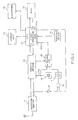
CPU 13 processes at high speed in accordance with the second clock signal the message signal into the processed message signal which is the processed message code. Namely, theCPU 13 is put into operation at a rapid processing speed by the second clock signal when the receivingsection 11 is put into operation. The second clock signal inevitably serves as a noise signal in the receivingsection 11. As a result, the receivingsection 11 is influenced by the noise signal so that its signal to noise ratio drops. Namely, it is difficult to maintain a satisfactory signal to noise ratio at the receivingsection 11. - Referring to Fig. 4, description will proceed to a radio paging receiver according to a first embodiment of this invention. The radio paging receiver comprises similar parts which are designated by like reference numerals and are operable with likewise named and denoted signals.
- As described above, the receiving
section 11 is intermittently put into receiving operation by the first operating signal which is supplied from thedecoder section 12. The receivingsection 11 intermittently demodulates the radio signal into the demodulated signal to supply the demodulated signal to thedecoder section 12 through a signal line depicted upwardly between the receivingsection 11 and thedecoder section 12. When thedecoder section 12 establishes synchronization of the demodulated signal, thedecoder section 12 supplies the receivingsection 11 with the second operating signal through a signal line which is depicted downwardly between the receivingsection 11 and thedecoder section 12 and through which the first operating signal is delivered to the receivingsection 11. The receivingsection 11 is intermittently put into receiving operation by the second operating signal. - In Fig. 4, the paging receiver further comprises a switching
circuit 20, aninverter 21, and an ANDgate 22. The switchingcircuit 20 is connected to the first and thesecond clock generators inverter 21 produces an inverted operating signal in response to the second operating signal. - The
first clock generator 16 supplies thedecoder section 12 with the first clock signal through a first supplyingline 16a. The switchingcircuit 20 is connected to theCPU 13 through a second supplyingline 20a. The switchingcircuit 20 selectively connects theCPU 13 to the first and thesecond clock generators decoder section 12. TheCPU 13 supplies the ANDgate 22 with a stand-by signal indicative of reception of the specific message signal. The ANDgate 22 supplies thesecond clock generator 17 with a driving signal when the second inverted operating signal and the stand-by signal is supplied. Thesecond clock generator 17 generates the second clock signal in response to the driving signal. - Referring to Fig. 5 together with Fig. 4, the
decoder section 12 is put into operation by the first clock signal which is supplied from thefirst clock generator 16 when thereceiver switch 15 is put into the on state. Thedecoder section 12 intermittently produces the first operating signal to supply the receivingsection 11 with the first operating signal. The receivingsection 11 is intermittently put into receiving operation by the first operating signal. - The
decoder section 12 has adata input terminal 23 and accepts the demodulated signal from the receivingsection 11 through thedata input terminal 23. Thedecoder section 12 comprises abit synchronization circuit 24, aframe synchronization circuit 25, a callsignal checking circuit 26, anerror correcting circuit 27, amessage buffer storage 28, and aninterface circuit 29. The demodulated signal is supplied to thebit synchronization circuit 24, theframe synchronization circuit 25, the callsignal checking circuit 26, and theerror correcting circuit 27. Thebit synchronization circuit 24 establishes bit synchronization of the demodulated signal with a bit synchronization clock signal which is produced in thedecoder 12 based on the first clock signal. Thebit synchronization circuit 24 supplies theframe synchronization circuit 25 with a bit synchronization signal. - The
frame synchronization circuit 25 comprises a preamblesignal detection circuit 25a, a frame synchronizationsignal detecting circuit 25b, a frame synchronization controlling circuit 25c, and aframe counter 25d. The frame synchronization controlling circuit 25c has a specific frame number of a frame in which the specific call signal is transmitted. The first operating signal is supplied from the frame synchronization controlling circuit 25c to the receivingsection 11. The preamblesignal detection circuit 25a detects the preamble signal of the demodulated signal to supply a preamble detection signal to the frame synchronization controlling circuit 25c. The frame synchronizationsignal detecting circuit 25b detects the frame synchronization signal to supply a frame detection signal to the frame synchronization controlling circuit 25c. The frame synchronization controlling circuit 25c establishes frame synchronization of the demodulated signal with the bit synchronization clock signal by using the bit synchronization signal, the preamble detection signal, and frame detection signal as known in the art. - When the frame synchronization is established, the frame synchronization controlling circuit 25c drives the
frame counter 25d. Theframe counter 25d starts to count the number of frames in each batch and supplies the frame synchronization controlling circuit 25c with a frame count signal which represents the number of each frame. When the frame number indicative of the frame count signal corresponds to the specific frame number, the frame synchronization controlling circuit 25c generates the second operating signal having a leading edge coincident with a leading edge of the specific frame. The second operating signal is supplied to the receivingsection 11 through an operatingsignal output terminal 30. - Turning to Fig. 6, the radio signal has a plurality of batches B(1), B(2), and so forth as shown along a first or top row labelled (a). The second frame F(2) of each batch B (suffixes omitted) is assigned to the group to which the radio paging receiver belongs. The second operating signal has a leading edge at the leading edge of each of the frames F(2) of the respective batches as shown along a second row labelled (b). The second operating signal has a trailing edge coincident with a trailing edge of an idle signal as will be described hereinafter. As a result, the receiving
section 11 is put into receiving operation during an operating time interval which is determined between the leading edge and the trailing edge of the second operating signal. - Each of the frames has a predetermined length. When the specific message signal indicates a specific message code which is longer than the predetermined length, the specific message signal is transmitted from the transmitting station to the radio paging receiver illustrated in Fig. 4 by using the second frame F(2) and the third frame F(3). The specific message signal is followed by an idle signal indicative of the end of the message signal as shown in the first row labelled (a). Another call signal assigned to another radio paging receiver may be transmitted by the second frame F(2) in the second batch B(2) as shown along the first row labelled (a). The other call signal is followed by an idle signal.
- Turning back to Fig. 5, the frame synchronization controlling circuit 25c drives the call
signal checking circuit 26 and theerror correcting circuit 27 when the frame synchronization is established. As a result, the callsignal checking circuit 26 checks the specific call signal of the second frame F(2) in the first batch B(1). Theerror correcting circuit 27 corrects the specific call signal of the second frame F(2) in the first batch B(1) to produce a corrected call signal. When the specific call signal corresponds to the call number assigned to the paging receiver, the callsignal checking circuit 26 produces a coincidence signal. The coincidence signal is supplied to theerror correcting circuit 27. Theerror correcting circuit 27 writes the corrected call signal as a specific call number to themessage buffer storage 28. Similarly, theerror correcting circuit 27 corrects the specific message signal succeeding the specific call signal to produce a corrected message signal and writes the corrected message signal as a specific message code in themessage buffer storage 28 in relation to the specific call number. The coincidence signal is supplied as an interrupt signal from an interrupt terminal 29a to theCPU 13 through theinterface circuit 29. - The second operating signal is supplied to a
delay circuit 25e to be given a predetermined delay (Δt) of, for example, 10 msec. Thedelay circuit 25e produces a delayed operating signal to supply the delayed operating signal to an OR gate 25f. The OR gate 25f produces the switching signal in response to the second operating signal and the delayed operating signal as shown along a third row labelled (c). The switching signal is supplied to the switchingcircuit 20 through a switchingsignal output terminal 31. - Again referring to Fig. 4 together with Figs. 5 and 6, the
CPU 13 is connected to thefirst clock generator 16 by the switchingcircuit 20 and is put into operation by the first clock signal. When the coincidence signal is supplied to theCPU 13, theCPU 13 is put into the interrupt mode as described above. The specific call number and the specific message code are supplied from themessage buffer storage 28 to theCPU 13 through theinterface circuit 29 and adata output terminal 29b. - The
CPU 13 comprises asignal producing part 13a. When thesignal producing part 13a receives the specific message code, thesignal producing part 13a produces the stand-by signal indicative of reception of the specific message code to supply the ANDgate 22 with the stand-by signal as shown in a fourth row labelled (d). Otherwise, the inverted operating signal is supplied to the ANDgate 21. The ANDgate 21 produces the driving signal. The driving signal has a leading edge coincident with the leading edge of the inverted operating signal and a trailing edge coincident with the trailing edge of the stand-by signal as shown in a fifth row labelled (e). - The
CPU 13 carries out an interrupt processing similar to the interrupt processing shown in Fig. 3 when supplied with the coincidence signal. When theCPU 13 detects the idle signal, theCPU 13 produces the control signal. The control signal is supplied from theCPU 13 to the frame synchronization controlling circuit 25c through a controlsignal input terminal 29c and theinterface circuit 29. The frame synchronization controlling circuit 25c stops supply of the second operating signal in response to the control signal. As a result, the receivingsection 11 stops a receiving operation. The OR gate 25f stops delivery of the switching signal when the predetermined delay (Δt) lapses from stop of receiving operation. - The
second clock generator 17 is driven in response to the leading edge of the driving signal and generates the second clock signal. The switchingcircuit 20 connects thesecond clock generator 17 with theCPU 13 in response to the trailing edge of the switching signal after the predetermined delay (Δt). As a result, theCPU 13 is put in the main processing mode from the interrupt mode. - The
CPU 13 is put into operation at a rapid speed by the second clock signal in the main processing mode. TheCPU 13 carries out a main processing similar to the main processing shown in Fig. 3. When theCPU 13 ends the main processing, thesignal producing part 13a stops supply of the stand-by signal. Thesecond clock generator 17 stops generation of the second clock signal. - As described above, the
CPU 13 is put into operation by the first clock signal in the interrupt mode and is put into operation by the second clock signal in the main processing mode. - Continuously referring to Figs. 4 to 6, the
decoder section 12 supplies the receivingsection 11 with the second operating signal of which a leading edge is coincident with the leading edge of the second frame F(2) in the second batch B(2) as shown in the first row labelled (a). The receivingsection 11 is put into operation. Thedecoder section 12 supplies the switchingcircuit 20 with the switching signal having a leading edge coincident with the leading edge of the second operating signal. The switchingcircuit 20 connects theCPU 13 with thefirst clock generator 16 in response to the leading edge of the switching signal. TheCPU 13 is put into operation by the first clock signal. - In case where another call signal which is assigned to another radio paging receiver is transmitted in the second frame F(2) of the second batch B(2), the call
signal checking circuit 26 judges that the other call signal does not correspond to the specific call signal. The callsignal checking circuit 26 produces a discrepancy signal to supply the frame synchronization controlling circuit 25c with the discrepancy signal. - When supplied with the discrepancy signal, the frame synchronization controlling circuit 25c continues delivery of the second operating signal during the interval of the second frame F(2) as shown in the second row labelled (b). The frame synchronization controlling circuit 25c stops supply of the second operating signal as shown in the second row labelled (b) after the interval of the second frame F(2) lapses.
- When the predetermined delay (Δt) lapses after stop of the second operating signal, the delayed operating signal is stopped as described above. As a result, supply of the switching signal is stopped. The switching
circuit 20 connects theCPU 13 with thesecond generator 17 in response to the trailing edge of the switching signal. In this event, thesignal producing part 13a does not produce the stand-by signal because thesignal producing part 13a does not receive the specific call signal. Therefore, thesecond clock generator 17 does not generate the second clock signal so that the second clock signal is not supplied to theCPU 13. - Referring now to Fig. 7, description will be directed to a radio paging receiver according to a second embodiment of this invention. In the second embodiment, the
second clock generator 17 andclock switching circuit 20 is controlled by the CPU software. The radio paging receiver comprises similar parts which are designated by like reference numerals and are operable with likewise named and denoted signals. - As in the conventional radio paging receiver and in the radio paging receiver illustrated with reference to Fig. 4, the
second decoder section 12 is put into operation by the first clock signal. Thedecoder section 12 intermittently supplies the second operating signal to the receivingsection 11 and theCPU 13. - The receiving
section 11 is put into receiving operation by the second operating signal and supplies thedecoder section 12 with the demodulated signal. Thedecoder section 12 is responsive to the demodulated signal and distinguishes the specific call signal from the plurality of call signals to supply theCPU 13 with the coincident signal. - Referring to Figs. 8 and 9 together with Fig. 7, the
CPU 13 is connected to thefirst clock generator 16 through the switchingcircuit 20. TheCPU 13 is put into operation by the first clock signal. Thedecoder section 12 supplies theCPU 13 with the second operating signal as shown in Fig. 9 along a first or top row labelled (a) after the establishment of synchronization. TheCPU 13 is put into the interrupt mode when supplied with the coincident signal. - After put into the interrupt mode, the
CPU 13 detects whether the specific message signal M is supplied from thedecoder section 12 or not as shown at a first step SS1 by a mere notation of M. When theCPU 13 does not detect supply of the specific message signal, the first step SS1 is again executed. When theCPU 13 detects supply of the specific message signal, the first step SS1 proceeds to a second step SS2 at which operation is carried out to detect whether the second operating signal OP is supplied from thedecoder section 12 or not as indicated merely by OP. When theCPU 13 detects supply of the second operating signal OP, the second step SS2 is repeatedly executed. - When the
CPU 13 does not detect the second operating signal, namely, the receivingsection 11 is not put into receiving operation, the second step SS2 is followed by a third step SS3 at which operation is carried out to produce the stand-by signal ST as a driving signal as indicated merely by ST. The stand-by signal has a leading edge coincident with the trailing edge of the second operating signal as shown in a second row labelled (b). Thesecond clock generator 17 produces the second clock signal in response to a leading edge of the stand-by signal. - The third step SS3 proceeds to a fourth step SS4 at which operation is carried to detect whether or not the predetermined delay Δ t) lapses as indicated merely by Δt after stop of the second operating signal. When the predetermined delay (Δt) does not lapse, the fourth step SS4 is again executed. When the predetermined delay (Δt) lapses, the fourth step SS4 proceeds to a fifth step SS5 at which operation is carried out to produce the switching signal SW as shown in a third row labelled (c). The switching
circuit 20 connects thesecond clock generator 17 with theCPU 13 in response to the leading edge of the switching signal. As a result, the second clock signal is supplied to theCPU 13 as shown in a fourth row labelled (d). When theCPU 13 supplies the switchingcircuit 20 with the switching signal, theCPU 13 is put into the main processing mode. TheCPU 13 processes the specific message code into the processed message code at a rapid processing speed. - The fifth step SS5 is followed by a sixth step SS6 at which operation is carried out to judge whether the main processing ends or not as indicated merely by MP. When the main processing does not end, the sixth step is repeatedly executed. When the main processing ends, the
CPU 13 stops supply of the switching signal SW and the stand-by signal ST as shown in the second and third rows labelled (b) and (c), respectively, in a seventh step SS7. Thesecond clock generator 17 stops generation of the second clock signal in response to the trailing edge of the stand-by signal. The switchingcircuit 20 connects theCPU 13 with thefirst clock generator 16 in response to the trailing edge of the switching signal. The first clock signal is supplied to theCPU 13 as shown in the fourth row labelled (d). Operation returns back to the first step SS1.
Claims (3)
first clock generating means for generating a first clock signal having a first frequency;
second clock generating means for generating a second clock signal having a second frequency higher than said first frequency;
first supplying means for supplying said distinguishing means with said first clock signal to operate said distinguishing means; and
second supplying means for supplying said processing means with either said first clock signal or said second clock signal and for suppressing said clock signal at least when said receiving means operates.
said apparatus further comprises:
delaying means for delaying said operating signal with a predetermined time duration to produce a delayed operating signal;
switching signal producing means for producing a switching signal in response to said operating signal and said delayed operating signal; and
stand-by signal producing means connected to said distinguishing means for producing a stand-by signal indicative of reception of said specific additional signal when said distinguishing means distinguishes said specific one of said call signals;
said second supplying means comprising:
driving means responsive to said operating signal and said stand-by signal for driving said second clock generating means; and
switching means responsive to said switching signal for connecting said second clock generating means to said processing means.
said apparatus further comprises:
driving signal producing means for producing a driving signal for use in driving said second clock generating means when said operating signal producing means stops producing said operating signal; and
switching signal producing means responsive to said operating signal for producing a switching signal after a predetermined time duration;
said second supplying means comprises:
switching means responsive to said switching signal for connecting said second clock generating means to said processing means.
Applications Claiming Priority (2)
| Application Number | Priority Date | Filing Date | Title |
|---|---|---|---|
| JP63175213A JPH0744477B2 (en) | 1988-07-15 | 1988-07-15 | Small digital radio receiver |
| JP175213/88 | 1988-07-15 |
Publications (3)
| Publication Number | Publication Date |
|---|---|
| EP0351230A2 true EP0351230A2 (en) | 1990-01-17 |
| EP0351230A3 EP0351230A3 (en) | 1991-10-23 |
| EP0351230B1 EP0351230B1 (en) | 1994-10-26 |
Family
ID=15992274
Family Applications (1)
| Application Number | Title | Priority Date | Filing Date |
|---|---|---|---|
| EP89307152A Expired - Lifetime EP0351230B1 (en) | 1988-07-15 | 1989-07-14 | Radio communication apparatus having an improved signal to noise ratio |
Country Status (8)
| Country | Link |
|---|---|
| US (1) | US5142699A (en) |
| EP (1) | EP0351230B1 (en) |
| JP (1) | JPH0744477B2 (en) |
| KR (1) | KR920009400B1 (en) |
| AU (1) | AU631556B2 (en) |
| CA (1) | CA1313227C (en) |
| DE (1) | DE68919002T2 (en) |
| HK (1) | HK84797A (en) |
Cited By (14)
| Publication number | Priority date | Publication date | Assignee | Title |
|---|---|---|---|---|
| EP0463621A1 (en) * | 1990-06-28 | 1992-01-02 | Firma Erika Köchler | Receiver for digital radio signals |
| EP0509649A2 (en) * | 1991-03-30 | 1992-10-21 | Nec Corporation | Selective calling receiver |
| EP0511511A2 (en) * | 1991-04-30 | 1992-11-04 | Motorola Israel Limited | Microprocessor controlled electronic equipment |
| EP0553862A2 (en) * | 1992-01-31 | 1993-08-04 | Canon Kabushiki Kaisha | Portable electronic device having a radio transmit-receive unit and a computer unit |
| FR2699027A1 (en) * | 1992-12-04 | 1994-06-10 | Info Telecom | Method for processing information within a receiver, in particular paging, and corresponding receiver. |
| EP0661892A2 (en) * | 1993-12-28 | 1995-07-05 | Nec Corporation | Portable information equipment system and control method thereof |
| EP0667062A1 (en) * | 1993-07-01 | 1995-08-16 | Motorola, Inc. | Expanded microcomputer system for controlling radio frequency interference |
| GB2297883A (en) * | 1995-02-07 | 1996-08-14 | Nokia Mobile Phones Ltd | Battery saving method for a mobile telephone |
| GB2311192A (en) * | 1996-03-13 | 1997-09-17 | Nec Corp | Data Transmitter/Receiver |
| EP0831595A2 (en) * | 1996-09-18 | 1998-03-25 | Nec Corporation | Digital modulated signal receiver |
| US5737323A (en) * | 1995-02-07 | 1998-04-07 | Nokia Mobile Phones Limited | Radio telephone |
| US5740129A (en) * | 1995-02-07 | 1998-04-14 | Nokia Mobile Phones Limited | Real time clock |
| WO2001039406A2 (en) * | 1999-11-25 | 2001-05-31 | Siemens Aktiengesellschaft | Method for effecting the interference-reduced operation of a radio transceiver and a radio transceiver |
| EP1168634A1 (en) * | 2000-06-28 | 2002-01-02 | STMicroelectronics N.V. | Method for reducing the electricity consumption of a mobile cellular telephone |
Families Citing this family (35)
| Publication number | Priority date | Publication date | Assignee | Title |
|---|---|---|---|---|
| JP2864743B2 (en) * | 1990-12-20 | 1999-03-08 | 日本電気株式会社 | Radio selective calling system and receiver used for it |
| AU642097B2 (en) * | 1991-11-01 | 1993-10-07 | Keith Robert Hockley | Remote control pager system |
| JPH0678008A (en) * | 1992-08-24 | 1994-03-18 | Uniden Corp | Code receiver |
| FI95980C (en) * | 1992-09-04 | 1996-04-10 | Nokia Mobile Phones Ltd | Method and switchgear for accurate measurement of time with an inaccurate clock |
| CA2108244C (en) * | 1992-10-12 | 1999-12-28 | Motoki Ide | Selectively called radio receiver in which bit rate detection is controlled with a predetermined range |
| US5765113A (en) * | 1994-12-29 | 1998-06-09 | Russo; David William | Method and apparatus for avoiding desensitization of a radio frequency receiver |
| US5630224A (en) * | 1994-12-29 | 1997-05-13 | Motorola, Inc. | Method and apparatus for avoiding desensitization of a radio frequency receiver |
| US5799023A (en) * | 1995-07-19 | 1998-08-25 | Matsushita Electric Industrial Co., Ltd. | Message receiver |
| US5845204A (en) * | 1995-08-11 | 1998-12-01 | Rockwell International Corporation | Method and apparatus for controlling the wakeup logic of a radio receiver in sleep mode |
| JP3719287B2 (en) * | 1996-04-16 | 2005-11-24 | ソニー株式会社 | Receiving apparatus, receiving method, and communication system |
| US6009319A (en) * | 1996-09-06 | 1999-12-28 | Telefonaktiebolaget Lm Ericsson | Method and apparatus for reducing power consumption in a mobile radio communication device |
| CN1126378C (en) * | 1997-01-17 | 2003-10-29 | 松下电器产业株式会社 | Message receiver |
| JP3570846B2 (en) * | 1997-03-27 | 2004-09-29 | Necアクセステクニカ株式会社 | Wireless personal digital assistant |
| US5950120A (en) * | 1997-06-17 | 1999-09-07 | Lsi Logic Corporation | Apparatus and method for shutdown of wireless communications mobile station with multiple clocks |
| SG67419A1 (en) * | 1997-09-19 | 1999-09-21 | For Wireless Communications Na | A contactless identification and communication system and method of operating the same |
| US6088602A (en) * | 1998-03-27 | 2000-07-11 | Lsi Logic Corporation | High resolution frequency calibrator for sleep mode clock in wireless communications mobile station |
| US7324496B1 (en) | 2002-05-01 | 2008-01-29 | Nxp B.V. | Highly integrated radio-frequency apparatus and associated methods |
| CA2393651A1 (en) * | 2002-07-29 | 2004-01-29 | Ralph Dickson Mason | Low power oscillator and power down method |
| US8478921B2 (en) * | 2004-03-31 | 2013-07-02 | Silicon Laboratories, Inc. | Communication apparatus implementing time domain isolation with restricted bus access |
| US8884791B2 (en) * | 2004-06-29 | 2014-11-11 | St-Ericsson Sa | Keypad scanning with radio event isolation |
| US7248848B2 (en) * | 2004-06-30 | 2007-07-24 | Matthews Phillip M | Communication apparatus including dual timer units |
| US7433393B2 (en) | 2004-07-23 | 2008-10-07 | Nxp B.V. | Apparatus for controlling a digital signal processor for radio isolation and associated methods |
| US8472990B2 (en) * | 2004-07-23 | 2013-06-25 | St Ericsson Sa | Apparatus using interrupts for controlling a processor for radio isolation and associated method |
| US7761056B2 (en) * | 2004-07-23 | 2010-07-20 | St-Ericsson Sa | Method of controlling a processor for radio isolation using a timer |
| US20050008095A1 (en) * | 2004-07-23 | 2005-01-13 | Rush Frederick A. | Apparatus using interrupts for controlling a processor for radio isolation and associated methods |
| US7567637B2 (en) | 2004-09-30 | 2009-07-28 | St-Ericsson Sa | Wireless communication system and method with frequency burst acquisition feature using autocorrelation and narrowband interference detection |
| US7593482B2 (en) * | 2004-09-30 | 2009-09-22 | St-Ericsson Sa | Wireless communication system with hardware-based frequency burst detection |
| US7778674B2 (en) * | 2004-12-29 | 2010-08-17 | St-Ericsson Sa | Communication apparatus having a SIM interface compatible with radio isolation |
| US8019382B2 (en) * | 2004-12-29 | 2011-09-13 | St-Ericsson Sa | Communication apparatus having a standard serial communication interface compatible with radio isolation |
| US7805170B2 (en) * | 2005-03-30 | 2010-09-28 | St-Ericsson Sa | System and method for efficient power supply regulation compatible with radio frequency operation |
| US7209061B2 (en) | 2005-03-30 | 2007-04-24 | Silicon Laboratories, Inc. | Method and system for sampling a signal |
| US7283503B1 (en) | 2005-06-24 | 2007-10-16 | Silicon Laboratories, Inc. | Communication apparatus including a buffer circuit having first and second portions for alternately storing results |
| US7801207B2 (en) * | 2005-06-24 | 2010-09-21 | St-Ericsson Sa | Signal processing task scheduling in a communication apparatus |
| US7414560B2 (en) * | 2005-06-29 | 2008-08-19 | Shaojie Chen | Wireless communication system including an audio underflow protection mechanism operative with time domain isolation |
| FR2895200B1 (en) * | 2005-12-20 | 2008-02-22 | Silicon Lab Inc | METHOD FOR ACQUIRING A FREQUENCY CORRECTION BURST BY A RADIO COMMUNICATION DEVICE, AND CORRESPONDING RADIO COMMUNICATION DEVICE |
Citations (4)
| Publication number | Priority date | Publication date | Assignee | Title |
|---|---|---|---|---|
| EP0032598A1 (en) * | 1980-01-17 | 1981-07-29 | Ascom Autophon Ag | Portable paging receiver with a shift register and a direct current converter |
| US4384361A (en) * | 1979-09-29 | 1983-05-17 | Nippon Electric Co., Ltd. | Selective calling receiver |
| JPS59200537A (en) * | 1983-04-27 | 1984-11-13 | Nippon Telegr & Teleph Corp <Ntt> | Mobile communication equipment |
| GB2149164A (en) * | 1983-09-30 | 1985-06-05 | Nec Corp | Pager receiver |
Family Cites Families (11)
| Publication number | Priority date | Publication date | Assignee | Title |
|---|---|---|---|---|
| AU5052069A (en) * | 1969-02-14 | 1970-08-20 | Communications Associates Limited | Improvements intwo-tone frequency modulated communication systems |
| JPS6035389A (en) * | 1983-08-05 | 1985-02-23 | Pioneer Electronic Corp | Display device for amount of tape |
| JPS6098583A (en) * | 1983-11-01 | 1985-06-01 | Matsushita Electric Ind Co Ltd | Acoustic device |
| JPS6192045A (en) * | 1984-10-12 | 1986-05-10 | Nec Corp | Radio selective call receiver with message |
| JPS61258529A (en) * | 1985-05-13 | 1986-11-15 | Nec Corp | Frequency synthesizer |
| CA1282464C (en) * | 1985-10-23 | 1991-04-02 | Masanori Ienaka | Phase-locked oscillator |
| JPS6313432A (en) * | 1986-07-03 | 1988-01-20 | Kokusai Electric Co Ltd | Battery saving method for receiver in selecting calling signal system |
| JPS63141420A (en) * | 1986-12-03 | 1988-06-13 | Fuji Electric Co Ltd | Call signal receiver |
| US4860005A (en) * | 1988-01-07 | 1989-08-22 | Motorola, Inc. | Communication receiver with automatic turn on/off |
| JPH01190054A (en) * | 1988-01-25 | 1989-07-31 | Man Design Kk | Receiver |
| US4928086A (en) * | 1989-01-30 | 1990-05-22 | Motorola, Inc. | Pager receiver having a common timer circuit for both sequential lock-out and out-of-range |
-
1988
- 1988-07-15 JP JP63175213A patent/JPH0744477B2/en not_active Expired - Fee Related
-
1989
- 1989-07-14 CA CA000605663A patent/CA1313227C/en not_active Expired - Fee Related
- 1989-07-14 DE DE68919002T patent/DE68919002T2/en not_active Expired - Fee Related
- 1989-07-14 EP EP89307152A patent/EP0351230B1/en not_active Expired - Lifetime
- 1989-07-15 KR KR8910150A patent/KR920009400B1/en not_active IP Right Cessation
- 1989-07-17 AU AU38168/89A patent/AU631556B2/en not_active Ceased
-
1991
- 1991-09-05 US US07/759,040 patent/US5142699A/en not_active Expired - Lifetime
-
1997
- 1997-06-19 HK HK84797A patent/HK84797A/en not_active IP Right Cessation
Patent Citations (4)
| Publication number | Priority date | Publication date | Assignee | Title |
|---|---|---|---|---|
| US4384361A (en) * | 1979-09-29 | 1983-05-17 | Nippon Electric Co., Ltd. | Selective calling receiver |
| EP0032598A1 (en) * | 1980-01-17 | 1981-07-29 | Ascom Autophon Ag | Portable paging receiver with a shift register and a direct current converter |
| JPS59200537A (en) * | 1983-04-27 | 1984-11-13 | Nippon Telegr & Teleph Corp <Ntt> | Mobile communication equipment |
| GB2149164A (en) * | 1983-09-30 | 1985-06-05 | Nec Corp | Pager receiver |
Non-Patent Citations (1)
| Title |
|---|
| PATENT ABSTRACTS OF JAPAN vol. 9, no. 61 (E-303)(1784) March 19, 1985 & JP-A-59 200 537 (NIPPON DENSHIN DENWA KOSHA ) November 13, 1984 * |
Cited By (29)
| Publication number | Priority date | Publication date | Assignee | Title |
|---|---|---|---|---|
| EP0463621A1 (en) * | 1990-06-28 | 1992-01-02 | Firma Erika Köchler | Receiver for digital radio signals |
| CH680343A5 (en) * | 1990-06-28 | 1992-08-14 | Erika Koechler | |
| EP0509649A2 (en) * | 1991-03-30 | 1992-10-21 | Nec Corporation | Selective calling receiver |
| EP0509649A3 (en) * | 1991-03-30 | 1993-06-09 | Nec Corporation | Selective calling receiver |
| EP0511511A2 (en) * | 1991-04-30 | 1992-11-04 | Motorola Israel Limited | Microprocessor controlled electronic equipment |
| EP0511511A3 (en) * | 1991-04-30 | 1993-05-12 | Motorola Israel Limited | Microprocessor controlled radio transceiver |
| EP0553862A2 (en) * | 1992-01-31 | 1993-08-04 | Canon Kabushiki Kaisha | Portable electronic device having a radio transmit-receive unit and a computer unit |
| EP0553862A3 (en) * | 1992-01-31 | 1994-11-17 | Canon Kk | Portable electronic device having a radio transmit-receive unit and a computer unit |
| US5604928A (en) * | 1992-01-31 | 1997-02-18 | Canon Kabushiki Kaisha | Portable electronic device with radio communication and controlled computer status |
| FR2699027A1 (en) * | 1992-12-04 | 1994-06-10 | Info Telecom | Method for processing information within a receiver, in particular paging, and corresponding receiver. |
| WO1994014290A1 (en) * | 1992-12-04 | 1994-06-23 | Info Telecom | Method for processing information within a receiver, particularly a paging receiver, and receiver therefor |
| EP0667062A4 (en) * | 1993-07-01 | 1999-06-23 | Motorola Inc | Expanded microcomputer system for controlling radio frequency interference. |
| EP0667062A1 (en) * | 1993-07-01 | 1995-08-16 | Motorola, Inc. | Expanded microcomputer system for controlling radio frequency interference |
| EP0661892A3 (en) * | 1993-12-28 | 1997-02-26 | Nec Corp | Portable information equipment system and control method thereof. |
| EP0661892A2 (en) * | 1993-12-28 | 1995-07-05 | Nec Corporation | Portable information equipment system and control method thereof |
| US5737323A (en) * | 1995-02-07 | 1998-04-07 | Nokia Mobile Phones Limited | Radio telephone |
| GB2297883B (en) * | 1995-02-07 | 1999-08-11 | Nokia Mobile Phones Ltd | Radio telephone |
| GB2297883A (en) * | 1995-02-07 | 1996-08-14 | Nokia Mobile Phones Ltd | Battery saving method for a mobile telephone |
| US5740129A (en) * | 1995-02-07 | 1998-04-14 | Nokia Mobile Phones Limited | Real time clock |
| US5758278A (en) * | 1995-02-07 | 1998-05-26 | Nokia Mobile Phones Limited | Method and apparatus for periodically re-activating a mobile telephone system clock prior to receiving polling signals |
| GB2311192A (en) * | 1996-03-13 | 1997-09-17 | Nec Corp | Data Transmitter/Receiver |
| US5920592A (en) * | 1996-03-13 | 1999-07-06 | Nec Corporation | Data transmitter-receiver |
| GB2311192B (en) * | 1996-03-13 | 2000-04-12 | Nec Corp | Data-transmitter-receiver and method of operation |
| EP0831595A2 (en) * | 1996-09-18 | 1998-03-25 | Nec Corporation | Digital modulated signal receiver |
| EP0831595A3 (en) * | 1996-09-18 | 2003-03-19 | Nec Corporation | Digital modulated signal receiver |
| WO2001039406A2 (en) * | 1999-11-25 | 2001-05-31 | Siemens Aktiengesellschaft | Method for effecting the interference-reduced operation of a radio transceiver and a radio transceiver |
| WO2001039406A3 (en) * | 1999-11-25 | 2001-12-27 | Siemens Ag | Method for effecting the interference-reduced operation of a radio transceiver and a radio transceiver |
| EP1168634A1 (en) * | 2000-06-28 | 2002-01-02 | STMicroelectronics N.V. | Method for reducing the electricity consumption of a mobile cellular telephone |
| US6876874B2 (en) | 2000-06-28 | 2005-04-05 | Stmicroelectronics N.V. | Process for reducing the electrical consumption of a transmitter/receiver of digital information, in particular a cellular mobile telephone, and corresponding transmitter/receiver |
Also Published As
| Publication number | Publication date |
|---|---|
| HK84797A (en) | 1997-06-27 |
| JPH0226131A (en) | 1990-01-29 |
| AU3816889A (en) | 1990-01-18 |
| DE68919002D1 (en) | 1994-12-01 |
| EP0351230A3 (en) | 1991-10-23 |
| KR920009400B1 (en) | 1992-10-16 |
| US5142699A (en) | 1992-08-25 |
| AU631556B2 (en) | 1992-12-03 |
| JPH0744477B2 (en) | 1995-05-15 |
| CA1313227C (en) | 1993-01-26 |
| KR900002582A (en) | 1990-02-28 |
| DE68919002T2 (en) | 1995-06-01 |
| EP0351230B1 (en) | 1994-10-26 |
Similar Documents
| Publication | Publication Date | Title |
|---|---|---|
| US5142699A (en) | Radio receiver with clock signal controlled to improve the signal to noise ratio | |
| EP0154288B1 (en) | Method of transmitting terminating call signals within a restricted duration and a base station and a portable unit for use in the same | |
| US6078631A (en) | Wireless communication system compulsively turning remote terminals into inactive state | |
| EP0091695B1 (en) | Battery saver circuit for use with paging receiver | |
| US5230084A (en) | Selective call receiver having extended battery saving capability | |
| JPH0431448B2 (en) | ||
| JPH0412052B2 (en) | ||
| EP0124788A1 (en) | Radio paging system and receiver therefor | |
| EP0717510A2 (en) | Circuit and method for controlling a timing of intermittent reception in radio equipment | |
| EP0554941A1 (en) | Battery power conservation in a selective call system | |
| RU2178238C2 (en) | Discriminating-call system and its secondary station | |
| EP0443516B1 (en) | Transmission and reception of pager signals without useless sampling operation | |
| US6216385B1 (en) | Radio calling receiver with means to control reception based on service area, time zone, and/or electric field strength | |
| US6215980B1 (en) | Apparatus and method for saving battery power of a paging receiver | |
| EP0509649B1 (en) | Selective calling receiver | |
| EP0649209B1 (en) | Power supply control for a receiver | |
| JP2965566B2 (en) | Selective call receiver and receiver | |
| JP2581719B2 (en) | Selective call communication method | |
| JP2982515B2 (en) | Radio selective call receiver | |
| JP2928806B2 (en) | Selective calling method | |
| JP2690343B2 (en) | Wireless paging method | |
| JP2822523B2 (en) | Data transmission method, data receiver, and data transmission system | |
| JPH0583187A (en) | Battery saving for pager | |
| JPH0537446A (en) | Selection call communication system | |
| JPH0226137A (en) | Radio calling receiver |
Legal Events
| Date | Code | Title | Description |
|---|---|---|---|
| PUAI | Public reference made under article 153(3) epc to a published international application that has entered the european phase |
Free format text: ORIGINAL CODE: 0009012 |
|
| 17P | Request for examination filed |
Effective date: 19890811 |
|
| AK | Designated contracting states |
Kind code of ref document: A2 Designated state(s): DE GB NL |
|
| PUAL | Search report despatched |
Free format text: ORIGINAL CODE: 0009013 |
|
| AK | Designated contracting states |
Kind code of ref document: A3 Designated state(s): DE GB NL |
|
| 17Q | First examination report despatched |
Effective date: 19930907 |
|
| GRAA | (expected) grant |
Free format text: ORIGINAL CODE: 0009210 |
|
| AK | Designated contracting states |
Kind code of ref document: B1 Designated state(s): DE GB NL |
|
| REF | Corresponds to: |
Ref document number: 68919002 Country of ref document: DE Date of ref document: 19941201 |
|
| PLBE | No opposition filed within time limit |
Free format text: ORIGINAL CODE: 0009261 |
|
| STAA | Information on the status of an ep patent application or granted ep patent |
Free format text: STATUS: NO OPPOSITION FILED WITHIN TIME LIMIT |
|
| 26N | No opposition filed | ||
| REG | Reference to a national code |
Ref country code: GB Ref legal event code: IF02 |
|
| PGFP | Annual fee paid to national office [announced via postgrant information from national office to epo] |
Ref country code: NL Payment date: 20020730 Year of fee payment: 14 |
|
| PG25 | Lapsed in a contracting state [announced via postgrant information from national office to epo] |
Ref country code: NL Free format text: LAPSE BECAUSE OF NON-PAYMENT OF DUE FEES Effective date: 20040201 |
|
| NLV4 | Nl: lapsed or anulled due to non-payment of the annual fee |
Effective date: 20040201 |
|
| PGFP | Annual fee paid to national office [announced via postgrant information from national office to epo] |
Ref country code: DE Payment date: 20070712 Year of fee payment: 19 |
|
| PGFP | Annual fee paid to national office [announced via postgrant information from national office to epo] |
Ref country code: GB Payment date: 20070711 Year of fee payment: 19 |
|
| GBPC | Gb: european patent ceased through non-payment of renewal fee |
Effective date: 20080714 |
|
| PG25 | Lapsed in a contracting state [announced via postgrant information from national office to epo] |
Ref country code: DE Free format text: LAPSE BECAUSE OF NON-PAYMENT OF DUE FEES Effective date: 20090203 |
|
| PG25 | Lapsed in a contracting state [announced via postgrant information from national office to epo] |
Ref country code: GB Free format text: LAPSE BECAUSE OF NON-PAYMENT OF DUE FEES Effective date: 20080714 |