EP0352633A2 - A pipeline having an integral cache for computer processors - Google Patents
A pipeline having an integral cache for computer processors Download PDFInfo
- Publication number
- EP0352633A2 EP0352633A2 EP89113324A EP89113324A EP0352633A2 EP 0352633 A2 EP0352633 A2 EP 0352633A2 EP 89113324 A EP89113324 A EP 89113324A EP 89113324 A EP89113324 A EP 89113324A EP 0352633 A2 EP0352633 A2 EP 0352633A2
- Authority
- EP
- European Patent Office
- Prior art keywords
- data
- cache
- pipeline
- store
- entries
- Prior art date
- Legal status (The legal status is an assumption and is not a legal conclusion. Google has not performed a legal analysis and makes no representation as to the accuracy of the status listed.)
- Granted
Links
Images


Classifications
-
- G—PHYSICS
- G06—COMPUTING; CALCULATING OR COUNTING
- G06F—ELECTRIC DIGITAL DATA PROCESSING
- G06F9/00—Arrangements for program control, e.g. control units
- G06F9/06—Arrangements for program control, e.g. control units using stored programs, i.e. using an internal store of processing equipment to receive or retain programs
- G06F9/30—Arrangements for executing machine instructions, e.g. instruction decode
- G06F9/38—Concurrent instruction execution, e.g. pipeline, look ahead
-
- G—PHYSICS
- G06—COMPUTING; CALCULATING OR COUNTING
- G06F—ELECTRIC DIGITAL DATA PROCESSING
- G06F15/00—Digital computers in general; Data processing equipment in general
- G06F15/76—Architectures of general purpose stored program computers
- G06F15/80—Architectures of general purpose stored program computers comprising an array of processing units with common control, e.g. single instruction multiple data processors
- G06F15/8053—Vector processors
- G06F15/8061—Details on data memory access
- G06F15/8069—Details on data memory access using a cache
-
- G—PHYSICS
- G06—COMPUTING; CALCULATING OR COUNTING
- G06F—ELECTRIC DIGITAL DATA PROCESSING
- G06F12/00—Accessing, addressing or allocating within memory systems or architectures
- G06F12/02—Addressing or allocation; Relocation
- G06F12/08—Addressing or allocation; Relocation in hierarchically structured memory systems, e.g. virtual memory systems
- G06F12/0802—Addressing of a memory level in which the access to the desired data or data block requires associative addressing means, e.g. caches
- G06F12/0844—Multiple simultaneous or quasi-simultaneous cache accessing
- G06F12/0855—Overlapped cache accessing, e.g. pipeline
- G06F12/0859—Overlapped cache accessing, e.g. pipeline with reload from main memory
-
- G—PHYSICS
- G06—COMPUTING; CALCULATING OR COUNTING
- G06F—ELECTRIC DIGITAL DATA PROCESSING
- G06F15/00—Digital computers in general; Data processing equipment in general
- G06F15/76—Architectures of general purpose stored program computers
- G06F15/80—Architectures of general purpose stored program computers comprising an array of processing units with common control, e.g. single instruction multiple data processors
- G06F15/8053—Vector processors
- G06F15/8076—Details on data register access
- G06F15/8084—Special arrangements thereof, e.g. mask or switch
-
- G—PHYSICS
- G06—COMPUTING; CALCULATING OR COUNTING
- G06F—ELECTRIC DIGITAL DATA PROCESSING
- G06F9/00—Arrangements for program control, e.g. control units
- G06F9/06—Arrangements for program control, e.g. control units using stored programs, i.e. using an internal store of processing equipment to receive or retain programs
- G06F9/30—Arrangements for executing machine instructions, e.g. instruction decode
- G06F9/38—Concurrent instruction execution, e.g. pipeline, look ahead
- G06F9/3824—Operand accessing
- G06F9/383—Operand prefetching
Definitions
- Scalar processors in which instructions are pipelined would also benefit from the use of a cache which is integral to the pipeline. Again, the problem of multiple cache misses can cause the pipeline to be dominated by the servicing of those misses.
- the pipe entry and a hit or miss signal is then sent to the cache data storage stage 18.
- the data cache 38 has the physical address of a cache location and will either read data from or write data to that location, as long as there is a hit signal at the cache data storage stage 18.
- the data cache 38 is connected to a cache data bus 40 via a latch 19.
- Vector register files 42 which use the data from the cache 38 are also coupled to the cache data bus 40.
- the load/store pipeline 8 operates in one of three modes, as determined by a load/store controller 52. These modes are the load mode, the store mode and the cache fill mode. In the load mode, data is loaded from the data cache 38 to a vector register 42. During a store mode, data is conditionally stored into the data cache 38 from a vector register 42 depending whether the data misses or hits. The cache fill mode will be described later.
- the load/store controller sends out signals to the pipeline stages which inform the stages what mode the pipeline is to be in.
- the servicing of a read miss during a load operation includes obtaining the requested data from another processor or main memory via the external bus 50. The requested data is filled into the data cache 38 at the specified physical address and then driven onto the cache data bus 40 to the vector register file 42.
- the FIFO's 54, 56 are of a size such that they can take one complete vector store operation. This allows the pipeline 8 to be used for a simultaneous load operation.
- One embodiment has the load operation wait for the store operation to complete if a read miss occurs during the load operation. Should there be a translation buffer miss during the store operation, the store operation will be stopped and the read miss serviced over the external bus 50. In other words, the translation buffer miss operation has priority over the store operation in the use of the external bus 50.
- a single pipe entry represents four aligned quadword elements (a hexaword).
- the pipe entry is decomposed in the cache tag look up stage 14 into its component quadwords, these quadword addresses being fetched one at a time from the data cache 38. Since only one quadword per cycle can be delivered from the data cache 38, the address generator 10 is stalled during the decomposition until the last quadword of the hexaword is reached. If there is a read miss, then the entire hexaword will be retrieved and eventually filled to the read miss buffers 26a-d and the data cache 38.
- Another embodiment loads single quadword elements on hits, but after a read miss, will retrieve a hexaword to which the quadword that missed belonged.
- the hexaword is decomposed, but only the quadword that missed is loaded into the vector register file 42, while the entire hexaword is filled into the cache 38.
- Figures 2-4 show some of the components of Figure 1, reconfigured for purposes of explanation in the drawing to show the timing of the various operations.
- stage 1S the virtual address is generated and the RFA is driven out of the address generator stage 10.
- stage 2S the virtual address is translated into a physical address, and the RFA is driven on the cache data bus 40 to the vector register files 42. Because of an inherent two cycle delay, data will appear two cycles later.
- the physical cache tag data is looked up in stage 3S.
- stage 4S the tag data and the tag compare data are compared, and the vector register files 42 drives the data designated by the RFA onto the cache data bus 40 and latched in latch 19. This data is driven into the data cache 38 during stage 5S. The data is written into the data cache 38 if there is a cache hit, and is ignored if there is a cache miss.
- element 0 is passed through the pipe to the translation buffer 12 as shown by arrow 60.
- the virtual address from the address generator stage 10 is translated to a physical address by the translation buffer 12.
- the next element 1 enters the address generator stage 10 of the pipe at time t1. Again, the address generator stage decomposes the vector instruction into transactions that will complete the vector instruction.
- the output of the address generator stage 10 for element 1 is a complete external bus transaction having virtual addresses.
- Each cache miss loads the command address of the pipe entry sequentially into one of the four read miss buffers 26a-d through the command address bus 45 as shown in the timing chart by blocks 90-92. As can be seen from the timing chart at time t6, all four of the read miss buffers 26a-d are filled. However, elements 4, 5 and 6 have entered the pipeline before the fourth miss is generated in block 89 by the cache tag comparator 16.
- block 99 indicates that element 6 is ready in the address generator 10.
- element 5 records a hit in the translation buffer 12 as shown by block 100.
- the cache tag lookup on element 4 is performed in the cache lookup stage 14 as shown by block 101.
- the cache tag comparator 16, indicated by block 102 now receives the cache fill of element 0 as shown by block 102.
- the cache data bus 40 receives the fill data from the internal data bus 47 as shown in block 103. Further, the fill RFA and CT are driven onto the cache data bus 40.
- the four read miss buffers 26a-d are again filled and thus the load pipeline must drain, hold and back up to element 5 as shown at times t13 and t14.
- the term "drain” means the permitting of all stages of the pipeline to complete their operation.
- element 6 is holding in the address generator 10 and element 5 is holding in the translation buffer 12 as shown by blocks 110 and 111 respectively.
- the cache fill mode has available the command address on the command address bus 45 as shown in block 210 at time t10 ( Figure 7A). At time t11, the address is input to the cache tag lookup stage 14 for allocation and validation.
- Figures 7-7D returns a hexaword of information into the read miss buffers rather than the single quadword described above in Figures 6-6C. Therefore, although only a single quadword is needed for the non-unity stride operation, the cache tag lookup stage must decompose the hexaword address into its four quadwords as shown during times t12 to t14. During the decomposition time, the address generator 10 and translation buffer 12 stages of the pipeline hold until the final decomposition at time t14.
- the data for each quadword is sequentially driven onto the internal data bus 47 as shown by blocks 212-218.
- the data is driven onto the cache data bus 40 as shown during times t12 to t15.
- the RFA/CT is driven onto the cache data bus 40. Because only a single quadword is necessary, the RFA and CT are only valid for one quadword out of the hexaword. This is shown for element 0 having the valid quadword address 408, at time t13.
- the data cache 38 is written with the fill data.
- the physical address is then driven into the cache tag lookup stage 14 as shown by arrow 143 at time t2.
- the cache tag is looked up and the element 0 passes to the cache tag comparator 16 as shown by arrow 145 at time t3.
- the vector registers 42 drives the data onto the cache data bus 40 as shown by block 224.
- the cache tag comparator 16 performs a tag compare as shown by block 146.
- the data is driven from the cache data bus 40 and written into the data cache 38 as shown by block 148 when the tag compare, block 146, results in a cache hit. However, if the tag compare results in a cache miss, the cache is unchanged. This operation continues for the entire store operation as shown in Figure 8.
- each virtual address from the address generator 10 is translated to a physical address in the translation buffer 12.
- the physical address is passed to the cache tag lookup stage 14 and then to the cache tag comparator 16.
- a tag compare is performed in the cache tag comparator 16 which, for purposes of Figure 9, always will result in a cache hit.
- the block size of the cache is one hexaword; a cache hit indicates that the entire hexaword (all elements contained in the pipe entry) is in the cache.
- the pipe entry is composed of four sub elements (or quadwords) in Figure 9.
- the cache can only deliver one sub element per clock tick. Therefore, as shown during time t2-t5, the pipe entry contained in the cache tag lookup stage 14 must be decomposed into its component sub elements and these sub element addresses are then read from the data cache 38. The sub elements read from the data cache 38 are driven onto the cache data bus 40 and written into the vector registers.
- the address generator 10 of the pipe is stalled at the next hexaword address (t1). The generator 10 remains stalled until the last sub element of the hexaword is reached.
- the vector controller 6 After the last element has been loaded, and all of the sub elements (quadwords) of the last hexaword fill are complete, the vector controller 6 is notified that the vector load of unity stride is complete.
- Figure 11 shows a timing chart for a seven hexaword vector store operation having a unity stride. The operation of Figure 11 is the same as that of Figure 8 for a non-unity stride store operation.
- the displacement value from the issuer 210 is added to a base address from the register file 212 by the ALU 216 to produce a virtual address.
- a virtual address can be thirty-two bits for example.
- the thirty-two bits of virtual address (VA ⁇ 31:0>) are presented simultaneously to a translation buffer (TB) 218 and a cache tag look up 220 although the cache tag lookup 220 only uses eight bits (VA ⁇ 10:3>) to index a tag.
- the translation buffer 218 and cache tag look up 220 each send twenty-one physical address bits (PA ⁇ 31:11>) to the comparator 224 which produces a hit signal when the bits match or a miss signal when there is a mismatch.
- the eight bits which are sent to the cache tag look up 220 are the untranslated bits of the virtual address VA ⁇ 31:0>. Thus, no translation mechanism is necessary in front of the cache tag look up 220, and the tag lookup, address translation and comparison can be done within one cycle. The use of only eight untranslated bits to index the tag is allowed due to the size of the data cache and the page size used in the system.
- buffers 234A-C are coupled between the register file 212 and the output fifo 228 and pass the data out through the output fifo 228 during every store operation.
- the output fifo provides information to the processor indicating that there is a load operation, the size of the data element requested, the physical address where the data element is located in the main memory of the processor and the tag which is used by the pipeline.
- the information which is output by the output fifo 228 is the fact that it is a store operation, the size of the data element, the physical address and the data element itself.
- the pipeline 200 of Figure 12 can support multiple outstanding misses while continuing to operate.
- dependancy checks must be made.
- the controller provides for a write abort.
- a procedure for checking the dependency between loads and stores is to compare, using a content addressable memory device, the physical address of the store instruction in the output fifo 228 with the physical address in the memory reference tag 230, and performing a write abort if any of the numbers match.
- a write abort includes aborting all the instructions currently in the pipeline and backing up the program counter in the issuer 210 to reissue all of the instructions subsequent to the last load instruction which missed and was put into the memory reference tag 230.
Abstract
Description
- The present invention relates to the field of computer processors, and specifically, to a method and apparatus for loading data from a cache memory to registers, and storing data from these registers into the cache memory.
- The operations of many modern processors are pipelined so as to improve the speed of the processor. Thus, a second load operation will enter a load/store pipeline before a first operation will pass completely through the pipeline. Typically, a cache memory which loads data to a register or stores data from the register is outside of the load/store pipeline. When an operation is passing through the load/store pipeline, the cache memory will be accessed. If the proper data is in the cache memory at the correct address, a hit is returned, and the data is loaded to the register and the pipelining of operation continues. When requested data is not in the cache memory, a miss is returned and the data must be fetched from the main memory over an external bus. Until the miss is serviced such that the data is retrieved from main memory and loaded to the cache, the pipeline is stalled. Since a retrieval from main memory can be relatively slow compared to the pipeline operation, if there are many cache misses, the load/store operation will be dominated by the servicing of those misses. This loses the performance advantages sought by pipelining.
- Vector processors are designed to operate on arrays of information in an extremely fast manner. These vector processors typically include a vector register file that is a data store, which is coupled to arithmetic units which operate on the data stored in the vector register file. Data is loaded into the vector register file from a memory, such as a cache memory. The cache memory can also receive and store data from the vector register file. The cache memory itself receives data from a large, main memory, which is typically coupled by a bus to the vector processor. When data is to be loaded into the vector register file, a load/store pipeline accesses the cache memory for the data elements and sends them over a bus to the vector register file.
- Scalar processors in which instructions are pipelined would also benefit from the use of a cache which is integral to the pipeline. Again, the problem of multiple cache misses can cause the pipeline to be dominated by the servicing of those misses.
- The present invention retains the pipeline advantages by including a distributed cache within the pipeline, rather than have the cache be outside the pipeline. This is achieved by providing a pipeline in a computer processor for loading data to registers and storing data from the registers within a cache memory. The pipeline includes means for loading data from the cache memory to the registers and for storing data from the registers into the cache memory. The loading and storing requests to the cache memory are pipelined. By providing such a distributed cache within the pipeline itself, a greater speed in the loading or storing of data in the cache can be obtained.
- In order to service possible misses in the cache during load operations, certain embodiments of the invention provide read miss buffers coupled to a means for determining that a request was a miss. The read miss buffers store command addresses associated with the missed requests and obtain data from out of the pipeline independently of the operation of the pipeline. This data includes command and address information. Finally, the read miss buffers fill the cache memory and the register file with the command address data.
- Such an arrangement is particularly advantageous when used in vector processors, since the data elements of an array being loaded into a cache during a vector load operation are not related to one another. Thus, when one of the data elements is a miss, this miss can be serviced at the same time as the pipelined loading of the remaining data elements continues. In other words, the pipeline does not have to stall while the misses are being serviced. The only limitation to the number of read misses which can be serviced before the pipeline must be stopped to fill the cache, is the number of read miss buffers which are used or the number of simultaneous operations that can be supported by the system.
- The present invention does not attempt to load a single data element as fast as possible. Rather, since the individual elements are not related to one another for purposes of a load operation, speed for the total load is maximized. Again, this is done by continuing to pipeline and load data in the data cache and service misses in a parallel operation. This is done instead of stopping the pipeline to service a miss, which would be the fastest way to load an individual element.
- When the cache is part of a pipeline in a scalar processor, the above holds true, i.e., the speed of the overall operations is maximized instead of the speed of operation on a single instruction.
-
- Figure 1 is a block diagram of an embodiment of a load/store pipeline constructed in accordance with the invention.
- Figures 2-4 show reconfigurations of tne embodiment of Figure 1 to illustrate the timing in a load operation, a cache fill operation and a store operation.
- Figures 5-11 show examples of timing diagrams for exemplary load/store operations using the pipeline shown in Figure 1.
- Figure 12 shows an embodiment of the present invention for use in a scalar processor.
- Figure 13 is an example of a nonaligned hexaword.
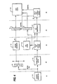
- An embodiment of the present invention used with a vector processor is illustrated in Figure 1. A load/
store pipeline 8 for the processor has five stages. These stages manage pipe entries propagating through the pipeline. Anaddress generator 10 receives commands from avector controller 6 and generates from these commands pipe entries. A pipe entry contains all of the information needed to initiate a transaction between processors or a processor and main memory such as address, element number, byte mask, validity bit, etc. Such transactions are carried out over anexternal bus 50. - Specifically, an exemplary embodiment of a pipe entry will contain the following bits. Kind bits <2:0> tell each of the five stages what mode to be in for that particular pipe entry. These modes include the "normal" mode (either a load or a store), an invalidate mode, or a read (fill) mode. Element bits <5:0> define which element is being loaded or stored. A valid bit informs as to the validity of the pipe entry. A last bit tells when the pipe entry is the last pipe entry of an instruction. The "don't cache" bit is used in cache fills, and causes the pipeline to not validate the cache, but just put the element into a vector register file. The physical address bits <29:0> correspond to the physical address of the data element in the main memory. Longword mask bits <7:0> contain the information needed to know which elements within a hexaword (to be defined later) are to be loaded or stored.
- The pipe entry from the
address generator 10 contains a virtual address. Atranslation buffer 2 receives the virtual address and translates it into a physical address. From thetranslation buffer 12, the pipe entry (which now contains a physical address) enters a cache tag look upstage 14. This look upstage 14 parses the physical address into a cache index and tag compare data. Thelookup stage 14 sends the cache index of a cache location to atag store 34. Thetag store 34 is a store of tags for entries in adata cache 38. The tag is made up of a portion of the bits of a physical address. Each block of data in thedata cache 38 has an associated tag. - The tag portion of the physical address (the tag compare data) is compared with the tag data (located in the tag store 34) for the cache location accessed by this physical address. The comparison is done by a
comparator 16. A hit signal is output by thecomparator 16 if the tags match, while a miss signal is output if they do not match. The cache index has also been sent by the cache tag look upstage 14 to thedata cache 38. In order to know the results of the tag comparison before a decision to write to thedata cache 38 is made, adelay stage 35 is interposed between the cache tag look upstage 14 and thedata cache 38. - The pipe entry and a hit or miss signal is then sent to the cache
data storage stage 18. At this time, thedata cache 38 has the physical address of a cache location and will either read data from or write data to that location, as long as there is a hit signal at the cachedata storage stage 18. Thedata cache 38 is connected to acache data bus 40 via alatch 19. Vector register files 42 which use the data from thecache 38 are also coupled to thecache data bus 40. - When the tags are matched by the
tag comparator 16, a hit signal is generated and the data is either driven by the cachedata storage stage 18, fromlatch 19 coupled to thedata cache 38 onto thecache data bus 40, or is driven from avector register file 42 onto thecache data bus 40 to be stored in thedata cache 38. If the tags do not match, the data is still driven but it is ignored by thedata cache 38 or theregister file 42. - A pipeline entry propagates through one stage every clock cycle, so that a single pipe entry will pass through the pipeline in five cycles. In a vector processor according to the invention, the load/store commands, and hence the pipe entries, are pipelined. This means that a second pipe entry will follow a first pipe entry into the load/
store pipeline 8 before the first entry completely passes through thepipeline 8. In the embodiment of Figure 1, the pipelining is such that during the normal course of operation, all of the five stages at any one time can contain successive pipe entries. - The load/
store pipeline 8 operates in one of three modes, as determined by a load/store controller 52. These modes are the load mode, the store mode and the cache fill mode. In the load mode, data is loaded from thedata cache 38 to avector register 42. During a store mode, data is conditionally stored into thedata cache 38 from avector register 42 depending whether the data misses or hits. The cache fill mode will be described later. The load/store controller sends out signals to the pipeline stages which inform the stages what mode the pipeline is to be in. - In order to access each particular location in a
vector register file 42, a register file address (RFA) is sent to thevector register file 42 from certain points in thepipeline 8. The RFA is a portion of bits (for example, six) of each pipe entry. With these bits, thevector register file 42 will know where it is to store data coming from thecache 38 in a load operation, or from where data in thefile 42 is to be retrieved to send to thecache 38 in a store operation. - The points in the pipeline at which the RFA is "tapped" off and sent to a
vector register file 42 are different, depending on the type of operation. This is due to the different cache data bus timing required for each operation. The timing for the various operations will be described in more detail later with reference to Figures 2-4. For now, it is sufficient to say that for a store operation, the RFA is tapped off after theaddress generator stage 10; at thetag comparator stage 16 for a cache fill operation; and after the cachedata storage stage 18 for a load operation. The RFA after each of these stages is sent to amultiplexer 51, which selects the appropriate RFA input line depending on a control signal from the load/store controller 2. The appropriate RFA is output by themultiplexer 51 to adelay latch 53 and from there, to the vector register files 42. - During a load operation, no problems arise if all of the tags match so that all of the cache requests are hits. However, sometimes there will be cache misses (when the tags do not match), indicating that there is no valid data at the specified physical address in the
data cache 38. These cache misses must be serviced so that the requested data can eventually be read from thecache 38. The servicing of a read miss during a load operation includes obtaining the requested data from another processor or main memory via theexternal bus 50. The requested data is filled into thedata cache 38 at the specified physical address and then driven onto thecache data bus 40 to thevector register file 42. - The above servicing of a miss can be performed in different ways. A relatively slow method is to stop the pipeline upon a read miss, fetch the data over the
external bus 50, fill the data to thecache 38 and then restart the pipeline. Such a method would be used when the cache is not part of the pipeline. The speed of this method is limited by the speed with which theexternal bus 50 can get the requested data to thecache 38. Until then, no other loads would be performed. - The present invention avoids this limitation by servicing a read miss while the pipeline is still operating (performing loads). The invention is implemented using read
miss buffers 26a-d. Although four readmiss buffers 26a-d are illustrated in Figure 1, any number of read miss buffers could be used. Upon receiving a miss signal during a load operation, the cachedata storage stage 18 does not drive data from thecache 38 onto thecache data bus 40. Instead, thecache data stage 18 sends a command address in the pipe entry to an available readmiss buffer 26a via a load/store internalcommand address bus 45. Assuming that successive pipe entries are hits, the loading from thecache 38 continues while the readmiss buffer 26a is being filled with data from the main memory viaexternal bus 50 as described below. - Each read
miss buffer 26a-d contains buffers for holding the command address of the pipe entry and a number of data elements corresponding to that command address, four for example. Anexternal bus controller 58 requests the data elements from main memory for a buffer which receives a command address. As the data elements are received over theexternal bus 50, theexternal bus controller 58 fills the data into the data buffers in the corresponding readmiss buffer 26a-d. When aread miss buffer 26a-d is completely filled, an internal flag is set, which indicates to the load/store controller 52 that data can be filled to thecache 38. - In similar fashion, the other three read
miss buffers 26b-d will be serviced when there are three more read misses. It is only after there have been four read misses so that there are no more available read miss buffers that the load/store pipeline 8 is stalled by the load/store controller 52. The load/store controller 52 now causes thepipeline 8 to enter the cache fill mode. Processing is suspended for all the pipe entries currently active in the pipeline. Instead, when the readmiss buffer 26a which received the first command address which missed has received the data from theexternal bus 50, the command address stored in thebuffer 26a is sent over thecommand address bus 45 to the cache tag look upstage 14 and is allocated as valid in thetag store 34, since thepipeline 8 is in the cache fill mode. The load/store controller 52 drives the data from the readmiss buffer 26a onto a load/storeinternal data bus 47, through alatch 20, and onto thecache data bus 40. The data is loaded into the appropriatevector register file 42, as indicated by the cache fill RFA. The data is then written through thelatch 19 into thedata cache 38. Theaddress generator 10 has backed up to regenerate those pipe entries which followed the pipe entry which caused the last miss, in this case the fourth miss. - In the embodiment, the
pipeline 8 then continues processing as before since at least one emptyread miss buffer 26a-d now exists. Thepipeline 8 will again be halted and the above procedures repeated when another read miss occurs so that readmiss buffer 26a will again be unavailable. However, instead of filling the cache from the readmiss buffer 26a, the read miss buffer, for example 26b, which received the second read miss command address is the buffer which fills thedata cache 38. In other words, theread miss buffers 26a-d will fill thedata cache 38, when called upon, in the order in which read misses were assigned to the buffers in a round-robin, FIFO order. - In the illustrated embodiment, the fill operation takes place in the order of buffer allocation. Other implementations may fill in different orders. After the vector has been completely scanned, in order to complete the load operation, the
cache 38 is filled from the readmiss buffers 26a-d with the requested data when this data becomes available. This data is driven onto the load/store data bus 47 andcache data bus 40 to thevector register 42. After all the requested data has been filled to thecache 38 and loaded to thevector register 42, the load operation is complete. - Storing data from the
vector register 42 into thedata cache 38 is not as involved. Thedata cache 38 is only changed during a store operation when there is a hit in thetag comparator 16. If there is a cache miss, thedata cache 38 remains unchanged. The only consequence of this is that when data is to be loaded from thedata cache 38 to thevector register 42 in a load operation, a miss will occur with the miss being serviced as described earlier. For coherency reasons, it is important that the rest of the system knows what is in thedata cache 38 at any time. For this purpose, during a store operation, a command address is sent to anaddress FIFO 54, and the data from thevector register file 42 corresponding to that command address is sent to adata FIFO 56. From these FIFO's 54, 56, the address and data are put onto theexternal bus 50, through theexternal bus controller 58 and sent to the system. The above description is for direct mapped write-through data cache. Other embodiments can handle write-back data caches. - The FIFO's 54, 56 are of a size such that they can take one complete vector store operation. This allows the
pipeline 8 to be used for a simultaneous load operation. One embodiment has the load operation wait for the store operation to complete if a read miss occurs during the load operation. Should there be a translation buffer miss during the store operation, the store operation will be stopped and the read miss serviced over theexternal bus 50. In other words, the translation buffer miss operation has priority over the store operation in the use of theexternal bus 50. - The invention has been described for ease of explanation using pipe entries which represent individual quadword eight contiguous byte) elements. However, in the illustrated embodiment, a single pipe entry represents four aligned quadword elements (a hexaword). In this case, the pipe entry is decomposed in the cache tag look up
stage 14 into its component quadwords, these quadword addresses being fetched one at a time from thedata cache 38. Since only one quadword per cycle can be delivered from thedata cache 38, theaddress generator 10 is stalled during the decomposition until the last quadword of the hexaword is reached. If there is a read miss, then the entire hexaword will be retrieved and eventually filled to theread miss buffers 26a-d and thedata cache 38. An example of a hexaword is shown in Figure 13. Note that in this example, the hexaword is not aligned. In other words,longword 1 is not on the left, so that the first quadword, containinglongwords address generator 10 allow the information to be properly written into the vector registers 42. - The use of the
read miss buffers 26a-d to obtain four quadwords at a time speeds the loading process since all of the aligned quadwords within the hexaword would miss if any one of the quadwords missed. - Another embodiment loads single quadword elements on hits, but after a read miss, will retrieve a hexaword to which the quadword that missed belonged. During the cache fill, the hexaword is decomposed, but only the quadword that missed is loaded into the
vector register file 42, while the entire hexaword is filled into thecache 38. - A cycle type (CT) is also part of the pipe entry, and informs the vector register files 42 what type of element is being used, such as a quadword or longword and the alignment of the longword within that quadword. The pipe entry data can be double precision numbers (a quadword) or two longwords (single precision floating point) or integer numbers. Due to physical alignments of the longwords in main memory, the load/store unit can request the vector registers 42 to transmit or receive data with the desired longword in the upper or lower longword of the quadword. This is specified by the CT. The CT is tapped off the
pipeline 8 at the same locations as the RFA. - As mentioned earlier, the RFA is tapped off the
pipeline 8 at different stages depending on what mode thepipeline 8 is in. Figures 2-4 show some of the components of Figure 1, reconfigured for purposes of explanation in the drawing to show the timing of the various operations. - Figure 2 illustrates the pipeline configuration for the load operation, where data is loaded from the cache to the
vector register 42. In stage 1L, theaddress generator stage 10 generates a virtual address. Thetranslation buffer 12 translates the virtual address instage 2L, and the physical cache tag data is looked up instage 3L. The tag comparison is done instage 4L, and data is driven out of thedata cache 38 instage 5L into thelatch 19, and the RFA is tapped out of the cachedata storage stage 18. In stage 6L, the RFA and the data are driven intolatches stage 7L, the RFA and the data are driven into the vector register files 42. Note that to satisfy electrical and timing constraints, latches can be used before thedata cache 38 and the cachedata store stage 18. Such latches would prevent timing race and loading conditions, as one skilled in the art would readily appreciate. - The pipeline configuration for the cache fill operation is shown in Figure 3. In stage 1CF, the command address which is to be filled is driven from one of the
read miss buffers 26a-d (e.g. 26a) onto thecommand address bus 45. During stage 2CF, the data which was filled into the readmiss buffer 26a is driven onto the load/storeinternal data bus 47. The tag for that command address is written into thetag store 34 by thecache tag lookup 14, which acts as an allocator in the cache fill mode. The RFA is driven out of the cachetag lookup stage 14. In stage 3CF, the data and the RFA are latched, as is the pipe entry by thetag comparator 16 which is acting as a latch and not a comparator in this mode. During stage 4CF, the data on theinternal data bus 47 is driven onto thecache data bus 40 and into the vector register files 42. The RFA is also driven to the vector register files 42 at this time. Finally, in stage 5CF, the data is latched, and driven onto thecache data bus 40 and into thedata cache 38. - The configuration for stores is shown in Figure 4. In
stage 1S, the virtual address is generated and the RFA is driven out of theaddress generator stage 10. Duringstage 2S, the virtual address is translated into a physical address, and the RFA is driven on thecache data bus 40 to the vector register files 42. Because of an inherent two cycle delay, data will appear two cycles later. The physical cache tag data is looked up instage 3S. Instage 4S, the tag data and the tag compare data are compared, and the vector register files 42 drives the data designated by the RFA onto thecache data bus 40 and latched inlatch 19. This data is driven into thedata cache 38 duringstage 5S. The data is written into thedata cache 38 if there is a cache hit, and is ignored if there is a cache miss. - Although Figures 2-4 show the various components of Figure 1 arranged in different positions, note that the couplings between the components are the same as in Figure 1. The reconfigurations are merely aids for understanding the timing and operation of the embodiment of Figure 1 in the three different operating modes. The "reconfiguring" is done by the
controller 6 sending control signals to the various components. - The timing diagrams shown in Figures 5-11 described below illustrate some examples of operation of the invention according to the principles of the invention discussed above.
- Referring to Figure 5 there is shown a timing chart for a load operation in the load/store pipeline. The pipeline stage configuration for a load operation is shown in Figure 2. The timing chart illustrates a six element load operation. For purposes of Figure 5, it is assumed that the
cache tag comparator 16 will always generate a match or hit. This particular vector load instruction is a six element load instruction transferring eight bytes of information per element. - The load/
store pipeline 8 functions by inputting a command or vector instruction into theaddress generator 10 as shown in Figure 5 at time t₀. Theaddress generator 10 decomposes the vector instruction into an efficient sequence of external bus transactions that will complete the instruction. The output from theaddress generator 10 is called a pipe entry. All the remaining stages of the load/store pipeline receive and transmit pipe entries. As shown in Figure 5, the address generated for the pipe entry at time t₀ is 408 (hex) forelement 0. The pipeline is in a normal mode for a quadword load operation. - At time t₁,
element 0 is passed through the pipe to thetranslation buffer 12 as shown byarrow 60. The virtual address from theaddress generator stage 10 is translated to a physical address by thetranslation buffer 12. - Due to the nature of a pipeline, the
next element 1 enters theaddress generator stage 10 of the pipe at time t₁. Again, the address generator stage decomposes the vector instruction into transactions that will complete the vector instruction. The output of theaddress generator stage 10 forelement 1 is a complete external bus transaction having virtual addresses. - At time t₂,
element 0 is shifted from thetranslation buffer 12 into the cache tag look upstage 14 as shown byarrow 61. The cache tag look upstage 14 looks up the tag in thetag store 34 for the physical address and returns it to thecache tag comparator 16.Element 0 is transferred to thecache tag comparator 16 at time t₃ where the tag compare is performed. Assuming in Figure 5 that all cache compares generate a match or hit,element 0 is read in thedata cache 38 at time t₄ as shown byarrow 63 and illustrated in Figure 2. The data is then driven out of thedata cache 38 into thelatch 19 to be placed on thecache data bus 40. Also at time t₄, the RFA is driven out of the cachedata store stage 18 into alatch 62. - At time t₅, the RFA/CT is driven from the
latch 62 onto thecache data bus 40 as shown byarrow 64. Further, the data forelement 0 is driven fromlatch 19 onto thecache data bus 40 and the cache data bus is instructed to write the vector registers 42 thus completing the load operation forelement 0. - Returning to time t₂, it is seen that
element 1 is passed from theaddress generator 10 to thetranslation buffer 12 as shown byarrow 65. Further,element 2 now enters theaddress generator 10 of the pipeline. -
Element 1 is shifted through thestages read miss buffers 26a-d are therefore not utilized when thecache tag comparator 16 does not generate a miss. - Referring to Figures 6-6c in conjunction with Figures 2 and 3, there is shown an eight element vector quadword load operation wherein cache miss signals are generated in the
cache tag comparator 16. In operation, at time t₀,element 0 enters theaddress generator 10. The operation of theaddress generator 10 is the same as described above in the vector load operation of Figure 5.Element 0 passes through the pipe at time t₁ to thetranslation buffer stage 12 as shown byarrow 80.Element 0 continues to transfer stages as shown byarrows stage 14 into thecache tag comparator 16. Again, the operation of the load pipeline is the same as described above. - However, at time t₃ the
cache tag comparator 16 performs a tag compare which results in a cache miss. Therefore, as seen fromblock 83, the command/address forelement 0 is loaded into the first of the four readmiss buffers 26a-d over the load/store internalcommand address bus 45. - The subsequent pipe entries, elements 1-3, pass through the pipe in order until each element generates a cache miss in the
cache tag comparator 16. Each cache miss loads the command address of the pipe entry sequentially into one of the four readmiss buffers 26a-d through thecommand address bus 45 as shown in the timing chart by blocks 90-92. As can be seen from the timing chart at time t₆, all four of theread miss buffers 26a-d are filled. However,elements block 89 by thecache tag comparator 16. - The pipe entry elements 0-3 in the
read miss buffers 26a-d are serviced by theexternal bus 58 which fetches the cache fill information from memory. Because the pipeline queues the four read misses into theread miss buffers 26a-d in the four successive clock ticks, there are no longer any read miss buffers available for the pipeline to use should another read miss occur. However, as indicated above, there are three vector element addresses already started in the pipeline that have not been processed. - As indicated at time t₇ and t₈, the
pipeline 8 must therefore halt while theread miss buffers 26a-d are serviced by theexternal bus 58. Theaddress generator 10 will back up to the pipe entry element following the pipe entry element which caused the fourth cache miss. - Time t₉ shows the holding of
pipe element 5 in theaddress generator 10 as indicated byblock 93. At the same time t₉,element 4 is on hold in thetranslation buffer 12 as indicated byblock 94. - Once the first
read miss buffer 26a has been serviced by theexternal bus 58, the data information is available on thecommand address bus 45 as indicated byblock 95 forelement 0. At time t₁₀, the pipeline continues withelement 5 in theaddress generator 10 andelement 4 recording a hit in thetranslation buffer 12, as indicated byblocks command address bus 45 and all read miss buffers are filled, the pipeline is changed into the cache fill mode and the physical address for the cache fill is sent to the cachetag lookup stage 14 as shown inblock 98. Also as indicated inblock 98, the address is allocated and validated in thelookup stage 14. At the same time, the data is available on theinternal data bus 47 as shown inblock 200. - Continuing at time t₁₁, block 99 indicates that
element 6 is ready in theaddress generator 10. In the next stage down the pipeline,element 5 records a hit in thetranslation buffer 12 as shown byblock 100. Further, the cache tag lookup onelement 4 is performed in thecache lookup stage 14 as shown byblock 101. Thecache tag comparator 16, indicated byblock 102, now receives the cache fill ofelement 0 as shown byblock 102. At the same time, thecache data bus 40 receives the fill data from theinternal data bus 47 as shown inblock 103. Further, the fill RFA and CT are driven onto thecache data bus 40. - At time t₁₂ the
final element 7 enters theaddress generator 10. Further,elements load pipeline 8 as shown byblocks element 4 encounters a cache miss in thecache tag comparator 16 as shown byblock 107. As was done previously, the cache miss loads the available readmiss buffer 26a by using thecommand address bus 45 as indicated byblock 109. At the same time t₁₂, thedata cache 38 is written with the information fromelement 0 which was on thecache data bus 40 from the read miss buffers as indicated inblock 108. - As can be seen from Figures 6 and 6A, the four read
miss buffers 26a-d are again filled and thus the load pipeline must drain, hold and back up toelement 5 as shown at times t₁₃ and t₁₄. The term "drain" means the permitting of all stages of the pipeline to complete their operation. At time t₁₄,element 6 is holding in theaddress generator 10 andelement 5 is holding in thetranslation buffer 12 as shown byblocks -
Block 112 indicates that thecommand address bus 45 now has available the information for servicingelement 1 which was the second element placed in one of theread miss buffers 26a-d. At time t₁₅, therefore, thepipeline 8 continues withelement 6 in theaddress generator 10 andelement 5 recording a hit in thetranslation buffer 12 as indicated byblocks element 1 which was serviced by theexternal bus 50 is now available on theinternal data bus 47 as shown byblock 116. The address is input to thecache tag comparator 16 from thecommand address bus 45 as shown byblock 115. The allocation and validation process is performed by thecache tag lookup 14. Continuing at time t₁₆, apipe entry element 7 again enters theaddress generator 10 of thepipeline 8. Further,element 6 records a hit in thetranslation buffer 12 andelement 5 has the cache tag look upstage 14 perform a tag lookup. At time t₁₆, thecache tag comparator 16 receives the cache fill ofelement 1 as shown byblock 117. Further, thecache data bus 40 now has the data and RFA/CT forelement 1 available on thebus 40 for writing the vector registers 42. - At time t₁₇, as shown in
block 119, thedata cache 38 haselement 1 written to it, so as to complete the cache fill for that element. At the same time,element 5 passes from the cachetag lookup stage 14 to thecache tag comparator 16 where a cache miss is generated as shown inblock 120. Again, the cache miss ofelement 5 is loaded into one of the available readmiss buffers 26a-d through thecommand address bus 45 as seen inblock 121. - This sequence of running the load pipeline and servicing the cache fills continues in the pipe until the
final element 7 encounters a cache miss in thecache tag comparator 16 as shown at time t₂₉ by block 122 (Figure 6B). At time t₂₉, the cache miss inelement 7 loads one of the available readmiss buffers 26a-d through the load/store internalcommand address bus 45 as shown inblock 123. At the same time, as shown inblock 124,element 3 is written into thedata cache 38 from thecache data bus 40 as was done previously for elements 0-2. - Because the
read miss buffers 26a-d are again filled, the load pipeline drains, holds and backs up as shown illustratively at times t₃₀ and t₃₁. Finally, at time t₃₂,element 4 has been serviced by theexternal bus 50 and is ready to return to the pipeline as is illustrated at times t₃₃-t₃₅.Element 4 has its cache miss filled as was done previously for the earlier elements. Because no further elements are loaded into theaddress generator 10 for the vector instruction, thepipeline 8 remains in a cache fill mode to service the remaining read miss buffers until the entire load is completed (Figure 6C). - An alternative embodiment for a non-unity stride vector load operation is shown in Figures 7-7D. The timing charts of Figures 7-7D illustrate a six element load operation where each element encounters a cache miss. The load operation is performed substantially as described above for Figures 6-6C. However, after the fourth cache miss which fills the read miss buffers, as shown by blocks 202-208 (Figure 7), the cache fill mode operates differently than described above.
- In operation, the cache fill mode has available the command address on the
command address bus 45 as shown inblock 210 at time t₁₀ (Figure 7A). At time t₁₁, the address is input to the cachetag lookup stage 14 for allocation and validation. - The embodiment of Figures 7-7D returns a hexaword of information into the read miss buffers rather than the single quadword described above in Figures 6-6C. Therefore, although only a single quadword is needed for the non-unity stride operation, the cache tag lookup stage must decompose the hexaword address into its four quadwords as shown during times t₁₂ to t₁₄. During the decomposition time, the
address generator 10 andtranslation buffer 12 stages of the pipeline hold until the final decomposition at time t₁₄. - The data for each quadword is sequentially driven onto the
internal data bus 47 as shown by blocks 212-218. On the following clock tick, the data is driven onto thecache data bus 40 as shown during times t₁₂ to t₁₅. At the same times, t₁₂ to t₁₅, the RFA/CT is driven onto thecache data bus 40. Because only a single quadword is necessary, the RFA and CT are only valid for one quadword out of the hexaword. This is shown forelement 0 having thevalid quadword address 408, at time t₁₃. On the next clock tick, t₁₄, thedata cache 38 is written with the fill data. - This process continues as described above for all of the elements in the load operation. Figures 7-7D allow a hexaword of information to be fetched by the external bus even though only a single quadword is necessary.
- Referring to Figure 8 in conjunction with Figure 4, there is shown a timing chart for a vector store operation having eight elements. The operation of Figure 8 begins with the
address generator 10 producing a sequence of pipe entries starting withelement 0 as shown inblock 140 at time t₀.Element 0 passes down the pipeline to thetranslation buffer 12 as shown byarrow 141 at time t₁. The virtual address from theaddress generator 10 is translated to a physical address in thetranslation buffer 12. At the same time, the RFA/CT is driven onto thecache data bus 40 as shown inblock 222. The store operation reads the data from the vector registers 42. - The physical address is then driven into the cache
tag lookup stage 14 as shown byarrow 143 at time t₂. The cache tag is looked up and theelement 0 passes to thecache tag comparator 16 as shown byarrow 145 at time t₃. Also at time t₃, the vector registers 42 drives the data onto thecache data bus 40 as shown byblock 224. Thecache tag comparator 16 performs a tag compare as shown byblock 146. Finally, at time t₄, the data is driven from thecache data bus 40 and written into thedata cache 38 as shown byblock 148 when the tag compare, block 146, results in a cache hit. However, if the tag compare results in a cache miss, the cache is unchanged. This operation continues for the entire store operation as shown in Figure 8. - Referring to Figures 9 and 9A, there is shown a timing diagram for a vector load operation having a unity stride. When the stride is unity, the vector elements are stored contiguously in memory. Therefore, each pipe entry produced by the
address generator stage 10 represents multiple elements. This takes advantage of the higher external bus bandwidth available when accessing contiguous memory locations. Figures 9 and 9A viewed in conjunction with Figure 2 shows a five hexaword vector operation loading seventeen elements where it is assumed that thecache tag comparator 16 continuously generates a match. - In general, the operation of the load/
store pipeline 8 for a unity stride operation is the same as for a non-unity stride operation as described above. However, theaddress generator 10 can produce a sequence of pipe entries beginning withelement 0. Each pipe entry may represent between 1 and 4 elements (i.e., a hexaword). This is shown in the timing chart ataddress generator 10 where the elements entering theaddress generator 10 are multiples of four. Thus, the element count is incremented by four for every pipe entry. - As was done previously, each virtual address from the
address generator 10 is translated to a physical address in thetranslation buffer 12. Next, the physical address is passed to the cachetag lookup stage 14 and then to thecache tag comparator 16. A tag compare is performed in thecache tag comparator 16 which, for purposes of Figure 9, always will result in a cache hit. The block size of the cache is one hexaword; a cache hit indicates that the entire hexaword (all elements contained in the pipe entry) is in the cache. - It is noted that the pipe entry is composed of four sub elements (or quadwords) in Figure 9. The cache, however, can only deliver one sub element per clock tick. Therefore, as shown during time t₂-t₅, the pipe entry contained in the cache
tag lookup stage 14 must be decomposed into its component sub elements and these sub element addresses are then read from thedata cache 38. The sub elements read from thedata cache 38 are driven onto thecache data bus 40 and written into the vector registers. While the pipe entry is being decomposed in the cachetag lookup stage 14, theaddress generator 10 of the pipe is stalled at the next hexaword address (t₁). Thegenerator 10 remains stalled until the last sub element of the hexaword is reached. - It is important to note from Figure 9 that the pipe entry decomposition in the cache
tag lookup stage 14 begins before the results of the cache lookup are known in thecache tag comparator 16. Decomposition begins unconditionally and it is assumed that the cache will hit. After the last element has been loaded from thedata cache 38, its parity is checked. If the parity is correct, the load/store chip notifies the vector controller that the vector load operation is complete. - Referring to Figures 10-10D, there is shown a unity stride timing chart for a six hexaword vector operation loading twenty-two elements. It is assumed in Figures 10-10D that the cache tag comparison will always result in a cache miss. The operation of Figures 10-10D, viewed in conjunction with Figures 2 and 3, for a unity stride vector load operation is similar to that for the non-unity stride operation illustrated in Figures 7-7D.
- The initial operation of Figures 10-10D, i.e. t₀-t₂ is the same as that for Figure 9. However, unlike Figure 9 which always generates tag hits, the tag compare performed in the
cache tag comparator 16 of Figure 10 always results in a cache miss. The cache miss loads the pipe entry into one of theread miss buffers 26a-d by thecommand address bus 45, block 230(t₄), for servicing by theexternal bus 58. The decomposition started in the cachetag lookup stage 14, block 232(t₃), is aborted when this occurs and the resulting pipe entry is ignored as shown in block 234(t₄). Theaddress generator 10 which was stalled when the decomposition started is now released from the stalled condition and produces a new pipe entry when the miss is loaded into the read miss buffer. This operation continues until all four readmiss buffers 26a-d are loaded by thecommand address bus 45, block 236, at time t₁₃. - Because there are no more read miss buffers available should another read miss occur, the pipeline must halt and the
address generator 10 must back up to the pipe entry following the pipe entry causing the fourth cache miss. The generation of pipe entries will eventually be restarted at this point. - While the pipeline is halted, the
address generator 10 andtranslation buffer 12 stall, t₁₅-t₁₈ (Figure 10A), until the first read miss buffer has been serviced the command address being available on thecommand address bus 45. The command address is used to service the cache fill. Once theexternal bus 58 has serviced the read miss buffer, the pipe entry from the read miss buffer is delivered to the cachetag lookup stage 14 of the pipe by thecommand address bus 45 as shown at time t₁₆. The cache fill data is driven onto the load/storeinternal data bus 47 at the same time. - The mode of the pipeline is changed to the cache fill mode by the
pipe controller 52. The tag is allocated and validated in thetag store 34 by thetag lookup 14. As shown in Figure 10A at time t₁₇, the pipe entry in thecache tag comparator 16 is now decomposed into its four component sub elements. The four sub elements of the returned hexaword are driven onto thecache data bus 40 during times t₁₇-t₂₀. The data is written into thedata cache 38 during times t₁₈-t₂₁. - After the first cache fill service completes the decomposition at time t₁₉, the
pipe controller 52 releases theaddress generator 10 of the pipe as a read miss buffer is now available if another cache miss occurs. At time t₂₁, another cache miss occurs thus filling the fourth read miss buffer at time t₂₂. The pipeline is again halted, backed up and stalled until the next read miss buffer is serviced. This operation continues until all of the elements have been processed. If no further misses occur, the read miss buffers are serviced after all the other elements have been processed through the pipeline. - After the last element has been loaded, and all of the sub elements (quadwords) of the last hexaword fill are complete, the
vector controller 6 is notified that the vector load of unity stride is complete. - Figure 11 shows a timing chart for a seven hexaword vector store operation having a unity stride. The operation of Figure 11 is the same as that of Figure 8 for a non-unity stride store operation.
- An embodiment of a pipeline with an integral cache for use in a scalar processor according to the present invention is illustrated in Figure 12. The
reference numeral 200 refers to the entire pipeline. Theissuer 210 provides a displacement value and control signals depending on the type of instruction, e.g. a load instruction or a store instruction. Aregister file 212 stores results from an arithmetic logic unit (ALU) 216 and has two write ports and two read ports. - The displacement value from the
issuer 210 is added to a base address from theregister file 212 by theALU 216 to produce a virtual address. Such a virtual address can be thirty-two bits for example. The thirty-two bits of virtual address (VA<31:0>) are presented simultaneously to a translation buffer (TB) 218 and a cache tag look up 220 although thecache tag lookup 220 only uses eight bits (VA<10:3>) to index a tag. Thetranslation buffer 218 and cache tag look up 220 each send twenty-one physical address bits (PA<31:11>) to thecomparator 224 which produces a hit signal when the bits match or a miss signal when there is a mismatch. The eight bits which are sent to the cache tag look up 220 are the untranslated bits of the virtual address VA<31:0>. Thus, no translation mechanism is necessary in front of the cache tag look up 220, and the tag lookup, address translation and comparison can be done within one cycle. The use of only eight untranslated bits to index the tag is allowed due to the size of the data cache and the page size used in the system. - A
controller 222 receives the hit/miss signal from thecomparator 224, and will cause the data to be written in or read from thedata cache 226 if there is a hit. Alatch 252 receives the bits VA<10:3> so that the data cache is indexed one cycle after the comparison. If there is a hit, data is written into the cache (in a store operation) or read from the cache (in a load operation). Due to the cache load or store being performed serially after the comparison, there is an equal number of stages in the pipeline for both the load operation and the store operation. - When there is a miss signal, the entire physical address (PA<31:0>) is sent to an
output fifo 228 which is connected to the main memory system of the scalar processor. The address is then sent from theoutput fifo 228 in order to fetch the data from the main memory. At the same time, the physical address is sent to amemory reference tag 230, which in the illustrated embodiment, has four locations which each store a physical address (PA), a register file number (RF#) and the data length (DL). - It should be noted that control information has been passed down the pipe along with the address, although it has not been shown for purposes of illustration. Some of this information is the register file number which determines where in the register file data is written to; and the data length, which tells the
register file 212 what part of the returning data is to be input to theregister file 212. - In the embodiment shown in Figure 12, the
output fifo 228 has eight locations and thememory reference tag 230 has four locations. Thus, during a load operation, up to four load misses can be put into thememory reference tag 230. When another load miss occurs while thememory reference tag 230 is full, no-ops are sent by theissuer 210 until data has been returned over theexternal bus 250. - When the data is returned, it enters a
buffer 236 which sends the data to both the data cache 226 (through multiplexer 238) and theregister file 212. The corresponding RF# and DL are sent from thememory reference tag 230 to theregister file 212 so that the returned data can be properly written into theregister file 212. The physical address (PA<31:0>) is sent to thecache tag lookup 220 and at the indexed location (PA<10:3>), bits PA<31:11> (the tag) will be written so that the next lookup to that tag location will be valid. - Because the
data cache 226 is a write-through cache, during write operations in which thedata cache 226 is being changed, the rest of the system must know what is in thedata cache 226. For this reason, buffers 234A-C are coupled between theregister file 212 and theoutput fifo 228 and pass the data out through theoutput fifo 228 during every store operation. - During a load operation, when there is a miss, the output fifo provides information to the processor indicating that there is a load operation, the size of the data element requested, the physical address where the data element is located in the main memory of the processor and the tag which is used by the pipeline.
- For a store operation the information which is output by the
output fifo 228 is the fact that it is a store operation, the size of the data element, the physical address and the data element itself. - Due to the operation of the
fifo 228 and thememory reference tag 230, thepipeline 200 of Figure 12 can support multiple outstanding misses while continuing to operate. In order to continue the pipeline subsequent to a cache miss, dependancy checks must be made. To that end, the controller provides for a write abort. Thus, if during a load operation there is a cache miss (so that thememory reference tag 230 contains a miss) which is followed by any store instruction, this subsequent store operation will be aborted. Alternatively, a procedure for checking the dependency between loads and stores is to compare, using a content addressable memory device, the physical address of the store instruction in theoutput fifo 228 with the physical address in thememory reference tag 230, and performing a write abort if any of the numbers match. A write abort includes aborting all the instructions currently in the pipeline and backing up the program counter in theissuer 210 to reissue all of the instructions subsequent to the last load instruction which missed and was put into thememory reference tag 230.
Claims (29)
a cache memory for storing data entries;
a data loading device which loads data entries from said cache memory to said registers and which stores data from said registers in said cache memory with loading and storing data entries to said cache memory being pipelined;
a determining device which determines when one of said entries is a miss;
read miss buffers coupled to said miss determining device which store command addresses associated with said missed data entries and obtaining data entries from out of said pipeline independently of the operation of said pipeline, said data entries corresponding to said command addresses; and
a filling device which fills the cache memory with said command address data entries and writes said command address data entries to said registers.
a cache memory for storing data;
a loading device which loads data entries from said cache memory to said registers and which stores data entries from said registers in said cache memory with loading and storing data entries to said cache memory being pipelined;
a determining device which determines when one of said data entries is a miss and which obtains return data entries from out of said pipeline independently of the operation of said pipeline when one of said data entries is a miss, said returned data entry corresponding to said missed data entry; and a filling device which fills the cache memory with said returned data entry.
an address generator operating to generate address information entries serially, each one of the address information entries relating to a corresponding one of a series of data entries;
a cache tag lookup and comparator device coupled to the address generator to receive the address information entries serially from the address generator and operating to perform a cache tag lookup and tag compare operation, serially, for each one of the address information entries; and
a data cache including a coupling to each of the address generator and the registers to receive the address information entries, serially, from the address generator and operating to selectively perform in respect of each of the data entries corresponding to the address information entries, one of a load of the each of the data entries from the cache memory to the registers and a store of each one of the data entries from the registers to the cache memory;
the coupling between the data cache and the address generator including a delay device operating to delay the receiving of each one of the address information entries by the data cache relative to the receiving of the each one of the address information entries by the cache tag lookup and comparator device by at least one cycle time.
Applications Claiming Priority (2)
| Application Number | Priority Date | Filing Date | Title |
|---|---|---|---|
| US07/224,483 US5148536A (en) | 1988-07-25 | 1988-07-25 | Pipeline having an integral cache which processes cache misses and loads data in parallel |
| US224483 | 1988-07-25 |
Publications (3)
| Publication Number | Publication Date |
|---|---|
| EP0352633A2 true EP0352633A2 (en) | 1990-01-31 |
| EP0352633A3 EP0352633A3 (en) | 1991-04-17 |
| EP0352633B1 EP0352633B1 (en) | 2000-06-14 |
Family
ID=22840901
Family Applications (1)
| Application Number | Title | Priority Date | Filing Date |
|---|---|---|---|
| EP89113324A Expired - Lifetime EP0352633B1 (en) | 1988-07-25 | 1989-07-20 | A pipeline having an integral cache for computer processors |
Country Status (6)
| Country | Link |
|---|---|
| US (2) | US5148536A (en) |
| EP (1) | EP0352633B1 (en) |
| JP (1) | JPH0290265A (en) |
| KR (1) | KR920004289B1 (en) |
| AT (1) | ATE193949T1 (en) |
| DE (1) | DE68929224T2 (en) |
Cited By (4)
| Publication number | Priority date | Publication date | Assignee | Title |
|---|---|---|---|---|
| EP0519685A1 (en) * | 1991-06-18 | 1992-12-23 | International Business Machines Corporation | Address translation |
| US6202506B1 (en) | 1996-05-14 | 2001-03-20 | Storck Bicycle Gmbh | Bicycle crank |
| WO2006089194A3 (en) * | 2005-02-17 | 2007-03-29 | Qualcomm Inc | Unaligned memory access prediction |
| US7447868B2 (en) | 2005-06-15 | 2008-11-04 | International Business Machines Corporation | Using vector processors to accelerate cache lookups |
Families Citing this family (91)
| Publication number | Priority date | Publication date | Assignee | Title |
|---|---|---|---|---|
| US5535359A (en) * | 1988-12-02 | 1996-07-09 | Mitsubishi Denki Kabushiki Kaisha | Computer system with cache memory having address mask register |
| JPH0666056B2 (en) * | 1989-10-12 | 1994-08-24 | 甲府日本電気株式会社 | Information processing system |
| US5317718A (en) * | 1990-03-27 | 1994-05-31 | Digital Equipment Corporation | Data processing system and method with prefetch buffers |
| JP2862948B2 (en) * | 1990-04-13 | 1999-03-03 | 三菱電機株式会社 | Semiconductor storage device |
| US5838946A (en) * | 1990-04-14 | 1998-11-17 | Sun Microsystems, Inc. | Method and apparatus for accomplishing processor read of selected information through a cache memory |
| US5432918A (en) * | 1990-06-29 | 1995-07-11 | Digital Equipment Corporation | Method and apparatus for ordering read and write operations using conflict bits in a write queue |
| US5404482A (en) * | 1990-06-29 | 1995-04-04 | Digital Equipment Corporation | Processor and method for preventing access to a locked memory block by recording a lock in a content addressable memory with outstanding cache fills |
| US5724548A (en) * | 1990-09-18 | 1998-03-03 | Fujitsu Limited | System including processor and cache memory and method of controlling the cache memory |
| JP2677706B2 (en) * | 1990-10-19 | 1997-11-17 | 富士通株式会社 | Memory access control circuit |
| JP2678527B2 (en) * | 1991-01-08 | 1997-11-17 | 三菱電機株式会社 | Cache memory device |
| US5265233A (en) * | 1991-05-17 | 1993-11-23 | Sun Microsystems, Inc. | Method and apparatus for providing total and partial store ordering for a memory in multi-processor system |
| JP2625277B2 (en) * | 1991-05-20 | 1997-07-02 | 富士通株式会社 | Memory access device |
| US5493687A (en) | 1991-07-08 | 1996-02-20 | Seiko Epson Corporation | RISC microprocessor architecture implementing multiple typed register sets |
| US5539911A (en) | 1991-07-08 | 1996-07-23 | Seiko Epson Corporation | High-performance, superscalar-based computer system with out-of-order instruction execution |
| US5386526A (en) * | 1991-10-18 | 1995-01-31 | Sun Microsystems, Inc. | Cache memory controller and method for reducing CPU idle time by fetching data during a cache fill |
| US5353424A (en) * | 1991-11-19 | 1994-10-04 | Digital Equipment Corporation | Fast tag compare and bank select in set associative cache |
| US5398330A (en) * | 1992-03-05 | 1995-03-14 | Seiko Epson Corporation | Register file backup queue |
| DE69311330T2 (en) | 1992-03-31 | 1997-09-25 | Seiko Epson Corp | COMMAND SEQUENCE PLANNING FROM A RISC SUPER SCALAR PROCESSOR |
| WO1993022722A1 (en) | 1992-05-01 | 1993-11-11 | Seiko Epson Corporation | A system and method for retiring instructions in a superscalar microprocessor |
| US5398325A (en) * | 1992-05-07 | 1995-03-14 | Sun Microsystems, Inc. | Methods and apparatus for improving cache consistency using a single copy of a cache tag memory in multiple processor computer systems |
| US6735685B1 (en) * | 1992-09-29 | 2004-05-11 | Seiko Epson Corporation | System and method for handling load and/or store operations in a superscalar microprocessor |
| JP3644959B2 (en) * | 1992-09-29 | 2005-05-11 | セイコーエプソン株式会社 | Microprocessor system |
| US5388226A (en) * | 1992-10-05 | 1995-02-07 | Motorola, Inc. | Method and apparatus for accessing a register in a data processing system |
| US5572714A (en) * | 1992-10-23 | 1996-11-05 | Matsushita Electric Industrial Co., Ltd. | Integrated circuit for pipeline data processing |
| JP3531166B2 (en) | 1992-12-31 | 2004-05-24 | セイコーエプソン株式会社 | Register renaming system and method |
| US5628021A (en) | 1992-12-31 | 1997-05-06 | Seiko Epson Corporation | System and method for assigning tags to control instruction processing in a superscalar processor |
| JP3230898B2 (en) * | 1993-06-02 | 2001-11-19 | シャープ株式会社 | Data driven information processing system |
| US5553270A (en) * | 1993-09-01 | 1996-09-03 | Digital Equipment Corporation | Apparatus for providing improved memory access in page mode access systems with pipelined cache access and main memory address replay |
| US6128721A (en) * | 1993-11-17 | 2000-10-03 | Sun Microsystems, Inc. | Temporary pipeline register file for a superpipelined superscalar processor |
| US5996062A (en) * | 1993-11-24 | 1999-11-30 | Intergraph Corporation | Method and apparatus for controlling an instruction pipeline in a data processing system |
| US5671444A (en) * | 1994-02-28 | 1997-09-23 | Intel Corporaiton | Methods and apparatus for caching data in a non-blocking manner using a plurality of fill buffers |
| DE69530720T2 (en) * | 1994-03-09 | 2003-11-27 | Sun Microsystems Inc | Delayed cache write of a save command |
| US6021471A (en) * | 1994-11-15 | 2000-02-01 | Advanced Micro Devices, Inc. | Multiple level cache control system with address and data pipelines |
| GB2290395B (en) | 1994-06-10 | 1997-05-28 | Advanced Risc Mach Ltd | Interoperability with multiple instruction sets |
| US5787465A (en) * | 1994-07-01 | 1998-07-28 | Digital Equipment Corporation | Destination indexed miss status holding registers |
| US5535360A (en) * | 1994-08-31 | 1996-07-09 | Vlsi Technology, Inc. | Digital computer system having an improved direct-mapped cache controller (with flag modification) for a CPU with address pipelining and method therefor |
| US5701433A (en) * | 1994-10-14 | 1997-12-23 | Compaq Computer Corporation | Computer system having a memory controller which performs readahead operations which can be aborted prior to completion |
| US5548728A (en) * | 1994-11-04 | 1996-08-20 | Canon Information Systems, Inc. | System for reducing bus contention using counter of outstanding acknowledgement in sending processor and issuing of acknowledgement signal by receiving processor to indicate available space in shared memory |
| US5699538A (en) * | 1994-12-09 | 1997-12-16 | International Business Machines Corporation | Efficient firm consistency support mechanisms in an out-of-order execution superscaler multiprocessor |
| US5890222A (en) * | 1995-01-04 | 1999-03-30 | International Business Machines Corporation | Method and system for addressing registers in a data processing unit in an indirect addressing mode |
| US5680338A (en) * | 1995-01-04 | 1997-10-21 | International Business Machines Corporation | Method and system for vector processing utilizing selected vector elements |
| US5887183A (en) * | 1995-01-04 | 1999-03-23 | International Business Machines Corporation | Method and system in a data processing system for loading and storing vectors in a plurality of modes |
| US5832533A (en) * | 1995-01-04 | 1998-11-03 | International Business Machines Corporation | Method and system for addressing registers in a data processing unit in an indexed addressing mode |
| JP3569811B2 (en) * | 1995-01-25 | 2004-09-29 | 株式会社ルネサステクノロジ | Data processing device having pipeline processing function |
| US5687350A (en) * | 1995-02-10 | 1997-11-11 | International Business Machines Corporation | Protocol and system for performing line-fill address during copy-back operation |
| JPH0934786A (en) * | 1995-07-14 | 1997-02-07 | Fujitsu Ltd | Instruction supplying device |
| US5924125A (en) * | 1995-08-01 | 1999-07-13 | Arya; Siamak | Method and apparatus for parallel access to consecutive TLB entries |
| US6076150A (en) * | 1995-08-10 | 2000-06-13 | Lsi Logic Corporation | Cache controller with improved instruction and data forwarding during refill operation |
| US5767856A (en) * | 1995-08-22 | 1998-06-16 | Rendition, Inc. | Pixel engine pipeline for a 3D graphics accelerator |
| US6101590A (en) | 1995-10-10 | 2000-08-08 | Micro Unity Systems Engineering, Inc. | Virtual memory system with local and global virtual address translation |
| US5809530A (en) * | 1995-11-13 | 1998-09-15 | Motorola, Inc. | Method and apparatus for processing multiple cache misses using reload folding and store merging |
| US5848287A (en) | 1996-02-20 | 1998-12-08 | Advanced Micro Devices, Inc. | Superscalar microprocessor including a reorder buffer which detects dependencies between accesses to a pair of caches |
| US5761720A (en) * | 1996-03-15 | 1998-06-02 | Rendition, Inc. | Pixel engine pipeline processor data caching mechanism |
| US5652774A (en) * | 1996-07-08 | 1997-07-29 | International Business Machines Corporation | Method and apparatus for decreasing the cycle times of a data processing system |
| US5802564A (en) * | 1996-07-08 | 1998-09-01 | International Business Machines Corp. | Method and apparatus for increasing processor performance |
| US6209020B1 (en) * | 1996-09-20 | 2001-03-27 | Nortel Networks Limited | Distributed pipeline memory architecture for a computer system with even and odd pids |
| US6088788A (en) * | 1996-12-27 | 2000-07-11 | International Business Machines Corporation | Background completion of instruction and associated fetch request in a multithread processor |
| US6085292A (en) * | 1997-06-05 | 2000-07-04 | Digital Equipment Corporation | Apparatus and method for providing non-blocking pipelined cache |
| US7197625B1 (en) * | 1997-10-09 | 2007-03-27 | Mips Technologies, Inc. | Alignment and ordering of vector elements for single instruction multiple data processing |
| US6567839B1 (en) | 1997-10-23 | 2003-05-20 | International Business Machines Corporation | Thread switch control in a multithreaded processor system |
| US6105051A (en) * | 1997-10-23 | 2000-08-15 | International Business Machines Corporation | Apparatus and method to guarantee forward progress in execution of threads in a multithreaded processor |
| US6076157A (en) * | 1997-10-23 | 2000-06-13 | International Business Machines Corporation | Method and apparatus to force a thread switch in a multithreaded processor |
| US6212544B1 (en) | 1997-10-23 | 2001-04-03 | International Business Machines Corporation | Altering thread priorities in a multithreaded processor |
| US6697935B1 (en) | 1997-10-23 | 2004-02-24 | International Business Machines Corporation | Method and apparatus for selecting thread switch events in a multithreaded processor |
| US6061710A (en) * | 1997-10-29 | 2000-05-09 | International Business Machines Corporation | Multithreaded processor incorporating a thread latch register for interrupt service new pending threads |
| US6256775B1 (en) | 1997-12-11 | 2001-07-03 | International Business Machines Corporation | Facilities for detailed software performance analysis in a multithreaded processor |
| US6018759A (en) * | 1997-12-22 | 2000-01-25 | International Business Machines Corporation | Thread switch tuning tool for optimal performance in a computer processor |
| US6148372A (en) * | 1998-01-21 | 2000-11-14 | Sun Microsystems, Inc. | Apparatus and method for detection and recovery from structural stalls in a multi-level non-blocking cache system |
| US6226713B1 (en) | 1998-01-21 | 2001-05-01 | Sun Microsystems, Inc. | Apparatus and method for queueing structures in a multi-level non-blocking cache subsystem |
| US6012134A (en) * | 1998-04-09 | 2000-01-04 | Institute For The Development Of Emerging Architectures, L.L.C. | High-performance processor with streaming buffer that facilitates prefetching of instructions |
| US6438650B1 (en) * | 1998-12-16 | 2002-08-20 | Intel Corporation | Method and apparatus for processing cache misses |
| US6437789B1 (en) | 1999-02-19 | 2002-08-20 | Evans & Sutherland Computer Corporation | Multi-level cache controller |
| US6237066B1 (en) | 1999-03-22 | 2001-05-22 | Sun Microsystems, Inc. | Supporting multiple outstanding requests to multiple targets in a pipelined memory system |
| US20020108022A1 (en) * | 1999-04-28 | 2002-08-08 | Hong-Yi Hubert Chen | System and method for allowing back to back write operations in a processing system utilizing a single port cache |
| US6651164B1 (en) * | 1999-10-14 | 2003-11-18 | Hewlett-Packard Development Company, L.P. | System and method for detecting an erroneous data hazard between instructions of an instruction group and resulting from a compiler grouping error |
| US6327645B1 (en) * | 1999-11-08 | 2001-12-04 | Silicon Integrated Systems Corp. | Cache memory system with memory request address queue, cache write address queue, and cache read address queue |
| US7062523B1 (en) * | 2000-08-01 | 2006-06-13 | Analog Devices, Inc. | Method for efficiently computing a fast fourier transform |
| US20020080655A1 (en) * | 2000-12-27 | 2002-06-27 | Clark Lawrence T. | Integrated circuit having synchronized pipelining and method therefor |
| US7310706B1 (en) | 2001-06-01 | 2007-12-18 | Mips Technologies, Inc. | Random cache line refill |
| US7804504B1 (en) | 2004-12-13 | 2010-09-28 | Massachusetts Institute Of Technology | Managing yield for a parallel processing integrated circuit |
| US20080282034A1 (en) * | 2005-09-19 | 2008-11-13 | Via Technologies, Inc. | Memory Subsystem having a Multipurpose Cache for a Stream Graphics Multiprocessor |
| US20070067572A1 (en) * | 2005-09-19 | 2007-03-22 | Via Technologies, Inc. | Buffering missed requests in processor caches |
| US20070180156A1 (en) * | 2006-02-01 | 2007-08-02 | International Business Machines Corporation | Method for completing IO commands after an IO translation miss |
| US7882307B1 (en) | 2006-04-14 | 2011-02-01 | Tilera Corporation | Managing cache memory in a parallel processing environment |
| US7853752B1 (en) | 2006-09-29 | 2010-12-14 | Tilera Corporation | Caching in multicore and multiprocessor architectures |
| US7891818B2 (en) | 2006-12-12 | 2011-02-22 | Evans & Sutherland Computer Corporation | System and method for aligning RGB light in a single modulator projector |
| US8358317B2 (en) | 2008-05-23 | 2013-01-22 | Evans & Sutherland Computer Corporation | System and method for displaying a planar image on a curved surface |
| US8702248B1 (en) | 2008-06-11 | 2014-04-22 | Evans & Sutherland Computer Corporation | Projection method for reducing interpixel gaps on a viewing surface |
| US8077378B1 (en) | 2008-11-12 | 2011-12-13 | Evans & Sutherland Computer Corporation | Calibration system and method for light modulation device |
| US9641826B1 (en) | 2011-10-06 | 2017-05-02 | Evans & Sutherland Computer Corporation | System and method for displaying distant 3-D stereo on a dome surface |
| KR102238650B1 (en) * | 2014-04-30 | 2021-04-09 | 삼성전자주식회사 | Storage Device, Computing System including the Storage Device and Method of Operating the Storage Device |
Citations (6)
| Publication number | Priority date | Publication date | Assignee | Title |
|---|---|---|---|---|
| US4345309A (en) * | 1980-01-28 | 1982-08-17 | Digital Equipment Corporation | Relating to cached multiprocessor system with pipeline timing |
| US4354232A (en) * | 1977-12-16 | 1982-10-12 | Honeywell Information Systems Inc. | Cache memory command buffer circuit |
| EP0192578A2 (en) * | 1985-02-22 | 1986-08-27 | Intergraph Corporation | A multiple bus system including a microprocessor having separate instruction and data interfaces and caches |
| US4620275A (en) * | 1984-06-20 | 1986-10-28 | Wallach Steven J | Computer system |
| US4631668A (en) * | 1982-02-03 | 1986-12-23 | Hitachi, Ltd. | Storage system using comparison and merger of encached data and update data at buffer to cache to maintain data integrity |
| US4646233A (en) * | 1984-06-20 | 1987-02-24 | Weatherford James R | Physical cache unit for computer |
Family Cites Families (24)
| Publication number | Priority date | Publication date | Assignee | Title |
|---|---|---|---|---|
| US4092713A (en) * | 1977-06-13 | 1978-05-30 | Sperry Rand Corporation | Post-write address word correction in cache memory system |
| US4349871A (en) * | 1980-01-28 | 1982-09-14 | Digital Equipment Corporation | Duplicate tag store for cached multiprocessor system |
| US4392200A (en) * | 1980-01-28 | 1983-07-05 | Digital Equipment Corporation | Cached multiprocessor system with pipeline timing |
| US4370710A (en) * | 1980-08-26 | 1983-01-25 | Control Data Corporation | Cache memory organization utilizing miss information holding registers to prevent lockup from cache misses |
| JPS58149541A (en) * | 1982-03-01 | 1983-09-05 | Hitachi Ltd | Data processing device |
| US4494190A (en) * | 1982-05-12 | 1985-01-15 | Honeywell Information Systems Inc. | FIFO buffer to cache memory |
| US4594682A (en) * | 1982-12-22 | 1986-06-10 | Ibm Corporation | Vector processing |
| US4594655A (en) * | 1983-03-14 | 1986-06-10 | International Business Machines Corporation | (k)-Instructions-at-a-time pipelined processor for parallel execution of inherently sequential instructions |
| EP0150177A1 (en) * | 1983-07-11 | 1985-08-07 | Prime Computer, Inc. | Data processing system |
| US4858111A (en) * | 1983-07-29 | 1989-08-15 | Hewlett-Packard Company | Write-back cache system using concurrent address transfers to setup requested address in main memory before dirty miss signal from cache |
| JPS60134974A (en) * | 1983-12-23 | 1985-07-18 | Hitachi Ltd | Vector processor |
| JPH0644245B2 (en) * | 1983-12-29 | 1994-06-08 | 富士通株式会社 | Store buffer device |
| US4701844A (en) * | 1984-03-30 | 1987-10-20 | Motorola Computer Systems, Inc. | Dual cache for independent prefetch and execution units |
| US4695943A (en) * | 1984-09-27 | 1987-09-22 | Honeywell Information Systems Inc. | Multiprocessor shared pipeline cache memory with split cycle and concurrent utilization |
| US4884197A (en) * | 1985-02-22 | 1989-11-28 | Intergraph Corporation | Method and apparatus for addressing a cache memory |
| US4860192A (en) * | 1985-02-22 | 1989-08-22 | Intergraph Corporation | Quadword boundary cache system |
| US4722049A (en) * | 1985-10-11 | 1988-01-26 | Unisys Corporation | Apparatus for out-of-order program execution |
| US4855904A (en) * | 1986-08-27 | 1989-08-08 | Amdahl Corporation | Cache storage queue |
| US4933837A (en) * | 1986-12-01 | 1990-06-12 | Advanced Micro Devices, Inc. | Methods and apparatus for optimizing instruction processing in computer systems employing a combination of instruction cache and high speed consecutive transfer memories |
| US4811215A (en) * | 1986-12-12 | 1989-03-07 | Intergraph Corporation | Instruction execution accelerator for a pipelined digital machine with virtual memory |
| US4858113A (en) * | 1987-04-10 | 1989-08-15 | The United States Of America As Represented By The Director Of The National Security Agency | Reconfigurable pipelined processor |
| US4920477A (en) * | 1987-04-20 | 1990-04-24 | Multiflow Computer, Inc. | Virtual address table look aside buffer miss recovery method and apparatus |
| EP0288649B1 (en) * | 1987-04-22 | 1992-10-21 | International Business Machines Corporation | Memory control subsystem |
| US4926317A (en) * | 1987-07-24 | 1990-05-15 | Convex Computer Corporation | Hierarchical memory system with logical cache, physical cache, and address translation unit for generating a sequence of physical addresses |
-
1988
- 1988-07-25 US US07/224,483 patent/US5148536A/en not_active Expired - Lifetime
-
1989
- 1989-07-20 EP EP89113324A patent/EP0352633B1/en not_active Expired - Lifetime
- 1989-07-20 AT AT89113324T patent/ATE193949T1/en not_active IP Right Cessation
- 1989-07-20 DE DE68929224T patent/DE68929224T2/en not_active Expired - Fee Related
- 1989-07-25 KR KR1019890010589A patent/KR920004289B1/en not_active IP Right Cessation
- 1989-07-25 JP JP1192427A patent/JPH0290265A/en active Pending
-
1993
- 1993-10-26 US US08/143,509 patent/US5430888A/en not_active Expired - Lifetime
Patent Citations (6)
| Publication number | Priority date | Publication date | Assignee | Title |
|---|---|---|---|---|
| US4354232A (en) * | 1977-12-16 | 1982-10-12 | Honeywell Information Systems Inc. | Cache memory command buffer circuit |
| US4345309A (en) * | 1980-01-28 | 1982-08-17 | Digital Equipment Corporation | Relating to cached multiprocessor system with pipeline timing |
| US4631668A (en) * | 1982-02-03 | 1986-12-23 | Hitachi, Ltd. | Storage system using comparison and merger of encached data and update data at buffer to cache to maintain data integrity |
| US4620275A (en) * | 1984-06-20 | 1986-10-28 | Wallach Steven J | Computer system |
| US4646233A (en) * | 1984-06-20 | 1987-02-24 | Weatherford James R | Physical cache unit for computer |
| EP0192578A2 (en) * | 1985-02-22 | 1986-08-27 | Intergraph Corporation | A multiple bus system including a microprocessor having separate instruction and data interfaces and caches |
Cited By (6)
| Publication number | Priority date | Publication date | Assignee | Title |
|---|---|---|---|---|
| EP0519685A1 (en) * | 1991-06-18 | 1992-12-23 | International Business Machines Corporation | Address translation |
| US5479629A (en) * | 1991-06-18 | 1995-12-26 | International Business Machines Corporation | Method and apparatus for translation request buffer and requestor table for minimizing the number of accesses to the same address |
| US6202506B1 (en) | 1996-05-14 | 2001-03-20 | Storck Bicycle Gmbh | Bicycle crank |
| WO2006089194A3 (en) * | 2005-02-17 | 2007-03-29 | Qualcomm Inc | Unaligned memory access prediction |
| CN101156132B (en) * | 2005-02-17 | 2010-06-09 | 高通股份有限公司 | Method and device for unaligned memory access prediction |
| US7447868B2 (en) | 2005-06-15 | 2008-11-04 | International Business Machines Corporation | Using vector processors to accelerate cache lookups |
Also Published As
| Publication number | Publication date |
|---|---|
| DE68929224T2 (en) | 2001-02-22 |
| ATE193949T1 (en) | 2000-06-15 |
| US5430888A (en) | 1995-07-04 |
| KR900002180A (en) | 1990-02-28 |
| DE68929224D1 (en) | 2000-07-20 |
| EP0352633B1 (en) | 2000-06-14 |
| KR920004289B1 (en) | 1992-06-01 |
| EP0352633A3 (en) | 1991-04-17 |
| JPH0290265A (en) | 1990-03-29 |
| US5148536A (en) | 1992-09-15 |
Similar Documents
| Publication | Publication Date | Title |
|---|---|---|
| US5148536A (en) | Pipeline having an integral cache which processes cache misses and loads data in parallel | |
| JP2881309B2 (en) | Integrated circuit, computer system, and method for updating cache block status in a cache in an integrated circuit | |
| JP3218317B2 (en) | Integrated cache unit and configuration method thereof | |
| US5603005A (en) | Cache coherency scheme for XBAR storage structure with delayed invalidates until associated write request is executed | |
| US6275902B1 (en) | Data processor with variable types of cache memories and a controller for selecting a cache memory to be access | |
| US6185660B1 (en) | Pending access queue for providing data to a target register during an intermediate pipeline phase after a computer cache miss | |
| JP3158161B2 (en) | Integrated cache unit and method for caching interlock variables in integrated cache unit | |
| US6317810B1 (en) | Microprocessor having a prefetch cache | |
| US4926323A (en) | Streamlined instruction processor | |
| US5359715A (en) | Architectures for computer systems having multiple processors, multiple system buses and multiple I/O buses interfaced via multiple ported interfaces | |
| US6336168B1 (en) | System and method for merging multiple outstanding load miss instructions | |
| US4989140A (en) | Single chip pipeline data processor using instruction and operand cache memories for parallel operation of instruction control and executions unit | |
| US5649144A (en) | Apparatus, systems and methods for improving data cache hit rates | |
| US6453388B1 (en) | Computer system having a bus interface unit for prefetching data from system memory | |
| US4888689A (en) | Apparatus and method for improving cache access throughput in pipelined processors | |
| EP0895163A1 (en) | A data processor having a cache memory | |
| US5269005A (en) | Method and apparatus for transferring data within a computer system | |
| US5717896A (en) | Method and apparatus for performing pipeline store instructions using a single cache access pipestage | |
| US20050206648A1 (en) | Pipeline and cache for processing data progressively | |
| JP3218316B2 (en) | Integrated cache unit and method for implementing cache function therein | |
| US6098113A (en) | Apparatus and method for address translation and allocation for a plurality of input/output (I/O) buses to a system bus | |
| US5911151A (en) | Optimizing block-sized operand movement utilizing standard instructions | |
| GB2090681A (en) | Data processing machine with split-cycle cache memory management | |
| JP2762797B2 (en) | Information processing apparatus of pipeline configuration having instruction cache | |
| JPH05120011A (en) | Information processor of pipe line constitution having instruction cache |
Legal Events
| Date | Code | Title | Description |
|---|---|---|---|
| PUAI | Public reference made under article 153(3) epc to a published international application that has entered the european phase |
Free format text: ORIGINAL CODE: 0009012 |
|
| 17P | Request for examination filed |
Effective date: 19890821 |
|
| AK | Designated contracting states |
Kind code of ref document: A2 Designated state(s): AT BE CH DE ES FR GB GR IT LI LU NL SE |
|
| PUAL | Search report despatched |
Free format text: ORIGINAL CODE: 0009013 |
|
| AK | Designated contracting states |
Kind code of ref document: A3 Designated state(s): AT BE CH DE ES FR GB GR IT LI LU NL SE |
|
| 17Q | First examination report despatched |
Effective date: 19931208 |
|
| GRAG | Despatch of communication of intention to grant |
Free format text: ORIGINAL CODE: EPIDOS AGRA |
|
| GRAG | Despatch of communication of intention to grant |
Free format text: ORIGINAL CODE: EPIDOS AGRA |
|
| GRAG | Despatch of communication of intention to grant |
Free format text: ORIGINAL CODE: EPIDOS AGRA |
|
| GRAH | Despatch of communication of intention to grant a patent |
Free format text: ORIGINAL CODE: EPIDOS IGRA |
|
| GRAH | Despatch of communication of intention to grant a patent |
Free format text: ORIGINAL CODE: EPIDOS IGRA |
|
| GRAA | (expected) grant |
Free format text: ORIGINAL CODE: 0009210 |
|
| AK | Designated contracting states |
Kind code of ref document: B1 Designated state(s): AT BE CH DE ES FR GB GR IT LI LU NL SE |
|
| PG25 | Lapsed in a contracting state [announced via postgrant information from national office to epo] |
Ref country code: AT Free format text: LAPSE BECAUSE OF FAILURE TO SUBMIT A TRANSLATION OF THE DESCRIPTION OR TO PAY THE FEE WITHIN THE PRESCRIBED TIME-LIMIT Effective date: 20000614 Ref country code: NL Free format text: LAPSE BECAUSE OF FAILURE TO SUBMIT A TRANSLATION OF THE DESCRIPTION OR TO PAY THE FEE WITHIN THE PRESCRIBED TIME-LIMIT Effective date: 20000614 Ref country code: ES Free format text: THE PATENT HAS BEEN ANNULLED BY A DECISION OF A NATIONAL AUTHORITY Effective date: 20000614 Ref country code: CH Free format text: LAPSE BECAUSE OF FAILURE TO SUBMIT A TRANSLATION OF THE DESCRIPTION OR TO PAY THE FEE WITHIN THE PRESCRIBED TIME-LIMIT Effective date: 20000614 Ref country code: IT Free format text: LAPSE BECAUSE OF FAILURE TO SUBMIT A TRANSLATION OF THE DESCRIPTION OR TO PAY THE FEE WITHIN THE PRE;WARNING: LAPSES OF ITALIAN PATENTS WITH EFFECTIVE DATE BEFORE 2007 MAY HAVE OCCURRED AT ANY TIME BEFORE 2007. THE CORRECT EFFECTIVE DATE MAY BE DIFFERENT FROM THE ONE RECORDED.SCRIBED TIME-LIMIT Effective date: 20000614 Ref country code: LI Free format text: LAPSE BECAUSE OF FAILURE TO SUBMIT A TRANSLATION OF THE DESCRIPTION OR TO PAY THE FEE WITHIN THE PRESCRIBED TIME-LIMIT Effective date: 20000614 Ref country code: GR Free format text: LAPSE BECAUSE OF NON-PAYMENT OF DUE FEES Effective date: 20000614 Ref country code: BE Free format text: LAPSE BECAUSE OF FAILURE TO SUBMIT A TRANSLATION OF THE DESCRIPTION OR TO PAY THE FEE WITHIN THE PRESCRIBED TIME-LIMIT Effective date: 20000614 |
|
| REF | Corresponds to: |
Ref document number: 193949 Country of ref document: AT Date of ref document: 20000615 Kind code of ref document: T |
|
| REG | Reference to a national code |
Ref country code: CH Ref legal event code: EP |
|
| PG25 | Lapsed in a contracting state [announced via postgrant information from national office to epo] |
Ref country code: LU Free format text: LAPSE BECAUSE OF NON-PAYMENT OF DUE FEES Effective date: 20000720 |
|
| REF | Corresponds to: |
Ref document number: 68929224 Country of ref document: DE Date of ref document: 20000720 |
|
| ET | Fr: translation filed | ||
| PG25 | Lapsed in a contracting state [announced via postgrant information from national office to epo] |
Ref country code: SE Free format text: LAPSE BECAUSE OF FAILURE TO SUBMIT A TRANSLATION OF THE DESCRIPTION OR TO PAY THE FEE WITHIN THE PRESCRIBED TIME-LIMIT Effective date: 20000914 |
|
| NLV1 | Nl: lapsed or annulled due to failure to fulfill the requirements of art. 29p and 29m of the patents act | ||
| REG | Reference to a national code |
Ref country code: CH Ref legal event code: PL |
|
| PLBE | No opposition filed within time limit |
Free format text: ORIGINAL CODE: 0009261 |
|
| STAA | Information on the status of an ep patent application or granted ep patent |
Free format text: STATUS: NO OPPOSITION FILED WITHIN TIME LIMIT |
|
| 26N | No opposition filed | ||
| REG | Reference to a national code |
Ref country code: GB Ref legal event code: IF02 |
|
| REG | Reference to a national code |
Ref country code: GB Ref legal event code: 732E |
|
| PGFP | Annual fee paid to national office [announced via postgrant information from national office to epo] |
Ref country code: DE Payment date: 20070831 Year of fee payment: 19 |
|
| PGFP | Annual fee paid to national office [announced via postgrant information from national office to epo] |
Ref country code: GB Payment date: 20070727 Year of fee payment: 19 |
|
| PGFP | Annual fee paid to national office [announced via postgrant information from national office to epo] |
Ref country code: FR Payment date: 20070717 Year of fee payment: 19 |
|
| GBPC | Gb: european patent ceased through non-payment of renewal fee |
Effective date: 20080720 |
|
| PG25 | Lapsed in a contracting state [announced via postgrant information from national office to epo] |
Ref country code: DE Free format text: LAPSE BECAUSE OF NON-PAYMENT OF DUE FEES Effective date: 20090203 |
|
| REG | Reference to a national code |
Ref country code: FR Ref legal event code: ST Effective date: 20090331 |
|
| PG25 | Lapsed in a contracting state [announced via postgrant information from national office to epo] |
Ref country code: GB Free format text: LAPSE BECAUSE OF NON-PAYMENT OF DUE FEES Effective date: 20080720 |
|
| PG25 | Lapsed in a contracting state [announced via postgrant information from national office to epo] |
Ref country code: FR Free format text: LAPSE BECAUSE OF NON-PAYMENT OF DUE FEES Effective date: 20080731 |