EP0354858A1 - Large scale integrated EPROM device having a high coupling factor - Google Patents
Large scale integrated EPROM device having a high coupling factor Download PDFInfo
- Publication number
- EP0354858A1 EP0354858A1 EP89420287A EP89420287A EP0354858A1 EP 0354858 A1 EP0354858 A1 EP 0354858A1 EP 89420287 A EP89420287 A EP 89420287A EP 89420287 A EP89420287 A EP 89420287A EP 0354858 A1 EP0354858 A1 EP 0354858A1
- Authority
- EP
- European Patent Office
- Prior art keywords
- polycrystalline silicon
- level
- transistors
- floating
- columns
- Prior art date
- Legal status (The legal status is an assumption and is not a legal conclusion. Google has not performed a legal analysis and makes no representation as to the accuracy of the status listed.)
- Granted
Links
- 230000008878 coupling Effects 0.000 title description 12
- 238000010168 coupling process Methods 0.000 title description 12
- 238000005859 coupling reaction Methods 0.000 title description 12
- 238000007667 floating Methods 0.000 claims abstract description 62
- 230000015654 memory Effects 0.000 claims abstract description 54
- 229910021420 polycrystalline silicon Inorganic materials 0.000 claims description 45
- 238000002955 isolation Methods 0.000 claims description 23
- VYPSYNLAJGMNEJ-UHFFFAOYSA-N Silicium dioxide Chemical compound O=[Si]=O VYPSYNLAJGMNEJ-UHFFFAOYSA-N 0.000 claims description 20
- 238000004519 manufacturing process Methods 0.000 claims description 16
- 229910052814 silicon oxide Inorganic materials 0.000 claims description 14
- 238000005530 etching Methods 0.000 claims description 9
- BOTDANWDWHJENH-UHFFFAOYSA-N Tetraethyl orthosilicate Chemical compound CCO[Si](OCC)(OCC)OCC BOTDANWDWHJENH-UHFFFAOYSA-N 0.000 claims description 8
- 239000000758 substrate Substances 0.000 claims description 8
- 238000002513 implantation Methods 0.000 claims description 7
- 238000009413 insulation Methods 0.000 claims description 5
- 238000000034 method Methods 0.000 claims description 4
- 229910052581 Si3N4 Inorganic materials 0.000 claims description 2
- HQVNEWCFYHHQES-UHFFFAOYSA-N silicon nitride Chemical compound N12[Si]34N5[Si]62N3[Si]51N64 HQVNEWCFYHHQES-UHFFFAOYSA-N 0.000 claims description 2
- 238000007740 vapor deposition Methods 0.000 claims description 2
- 238000009792 diffusion process Methods 0.000 claims 1
- 239000000463 material Substances 0.000 claims 1
- XUIMIQQOPSSXEZ-UHFFFAOYSA-N Silicon Chemical compound [Si] XUIMIQQOPSSXEZ-UHFFFAOYSA-N 0.000 description 8
- 230000008021 deposition Effects 0.000 description 7
- 229910052782 aluminium Inorganic materials 0.000 description 6
- XAGFODPZIPBFFR-UHFFFAOYSA-N aluminium Chemical compound [Al] XAGFODPZIPBFFR-UHFFFAOYSA-N 0.000 description 6
- 229910052710 silicon Inorganic materials 0.000 description 6
- 239000010703 silicon Substances 0.000 description 6
- 239000002800 charge carrier Substances 0.000 description 4
- 239000004020 conductor Substances 0.000 description 4
- 238000010586 diagram Methods 0.000 description 4
- 238000005516 engineering process Methods 0.000 description 3
- 239000004065 semiconductor Substances 0.000 description 3
- 235000012239 silicon dioxide Nutrition 0.000 description 3
- 239000000377 silicon dioxide Substances 0.000 description 3
- ZOXJGFHDIHLPTG-UHFFFAOYSA-N Boron Chemical compound [B] ZOXJGFHDIHLPTG-UHFFFAOYSA-N 0.000 description 2
- OAICVXFJPJFONN-UHFFFAOYSA-N Phosphorus Chemical compound [P] OAICVXFJPJFONN-UHFFFAOYSA-N 0.000 description 2
- 229910052796 boron Inorganic materials 0.000 description 2
- 239000005380 borophosphosilicate glass Substances 0.000 description 2
- 230000000694 effects Effects 0.000 description 2
- 230000003647 oxidation Effects 0.000 description 2
- 238000007254 oxidation reaction Methods 0.000 description 2
- 229910052698 phosphorus Inorganic materials 0.000 description 2
- 239000011574 phosphorus Substances 0.000 description 2
- 238000003860 storage Methods 0.000 description 2
- 238000013459 approach Methods 0.000 description 1
- 229910052785 arsenic Inorganic materials 0.000 description 1
- RQNWIZPPADIBDY-UHFFFAOYSA-N arsenic atom Chemical compound [As] RQNWIZPPADIBDY-UHFFFAOYSA-N 0.000 description 1
- 230000015572 biosynthetic process Effects 0.000 description 1
- 239000000969 carrier Substances 0.000 description 1
- 230000015556 catabolic process Effects 0.000 description 1
- 238000005520 cutting process Methods 0.000 description 1
- 230000007547 defect Effects 0.000 description 1
- 238000002347 injection Methods 0.000 description 1
- 239000007924 injection Substances 0.000 description 1
- 229910052751 metal Inorganic materials 0.000 description 1
- 239000002184 metal Substances 0.000 description 1
- 230000003071 parasitic effect Effects 0.000 description 1
- 238000000206 photolithography Methods 0.000 description 1
Images


Classifications
-
- H—ELECTRICITY
- H10—SEMICONDUCTOR DEVICES; ELECTRIC SOLID-STATE DEVICES NOT OTHERWISE PROVIDED FOR
- H10B—ELECTRONIC MEMORY DEVICES
- H10B41/00—Electrically erasable-and-programmable ROM [EEPROM] devices comprising floating gates
- H10B41/10—Electrically erasable-and-programmable ROM [EEPROM] devices comprising floating gates characterised by the top-view layout
-
- G—PHYSICS
- G11—INFORMATION STORAGE
- G11C—STATIC STORES
- G11C11/00—Digital stores characterised by the use of particular electric or magnetic storage elements; Storage elements therefor
- G11C11/21—Digital stores characterised by the use of particular electric or magnetic storage elements; Storage elements therefor using electric elements
- G11C11/34—Digital stores characterised by the use of particular electric or magnetic storage elements; Storage elements therefor using electric elements using semiconductor devices
- G11C11/40—Digital stores characterised by the use of particular electric or magnetic storage elements; Storage elements therefor using electric elements using semiconductor devices using transistors
-
- H—ELECTRICITY
- H01—ELECTRIC ELEMENTS
- H01L—SEMICONDUCTOR DEVICES NOT COVERED BY CLASS H10
- H01L29/00—Semiconductor devices adapted for rectifying, amplifying, oscillating or switching, or capacitors or resistors with at least one potential-jump barrier or surface barrier, e.g. PN junction depletion layer or carrier concentration layer; Details of semiconductor bodies or of electrodes thereof ; Multistep manufacturing processes therefor
- H01L29/40—Electrodes ; Multistep manufacturing processes therefor
- H01L29/41—Electrodes ; Multistep manufacturing processes therefor characterised by their shape, relative sizes or dispositions
- H01L29/423—Electrodes ; Multistep manufacturing processes therefor characterised by their shape, relative sizes or dispositions not carrying the current to be rectified, amplified or switched
- H01L29/42312—Gate electrodes for field effect devices
- H01L29/42316—Gate electrodes for field effect devices for field-effect transistors
- H01L29/4232—Gate electrodes for field effect devices for field-effect transistors with insulated gate
- H01L29/42372—Gate electrodes for field effect devices for field-effect transistors with insulated gate characterised by the conducting layer, e.g. the length, the sectional shape or the lay-out
- H01L29/42376—Gate electrodes for field effect devices for field-effect transistors with insulated gate characterised by the conducting layer, e.g. the length, the sectional shape or the lay-out characterised by the length or the sectional shape
-
- H—ELECTRICITY
- H01—ELECTRIC ELEMENTS
- H01L—SEMICONDUCTOR DEVICES NOT COVERED BY CLASS H10
- H01L29/00—Semiconductor devices adapted for rectifying, amplifying, oscillating or switching, or capacitors or resistors with at least one potential-jump barrier or surface barrier, e.g. PN junction depletion layer or carrier concentration layer; Details of semiconductor bodies or of electrodes thereof ; Multistep manufacturing processes therefor
- H01L29/40—Electrodes ; Multistep manufacturing processes therefor
- H01L29/41—Electrodes ; Multistep manufacturing processes therefor characterised by their shape, relative sizes or dispositions
- H01L29/423—Electrodes ; Multistep manufacturing processes therefor characterised by their shape, relative sizes or dispositions not carrying the current to be rectified, amplified or switched
- H01L29/42312—Gate electrodes for field effect devices
- H01L29/42316—Gate electrodes for field effect devices for field-effect transistors
- H01L29/4232—Gate electrodes for field effect devices for field-effect transistors with insulated gate
- H01L29/42372—Gate electrodes for field effect devices for field-effect transistors with insulated gate characterised by the conducting layer, e.g. the length, the sectional shape or the lay-out
- H01L29/4238—Gate electrodes for field effect devices for field-effect transistors with insulated gate characterised by the conducting layer, e.g. the length, the sectional shape or the lay-out characterised by the surface lay-out
-
- H—ELECTRICITY
- H01—ELECTRIC ELEMENTS
- H01L—SEMICONDUCTOR DEVICES NOT COVERED BY CLASS H10
- H01L29/00—Semiconductor devices adapted for rectifying, amplifying, oscillating or switching, or capacitors or resistors with at least one potential-jump barrier or surface barrier, e.g. PN junction depletion layer or carrier concentration layer; Details of semiconductor bodies or of electrodes thereof ; Multistep manufacturing processes therefor
- H01L29/66—Types of semiconductor device ; Multistep manufacturing processes therefor
- H01L29/68—Types of semiconductor device ; Multistep manufacturing processes therefor controllable by only the electric current supplied, or only the electric potential applied, to an electrode which does not carry the current to be rectified, amplified or switched
- H01L29/76—Unipolar devices, e.g. field effect transistors
- H01L29/772—Field effect transistors
- H01L29/78—Field effect transistors with field effect produced by an insulated gate
- H01L29/788—Field effect transistors with field effect produced by an insulated gate with floating gate
- H01L29/7881—Programmable transistors with only two possible levels of programmation
- H01L29/7884—Programmable transistors with only two possible levels of programmation charging by hot carrier injection
- H01L29/7885—Hot carrier injection from the channel
-
- H—ELECTRICITY
- H10—SEMICONDUCTOR DEVICES; ELECTRIC SOLID-STATE DEVICES NOT OTHERWISE PROVIDED FOR
- H10B—ELECTRONIC MEMORY DEVICES
- H10B41/00—Electrically erasable-and-programmable ROM [EEPROM] devices comprising floating gates
-
- H—ELECTRICITY
- H10—SEMICONDUCTOR DEVICES; ELECTRIC SOLID-STATE DEVICES NOT OTHERWISE PROVIDED FOR
- H10B—ELECTRONIC MEMORY DEVICES
- H10B69/00—Erasable-and-programmable ROM [EPROM] devices not provided for in groups H10B41/00 - H10B63/00, e.g. ultraviolet erasable-and-programmable ROM [UVEPROM] devices
Definitions
- the present invention relates to semiconductor memories, and more particularly to electrically programmable non-volatile memories, more commonly called EPROM memories; the manufacture of floating gate memories is more specifically concerned.
- the individual memory point consists of a transistor having a floating gate produced by a first level of polycrystalline silicon and a control gate produced by a second level of polycrystalline silicon; - the sources of the transistors are connected to a low potential bus Vss; - the word line to designate a line of cells consists of the second level of polycrystalline silicon; - the bit line for reading the state of a cell consists of a metal (aluminum) line crossing the word lines and contacting from place to place the drain of the transistors; - To reduce the size of the memory point, it is provided that a single contact point is provided for two adjacent drains of two transistors of the same column, this contact ensuring the connection to the bit line; similarly, a single contact is provided between the sources of two adjacent transistors and the bus at Vss; - the transistors are separated from each other by thick silicon
- the thick oxide which isolates two adjacent points takes up a lot of space, especially when it is produced by the so-called localized oxidation technique.
- the present invention proposes a new memory architecture which makes it possible to provide such a thick oxide zone only for both transistors connected to the same line of word.
- the new architecture proposed makes it possible to avoid the presence of contacts on the bit lines between the cells.
- the memory is composed of a network of word lines extending in a first direction, called a row direction, connecting control gates of floating-gate transistors, and bit lines extending in a second direction, called column direction, connecting drains of floating gate transistors.
- a conductive area of dimensions greater than those of the floating gate of the transistors in a horizontal plane, is connected to the floating gate of each transistor of the memory, while being situated opposite the corresponding word line from which it is separated by an isolation layer.
- a memory manufacturing method of the MOS type with floating gate transistors arranged in rows and columns on a substrate of a first type of conductivity, comprising the following steps: - make thick oxide zones according to columns, deposit and etch a first level of polycrystalline silicon to form, according to columns, on the one hand, two adjacent first bands between each pair of thick oxide columns, and on the other hand, two second bands, each of which straddles the part included the inside of this pair and part of the corresponding thick oxide area, - carry out an implantation of the second type of conductivity using the first level of polycrystalline silicon as a mask, - forming an isolation layer between the different first level areas of polycrystalline silicon, - deposit a second level of polycrystalline silicon and isolate it superficially, - etching the second level of polycrystalline silicon (35) so that it covers, in columns, the first and second adjacent strips of the first level of polycrystalline silicon, - laterally isolate the visible regions of the second level of polycrystalline silicon, - deposit a
- FIG. 1A represents a transistor T of a floating gate memory point.
- This transistor has a floating gate 1 and a control gate 2, as well as two semiconductor regions of a first type of conductivity (source 3 and drain 4) separated by a channel region of an opposite type of conductivity covered by the gate. floating 1 and the control grid 2.
- the control gate 2 is connected to a word line LM.
- the drain 4 is connected to a bit line LB.
- a voltage is applied to the control gate of the transistor of this memory point that is both greater than the conduction trigger threshold voltage in the non-state programmed and lower than the conduction trigger threshold voltage in the programmed state. If the transistor conducts current when a suitable potential difference is applied between the source and the drain, the memory point is in the non-programmed state. If the transistor does not conduct current, the memory point is in the programmed state.
- Vpp programming potential The potential applied to the control grid when programming the memory point, or Vpp programming potential, is for example 15 volts.
- the drain potential Vcc is then by example of 10 volts, and the source potential Vss is for example zero volts, or ground.
- the potential applied to the control grid when reading the memory point is for example 5 volts.
- the drain potential Vcc is then for example 1.5 volts, and the source potential Vss is for example zero volts, or ground.
- FIG. 1B which represents a sectional view of a memory point implanted on a silicon wafer, there is the floating gate 1 and the control gate 2 of the transistor.
- the source 3 and the drain 4 which are two semiconductor regions of a first type of conductivity, for example N+, separated by a channel region 7 of an opposite type of conductivity, for example P ⁇ .
- the floating gate 1 of the transistor is produced by a first level of polycrystalline silicon (poly 1). It is separated from the substrate by a layer of silicon dioxide 5, also called the gate oxide layer.
- silicon dioxide 6 This layer is located between the floating grid 1 and the control grid 2, the latter being produced by a second level of polycrystalline silicon (poly 2) .
- the silicon dioxide layer 6 thus also bears the name of the interpoly oxide layer.
- control gate 2 of the transistor is connected to a word line LM.
- Source 3 is connected to ground, and drain 4 to a bit line LB.
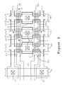
- FIG. 2 represents a top view of a conventional mode of implantation of six adjacent memory points on a silicon wafer.
- the various floating-gate transistors constituting the array of memory points are designated by Tij, where i is a row index and j a column index.
- the transistors T11 to T13 are those of the first row
- the transistors T21 to T23 are those of the second row.
- the transistors T11 and T21 are those of the first column
- the transistors T12 and T22 are those of the second column
- the transistors T13 and T23 are those of the third column.
- the control gates of the transistors of the same row are all connected to the same word line, LM1 and LM2 for the rows 1 and 2, respectively.
- the drains of the transistors of the same column are all connected to the same bit line, LB1 to LB3 for columns 1 to 3, respectively.
- the word lines are conductors (in practice in polycrystalline silicon) extending in a horizontal direction (direction of the rows).
- Bit lines are conductors extending in a vertical direction (direction of columns).
- bit lines pass over the transistors Tij forming the memory points.
- the floating gates 1 of the transistors are located between the drains 4 and the sources 3.
- the sources of the transistors of the same row are all connected to a common line L.
- All the common lines L are connected by a contact 12 to a conductive line A which, being itself at the source potential Vss, makes it possible to apply the voltage Vss to the sources of the transistors.
- An isolation zone 13 is located between each common line L and between each column of transistors.
- the isolation zone is made of thick silicon oxide (compared to the gate oxide).
- the floating gate 1 of the transistors overflows onto the isolation zone.
- FIG. 3 is a section along the axis YY ′ in FIG. 2.
- the floating grid 1 runs along the row of transistors and acts as a control grid 2 at the location of the transistors.
- the word line LM1 is covered by an insulating layer 14.
- This insulating layer 14 is for example made of silicon oxide doped with boron and phosphorus (BPSG) which makes it possible to obtain good creep at low temperatures (around 850 at 950 ° C).
- BPSG boron and phosphorus
- the bit lines LB2 and LB3 are located on the insulating layer 14, above the transistors T12 and T13 respectively.
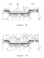
- Figure 4 shows a sectional view along the axis ZZ ′ of Figure 2, the two transistors T12 and T22.
- each transistor comprises a source region 3 and a drain region 4 separated by a channel region 7, as well as the superposition of the layers forming the gate oxide 5, the floating gate 1 , the interpoly oxide 6 and the control grid 2.
- the control gates of the transistors are covered by the insulating layer 14.
- the bit line LB2 is connected to the drains of the two transistors by the contact 11.
- bit line LB2 when it comes into contact with the drain regions of the transistors T12 and T22. All bit lines, made for example of aluminum, will be subjected to walking passages every two rows of transistors, which constitutes a significant risk of breaking of the aluminum lines.
- the present invention provides an architecture which avoids these drawbacks and has the advantage of having a high coupling factor.
- FIG. 5A represents the structure at an intermediate stage of manufacture after deposition of two levels of polycrystalline silicon.
- FIG. 5B represents the structure after deposition of a third level of polycrystalline silicon and etching of the various levels of polycrystalline silicon.
- the transistors are always arranged in an array of rows and columns, the transistors of the first row still being designated by T11 and T12, those of the second row by T21 and T22, and the transistor Tij more generally designating the transistor which is at the crossroads of row i and column j.
- the control gates of the transistors in row i are still all connected to a general direction conductor horizontal called word line LMi.
- the word lines are also conductors (in practice in polycrystalline silicon) extending in a horizontal direction (direction of the rows).
- the bit lines LBj consist of regions of the substrate of a first type of conductivity, for example n+. Each bit line acts directly as a drain 21 at the location of each transistor. There is therefore no longer any need to provide a contact every two rows of transistors on each of the bit lines (contacts designated by 11 in FIG. 2).
- Lines with constant potential, conductive, of general vertical direction, are inserted every second time between two bit lines, they are designated by B.
- These lines with constant potential B are constituted by regions of the first type of conductivity, such as bit lines LBj, and they act as sources 22 at the locations of the transistors.
- isolation zones 24 which are in principle made of thick silicon oxide.
- the floating gates 23 of the transistors are produced by a first level of polycrystalline silicon (poly 1) and located on each side of each line with constant potential B.
- Zones E produced by the first level of polycrystalline silicon, cover the edges adjacent to the columns of transistors of the isolation zones (24) and extend beyond it by a length 1.
- the floating gates 23 are still part, at the manufacturing stage represented in FIG. 5A, strips of poly 1 designated by P1 which extend in the direction of the columns.
- the strips of poly 1 P1 have been etched and the floating grids 23 are formed definitively by rectangles of poly 1.
- a layer 35 ′ produced by the second level of polycrystalline silicon (poly 2) is connected to each strip of poly 1 P1 extending in the direction of the columns.
- the layers 35 ′ have a greater width than that of the strips of poly 1 P1.
- zones 35 formed by the poly 2 are observed which are the remaining part of the layer 35 ′ after etching of the latter.
- Each zone 35 is connected to a floating grid 23.
- the dimensions along the direction of the columns of the zones 35 are identical to those of the floating grids 23, and the dimensions along the direction of the rows of the zones 35 are greater than those of the floating grids 23.
- the zones 35 extend beyond the floating grids 23, on the side of the source regions 22, of a length a, and the zones 35 pass over the zones E and extend beyond it by a length b.
- the word lines LM1 and LM2 are formed by a third level of polycrystalline silicon (poly 3).
- the current in the channel will flow in the horizontal direction, or direction of the word lines, and thus, the transistor will have a channel region oriented in the same direction. than the word lines.
- FIGS. 6A to 6G represent sectional views along the axis YY ′ of FIGS. 5A or 5B, they each correspond to a step in the process for manufacturing the structure according to the invention carried out in a silicon substrate 20.
- FIG. 6A represents the structure at a preliminary stage after completion of the thick oxide zones 24 and of the gate oxide layers 27, after deposition and etching of the first level of polycrystalline silicon to form on the one hand strips of poly 1 P1 in which the floating gates 23 of the transistors and on the other hand the zones E will be defined subsequently.
- the thick oxide zones 24 have for example a thickness of 700 nm and the gate oxide layers 27 have for example a thickness of 20 nm.
- P-type regions 18 are located under the thick oxide zones 24. These regions 18 are commonly called channel stop regions. Also shown are doped regions 19 located under the gate oxide layers 27 to define the triggering threshold of the transistors of the memory.
- FIG. 6B represents the structure at an intermediate stage after formation of heavily doped N + type regions which constitute on the one hand the bit lines LBj and on the other hand the lines with constant potential B. These regions are produced by implantation of arsenic.
- FIG. 6B also shows the structure after deposition of an insulation layer 36 between the different poly 1 zones. Conventionally, a planarization process is used so that the upper surfaces of this layer 36 and of the first silicon level polycrystalline are at the same level.
- This layer 36 consists of silicon oxide obtained for example by vapor deposition from a TEOS source (tetraethyl ortho silicate).
- FIG. 6C shows the structure at an intermediate stage after deposition of the second level of polycrystalline silicon 35 ′ and production of an insulating layer 28, which is commonly called an interpoly oxide layer, and which is formed in this structure by a stack of three layers silicon oxide / silicon nitride / silicon oxide called ONO.
- FIG. 6D represents the structure at an intermediate stage after etching of the interpoly oxide layer 28 and of the second level of polycrystalline silicon 35 ′ at the level of a part of the insulation layer 36 located at the location of the lines to constant potential B and on the other hand of the insulating layer 36 situated above the thick oxide zones 24.
- FIG. 6D also shows the structure after completion of an oxide zone 37, called the corner oxide zone, at each end, in the direction of the rows, of the layers 35 ′ defined by the etching.
- FIG. 6E represents the structure at an intermediate stage after deposition of the third level of polycrystalline silicon (poly 3) from which the word lines LMi are formed, and etching of the poly 3, of the ONO 28 interpoly oxide layer, of the poly 2 and poly 1 which makes it possible to define the word lines LMi formed in the poly 3, the zones 35 formed in the layers 35 ′, and the floating grids 23 formed in the strips of poly 1 P1.
- poly 3 the third level of polycrystalline silicon
- Figure 7 shows a sectional view along the axis ZZ ′ of Figure 5B.
- FIG. 6F represents the structure at an intermediate stage after deposition of an insulating layer 29.
- This layer 29 is for example made of silicon oxide doped with boron and phosphorus (BPSG).
- FIG. 6G represents the structure in the final step after production of conductive lines 30 situated on the insulating layer 29 and constituted for example of aluminum, each being placed above a bit line.
- bit lines of other memory blocks are connected to bit lines of other memory blocks (indeed, memory points are usually grouped into blocks occupying a certain number of rows and columns) thus making it possible to apply the desired potential to these bit lines and to the drains of the transistors to which the bit lines are connected.
- the conductive lines 30 extend over a flat surface, which makes it possible to avoid the problems due to the passage of step to which the aluminum lines are subjected in the classic configuration.
- the space existing between the pairs of conductive lines 30 is greater than the space existing between the pairs of aluminum lines constituting the bit lines in the conventional configuration.
- FIG. 7 which represents a sectional view along the axis ZZ ′ of FIG. 5B, we see the floating gates 23 of the transistors, these floating gates being located above the gate oxide layer 27. On also observes the zones 35 formed by the second level of polycrystalline silicon, and the ONO interpoly oxide layers 28 located above the zones 35. We also observe the two word lines LM1 and LM2 which act as control grids 25 at the location of the transistors.
- FIG. 8A represents a diagram of the capacities existing at the location of a transistor in the case where the architecture does not have a zone 35 connected to the floating gate 23 of the transistor
- FIG. 8B represents a diagram of the capacities existing at the location of a transistor in the case of the architecture according to the invention.
- V F ⁇ V M and which is defined by the ratio between the capacity at the interpoly oxide layer and the sum of all the capacities present.
- the numerical value of the coupling factor is then equal to the ratio between the quantities 0.8 / 20 and 0.8 / 20 + 0.8 / 20.
- the coupling factor is then equal to 0.5.
- a capacitance again appears at the level of the interpoly oxide layer 28 denoted C ′ OI and situated between the line of word LM2 and zone 35.
- C ′ OI a capacity at the level of the gate oxide layer 27 denoted C ′ OG .
- C OA a capacity corresponding to the zone portion 35 which extends beyond the floating grid 23 by a length a in the direction of the rows, a capacity C OD at the level of the oxide part of TEOS type.
- a capacity C BO corresponding to the part of the zone E which extends beyond a length 1 beyond the isolation zones 24, at the level of the part of the oxide layer grid 27 located between the part of zone E which projects and the substrate 20, a capacitance C ZI corresponding to the part of zone E situated above the isolation zone 24, at the level of this isolation zone 24, and a capacitance C OB corresponding to the overflow of the zone 35 beyond the zone E of a length b, at the level of the TEOS type oxide part separating two zones E and of the isolation zone 24.
- a numerical value representative of the coupling factor can be calculated using the following usual values: - overflow of zone 35 beyond the floating grid in the direction of the rows, designated by a: 0.2 micrometer - length of the floating grid in the direction of the rows: 0.8 micrometer - length of the TEOS type oxide part which separates the floating grid 23 from the zone E: 0.8 micrometer - overflow of zone E beyond isolation zone 24 in the direction of the rows: 0.4 micrometer - length of zone E in the direction of the rows: 0.8 micrometer - overflow of zone 35 beyond zone E in the direction of the rows, designated by b: 0.2 micrometer - thickness of the interpoly oxide layer: 20 nm - thickness of the gate oxide layer: 20 nm - thickness of the TEOS type oxide: 200 nm - thickness of the isolation zone: 700 nm
- the numerical value of the coupling factor is then equal to the ratio between the quantities (0.2 + 0.8 + 0.8 + 0.8 + 0.2) / 20 and (0.2 + 0.8 + 0, 8 + 0.8 + 0.2) / 20 + 0.2 / (200 + 20) + 0.8 / 20 + 0.8 / (200 + 20) + 0.4 / 20 + 0.4 / 700 + 0.2 / (200 + 700).
- the coupling factor is then substantially equal to 0.70.
- This architecture by the presence of the zone 35 connected to the floating gate 23 of the transistor, thus makes it possible to obtain a significantly improved coupling factor.
- FIG. 9 represents a variant of the invention.
- This figure which is a sectional view similar to the view shown in FIG. 6G, shows the various elements constituting the architecture according to the invention, the main ones being: - A floating gate 23, produced by a first level of polycrystalline silicon, at the location of each transistor; - two bit lines LB1 and LB2, which act as drain 21 at the location of the transistors; - two isolation zones 24, made of thick silicon oxide; a word line LM1, produced by a third level of polycrystalline silicon, which acts as a control grid 25 at the location of the transistors; - A line with constant potential, which is designated here by B ′, and which however has a structure different from that shown in FIG. 6G.
- the gate oxide layer which is designated in FIG. 9 by 27 ′, is very thin compared to the usual values, it has for example a thickness of the around 10 nm.
- the constant potential line B ′ consists of two parts doped to a different degree. There is a first heavily doped part 22-1, the doping being for example N+; this first part is located in a box 22-2 of the same type of conductivity with low doping, the doping then being for example N ⁇ .
- the constant potential line B ′ still acts as a source 22 ′ at the location of the transistors.
- This new arrangement allows, if a sufficiently high voltage is applied to the source 22 ′, the transfer by tunnel effect of charge carriers, trapped during a programming operation in the floating gate of the transistors, from the floating gate to the part from the high doping source. This transfer is made possible by the great thinness of the gate oxide layer, it is represented by the arrow in FIG. 9.
- the presence of the second lightly doped part makes it possible to increase the breakdown voltage between the source and the substrate.
- the advantage presented by the architecture according to the invention lies in the fact that the regions of thin oxide through which the charge carriers pass are never in contact with or near a zone of thick oxide.
Abstract
Description
La présente invention concerne les mémoires à semiconducteur, et plus particulièrement les mémoires non-volatiles électriquement programmables, plus couramment appelées mémoires EPROM ; la fabrication des mémoires à grille flottante est plus précisément concernée.The present invention relates to semiconductor memories, and more particularly to electrically programmable non-volatile memories, more commonly called EPROM memories; the manufacture of floating gate memories is more specifically concerned.
Pour obtenir des mémoires de grande capacité de stockage, par exemple des mémoires capables de stocker jusqu'à 16 mégabits, on doit réduire le plus possible la dimension de chacune des cellules constituant la mémoire.To obtain memories with large storage capacity, for example memories capable of storing up to 16 megabits, the size of each of the cells constituting the memory must be reduced as much as possible.
Mais on est évidemment limité par des considérations physiques, et notamment par la finesse des motifs que permettent les étapes de photolithographie ; on est limité aussi par les paramètres électriques parasites qui sont dus au processus de fabrication et qui perturbent le fonctionnement de la mémoire.However, it is obviously limited by physical considerations, and in particular by the fineness of the patterns which the photolithography stages allow; one is also limited by the parasitic electrical parameters which are due to the manufacturing process and which disturb the functioning of the memory.
Sauf quelques exceptions qui n'ont pas encore eu de succès industriel, toutes les approches essayées pour conduire à des mémoires de grande capacité correspondent à une technologie dont les points essentiels sont les suivants :
- le point-mémoire individuel est constitué d'un transistor ayant une grille flottante réalisée par un premier niveau de silicium polycristallin et une grille de commande réalisée par un deuxième niveau de silicium polycristallin ;
- les sources des transistors sont connectées à un bus à potentiel bas Vss ;
- la ligne de mot pour désigner une ligne de cellules est constituée du deuxième niveau de silicium polycristallin ;
- la ligne de bit pour lire l'état d'une cellule est constituée d'une ligne de métal (aluminium) croisant les lignes de mot et contactant de place en place le drain des transistors ;
- pour réduire la taille du point-mémoire, on prévoit qu'un seul point de contact est prévu pour deux drains adjacents de deux transistors d'une même colonne, ce contact assurant la connexion à la ligne de bit ; de même, on prévoit un seul contact entre les sources de deux transistors adjacents et le bus à Vss ;
- les transistors sont séparés les uns des autres par de l'oxyde de silicium épais (comparativement à l'oxyde de grille des transistors), et les lignes de bit et les lignes de mot passent au-dessus de cet oxyde épais ;
- enfin, l'écriture d'une information dans une cellule de la mémoire se fait de la manière suivante : les sources de tous les transistors de la mémoire sont à un potentiel bas Vss (par exemple zéro voit) ; la ligne de mot connectée à la grille de commande de la cellule à programmer est portée à un potentiel de programmation Vpp (par exemple 15 volts), tandis que toutes les autres lignes de mot sont au potentiel bas Vss ; la ligne de bit correspondant au point à programmer est portée à un potentiel haut Vcc (par exemple 10 volts), tandis que les lignes de bit des points qui ne doivent pas être programmés sont maintenues au potentiel bas Vss.With a few exceptions which have not yet had industrial success, all the approaches tried to lead to high-capacity memories correspond to a technology whose essential points are the following:
- The individual memory point consists of a transistor having a floating gate produced by a first level of polycrystalline silicon and a control gate produced by a second level of polycrystalline silicon;
- the sources of the transistors are connected to a low potential bus Vss;
- the word line to designate a line of cells consists of the second level of polycrystalline silicon;
- the bit line for reading the state of a cell consists of a metal (aluminum) line crossing the word lines and contacting from place to place the drain of the transistors;
- To reduce the size of the memory point, it is provided that a single contact point is provided for two adjacent drains of two transistors of the same column, this contact ensuring the connection to the bit line; similarly, a single contact is provided between the sources of two adjacent transistors and the bus at Vss;
- the transistors are separated from each other by thick silicon oxide (compared to the gate oxide of the transistors), and the bit lines and the word lines pass over this thick oxide;
- finally, the writing of information in a memory cell is done as follows: the sources of all the transistors of the memory are at a low potential Vss (for example zero sees); the word line connected to the control grid of the cell to be programmed is brought to a programming potential Vpp (for example 15 volts), while all the other word lines are at low potential Vss; the bit line corresponding to the point to be programmed is brought to a high potential Vcc (for example 10 volts), while the bit lines of the points which should not be programmed are kept at the low potential Vss.
Avec cette architecture de mémoire et le mode de programmation associé, il est impératif que le drain d'un transistor soit électriquement isolé, par de l'oxyde épais, du drain des transistors adjacents de la même ligne de mot, faute de quoi on ne pourrait programmer un point-mémoire particulier sans programmer ou déprogrammer en même temps les autres.With this memory architecture and the associated programming mode, it is imperative that the drain of a transistor be electrically isolated, by thick oxide, from the drain of adjacent transistors of the same word line, otherwise we will not could program a particular memory point without programming or deprogramming the others at the same time.
Mais l'oxyde épais qui isole deux points adjacents occupe beaucoup de place, surtout lorsqu'il est réalisé par la technique dite d'oxydation localisée.However, the thick oxide which isolates two adjacent points takes up a lot of space, especially when it is produced by the so-called localized oxidation technique.
On a essayé de remplacer l'oxydation localisée par une isolation par tranchées remplies d'oxyde, pour réduire l'encombrement global de la cellule, mais cette technologie n'est pas industriellement au point.Attempts have been made to replace localized oxidation with insulation by trenches filled with oxide, in order to reduce the overall bulk of the cell, but this technology is not industrially developed.
On a également proposé (demande de brevet français 86/12938) des structures où les zones d'oxyde épais et les contacts multiples vers les drains ou sources sont supprimés. Ces structures permettent effectivement une miniaturisation du réseau mémoire mais au prix d'une complexification du système d'adressage et donc d'une augmentation de la surface occupée par celui-ci.We have also proposed (French patent application 86/12938) structures where the thick oxide zones and the multiple contacts to the drains or sources are eliminated. These structures effectively allow a miniaturization of the memory network but at the cost of a complexification of the addressing system and therefore of an increase in the surface occupied by it.
Pour réduire l'encombrement des cellules et ainsi augmenter la capacité de stockage de la mémoire, la présente invention propose une nouvelle architecture de mémoire qui permet de ne prévoir une telle zone d'oxyde épais que tous les deux transistors connectés à une même ligne de mot. De plus, la nouvelle architecture proposée permet d'éviter la présence de contacts sur les lignes de bit entre les cellules.To reduce the size of the cells and thus increase the storage capacity of the memory, the present invention proposes a new memory architecture which makes it possible to provide such a thick oxide zone only for both transistors connected to the same line of word. In addition, the new architecture proposed makes it possible to avoid the presence of contacts on the bit lines between the cells.
Selon l'invention, la mémoire est composée d'un réseau de lignes de mot s'étendant suivant une première direction, dite de rangée, reliant des grilles de commande de transistors à grille flottante, et de lignes de bit s'étendant suivant une deuxième direction, dite de colonne, reliant des drains des transistors à grille flottante. Une zone conductrice, de dimensions supérieures à celles de la grille flottante des transistors suivant un plan horizontal, est reliée à la grille flottante de chaque transistor de la mémoire, tout en étant située en regard de la ligne de mot correspondante dont elle est séparée par une couche d'isolement.According to the invention, the memory is composed of a network of word lines extending in a first direction, called a row direction, connecting control gates of floating-gate transistors, and bit lines extending in a second direction, called column direction, connecting drains of floating gate transistors. A conductive area, of dimensions greater than those of the floating gate of the transistors in a horizontal plane, is connected to the floating gate of each transistor of the memory, while being situated opposite the corresponding word line from which it is separated by an isolation layer.
Selon un autre aspect de la présente invention, il est prévu un procédé de fabrication de mémoire, de type MOS à transistors à grille flottante disposés selon des rangées et des colonnes sur un substrat d'un premier type de conductivité, comprenant les étapes suivantes :
- réaliser des zones d'oxyde épais selon des colonnes,
- déposer et graver un premier niveau de silicium polycristallin pour former selon des colonnes d'une part deux premières bandes adjacentes entre chaque paire de colonnes d'oxyde épais, d'autre part deux deuxièmes bandes dont chacune est à cheval entre la partie comprise à l'intérieur de cette paire et une partie de la zone d'oxyde épais correspondante,
- réaliser une implantation du deuxième type de conductivité en utilisant le premier niveau de silicium polycristallin comme masque,
- former une couche d'isolement entre les différentes zones de premier niveau de silicium polycristallin,
- déposer un deuxième niveau de silicium polycristallin et l'isoler superficiellement,
- graver le deuxième niveau de silicium polycristallin (35) pour qu'il recouvre selon des colonnes des première et deuxième bandes adjacentes du premier niveau de silicium polycristallin,
- isoler latéralement les régions apparentes du deuxième niveau de silicium polycristallin,
- déposer un troisième niveau de silicium polycristallin,
- graver par un même masque, selon des rangées, les trois niveaux de silicium polycristallin,
- former une couche isolante, et
- établir des contacts avec les bandes restantes du troisième niveau de silicium polycristallin (lignes de mot), les colonnes de drains (lignes de bit), et les colonnes de sources (lignes à potentiel constant).According to another aspect of the present invention, there is provided a memory manufacturing method, of the MOS type with floating gate transistors arranged in rows and columns on a substrate of a first type of conductivity, comprising the following steps:
- make thick oxide zones according to columns,
deposit and etch a first level of polycrystalline silicon to form, according to columns, on the one hand, two adjacent first bands between each pair of thick oxide columns, and on the other hand, two second bands, each of which straddles the part included the inside of this pair and part of the corresponding thick oxide area,
- carry out an implantation of the second type of conductivity using the first level of polycrystalline silicon as a mask,
- forming an isolation layer between the different first level areas of polycrystalline silicon,
- deposit a second level of polycrystalline silicon and isolate it superficially,
- etching the second level of polycrystalline silicon (35) so that it covers, in columns, the first and second adjacent strips of the first level of polycrystalline silicon,
- laterally isolate the visible regions of the second level of polycrystalline silicon,
- deposit a third level of polycrystalline silicon,
- engrave with the same mask, in rows, the three levels of polycrystalline silicon,
- form an insulating layer, and
- establish contacts with the remaining bands of the third level of polycrystalline silicon (word lines), the columns of drains (bit lines), and the columns of sources (lines with constant potential).
Ces objets, caractéristiques et avantages ainsi que d'autres de la présente invention seront exposés plus en détail dans la description suivante d'un mode de réalisation particulier faite en relation avec les figures jointes parmi lesquelles :
- les figures 1A et 1B représentent une cellule élémentaire de mémoire classique, la figure 1A étant une représentation sous forme de schéma électrique et la figure 1B étant une vue en coupe schématique de la cellule élémentaire ;
- la figure 2 représente une vue de dessus de l'implantation de six points mémoires adjacents sur une tranche de silicium selon l'art antérieur ;
- la figure 3 représente une vue en coupe suivant l'axe YY′ de la figure 2 ;
- la figure 4 représente une vue en coupe suivant l'axe ZZ′ de la figure 2 ;
- les figures 5A et 5B représentent chacune une vue de dessus de l'implantation de quatre points-mémoire adjacents sur une tranche de silicium selon la présente invention, à deux étapes de fabrication différentes ;
- les figures 6A à 6G représentent les différentes étapes du procédé de fabrication selon l'invention ;
- la figure 7 représente une vue en coupe suivant l'axe ZZ′ de la figure 5B ;
- les figures 8A et 8B représentent chacune un schéma des capacités existant à l'emplacement d'un transistor, suivant deux modes de réalisation différents ; et
- la figure 9 représente une variante de réalisation de l'invention.
- FIGS. 1A and 1B represent an elementary cell of conventional memory, FIG. 1A being a representation in the form of an electrical diagram and FIG. 1B being a schematic sectional view of the elementary cell;
- FIG. 2 represents a top view of the implantation of six adjacent memory points on a silicon wafer according to the prior art;
- 3 shows a sectional view along the axis YY ′ of Figure 2;
- 4 shows a sectional view along the axis ZZ 'of Figure 2;
- FIGS. 5A and 5B each represent a top view of the layout of four adjacent memory points on a silicon wafer according to the present invention, in two different manufacturing stages;
- FIGS. 6A to 6G represent the different stages of the manufacturing process according to the invention;
- 7 shows a sectional view along the axis ZZ 'of Figure 5B;
- FIGS. 8A and 8B each represent a diagram of the capacities existing at the location of a transistor, according to two different embodiments; and
- FIG. 9 represents an alternative embodiment of the invention.
De façon générale, comme cela est classique dans la représentation des circuits intégrés, on notera que les diverses figures ne sont pas représentées à l'échelle ni d'une figure à l'autre, ni à l'intérieur d'une même figure, et notamment que les épaisseurs des couches sont dessinées arbitrairement dans le but de faciliter la lecture des figures.In general, as is conventional in the representation of integrated circuits, it will be noted that the various figures are not represented to scale, neither from one figure to another, nor inside the same figure, and in particular that the thicknesses of the layers are drawn arbitrarily in order to facilitate the reading of the figures.
La figure 1A représente un transistor T d'un point-mémoire à grille flottante. Ce transistor possède une grille flottante 1 et une grille de commande 2, ainsi que deux régions semiconductrices d'un premier type de conductivité (source 3 et drain 4) séparées par une région de canal d'un type de conductivité opposé recouverte par la grille flottante 1 et la grille de commande 2.FIG. 1A represents a transistor T of a floating gate memory point. This transistor has a
La grille de commande 2 est reliée à une ligne de mot LM. Le drain 4 est relie à une ligne de bit LB.The
Pour programmer, ou écrire, un tel point-mémoire, on charge sa grille flottante 1 par injection de porteurs chauds, en appliquant à la grille de commande 2, pendant que le transistor conduit un courant entre ses régions de source 3, mises à la masse, et de drain 4, un potentiel suffisamment élevé pour que les porteurs de charge (électrons) soient attirés et piégés dans la grille flottante. Cette opération d'écriture a pour effet d'augmenter le seuil de conduction du transistor qui, une fois programmé, ne conduira le courant que pour des valeurs de potentiel appliqué sur la grille de commande plus élevées qu'en l'absence de programmation.To program, or write, such a memory point, its
Lors de la lecture de l'information contenue dans un point-mémoire, on applique à la grille de commande du transistor de ce point-mémoire une tension à la fois supérieure à la tension de seuil de déclenchement de conduction à l'état non-programmé et inférieure à la tension de seuil de déclenchement de conduction à l'état programmé. Si le transistor conduit le courant quand une différence de potentiel adaptée est appliquée entre la source et le drain, le point-mémoire est à l'état non-programmé. Si le transistor ne conduit pas le courant, le point-mémoire est à l'état programmé.When reading the information contained in a memory point, a voltage is applied to the control gate of the transistor of this memory point that is both greater than the conduction trigger threshold voltage in the non-state programmed and lower than the conduction trigger threshold voltage in the programmed state. If the transistor conducts current when a suitable potential difference is applied between the source and the drain, the memory point is in the non-programmed state. If the transistor does not conduct current, the memory point is in the programmed state.
Le potentiel appliqué à la grille de commande lorsqu'on programme le point-mémoire, ou potentiel de programmation Vpp, est par exemple de 15 volts. Le potentiel de drain Vcc est alors par exemple de 10 volts, et le potentiel de source Vss est par exemple zéro volt, ou la masse.The potential applied to the control grid when programming the memory point, or Vpp programming potential, is for example 15 volts. The drain potential Vcc is then by example of 10 volts, and the source potential Vss is for example zero volts, or ground.
Le potentiel appliqué à la grille de commande lors de la lecture du point-mémoire est par exemple de 5 volts. Le potentiel de drain Vcc est alors par exemple de 1,5 volts, et le potentiel e source Vss est par exemple zéro volt, ou la masse.The potential applied to the control grid when reading the memory point is for example 5 volts. The drain potential Vcc is then for example 1.5 volts, and the source potential Vss is for example zero volts, or ground.
Sur la figure 1B, qui représente une vue en coupe d'un point-mémoire implanté sur une tranche de silicium, on retrouve la grille flottante 1 et la grille de commande 2 du transistor. On voit également la source 3 et le drain 4, qui sont deux régions semiconductrices d'un premier type de conductivité, par exemple N⁺, séparées par une région de canal 7 d'un type de conductivité opposé, par exemple P⁻.In FIG. 1B, which represents a sectional view of a memory point implanted on a silicon wafer, there is the floating
La grille flottante 1 du transistor est réalisée par un premier niveau de silicium polycristallin (poly 1). Elle est séparée du substrat par une couche de dioxyde de silicium 5, également appelée couche d'oxyde de grille.The floating
Au-dessus de la grille flottante 1, on trouve une couche de dioxyde de silicium 6. Cette couche est située entre la grille flottante 1 et la grille de commande 2, cette dernière étant réalisée par un deuxième niveau de silicium polycristallin (poly 2). La couche de dioxyde de silicium 6 porte ainsi également le nom de couche d'oxyde interpoly.Above the floating
Dans la mémoire, la grille de commande 2 du transistor est reliée à une ligne de mot LM. La source 3 est reliée à la masse, et le drain 4 à une ligne de bit LB.In memory, the
La figure 2 représente en vue de dessus un mode d'implantation classique de six points-mémoire adjacents sur une tranche de silicium.FIG. 2 represents a top view of a conventional mode of implantation of six adjacent memory points on a silicon wafer.
On désigne par Tij les différents transistors à grille flottante constituant le réseau de points-mémoire, où i est un indice de rangée et j un indice de colonne.The various floating-gate transistors constituting the array of memory points are designated by Tij, where i is a row index and j a column index.
Ainsi, les transistors T11 à T13 sont ceux de la première rangée, les transistors T21 à T23 sont ceux de la deuxième rangée.Thus, the transistors T11 to T13 are those of the first row, the transistors T21 to T23 are those of the second row.
De même, les transistors T11 et T21 sont ceux de la première colonne, les transistors T12 et T22 sont ceux de la deuxième colonne et enfin les transistors T13 et T23 sont ceux de la troisième colonne.Likewise, the transistors T11 and T21 are those of the first column, the transistors T12 and T22 are those of the second column and finally the transistors T13 and T23 are those of the third column.
Les grilles de commande des transistors d'une même rangée sont toutes reliées à une même ligne de mot, LM1 et LM2 pour les rangées 1 et 2, respectivement.The control gates of the transistors of the same row are all connected to the same word line, LM1 and LM2 for the
Les drains des transistors d'une même colonne sont tous reliés à une même ligne de bit, LB1 à LB3 pour les colonnes 1 à 3, respectivement.The drains of the transistors of the same column are all connected to the same bit line, LB1 to LB3 for
Les lignes de mot sont des conducteurs (en pratique en silicium polycristallin) s'étendant selon une direction horizontale (direction des rangées). Les lignes de bit sont des conducteurs s'étendant dans une direction verticale (direction des colonnes).The word lines are conductors (in practice in polycrystalline silicon) extending in a horizontal direction (direction of the rows). Bit lines are conductors extending in a vertical direction (direction of columns).
Les lignes de bit passent au-dessus des transistors Tij formant les points-mémoire.The bit lines pass over the transistors Tij forming the memory points.
Elles sont reliées aux drains 4 des transistors par des contacts 11. Les grilles flottantes 1 des transistors sont situées entre les drains 4 et les sources 3.They are connected to the
Les sources des transistors d'une même rangée sont toutes reliées à une ligne commune L. couple de deux rangées de transistors, séparé d'un couple adjacent par une rangée de contacts 11, partage une ligne commune L unique, qui est placée entre les deux rangées.The sources of the transistors of the same row are all connected to a common line L. couple of two rows of transistors, separated from an adjacent couple by a row of
Toutes les lignes communes L sont reliées par un contact 12 à une ligne conductrice A qui, étant elle-même au potentiel de source Vss, permet d'appliquer aux sources des transistors la tension Vss.All the common lines L are connected by a
Une zone d'isolement 13 est située entre chaque ligne commune L et entre chaque colonne de transistors. En pratique, la zone d'isolement est réalisée en oxyde de silicium épais (comparativement à l'oxyde de grille).An
La grille flottante 1 des transistors déborde sur la zone d'isolement.The floating
Deux transistors, par exemple les transistors T12 et T13, sont représentés sur la figure 3 qui est une coupe suivant l'axe YY′ de la figure 2.Two transistors, for example the transistors T12 and T13, are shown in FIG. 3 which is a section along the axis YY ′ in FIG. 2.
Ils sont séparés par une zone d'isolement 13. Sous la grille flottante 1 se trouve la couche d'oxyde de grille 5. La grille flottante 1 a des dimensions plus grandes suivant cette direction de coupe que la couche d'oxyde de grille 5, et elle déborde sur les zones d'isolement. On observe au-dessus de la grille flottante la couche d'oxyde interpoly 6. La ligne de mot LM1 court le long de la rangée de transistors et fait office de grille de commande 2 à l'emplacement des transistors.They are separated by an
La ligne de mot LM1 est recouverte par une couche isolante 14. Cette couche isolante 14 est par exemple réalisée en oxyde de silicium dopé au bore et au phosphore (BPSG) qui permet d'obtenir un bon fluage à faibles températures (d'environ 850 à 950°C).The word line LM1 is covered by an insulating
Les lignes de bit LB2 et LB3 sont situées sur la couche isolante 14, au-dessus des transistors T12 et T13 respectivement.The bit lines LB2 and LB3 are located on the insulating
On voit sur la figure 4, qui représente une vue en coupe suivant l'axe ZZ′ de la figure 2, les deux transistors T12 et T22.We see in Figure 4, which shows a sectional view along the axis ZZ ′ of Figure 2, the two transistors T12 and T22.
Comme cela a été montré sur la figure 1B, chaque transistor comprend une région de source 3 et une région de drain 4 séparées par une région de canal 7, ainsi que la superposition des couches formant l'oxyde de grille 5, la grille flottante 1, l'oxyde interpoly 6 et la grille de commande 2.As shown in FIG. 1B, each transistor comprises a
Les grilles de commande des transistors sont recouvertes par la couche isolante 14. La ligne de bit LB2 est reliée aux drains des deux transistors par le contact 11.The control gates of the transistors are covered by the insulating
L'architecture classique, telle qu'on vient de la décrire, présente cependant des éléments qui limitent la réduction des dimensions. D'une part, on trouve une série de contacts entre lignes de bit et régions de drains toutes les deux rangées de transistors. D'autre part, on voit sur la figure 2 qu'une zone d'isolement 13, réalisée en oxyde de silicium épais, est située entre chaque paire de lignes communes 2 et entre chaque paire de colonnes de transistors.Classical architecture, as we have just described it, however presents elements which limit the reduction of dimensions. On the one hand, there are a series of contacts between bit lines and drain regions every two rows of transistors. On the other hand, it can be seen in FIG. 2 that an
Egalement, on voit sur la figure 4 un passage de marche de la ligne de bit LB2 lors de sa prise de contact avec les régions de drains des transistors T12 et T22. Toutes les lignes de bit, réalisées par exemple en aluminium, vont être soumises à des passages de marche toutes les deux rangées de transistors, ce qui constitue un risque important de cassure des lignes d'aluminium.Also, we see in Figure 4 a walking passage of the bit line LB2 when it comes into contact with the drain regions of the transistors T12 and T22. All bit lines, made for example of aluminum, will be subjected to walking passages every two rows of transistors, which constitutes a significant risk of breaking of the aluminum lines.
La présente invention propose une architecture qui évite ces inconvénients et a l'avantage de présenter un facteur de couplage élevé.The present invention provides an architecture which avoids these drawbacks and has the advantage of having a high coupling factor.
Cette architecture est représentée en vue de dessus aux figures 5A et 5B. La figure 5A représente la structure à un stade intermédiaire de fabrication après dépôt de deux niveaux de silicium polycristallin. La figure 5B représente la structure après dépôt d'un troisième niveau de silicium polycristallin et gravure des divers niveaux de silicium polycristallin. Les transistors sont toujours disposés en réseau de rangées et colonnes, les transistors de la première rangée étant encore désignés par T11 et T12, ceux de la deuxième rangée par T21 et T22, et le transistor Tij désignant plus généralement le transistor qui est au carrefour de la rangée i et de la colonne j.This architecture is shown in top view in FIGS. 5A and 5B. FIG. 5A represents the structure at an intermediate stage of manufacture after deposition of two levels of polycrystalline silicon. FIG. 5B represents the structure after deposition of a third level of polycrystalline silicon and etching of the various levels of polycrystalline silicon. The transistors are always arranged in an array of rows and columns, the transistors of the first row still being designated by T11 and T12, those of the second row by T21 and T22, and the transistor Tij more generally designating the transistor which is at the crossroads of row i and column j.
Les grilles de commande des transistors de la rangée i sont encore toutes reliées à un conducteur de direction générale horizontale appelé ligne de mot LMi. Les lignes de mot sont encore des conducteurs (en pratique en silicium polycristallin) s'étendant selon une direction horizontale (direction des rangées).The control gates of the transistors in row i are still all connected to a general direction conductor horizontal called word line LMi. The word lines are also conductors (in practice in polycrystalline silicon) extending in a horizontal direction (direction of the rows).
Les lignes de bit LBj sont constituées de régions du substrat d'un premier type de conductivité, par exemple n⁺. Chaque ligne de bit fait directement office de drain 21 à l'emplacement de chaque transistor. Il n'y a donc plus besoin de prévoir un contact toutes les deux rangées de transistors sur chacune des lignes de bit (contacts désignés par 11 sur la figure 2).The bit lines LBj consist of regions of the substrate of a first type of conductivity, for example n⁺. Each bit line acts directly as a
Des lignes à potentiel constant, conductrices, de direction générale verticale, sont intercalées une fois sur deux entre deux lignes de bit, elles sont désignées par B. Ces lignes à potentiel constant B sont constituées par des régions du premier type de conductivité, comme les lignes de bit LBj, et elles font office de sources 22 aux emplacements des transistors.Lines with constant potential, conductive, of general vertical direction, are inserted every second time between two bit lines, they are designated by B. These lines with constant potential B are constituted by regions of the first type of conductivity, such as bit lines LBj, and they act as
De chaque côté des deux lignes de bit LB1 et LB2, représentées sur les figures 5A et 5B, qui sont situées de part et d'autre de la même ligne à potentiel constant B, se trouvent des zones d'isolement 24, qui sont en principe réalisée en oxyde de silicium épais.On each side of the two bit lines LB1 and LB2, shown in FIGS. 5A and 5B, which are located on either side of the same line with constant potential B, there are
Les grilles flottantes 23 des transistors sont réalisées par un premier niveau de silicium polycristallin (poly 1) et situées de chaque côté de chaque ligne à potentiel constant B.The floating
Des zones E, réalisées par le premier niveau de silicium polycristallin, recouvrent les bords adjacents aux colonnes de transistors des zones d'isolement (24) et en débordent d'une longueur 1. Les grilles flottantes 23 font encore partie, au stade de fabrication représenté à la figure 5A, de bandes de poly 1 désignées par P1 qui s'étendent suivant la direction des colonnes. Au stade de la fabrication présenté à la figure 5B, les bandes de poly 1 P1 ont été gravées et les grilles flottantes 23 sont formées de façon définitive par des rectangles de poly 1.Zones E, produced by the first level of polycrystalline silicon, cover the edges adjacent to the columns of transistors of the isolation zones (24) and extend beyond it by a
Sur la figure 5A, une couche 35′ réalisée par le deuxième niveau de silicium polycristallin (poly 2) est reliée à chaque bande de poly 1 P1 en s'étendant suivant la direction des colonnes. Les couches 35′ ont une largeur plus importante que celle des bandes de poly 1 P1. Sur la figure 5B, on observe des zones 35 constituées par le poly 2 qui sont la partie restante de la couche 35′ après gravure de celle-ci. Chaque zone 35 est reliée à une grille flottante 23. Les dimensions suivant la direction des colonnes des zones 35 sont identiques à celles des grilles flottantes 23, et les dimensions suivant la direction des rangées des zones 35 sont supérieures à celles des grilles flottantes 23. Suivant la direction des rangées, les zones 35 débordent des grilles flottantes 23, du côté des régions de sources 22, d'une longueur a, et les zones 35 passent au-dessus des zones E et en débordent d'une longueur b.In FIG. 5A, a
Les lignes de mot LM1 et LM2 sont constituées par un troisième niveau de silicium polycristallin (poly 3).The word lines LM1 and LM2 are formed by a third level of polycrystalline silicon (poly 3).
Puisque la source et le drain d'un transistor sont disposés selon une direction horizontale, le courant dans le canal circulera dans la direction horizontale, ou direction des lignes de mot, et ainsi, le transistor possèdera une région de canal orientée dans le même sens que les lignes de mot.Since the source and drain of a transistor are arranged in a horizontal direction, the current in the channel will flow in the horizontal direction, or direction of the word lines, and thus, the transistor will have a channel region oriented in the same direction. than the word lines.
Les figures 6A à 6G représentent des vues en coupe suivant l'axe YY′ des figures 5A ou 5B, elles correspondent chacune à une étape du procédé de fabrication de la structure selon l'invention réalisée dans un substrat de silicium 20.FIGS. 6A to 6G represent sectional views along the axis YY ′ of FIGS. 5A or 5B, they each correspond to a step in the process for manufacturing the structure according to the invention carried out in a
La figure 6A représente la structure à une étape préliminaire après réalisation des zones d'oxyde épais 24 et des couches d'oxyde de grille 27, après dépôt et gravure du premier niveau de silicium polycristallin pour former d'une part des bandes de poly 1 P1 dans lesquelles seront définies ultérieurement les grilles flottantes 23 des transistors et d'autre part les zones E. Les zones d'oxyde épais 24 ont par exemple une épaisseur de 700 nm et les couches d'oxyde de grille 27 ont par exemple une épaisseur de 20 nm. De façon classique, des régions 18 de type P sont situées sous les zones d'oxyde épais 24. Ces régions 18 sont couramment appelées régions d'arrêt de canal. On a également représenté des régions dopées 19 situées sous les couches d'oxyde de grille 27 pour définir le seuil de déclenchement des transistors de la mémoire.FIG. 6A represents the structure at a preliminary stage after completion of the
Pour une plus grande clarté des dessins, les régions 18 et 19 ne seront pas représentées sur les figures 6B à 6G.For greater clarity of the drawings, the
La figure 6B représente la structure à une étape intermédiaire après formation de régions de type N+ fortement dopées qui constituent d'une part les lignes de bit LBj et d'autre part les lignes à potentiel constant B. Ces régions sont réalisées par implantation d'arsenic.FIG. 6B represents the structure at an intermediate stage after formation of heavily doped N + type regions which constitute on the one hand the bit lines LBj and on the other hand the lines with constant potential B. These regions are produced by implantation of arsenic.
La figure 6B représente également la structure après dépôt d'une couche d'isolement 36 entre les différentes zones de poly 1. De façon classique, un procédé de planarisation est utilisé pour que les surfaces supérieures de cette couche 36 et du premier niveau de silicium polycristallin soient au même niveau. Cette couche 36 est constituée d'oxyde de silicium obtenu par exemple par dépôt en phase vapeur à partir d'une source TEOS (tétraéthyle ortho silicate).FIG. 6B also shows the structure after deposition of an
La figure 6C représente la structure à une étape intermédiaire après dépôt du deuxième niveau de silicium polycristallin 35′ et réalisation d'une couche d'isolant 28, que l'on appelle couramment couche d'oxyde interpoly, et qui est constituée dans cette structure par un empilement de trois couches oxyde de silicium/nitrure de silicium/oxyde de silicium appelé ONO.FIG. 6C shows the structure at an intermediate stage after deposition of the second level of
La figure 6D représente la structure à une étape intermédiaire après gravure de la couche d'oxyde interpoly 28 et du deuxième niveau de silicium polycristallin 35′ au niveau d'une part de la couche d'isolement 36 située à l'emplacement des lignes à potentiel constant B et d'autre part de la couche d'isolement 36 située au-dessus des zones d'oxyde épais 24.FIG. 6D represents the structure at an intermediate stage after etching of the
La figure 6D représente également la structure après réalisation d'une zone d'oxyde 37, appelée zone d'oxyde de coin, à chaque extrémité, suivant la direction des rangées, des couches 35′ définies par la gravure.FIG. 6D also shows the structure after completion of an
La figure 6E représente la structure à une étape intermédiaire après dépôt du troisième niveau de silicium polycristallin (poly 3) à partir duquel sont formées les lignes de mot LMi, et gravure du poly 3, de la couche d'oxyde interpoly ONO 28, du poly 2 et poly 1 qui permet de définir les lignes de mot LMi formées dans le poly 3, les zones 35 formées dans les couches 35′, et les grilles flottantes 23 formées dans les bandes de poly 1 P1.FIG. 6E represents the structure at an intermediate stage after deposition of the third level of polycrystalline silicon (poly 3) from which the word lines LMi are formed, and etching of the
La structure obtenue après la gravure de ces différentes couches peut également être observée sur la figure 7, qui représente une vue en coupe suivant l'axe ZZ′ de la figure 5B.The structure obtained after the etching of these different layers can also be observed in Figure 7, which shows a sectional view along the axis ZZ ′ of Figure 5B.
Il apparaît de plus sur la figure 6E que la couche d'oxyde interpoly ONO 28 et les zones d'oxyde de coin 37 assurent l'isolation entre les lignes de mot et les zones 35.It also appears in FIG. 6E that the ONO
La figure 6F représente la structure à une étape intermédiaire après dépôt d'une couche isolante 29. Cette couche 29 est par exemple réalisée en oxyde de silicium dopé au bore et au phosphore (BPSG).FIG. 6F represents the structure at an intermediate stage after deposition of an insulating
La figure 6G représente la structure à l'étape finale après réalisation de lignes conductrices 30 situées sur la couche isolante 29 et constituées par exemple en aluminium, chacune étant placée au-dessus d'une ligne de bit.FIG. 6G represents the structure in the final step after production of
Elles sont connectées à des lignes de bit d'autres blocs mémoire (en effet, les points-mémoire sont habituellement regroupés en blocs occupant un certain nombre de rangées et de colonnes) permettant ainsi d'appliquer le potentiel désiré à ces lignes de bit et aux drains des transistors auxquels les lignes de bit sont reliées.They are connected to bit lines of other memory blocks (indeed, memory points are usually grouped into blocks occupying a certain number of rows and columns) thus making it possible to apply the desired potential to these bit lines and to the drains of the transistors to which the bit lines are connected.
Les lignes conductrices 30 s'étendent sur une surface plane, ce qui permet d'éviter les problèmes dus aux passages de marche auxquels sont soumises les lignes d'aluminium dans la configuration classique.The
De plus, l'espace existant entre les paires de lignes conductrices 30 est supérieur à l'espace existant entre les paires de lignes d'aluminium constituant les lignes de bit dans la configuration classique.In addition, the space existing between the pairs of
Sur la figure 7, qui représente une vue en coupe suivant l'axe ZZ′ de la figure 5B, on voit les grilles flottantes 23 des transistors, ces grilles flottantes étant situées au-dessus de la couche d'oxyde de grille 27. On observe également les zones 35 formées par le deuxième niveau de silicium polycristallin, et les couches d'oxyde interpoly ONO 28 situées au-dessus des zones 35. On observe aussi les deux lignes de mot LM1 et LM2 qui font office de grilles de commande 25 à l'emplacement des transistors.In FIG. 7, which represents a sectional view along the axis ZZ ′ of FIG. 5B, we see the floating
La figure 8A représente un schéma des capacités existant à l'emplacement d'un transistor dans le cas où l'architecture ne présente pas de zone 35 reliée à la grille flottante 23 du transistor, et la figure 8B représente un schéma des capacités existant à l'emplacement d'un transistor dans le cas de l'architecture selon l'invention.FIG. 8A represents a diagram of the capacities existing at the location of a transistor in the case where the architecture does not have a
Dans les deux cas, si l'on applique une tension VM à la ligne de mot LM2, on obtient la tension VF sur la grille flottante en calculant le facteur de couplage γ qui relie ces deux tensions par la relation :
VF = γ VM
et qui est défini par le rapport entre la capacité au niveau de la couche d'oxyde interpoly et la somme de toutes les capacités présentes.In both cases, if a voltage V M is applied to the word line LM2, the voltage V F is obtained on the floating gate by calculating the coupling factor γ which connects these two voltages by the relation:
V F = γ V M
and which is defined by the ratio between the capacity at the interpoly oxide layer and the sum of all the capacities present.
Si l'on considère la figure 8A, on observe la capacité au niveau de la couche d'oxyde interpoly 28 notée COI et située entre la ligne de mot LM2 et la grille flottante 23. On a aussi une capacité COG au niveau de la couche d'oxyde de grille 27 située entre la grille flottante 23 et le substrat 20.If we consider FIG. 8A, we observe the capacitance at the level of the
Le facteur de couplage γ s'écrit :
γ = COI/(COI + COG).The coupling factor γ is written:
γ = C OI / (C OI + C OG ).
On peut calculer une valeur numérique représentative du facteur de couplage en utilisant des valeurs usuelles pour les dimensions des éléments concernés :
- longueur de la grille flottante suivant la direction des rangées : 0,8 micromètre.
- épaisseur de la couche d'oxyde interpoly : 20 nm
- épaisseur de la couche d'oxyde de grille : 20 nmOne can calculate a numerical value representative of the coupling factor by using usual values for the dimensions of the elements concerned:
- length of the floating grid in the direction of the rows: 0.8 micrometer.
- thickness of the interpoly oxide layer: 20 nm
- thickness of the gate oxide layer: 20 nm
La valeur numérique du facteur de couplage est alors égale au rapport entre les quantités 0,8/20 et 0,8/20 + 0,8/20. Le facteur de couplage est alors égal à 0,5.The numerical value of the coupling factor is then equal to the ratio between the quantities 0.8 / 20 and 0.8 / 20 + 0.8 / 20. The coupling factor is then equal to 0.5.
Si l'on considère la figure 8B, correspondant au cas où la zone 35 est reliée à la grille flottante du transistor, il apparaît de nouveau une capacité au niveau de la couche d'oxyde interpoly 28 notée C′OI et située entre la ligne de mot LM2 et la zone 35. On a aussi de nouveau une capacité au niveau de la couche d'oxyde de grille 27 notée C′OG. Il existe également une capacité COA correspondant à la partie de zone 35 qui déborde au-delà de la grille flottante 23 d'une longueur a suivant la direction des rangées, une capacité COD au niveau de la partie d'oxyde de type TEOS séparant la grille flottante 23 et la zone E, une capacité CBO correspondant à la partie de la zone E qui déborde d'une longueur 1 au-delà des zones d'isolement 24, au niveau de la partie de la couche d'oxyde de grille 27 située entre la partie de zone E qui déborde et le substrat 20, une capacité CZI correspondant à la partie de zone E située au-dessus de la zone d'isolement 24, au niveau de cette zone d'isolement 24, et une capacité COB correspondant au débordement de la zone 35 au-delà de la zone E d'une longueur b, au niveau de la partie d'oxyde de type TEOS séparant deux zones E et de la zone d'isolement 24.If we consider FIG. 8B, corresponding to the case where
Le facteur de couplage s'écrit :
γ = C′OI/(C′OI + COA + C′OG + COD + CBO + CZI + COB)The coupling factor is written:
γ = C ′ OI / (C ′ OI + C OA + C ′ OG + C OD + C BO + C ZI + C OB )
On peut calculer une valeur numérique représentative du facteur de couplage en utilisant les valeurs usuelles suivantes :
- débordement de la zone 35 au-delà de la grille flottante suivant la direction des rangées, désigné par a : 0,2 micromètre
- longueur de la grille flottante suivant la direction des rangées : 0,8 micromètre
- longueur de la partie d'oxyde de type TEOS qui sépare la grille flottante 23 de la zone E : 0,8 micromètre
- débordement de la zone E au-delà de la zone d'isolement 24 suivant la direction des rangées : 0,4 micromètre
- longueur de la zone E suivant la direction des rangées : 0,8 micromètre
- débordement de la zone 35 au-delà de la zone E suivant la direction des rangées, désigné par b : 0,2 micromètre
- épaisseur de la couche d'oxyde interpoly : 20 nm
- épaisseur de la couche d'oxyde de grille : 20 nm
- épaisseur de l'oxyde de type TEOS : 200 nm
- épaisseur de la zone d'isolement : 700 nmA numerical value representative of the coupling factor can be calculated using the following usual values:
- overflow of
- length of the floating grid in the direction of the rows: 0.8 micrometer
- length of the TEOS type oxide part which separates the floating
- overflow of zone E beyond
- length of zone E in the direction of the rows: 0.8 micrometer
- overflow of
- thickness of the interpoly oxide layer: 20 nm
- thickness of the gate oxide layer: 20 nm
- thickness of the TEOS type oxide: 200 nm
- thickness of the isolation zone: 700 nm
La valeur numérique du facteur de couplage est alors égale au rapport entre les quantités (0,2 + 0,8 + 0,8 + 0,8 + 0,2)/20 et (0,2 + 0,8 + 0,8 + 0,8 + 0,2)/20 + 0,2/(200 + 20) + 0,8/20 + 0,8/(200 + 20) + 0,4/20 + 0,4/700 + 0,2/(200 + 700).The numerical value of the coupling factor is then equal to the ratio between the quantities (0.2 + 0.8 + 0.8 + 0.8 + 0.2) / 20 and (0.2 + 0.8 + 0, 8 + 0.8 + 0.2) / 20 + 0.2 / (200 + 20) + 0.8 / 20 + 0.8 / (200 + 20) + 0.4 / 20 + 0.4 / 700 + 0.2 / (200 + 700).
Le facteur de couplage est alors sensiblement égal à 0,70.The coupling factor is then substantially equal to 0.70.
Cette architecture, par la présence de la zone 35 reliée à la grille flottante 23 du transistor, permet ainsi d'obtenir un facteur de couplage nettement amélioré.This architecture, by the presence of the
La figure 9 représente une variante de l'invention. On retrouve sur cette figure, qui est une vue en coupe analogue à la vue représentée à la figure 6G, les différents éléments constituant l'architecture selon l'invention, les principaux étant :
- une grille flottante 23, réalisée par un premier niveau de silicium polycristallin, à l'emplacement de chaque transistor ;
- deux lignes de bit LB1 et LB2, qui font office de drain 21 à l'emplacement des transistors ;
- deux zones d'isolement 24, en oxyde de silicium épais ;
- une ligne de mot LM1, réalisée par un troisième niveau de silicium polycristallin, qui fait office de grille de commande 25 à l'emplacement des transistors ;
- une ligne à potentiel constant, qui est désignée ici par B′, et qui a cependant une structure différente de celle représentée sur la figure 6G.FIG. 9 represents a variant of the invention. This figure, which is a sectional view similar to the view shown in FIG. 6G, shows the various elements constituting the architecture according to the invention, the main ones being:
- A floating
- two bit lines LB1 and LB2, which act as
- two
a word line LM1, produced by a third level of polycrystalline silicon, which acts as a
- A line with constant potential, which is designated here by B ′, and which however has a structure different from that shown in FIG. 6G.
D'après la présente variante de l'invention, la couche d'oxyde de grille, que l'on désigne sur la figure 9 par 27′, est très mince par rapport aux valeurs usuelles, elle a par exemple une épaisseur de l'ordre de 10 nm.According to the present variant of the invention, the gate oxide layer, which is designated in FIG. 9 by 27 ′, is very thin compared to the usual values, it has for example a thickness of the around 10 nm.
La ligne à potentiel constant B′ est constituée de deux parties dopées à un degré différent. Il existe une première partie 22-1 fortement dopée, le dopage étant par exemple N⁺ ; cette première partie est située dans un caisson 22-2 de même type de conductivité à faible dopage, le dopage étant alors par exemple N⁻.The constant potential line B ′ consists of two parts doped to a different degree. There is a first heavily doped part 22-1, the doping being for example N⁺; this first part is located in a box 22-2 of the same type of conductivity with low doping, the doping then being for example N⁻.
La ligne à potentiel constant B′ fait encore office de source 22′ à l'emplacement des transistors.The constant potential line B ′ still acts as a
Cette nouvelle disposition permet, si une tension suffisamment élevée est appliquée à la source 22′, le transfert par effet tunnel de porteurs de charge, piégés lors d'une opération de programmation dans la grille flottante des transistors, de la grille flottante à la partie de la source à haut dopage. Ce transfert est rendu possible par la grande minceur de la couche d'oxyde de grille, il est représenté par la flèche sur la figure 9. La présence de la deuxième partie faiblement dopée permet d'augmenter la tension de claquage entre la source et le substrat.This new arrangement allows, if a sufficiently high voltage is applied to the
Or des régions de contact entre une couche d'oxyde mince et une zone d'oxyde épais sont pourvues de défauts qui perturbent les transferts des porteurs de charge, et l'on observe de telles régions de contact dans les structures classiques de mémoires non-volatiles programmables et électriquement effaçables, ou EEPROM, dans la technologie dite "FLOTOX".However, contact regions between a thin oxide layer and a thick oxide zone are provided with defects which disturb the transfers of the charge carriers, and such contact regions are observed in conventional non-memory structures. volatile programmable and electrically erasable, or EEPROM, in the technology known as "FLOTOX".
L'intérêt présenté par l'architecture selon l'invention réside dans le fait que les régions d'oxyde mince où transitent les porteurs de charge ne sont jamais en contact ou à proximité d'une zone d'oxyde épais.The advantage presented by the architecture according to the invention lies in the fact that the regions of thin oxide through which the charge carriers pass are never in contact with or near a zone of thick oxide.
Il est ainsi possible de réaliser des mémoires dites "flash" de type EPROM effaçables électriquement par application d'une tension adaptée aux sources des transistors.It is thus possible to produce so-called "flash" memories of the EPROM type which can be erased electrically by applying a voltage adapted to the sources of the transistors.
Claims (9)
une ligne à potentiel constant (B), qui s'étend selon une colonne et est constituée par une diffusion d'un premier type de conductivité reliant les sources des transistors, est intercalée une fois sur deux entre deux lignes de bit, toutes les lignes à potentiel constant étant au même potentiel,
chaque transistor comprend une grille flottante (23) essentiellement constituée par un rectangle conducteur, une grille de commande (25) constituée par la partie de ligne de mot située sensiblement à l'emplacement de la grille flottante du transistor,
la zone conductrice (35) est constituée par un rectangle de dimensions supérieures à celles de la grille flottante (23) suivant la direction des rangées,
une zone d'isolement (24) s'étendant suivant une colonne est disposée du côté de chaque ligne de bit opposé à une ligne à potentiel constant.2. Memory according to claim 1, characterized in that:
a line with constant potential (B), which extends along a column and consists of a diffusion of a first type of conductivity connecting the sources of the transistors, is inserted once every two times between two bit lines, all the lines with constant potential being at the same potential,
each transistor comprises a floating gate (23) essentially constituted by a conductive rectangle, a control gate (25) constituted by the word line part situated substantially at the location of the floating gate of the transistor,
the conductive zone (35) consists of a rectangle of dimensions greater than those of the floating grid (23) in the direction of the rows,
an isolation zone (24) extending along a column is arranged on the side of each bit line opposite to a line with constant potential.
- réaliser des zones d'oxyde épais (24) selon des colonnes,
- déposer et graver un premier niveau de silicium polycristallin pour former selon des colonnes d'une part deux premières bandes adjacentes entre chaque paire de colonnes d'oxyde épais, d'autre part deux deuxièmes bandes dont chacune est à cheval entre la partie comprise à l'intérieur de cette paire et une partie de la zone d'oxyde épais correspondante,
- réaliser une implantation du deuxième type de conductivité en utilisant le premier niveau de silicium polycristallin comme masque,
- former une couche d'isolement (36) entre les différentes zones de premier niveau de silicium polycristallin,
caractérisé en ce qu'il comprend en outre les étapes suivantes :
- déposer un deuxième niveau de silicium polycristallin (35′) et l'isoler superficiellement (28),
- graver le deuxième niveau de silicium polycristallin (35) pour qu'il recouvre selon des colonnes des première et deuxième bandes adjacentes du premier niveau de silicium polycristallin,
- isoler latéralement les régions apparentes du deuxième niveau de silicium polycristallin,
- déposer un troisième niveau de silicium polycristallin,
- graver par un même masque, selon des rangées, les trois niveau de silicium polycristallin,
- former une couche isolante, et
- établir des contacts avec les bandes restantes du troisième niveau de silicium polycristallin (lignes de mot), les colonnes de drains (lignes de bit), et les colonnes de sources (lignes à potentiel constant).7. A memory manufacturing method, of the MOS type with floating gate transistors arranged in rows and columns on a substrate of a first type of conductivity, comprising the following steps:
- producing thick oxide zones (24) according to columns,
deposit and etch a first level of polycrystalline silicon to form, according to columns, on the one hand, two adjacent first bands between each pair of thick oxide columns, and on the other hand, two second bands, each of which straddles the part included the inside of this pair and part of the corresponding thick oxide area,
- carry out an implantation of the second type of conductivity using the first level of polycrystalline silicon as a mask,
- forming an insulating layer (36) between the different first level areas of polycrystalline silicon,
characterized in that it further comprises the following steps:
- deposit a second level of polycrystalline silicon (35 ′) and isolate it superficially (28),
- etching the second level of polycrystalline silicon (35) so that it covers, in columns, the first and second adjacent strips of the first level of polycrystalline silicon,
- laterally isolate the visible regions of the second level of polycrystalline silicon,
- deposit a third level of polycrystalline silicon,
- engrave with the same mask, in rows, the three levels of polycrystalline silicon,
- form an insulating layer, and
- establish contacts with the remaining bands of the third level of polycrystalline silicon (word lines), the columns of drains (bit lines), and the columns of sources (lines with constant potential).
Applications Claiming Priority (2)
| Application Number | Priority Date | Filing Date | Title |
|---|---|---|---|
| FR8810963A FR2635409B1 (en) | 1988-08-11 | 1988-08-11 | HIGH INTEGRATION DENSITY EPROM TYPE MEMORY HAVING HIGH COUPLING FACTOR, AND MANUFACTURING METHOD THEREOF |
| FR8810963 | 1988-08-11 |
Publications (2)
| Publication Number | Publication Date |
|---|---|
| EP0354858A1 true EP0354858A1 (en) | 1990-02-14 |
| EP0354858B1 EP0354858B1 (en) | 1993-12-15 |
Family
ID=9369372
Family Applications (1)
| Application Number | Title | Priority Date | Filing Date |
|---|---|---|---|
| EP89420287A Expired - Lifetime EP0354858B1 (en) | 1988-08-11 | 1989-07-31 | Large scale integrated EPROM device having a high coupling factor |
Country Status (6)
| Country | Link |
|---|---|
| US (1) | US5012446A (en) |
| EP (1) | EP0354858B1 (en) |
| JP (1) | JP2864547B2 (en) |
| KR (1) | KR900003892A (en) |
| DE (1) | DE68911418T2 (en) |
| FR (1) | FR2635409B1 (en) |
Cited By (7)
| Publication number | Priority date | Publication date | Assignee | Title |
|---|---|---|---|---|
| EP0521670A1 (en) * | 1991-07-03 | 1993-01-07 | AT&T Corp. | Method to reduce the number of defects produced by ion implantation and local oxidation processes in semiconductor device manufacturing |
| EP0552531A1 (en) * | 1992-01-22 | 1993-07-28 | Macronix International Co., Ltd. | Non-volatile memory cell and array architecture |
| US5526307A (en) * | 1992-01-22 | 1996-06-11 | Macronix International Co., Ltd. | Flash EPROM integrated circuit architecture |
| EP0728367A1 (en) * | 1994-09-13 | 1996-08-28 | Macronix International Co., Ltd. | A flash eprom transistor array and method for manufacturing the same |
| US5592000A (en) * | 1993-12-14 | 1997-01-07 | Macronix International Co., Ltd. | Non-volatile semiconductor memory device programmable and erasable at low voltage |
| US5618742A (en) * | 1992-01-22 | 1997-04-08 | Macronix Internatioal, Ltd. | Method of making flash EPROM with conductive sidewall spacer contacting floating gate |
| US5751637A (en) * | 1995-06-07 | 1998-05-12 | Macronix International Co., Ltd. | Automatic programming algorithm for page mode flash memory with variable programming pulse height and pulse width |
Families Citing this family (4)
| Publication number | Priority date | Publication date | Assignee | Title |
|---|---|---|---|---|
| IT1229131B (en) * | 1989-03-09 | 1991-07-22 | Sgs Thomson Microelectronics | EPROM MEMORY MATRIX WITH TABLECLOTH STRUCTURE AND PROCEDURE FOR ITS MANUFACTURE. |
| US5196914A (en) * | 1989-03-15 | 1993-03-23 | Sgs-Thomson Microelectronics S.R.L. | Table cloth matrix of EPROM memory cells with an asymmetrical fin |
| US9331181B2 (en) * | 2013-03-11 | 2016-05-03 | Sandisk Technologies Inc. | Nanodot enhanced hybrid floating gate for non-volatile memory devices |
| DE102015213635A1 (en) * | 2015-07-20 | 2017-01-26 | Clariant International Ltd | Plant nutrient suspensions and their use for fertilizing plants |
Citations (4)
| Publication number | Priority date | Publication date | Assignee | Title |
|---|---|---|---|---|
| FR2296914A1 (en) * | 1974-12-30 | 1976-07-30 | Intel Corp | POLYCRYSTALLINE SILICON DOUBLE-GRID MEMORY DEVICE |
| US4258466A (en) * | 1978-11-02 | 1981-03-31 | Texas Instruments Incorporated | High density electrically programmable ROM |
| DE3426306A1 (en) * | 1983-09-26 | 1985-04-11 | Mitsubishi Denki K.K., Tokio/Tokyo | MOS TRANSISTOR AND METHOD FOR THE PRODUCTION THEREOF |
| EP0197284A2 (en) * | 1985-03-01 | 1986-10-15 | Fujitsu Limited | Method of producing semiconductor memory device |
Family Cites Families (8)
| Publication number | Priority date | Publication date | Assignee | Title |
|---|---|---|---|---|
| US4377818A (en) * | 1978-11-02 | 1983-03-22 | Texas Instruments Incorporated | High density electrically programmable ROM |
| US4360900A (en) * | 1978-11-27 | 1982-11-23 | Texas Instruments Incorporated | Non-volatile semiconductor memory elements |
| US4698787A (en) * | 1984-11-21 | 1987-10-06 | Exel Microelectronics, Inc. | Single transistor electrically programmable memory device and method |
| US4597060A (en) * | 1985-05-01 | 1986-06-24 | Texas Instruments Incorporated | EPROM array and method for fabricating |
| JPS61294870A (en) * | 1985-06-21 | 1986-12-25 | Nec Corp | Non-volatile semiconductor memory device |
| US4855800A (en) * | 1986-03-27 | 1989-08-08 | Texas Instruments Incorporated | EPROM with increased floating gate/control gate coupling |
| JPS6329979A (en) * | 1986-07-23 | 1988-02-08 | Toshiba Corp | Semiconductor memory device |
| FR2604022B1 (en) * | 1986-09-16 | 1992-09-11 | Eurotechnique Sa | NON-VOLATILE MEMORY WITH FLOATING GRID WITHOUT THICK OXIDE |
-
1988
- 1988-08-11 FR FR8810963A patent/FR2635409B1/en not_active Expired - Lifetime
-
1989
- 1989-07-31 DE DE68911418T patent/DE68911418T2/en not_active Expired - Fee Related
- 1989-07-31 EP EP89420287A patent/EP0354858B1/en not_active Expired - Lifetime
- 1989-08-09 KR KR1019890011344A patent/KR900003892A/en not_active Application Discontinuation
- 1989-08-11 US US07/392,325 patent/US5012446A/en not_active Expired - Fee Related
- 1989-08-11 JP JP1207052A patent/JP2864547B2/en not_active Expired - Lifetime
Patent Citations (4)
| Publication number | Priority date | Publication date | Assignee | Title |
|---|---|---|---|---|
| FR2296914A1 (en) * | 1974-12-30 | 1976-07-30 | Intel Corp | POLYCRYSTALLINE SILICON DOUBLE-GRID MEMORY DEVICE |
| US4258466A (en) * | 1978-11-02 | 1981-03-31 | Texas Instruments Incorporated | High density electrically programmable ROM |
| DE3426306A1 (en) * | 1983-09-26 | 1985-04-11 | Mitsubishi Denki K.K., Tokio/Tokyo | MOS TRANSISTOR AND METHOD FOR THE PRODUCTION THEREOF |
| EP0197284A2 (en) * | 1985-03-01 | 1986-10-15 | Fujitsu Limited | Method of producing semiconductor memory device |
Cited By (12)
| Publication number | Priority date | Publication date | Assignee | Title |
|---|---|---|---|---|
| EP0521670A1 (en) * | 1991-07-03 | 1993-01-07 | AT&T Corp. | Method to reduce the number of defects produced by ion implantation and local oxidation processes in semiconductor device manufacturing |
| EP0552531A1 (en) * | 1992-01-22 | 1993-07-28 | Macronix International Co., Ltd. | Non-volatile memory cell and array architecture |
| US5399891A (en) * | 1992-01-22 | 1995-03-21 | Macronix International Co., Ltd. | Floating gate or flash EPROM transistor array having contactless source and drain diffusions |
| US5453391A (en) * | 1992-01-22 | 1995-09-26 | Macronix International Co., Ltd. | Method for manufacturing a contactless floating gate transistor array |
| US5526307A (en) * | 1992-01-22 | 1996-06-11 | Macronix International Co., Ltd. | Flash EPROM integrated circuit architecture |
| US5618742A (en) * | 1992-01-22 | 1997-04-08 | Macronix Internatioal, Ltd. | Method of making flash EPROM with conductive sidewall spacer contacting floating gate |
| US5633185A (en) * | 1992-01-22 | 1997-05-27 | Macronix International Co., Ltd. | Method of making a non-volatile memory cell |
| US5691938A (en) * | 1992-01-22 | 1997-11-25 | Macronix International Co., Ltd. | Non-volatile memory cell and array architecture |
| US5592000A (en) * | 1993-12-14 | 1997-01-07 | Macronix International Co., Ltd. | Non-volatile semiconductor memory device programmable and erasable at low voltage |
| EP0728367A1 (en) * | 1994-09-13 | 1996-08-28 | Macronix International Co., Ltd. | A flash eprom transistor array and method for manufacturing the same |
| EP0728367B1 (en) * | 1994-09-13 | 2003-05-07 | Macronix International Co., Ltd. | A flash eprom transistor array and method for manufacturing the same |
| US5751637A (en) * | 1995-06-07 | 1998-05-12 | Macronix International Co., Ltd. | Automatic programming algorithm for page mode flash memory with variable programming pulse height and pulse width |
Also Published As
| Publication number | Publication date |
|---|---|
| KR900003892A (en) | 1990-03-27 |
| US5012446A (en) | 1991-04-30 |
| FR2635409A1 (en) | 1990-02-16 |
| DE68911418D1 (en) | 1994-01-27 |
| DE68911418T2 (en) | 1994-07-14 |
| JPH02177478A (en) | 1990-07-10 |
| FR2635409B1 (en) | 1991-08-02 |
| JP2864547B2 (en) | 1999-03-03 |
| EP0354858B1 (en) | 1993-12-15 |
Similar Documents
| Publication | Publication Date | Title |
|---|---|---|
| EP0354859B1 (en) | Highly integrated eprom laid out in a grid and having an altered coupling factor | |
| EP2304794B1 (en) | Structure and process for fabricating a microelectronic 3d nand flash memory device | |
| US6677204B2 (en) | Multigate semiconductor device with vertical channel current and method of fabrication | |
| EP1495496B1 (en) | Non-volatile, programmable, electrically erasable memory semiconductor device having a single grid material layer and corresponding magnetic core plane | |
| US10957703B2 (en) | Method of reducing charge loss in non-volatile memories | |
| EP0648375B1 (en) | Triple-gate flash eeprom memory and method for making same | |
| FR3030883A1 (en) | VERTICAL SELECTION GRID MEMORY CELL FORMED IN A FDSOI TYPE SUBSTRATE | |
| EP0712163A1 (en) | Electrically erasable non-volatile memory device and method of manufacturing such a device | |
| FR2996680A1 (en) | NON-VOLATILE MEMORY HAVING VERTICAL SELECTION TRANSISTORS | |
| EP0517607A1 (en) | Method of fabrication of a non-volatile memory cell and memory cell fabricated with this method | |
| EP0354858B1 (en) | Large scale integrated EPROM device having a high coupling factor | |
| FR2987700A1 (en) | NON-VOLATILE MEMORY COMPRISING MINI FLOATING POTENTIAL HOUSINGS | |
| EP0356346B1 (en) | Large-scale integrated EPROM device | |
| EP0896370B1 (en) | Floating-gate memory device on SOI and corresponding manufacturing process | |
| EP2286450B1 (en) | Read-only memory with eeprom structure | |
| FR3080949A1 (en) | NON-VOLATILE MEMORY DEVICE OF LOAD TRAPPING TYPE AND METHOD OF MANUFACTURE | |
| EP0282520B1 (en) | Non-volatile memory with floating grid and without thick oxide | |
| EP4075504A1 (en) | Programmable and erasable memory cell | |
| FR3000838A1 (en) | METHOD FOR MANUFACTURING NON-VOLATILE MEMORY | |
| EP0468901B1 (en) | Method of fabricating an EPROM memory with a different structure for source and drain | |
| EP0354860A1 (en) | Highly integrated EPROM device laid out in a grid and having an altered coupling factor and a redundancy capability | |
| FR2752486A1 (en) | METHOD FOR MANUFACTURING A CAPACITOR STRUCTURE FOR A SEMICONDUCTOR MEMORY DEVICE | |
| FR2523354A1 (en) | DEVICE FORMING MEMORY WITH NON-VOLATILE FLOATING DOOR, ELECTRICALLY MODIFIABLE WITH DOUBLE WORD LINE | |
| EP1494287A1 (en) | DRAM element with two memory cells and method of making the same | |
| FR2810452A1 (en) | Memory cell of read-only type associated and implemented with dynamic random access memory (DRAM) cell, for use in computing technology |
Legal Events
| Date | Code | Title | Description |
|---|---|---|---|
| PUAI | Public reference made under article 153(3) epc to a published international application that has entered the european phase |
Free format text: ORIGINAL CODE: 0009012 |
|
| AK | Designated contracting states |
Kind code of ref document: A1 Designated state(s): DE FR GB IT NL |
|
| 17P | Request for examination filed |
Effective date: 19900803 |
|
| 17Q | First examination report despatched |
Effective date: 19920917 |
|
| GRAA | (expected) grant |
Free format text: ORIGINAL CODE: 0009210 |
|
| AK | Designated contracting states |
Kind code of ref document: B1 Designated state(s): DE FR GB IT NL |
|
| PG25 | Lapsed in a contracting state [announced via postgrant information from national office to epo] |
Ref country code: NL Effective date: 19931215 |
|
| ITF | It: translation for a ep patent filed |
Owner name: MARCHI & MITTLER S.R |
|
| REF | Corresponds to: |
Ref document number: 68911418 Country of ref document: DE Date of ref document: 19940127 |
|
| GBT | Gb: translation of ep patent filed (gb section 77(6)(a)/1977) |
Effective date: 19940104 |
|
| NLV1 | Nl: lapsed or annulled due to failure to fulfill the requirements of art. 29p and 29m of the patents act | ||
| PLBE | No opposition filed within time limit |
Free format text: ORIGINAL CODE: 0009261 |
|
| STAA | Information on the status of an ep patent application or granted ep patent |
Free format text: STATUS: NO OPPOSITION FILED WITHIN TIME LIMIT |
|
| 26N | No opposition filed | ||
| REG | Reference to a national code |
Ref country code: FR Ref legal event code: D6 |
|
| PGFP | Annual fee paid to national office [announced via postgrant information from national office to epo] |
Ref country code: FR Payment date: 20010712 Year of fee payment: 13 |
|
| PGFP | Annual fee paid to national office [announced via postgrant information from national office to epo] |
Ref country code: DE Payment date: 20010723 Year of fee payment: 13 |
|
| PGFP | Annual fee paid to national office [announced via postgrant information from national office to epo] |
Ref country code: GB Payment date: 20010725 Year of fee payment: 13 |
|
| REG | Reference to a national code |
Ref country code: GB Ref legal event code: IF02 |
|
| PG25 | Lapsed in a contracting state [announced via postgrant information from national office to epo] |
Ref country code: GB Free format text: LAPSE BECAUSE OF NON-PAYMENT OF DUE FEES Effective date: 20020731 |
|
| PG25 | Lapsed in a contracting state [announced via postgrant information from national office to epo] |
Ref country code: DE Free format text: LAPSE BECAUSE OF NON-PAYMENT OF DUE FEES Effective date: 20030201 |
|
| GBPC | Gb: european patent ceased through non-payment of renewal fee |
Effective date: 20020731 |
|
| PG25 | Lapsed in a contracting state [announced via postgrant information from national office to epo] |
Ref country code: FR Free format text: LAPSE BECAUSE OF NON-PAYMENT OF DUE FEES Effective date: 20030331 |
|
| REG | Reference to a national code |
Ref country code: FR Ref legal event code: ST |
|
| PG25 | Lapsed in a contracting state [announced via postgrant information from national office to epo] |
Ref country code: IT Free format text: LAPSE BECAUSE OF NON-PAYMENT OF DUE FEES;WARNING: LAPSES OF ITALIAN PATENTS WITH EFFECTIVE DATE BEFORE 2007 MAY HAVE OCCURRED AT ANY TIME BEFORE 2007. THE CORRECT EFFECTIVE DATE MAY BE DIFFERENT FROM THE ONE RECORDED. Effective date: 20050731 |