EP0355797A2 - Signalling apparatus for use in an ATM switching system - Google Patents
Signalling apparatus for use in an ATM switching system Download PDFInfo
- Publication number
- EP0355797A2 EP0355797A2 EP89115476A EP89115476A EP0355797A2 EP 0355797 A2 EP0355797 A2 EP 0355797A2 EP 89115476 A EP89115476 A EP 89115476A EP 89115476 A EP89115476 A EP 89115476A EP 0355797 A2 EP0355797 A2 EP 0355797A2
- Authority
- EP
- European Patent Office
- Prior art keywords
- data
- cell
- communicating
- frame
- processing unit
- Prior art date
- Legal status (The legal status is an assumption and is not a legal conclusion. Google has not performed a legal analysis and makes no representation as to the accuracy of the status listed.)
- Granted
Links
Images


Classifications
-
- H—ELECTRICITY
- H04—ELECTRIC COMMUNICATION TECHNIQUE
- H04Q—SELECTING
- H04Q11/00—Selecting arrangements for multiplex systems
- H04Q11/04—Selecting arrangements for multiplex systems for time-division multiplexing
- H04Q11/0428—Integrated services digital network, i.e. systems for transmission of different types of digitised signals, e.g. speech, data, telecentral, television signals
- H04Q11/0478—Provisions for broadband connections
-
- H—ELECTRICITY
- H04—ELECTRIC COMMUNICATION TECHNIQUE
- H04L—TRANSMISSION OF DIGITAL INFORMATION, e.g. TELEGRAPHIC COMMUNICATION
- H04L49/00—Packet switching elements
- H04L49/30—Peripheral units, e.g. input or output ports
-
- H—ELECTRICITY
- H04—ELECTRIC COMMUNICATION TECHNIQUE
- H04L—TRANSMISSION OF DIGITAL INFORMATION, e.g. TELEGRAPHIC COMMUNICATION
- H04L49/00—Packet switching elements
- H04L49/30—Peripheral units, e.g. input or output ports
- H04L49/3009—Header conversion, routing tables or routing tags
-
- H—ELECTRICITY
- H04—ELECTRIC COMMUNICATION TECHNIQUE
- H04L—TRANSMISSION OF DIGITAL INFORMATION, e.g. TELEGRAPHIC COMMUNICATION
- H04L12/00—Data switching networks
- H04L12/54—Store-and-forward switching systems
- H04L12/56—Packet switching systems
- H04L12/5601—Transfer mode dependent, e.g. ATM
- H04L2012/5629—Admission control
- H04L2012/563—Signalling, e.g. protocols, reference model
-
- H—ELECTRICITY
- H04—ELECTRIC COMMUNICATION TECHNIQUE
- H04Q—SELECTING
- H04Q2213/00—Indexing scheme relating to selecting arrangements in general and for multiplex systems
- H04Q2213/107—Control equipment for part of the connection
-
- H—ELECTRICITY
- H04—ELECTRIC COMMUNICATION TECHNIQUE
- H04Q—SELECTING
- H04Q2213/00—Indexing scheme relating to selecting arrangements in general and for multiplex systems
- H04Q2213/29—ATM
Definitions
- the present invention relates to generally to signalling apparatuses, and more particularly to a signalling apparatus for use in an ATM (Asynchronous Transfer Mode) switching system.
- ATM Asynchronous Transfer Mode
- An ISDN Integrated Services Digital Network
- information channels or B or H channels
- signalling channels or "D channels"
- a layered data processing scheme utilizes a three layer structure.
- layers 2 functions commonly accomplished by LAPD (Link Access Procedure on the D-channel) devices are accomplished.
- LAPD Link Access Procedure on the D-channel
- call control in accordance with the I.451 standard is accomplished.
- signalling channels from a plurality of subscriber lines are separated from information channels. Only the signalling channels are multiplexed and guided to a signalling processor. Thereafter, the processes of layer 2 (LAPD) and layer 3 (call control) are performed. See for example, Fig. 12 of "Signalling Processing in an I-Interface Switching System", IEICE (The Institute of Electronics Information and Communication Engineers) Technical Report SE 87-85, or Japanese Laid-Open Patent Application No. 131652/1987.
- the International Telegraph and Telephone Consultative Committee (“CCITT") is now considering a "broadband ISDN" as the next generation ISDN.
- the broadband ISDN is an attempt to provide switching services at a line rate of, for example, 150 Mbit/s.
- CCITT Draft Recommendation I.121 cites the ATM (Asynchronous Transfer Mode) as a favorable means for implementing the above-mentioned broadband ISDN.
- the ATM switching system is a system in which all data, including control signals and information, are transferred in fixed-length packets called "cells". For example, when a signalling frame 50 is to be transmitted from a subscriber's terminal, as shown in Fig. 5(A), the frame 50 is segmented into fixed length cells 51A - 51N, which cells are then transmitted through the subscriber line. An ADP processing unit in the switching system will then reassemble the signal frame 50 from the cells 51A - 51N received thereby, and LAPD-LSI 102 performs layer 2 functions for a signally channel (which is called "LAPD"). Signalling processor 40 processes functions of layer 3 for a signally channel (which is called "call control"). When, on the other hand, a signal frame is to be transmitted from the switching system to a subscriber's terminal, the switching system will perform such segmenting and the subscriber' terminal will perform such a reassembly procedure.
- LAPD signally channel
- ADP processing unit The processing unit of the adaptation layer, including the segmenting/reassembling processes, is hereinafter called "ADP processing unit.”
- 11 designates optical fibers having a transmission rate of, for example, about 150 Mbit/s
- 10 designates subscriber line interfaces which perform, for example, optical/electrical signal conversion
- 30 designates an ATM switch for switching cells
- 12 (12-1 - 12-j) designates 8-bit buses.
- Cell dropper/inserter circuits 16 (16-1 - 16-j) are inserted between the subscriber line interfaces 10 and the ATM switch 30. In receiving subsystems (from the subscriber line interfaces 10 to the ATM switch 30), only cells in the signalling channels are separated and extracted, while in transmission subsystems (from the ATM switch 30 to the subscriber line interfaces 10), signalling channel cells are inserted.
- Cell data from the cell dropper/inserter 16 is multiplexed by a multiplexer/demultiplexer (MUX) 17, and connected to a subscriber line signalling unit 1 via a bus 19.
- MUX multiplexer/demultiplexer
- the subscriber line signalling unit 1 comprises: a multiplexer/demultiplexer (MUX) 18, for multiplexing and demultiplexing cell data for each subscriber's line; the above-mentioned ADP processing units 100 (100-1 - 100-j); LAPD-LSI 101 (101-1 101-j), for processing layer 2 signalling channels; and a bus 103.
- MUX multiplexer/demultiplexer
- An advantage of the present invention is the provision of a system which provides a signalling apparatus for an ATM switching system which minimizes equipment requirements, thereby providing reduced cost, smaller size, and increased reliability.
- the subject system provides the subscriber line signalling apparatus, including ADP processing units, on a trunk-line-side of the ATM switch. Collection and distribution of cells in the signalling channels are performed using the ATM switch, and the adaptation process is performed common to the subscriber's lines.
- the subscriber line signalling apparatus including ADP processing units is provided on the trunk-line-side of the ATM switch, and that the collection and distribution of cells in the signalling channels are performed using the ATM switch, whereby any cell dropper/inserter or cell multiplexer/demultiplexer is not necessitated. Also, since the adaptation process is performed common to all subscriber lines, the amount of hardware necessitated for the adaptation process can be reduced.
- the signalling apparatus is adapted with a trunk line signally apparatus placed on the subscriber line side of an ATM switch, working in concert with a subscriber line signally apparatus placed on a trunk line side of the ATM switch.
- a subscriber line signalling apparatus 1 includes an ADP processing unit 100 for performing an adaptation process, including segmentation of a communication frame and reassembly of received cells.
- LAPD-LSI's 101 (101-1 - 101-l) for perform layer 2 protocol processing of a signalling channel.
- This apparatus is connected, via a bus 15, to the trunk-line-side of an ATM switch 30.
- a suitable ATM switch is taught in Also, the subscriber line signalling apparatus 1 is connected, via a bus 103, to a processor 40 for performing, for example, the operation of layer 3 protocol processing of signalling channels, and controlling of the LAPD-LSI's and initializing of an ATM switch.
- Numeral 11 designates optical fibers, or the like, having a transmission rate of, for example, about 150 Mbits/s.
- Numeral 14 designates optical fibers having a transmission rate of, for example, about 150 Mbits/s or 600 Mbits/s.
- Numeral 12 (12-1 12-j), 13 (13-1 - 13-k) and 15 are suitably formed of eight bit wide buses. Subscriber line interfaces 10 and trunk line interfaces 20 suitably perform optical/electric signal conversion, and add/delete a route information segment to and from individual cells, respectively.
- optical fibers 11, 14 and the buses 12 and 13 are illustrated as a single line in Fig. 1, each of these fibers and buses is fabricated from a pair of transmission and reception lines or buses.
- Fig. 2 shows a system in which the process of layer 2 of signalling channels for a plurality of subscriber lines (11-1 - 11-j) is performed by a single LAPD-LSI 101.
- Fig. 3 is a block diagram showing the transmission system in the above-mentioned ADP processing unit 100
- Fig. 4 is a block diagram of receiving system in the ADP processing unit 100.
- Each cell 51 comprises 36 bytes and consists of a cell header 52 of 4 bytes and an information field 53 of 32 bytes.
- the cell header 52 includes first 12 bits which form a VCN (Virtual Channel Number) field for identification of the cell, a reserved field 521 and an HCS (header Check Sequence) field 522 for detecting cell header abnormalities.
- VCN Virtual Channel Number
- HCS head Check Sequence
- the route information field 56 at the beginning of the cell of Fig. 5(B) is applied thereto only within the ATM switching system, and each cell is otherwise transmitted in a format lacking the above-mentioned route information field 56 through the subscriber lines 11 or through the trunk lines 14.
- the route information field is used to store therein information specifying the output line to which a cell switched in the ATM switch 30 should be transmitted, and the subscriber line number, etc.
- a transmission line selector 110a has signal line sets 102a (102a-1 - 102a-j), each of which consist of three lines, namely, a transmission data (TXD), transmission clock (TXC) and echo (E) lines, and each of which is connected to a corresponding one of LAPD-LSI's 101 (101-1 - 101-j); the selector 110a has a function of collision control to extract only the frame of a specified line when a plurality of frames are simultaneously transmitted from a plurality of LAPD's.
- the D-channel access procedure described in the CCITT Recommendation I.430, may be used as the procedure of the collision control.
- the line number selected in accordance with the collision control is communicate to a CTL 190, while transmission data is transmitted to a frame detector 112.
- the transmission line selector 110a is necessary only in the first embodiment of the present invention.
- the frame detector 112 will communicate the DLCI (Data Link Connection Identifier) in the address field 50B of the frame to the CTL 190, and will arrange the data from the address field to FCS (Frame Check Sequence) field 50E into an 8-bit parallel data after deleting a '0' bit for flag identification, and transmit it to a counter 116. If the data is the last data of a frame, then such fact is communicated to the counter 116 through a final notice signal line.
- DLCI Data Link Connection Identifier
- the counter 116 will transfer the frame data to an FIFO-A 120.
- the cell type 542 and the effective information length 543 shown in the ADP header format of Fig. 5(B) are communicated to the CTL 190, and thereafter it will transfer data from the frame detector 112 to an FIFO-B 121.
- the counter 116 will likewise communicate the cell type and the effective information length to the CTL 190, and will transfer subsequent data to the FIFO-A 120. In the manner as described, the FIFO-A and FIFO-B are alternately used.
- the CTL 190 is constituted by, for example, ⁇ CPU's, ROM's and RAM's, and contains a DLCI/header corresponding table 191, in which contents of headers (all of the 10 bytes from the route information 56 to the ADP header 54 in Fig. 5(B)) corresponding to the combinations of line numbers and DLCI are set from outside via a control bus 103.
- the CTL 190 will search the DLCI/header corresponding table 191 upon receiving the communication of the line number and the DLCI, and write the contents of the corresponding table onto a header register 118.
- the unique DLCI is converted, using a DLCI conversion table 195, into a DLCI which is actually transmitted to a subscriber device. Subsequently, upon receipt of the communication of the cell type and effective information length from the counter 116, a corresponding register, within a header register 118, is rewritten in accordance with an ADP header format 54 of Fig. 5(B) and a selector (SEL) 122 is activated.
- SEL selector
- the SEL 122 will first transmit the data in a header register 118, and will next transmit the data in the FIFO-A 120, thereby completing the transmission of the cell. Subsequently, when receiving an activation from the CTL, the SEL 122 will transmit the data in the header register 118, and will then transmit the data in the FIFO-B 121, thereby completing the transmission of the cell. Subsequently, the SEL 122 will transmit the data FIFO-A and the data in the FIFO-B alternately.
- an amount to be processed for forming a header for the transmission of a cell can be reduced by arranging such that the searching of the DLCI/header corresponding table 191 and the setting of the ADP header in the header register are performed separately in the CTL and a reading of the data in the header register 118 will not change such data.
- a cell writing unit 124 is connected with the ATM switch 30 through a receiving bus 15b for receiving cells of a signalling channel from a subscriber unit.
- the received cell data is transferred to an empty area of a first buffer BF in a buffer memory 126 according to an address indicated by a WA (Write Address) register 125 within the cell writer 124.
- WA Write Address
- the data in an empty address FIFO 130 is set in the WA 125 for preparation for receiving the next cell.
- the buffer memory 126 comprises the first buffer BF of the form of an FIFO for receiving and temporarily storing therein cells arriving there at a rate of, for example, 150 Mbit/s; and second buffers BF-l - BF-n of an FIFO from prepared for respective combinations of line numbers and VCN in cell headers for the subsequent reassembling process.
- the construction of the BF of the form of FIFO, the manner of using a chain pointer, and the manner of using the WA register 125, RA (Read Address) register 192, and the empty address FIFO 130 are described in the previously mentioned literature "A Memory Switch Architecture for ATM Switching Network".
- a CTL 190 has an RA register 192 which corresponds to the first buffer BF, and will check the line number, the VCN in the cell header and the cell type in the ADP header among the contents of the cell of the address indicated by the RA, and will first transfer such cell data to a second buffer BF-i which has the combination of the corresponding line number and VCN.
- a second buffer BF-i which has the combination of the corresponding line number and VCN.
- an actual data transfer from memory to memory is not performed but transfer is performed only by rewriting a second buffer address table 193 provided in the CTL 190 and further rewriting the buffer chain pointer.
- the CTL 190 will activate a P/S unit 128 in accordance with the data in the transfer order storing FIFO 194 and at the same time specify an output line number to a receipt line selector 110b.
- a unique DLCI is derived, using a DLCI conversion table 195, from the DLCI from a subscriber unit, and the unique DLC is simultaneously communicated to the P/S unit.
- the P/S unit 128 will read the data of the specified address in response to an activation from the CTL 190, and will convert data other than the header field into a serial data and will transfer such data to the receipt line selector 110b after insertion thereto of "0" and adding a frame delimiting cell type flag 50A, 50F thereto. In the second embodiment of the present invention, conversion into a unique DLCI is also performed.
- the receipt line selector 110b is connected with LAPD-LSI 101 (101-1 - 101-j), via signal line sets 102b (102b-1 - 102b-j), each of which consists of two lines, namely, a receipt data line (RxD) and a receipt clock (RxC), and has a function of transmitting data only to a signal line having a line number specified by the CTL 190.
- the receipt line selector 110b is, as is the transmission line selector shown in Fig. 3, necessitated only in the arrangement of the first embodiment and not necessary in the arrangement of the second embodiment.
- the above embodiment are arranged to control each hardware in the ADP processing unit by means of the CTL unit 190 which uses a ⁇ CPU, it is also possible to increase the processing rate by implementation all the functions of the CTL by hardware.
- the first buffer BF for rate adaptation may be omitted, and the contents of the header may be checked in the cell writer and the cell data may be directly transferred to the second buffers BF-l - BF-n.
- the arrangement may be such that the subscriber line number is not recorded, and the VCN of the cell is converted in the subscriber line interface 10 into a VCN unique to the VCN used for subscriber lines 1 ... j. Further, where the management of DLCI is performed for each subscriber line separately from the others, different subscribers can simultaneously use the same DLCI. Then, in accordance with the arrangement of the second embodiment (Fig. 2), wherein a LAPD-LSI is provided common to a plurality of subscriber lines, two or more links having the same DLCI for different subscribers cannot be discriminated.
- links can be normally discriminated if the arrangement is such that a DLCI conversion table is provided in the ADP processing unit 100 and, between the LAPD-LSI 101 and the ADP processing unit 100, unique DLCI's are used for the subscriber lines 1 ... j.
- the subscriber line interface 10-i communicates route information 56 from each cell 51 inputted from the ATM switch 30 through reception bus 12A, a parallel/serial (P/S) converter 202 for converting parallel data of the input cell which has no route information to bit serial data, and electrical/optical (E/O) signal converter 203 for converting the bit serial data to optical signals.
- P/S parallel/serial
- E/O electrical/optical
- the subscriber line interface 10-i further comprises an optical/electrical (O/E) signal converter 204 for converting optical signals transmitted from a subscriber terminal onto a transmission optical fiber 11B to bit serial electrical signals, a serial/parallel (S/P) converter 205 for converting the bit serial signal to 8-bit parallel data, a header separator circuit 206, a header inserter circuit 207, and a header conversion table memory 208.
- O/E optical/electrical
- S/P serial/parallel
- each cell transmitted from the subscriber terminal includes a cell header 52 and an information field 53 as shown in Fig. 5B.
- the header separator circuit 206 operates to separate the cell header 52 from the received cell in order to access the header conversion table 208 in accordance with the value of field VCN extracted from the header, and to provide the information field 53 of the received cell to the header inventer circuit 207.
- the header conversion table means 208 stores a plurality of records, each of which comprises route information 56, and a new header 52 including a new VCN 520 as shown in Fig. 7. One of these records is read out to the header inserter circuit 207 by addressing in accordance with the extracted VCN.
- the header inserter circuit 207 operates to output a header converted cell which has a route information field 56 and a new cell header 52 onto a transmission bus 12B.
- VCN If an input (extracted) VCN has a value corresponding to the signalling channel, a record which includes route information to designate the bus 15 as an output port is read out. If the input VCN corresponds to an information channel, a record which designates one of output busses 13-1 through 13-k is read out.
- the contents of the header conversion table memory 208 are prepared by the processor 40 through a bus 104.
- Fig. 8 shows a third embodiment of the present invention.
- a signalling control system the same as that which is adopted in the first or second embodiment is also applied to the trunk line signal processing.
- a trunk line signalling apparatus 2 has substantially the same construction as the line signalling apparatus shown in Figs. 1 or 2.
- Fig. 8 signalling channel cells transmitted from the subscriber terminal are relayed to the bus 15 by the ATM switch 30.
- a reassembly process from cell(s) to a frame and the layer 2 process are performed by the subscriber line signalling apparatus, whereby a signalling channel message extracted from the reassembled frame is supplied to the processor 40.
- Each trunk line interface (20-1 - 20-k) may have the same construction as the subscriber line interface shown in Fig. 6.
- signalling channel cells transmitted from another ATM switch through one of the optical fibers 14-l through 14-k are relayed to a bus 25 by the ATM switch 30 and inputted to the trunk line signalling apparatus 2.
- the trunk line signalling apparatus 2 performs the reassembling from the received cells to a frame and the level 2 process, so that a signalling channel message extracted from the reassembled frame is also supplied to the processor 40.
- the processor 40 performs a layer 3 process as to the signalling channel message supplied from the signalling apparatuses 1 and 2. As a result, if it is necessary to transmit a new signalling channel message to another ATM switch, the processor 40 suitably communicates a request for transmitting the new message to the trunk line signalling apparatus.
- the trunk line signalling apparatus performs the layer 2 processing and the segmenting process as to the new message, and sends out a series of new cells thus produced to the ATM switch 30 through the bus 25.
- These cells are relayed to one of the trunk line buses 13-l through 13-k according to their route information which is added by the ADP processing unit in the trunk line signalling apparatus.
- Each of the trunk line interfaces 20-1 through 20-k is provided with a header conversion table memory namely as the subscriber line interface 10-i shown in Fig. 8. The contents of the table are also managed by the processor via a bus line 105.
- the subscriber line signalling apparatus is provided on the trunk-line-side of an ATM switch in an ATM switching system according to the present invention, and an ADP processing unit is provided common to the subscriber lines, whereby advantages can be achieved in that the cell dropper/inserters, one for each subscriber line, buses for line collection/distribution or multiplexer/demultiplexers necessitated in a subscriber line signalling apparatus constructed in a similar manner to prior art ISDN switching systems can be omitted and the ADP processing units can be reduced in number, so that the amount of hardware can be reduced.
Abstract
Description
- The present invention relates to generally to signalling apparatuses, and more particularly to a signalling apparatus for use in an ATM (Asynchronous Transfer Mode) switching system.
- An ISDN (Integrated Services Digital Network) is provided with two types of channels, namely, information channels (or B or H channels) for transfer of user's information, and signalling channels (or "D channels") for transfer of control signals for setting channels.
- A layered data processing scheme utilizes a three layer structure. In
layer 2 functions commonly accomplished by LAPD (Link Access Procedure on the D-channel) devices are accomplished. Inlayer 3, call control in accordance with the I.451 standard is accomplished. - In an earlier method of processing signalling channels in an ISDN switching system, signalling channels from a plurality of subscriber lines are separated from information channels. Only the signalling channels are multiplexed and guided to a signalling processor. Thereafter, the processes of layer 2 (LAPD) and layer 3 (call control) are performed. See for example, Fig. 12 of "Signalling Processing in an I-Interface Switching System", IEICE (The Institute of Electronics Information and Communication Engineers) Technical Report SE 87-85, or Japanese Laid-Open Patent Application No. 131652/1987.
- The International Telegraph and Telephone Consultative Committee ("CCITT") is now considering a "broadband ISDN" as the next generation ISDN. The broadband ISDN is an attempt to provide switching services at a line rate of, for example, 150 Mbit/s. CCITT Draft Recommendation I.121 cites the ATM (Asynchronous Transfer Mode) as a favorable means for implementing the above-mentioned broadband ISDN.
- The ATM switching system is a system in which all data, including control signals and information, are transferred in fixed-length packets called "cells". For example, when a
signalling frame 50 is to be transmitted from a subscriber's terminal, as shown in Fig. 5(A), theframe 50 is segmented into fixed length cells 51A - 51N, which cells are then transmitted through the subscriber line. An ADP processing unit in the switching system will then reassemble thesignal frame 50 from the cells 51A - 51N received thereby, and LAPD-LSI 102 performslayer 2 functions for a signally channel (which is called "LAPD"). Signallingprocessor 40 processes functions oflayer 3 for a signally channel (which is called "call control"). When, on the other hand, a signal frame is to be transmitted from the switching system to a subscriber's terminal, the switching system will perform such segmenting and the subscriber' terminal will perform such a reassembly procedure. - The processes of segmenting/reassembling are determined to be functions of the "adaptation layer" in accordance with the CCITT Draft Recommendation I.121. The processing unit of the adaptation layer, including the segmenting/reassembling processes, is hereinafter called "ADP processing unit."
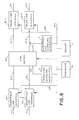
- The arrangement of the above-stated ATM switching system is constructed in a similar manner to conventional ISDN switching systems, and the processing of signalling therein, are described with reference to Fig. 9. In this figure, 11 (11-1 - 11-j) designates optical fibers having a transmission rate of, for example, about 150 Mbit/s; 10 (10-1 - 10-j) designates subscriber line interfaces which perform, for example, optical/electrical signal conversion; 30 designates an ATM switch for switching cells; 12 (12-1 - 12-j) designates 8-bit buses.
- Cell dropper/inserter circuits 16 (16-1 - 16-j) are inserted between the
subscriber line interfaces 10 and theATM switch 30. In receiving subsystems (from thesubscriber line interfaces 10 to the ATM switch 30), only cells in the signalling channels are separated and extracted, while in transmission subsystems (from theATM switch 30 to the subscriber line interfaces 10), signalling channel cells are inserted. Cell data from the cell dropper/inserter 16 is multiplexed by a multiplexer/demultiplexer (MUX) 17, and connected to a subscriberline signalling unit 1 via abus 19. The subscriberline signalling unit 1 comprises: a multiplexer/demultiplexer (MUX) 18, for multiplexing and demultiplexing cell data for each subscriber's line; the above-mentioned ADP processing units 100 (100-1 - 100-j); LAPD-LSI 101 (101-1 101-j), forprocessing layer 2 signalling channels; and abus 103. - In accordance with the above-mentioned system, a drawback exists in that one cell dropper/
inserter 16 is necessitated for each subscriber's line, andMUX 17 and buses for connecting them are further- required, since only cells in the signalling channels are collected. Further, theMUX 18 and ADP processing units for corresponding subscriber's lines must be provided in the subscriberline signalling unit 1. - An arrangement in which the subscriber line signalling apparatus and subscriber's terminals are interconnected by a switch is disclosed, for example, in Japanese Laid-open Patent Application No. 78637/1988. Such a system does not, however not contemplate any adaptation process and circuitry, such as a scanning unit, for subscriber lines necessary to detect signal frames.
- An advantage of the present invention is the provision of a system which provides a signalling apparatus for an ATM switching system which minimizes equipment requirements, thereby providing reduced cost, smaller size, and increased reliability.
- To solve the above-mentioned problems, the subject system provides the subscriber line signalling apparatus, including ADP processing units, on a trunk-line-side of the ATM switch. Collection and distribution of cells in the signalling channels are performed using the ATM switch, and the adaptation process is performed common to the subscriber's lines.
- In accordance with the present invention, the subscriber line signalling apparatus including ADP processing units is provided on the trunk-line-side of the ATM switch, and that the collection and distribution of cells in the signalling channels are performed using the ATM switch, whereby any cell dropper/inserter or cell multiplexer/demultiplexer is not necessitated. Also, since the adaptation process is performed common to all subscriber lines, the amount of hardware necessitated for the adaptation process can be reduced.
- In accordance with another aspect of the subject invention, the signalling apparatus is adapted with a trunk line signally apparatus placed on the subscriber line side of an ATM switch, working in concert with a subscriber line signally apparatus placed on a trunk line side of the ATM switch.
- The subject invention is described in conjunction with certain figures which are for purposes of illustrating the preferred embodiment of the invention only, and not for the purpose of limiting the same, wherein:
- Fig. 1 is a system block diagram showing a first embodiment of the present invention;
- Fig. 2 is a system block diagram showing a second embodiment of the present invention;
- Fig. 3 is a block diagram showing a transmission subsystem in an ADP processing unit;
- Fig. 4 is a block diagram showing a receiving subsystem in the
ADP processing unit 100; - Figs. 5(A) and 5(B) are diagrams for explaining a frame and a cell format;
- Fig. 6 is a diagram showing an exemplary arrangement of an ATM switching system applicable to Figs. 1, 2, 8, and 9;
- Fig. 7 is a table illustrating the conversion table memory of Fig. 6;
- Fig. 8 illustrates an embodiment of the subject invention employing a trunk side signalling processor;
- Fig. 9 is a system block diagram to which a conventional method of construction for a signalling apparatus is applied;
- Fig. 10 illustrates a fabrication scheme of the subject system;
- Fig. 11 illustrates an alternate fabrication scheme of the subject invention; and
- Fig. 12 illustrates an ATM switching network.
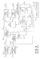
- Turning now to the drawings, Figs. 1 and 2, disclose an first embodiment of the present invention in which a subscriber
line signalling apparatus 1 includes anADP processing unit 100 for performing an adaptation process, including segmentation of a communication frame and reassembly of received cells. LAPD-LSI's 101 (101-1 - 101-l) for performlayer 2 protocol processing of a signalling channel. This apparatus is connected, via abus 15, to the trunk-line-side of anATM switch 30. A suitable ATM switch is taught in Also, the subscriberline signalling apparatus 1 is connected, via abus 103, to aprocessor 40 for performing, for example, the operation oflayer 3 protocol processing of signalling channels, and controlling of the LAPD-LSI's and initializing of an ATM switch. Numeral 11 (11-1 - 11-k) designates optical fibers, or the like, having a transmission rate of, for example, about 150 Mbits/s. Numeral 14 (14-1 - 14-k) designates optical fibers having a transmission rate of, for example, about 150 Mbits/s or 600 Mbits/s. Numeral 12 (12-1 12-j), 13 (13-1 - 13-k) and 15 are suitably formed of eight bit wide buses.Subscriber line interfaces 10 andtrunk line interfaces 20 suitably perform optical/electric signal conversion, and add/delete a route information segment to and from individual cells, respectively. - Although the
optical fibers buses - Numeral 30 designates an ATM switch for switching fixed length cells, and may be, for example, comprised of a switch of the type described in "A Memory Switch Architecture for ATM Switching Network," IEICE Technical Report IN88-38. Assuming that the numbers of input and output buses of the ATM switch are 32 and 32, respectively, j=32 and k=31 in the figures. If it is desired to have 32 input buses and 32 output buses for switching cells of information channels, then the ATM switch should be provided with 32 input buses and 33 or 34 output buses. One or two
buses 15 on the trunk-line-side should be exclusively used for signalling channels. - Though the embodiment of Fig. 1 has one LAPD-LSI for each subscriber line (j=1), the number of LAPD-LSI's may be reduced (j>1) or additional LAPD-LSI's may be provided (j<1) to provide against emergencies. Fig. 2 shows a system in which the process of
layer 2 of signalling channels for a plurality of subscriber lines (11-1 - 11-j) is performed by a single LAPD-LSI 101. - Fig. 3 is a block diagram showing the transmission system in the above-mentioned
ADP processing unit 100, and Fig. 4 is a block diagram of receiving system in theADP processing unit 100. - In the previously mentioned CCITT Draft Recommendation I.121, the final cell format (cell size, etc.) is not yet determined. Thus, a cell format shown in Fig. 5(B) is assumed in the ADP processing in Figs. 3 and 4. Each
cell 51 comprises 36 bytes and consists of acell header 52 of 4 bytes and aninformation field 53 of 32 bytes. Thecell header 52 includes first 12 bits which form a VCN (Virtual Channel Number) field for identification of the cell, areserved field 521 and an HCS (header Check Sequence)field 522 for detecting cell header abnormalities. At the head of theinformation field 53, there is anADP header 54 of 2 byte. Therefore, aregion 55 wherein frame data shown in Fig. 5(A) can be stored has 30 bytes for each cell. TheADP header 54 has: acell type region 542 of 2 bits indicating which type the cell is (i.e. beginning of frame, end of frame, middle of frame, or one-cell=one-frame), as shown in Fig. 5(C); aregion 543 of one byte indicating the effective information length of theinformation field 53; and areserved region 541. - For example, if the length between the
flags frame 50 in Fig. 5(A) is 6 bytes, then it can be segmented into a cell which is of the type "1 cell = 1 frame" having an effective information length of 6. If the frame length is 40 bytes, then it can be divided into two cells, namely, a first cell of the "beginning of frame" type having an effective information length of 30, and a second cell of the "end of frame" type having an effective information length of 10. - On the other hand, the
route information field 56 at the beginning of the cell of Fig. 5(B) is applied thereto only within the ATM switching system, and each cell is otherwise transmitted in a format lacking the above-mentionedroute information field 56 through thesubscriber lines 11 or through the trunk lines 14. The route information field is used to store therein information specifying the output line to which a cell switched in theATM switch 30 should be transmitted, and the subscriber line number, etc. - Next, details of the transmitting subsystem of the ADP processing unit will be described with reference to Fig. 3.
- A transmission line selector 110a has signal line sets 102a (102a-1 - 102a-j), each of which consist of three lines, namely, a transmission data (TXD), transmission clock (TXC) and echo (E) lines, and each of which is connected to a corresponding one of LAPD-LSI's 101 (101-1 - 101-j); the selector 110a has a function of collision control to extract only the frame of a specified line when a plurality of frames are simultaneously transmitted from a plurality of LAPD's. The D-channel access procedure, described in the CCITT Recommendation I.430, may be used as the procedure of the collision control. The line number selected in accordance with the collision control is communicate to a
CTL 190, while transmission data is transmitted to aframe detector 112. The transmission line selector 110a is necessary only in the first embodiment of the present invention. - The
frame detector 112 will communicate the DLCI (Data Link Connection Identifier) in theaddress field 50B of the frame to theCTL 190, and will arrange the data from the address field to FCS (Frame Check Sequence)field 50E into an 8-bit parallel data after deleting a '0' bit for flag identification, and transmit it to acounter 116. If the data is the last data of a frame, then such fact is communicated to thecounter 116 through a final notice signal line. - The
counter 116 will transfer the frame data to an FIFO-A 120. When the FIFO-A has been filled by 30 byte data transferred thereto, or the last data of a frame has been transferred thereto, thecell type 542 and theeffective information length 543 shown in the ADP header format of Fig. 5(B) are communicated to theCTL 190, and thereafter it will transfer data from theframe detector 112 to an FIFO-B 121. When the FIFO B has been filled up or the last frame data has been transferred thereto during transfer of data to the FIFO-B, thecounter 116 will likewise communicate the cell type and the effective information length to theCTL 190, and will transfer subsequent data to the FIFO-A 120. In the manner as described, the FIFO-A and FIFO-B are alternately used. - The
CTL 190 is constituted by, for example, µCPU's, ROM's and RAM's, and contains a DLCI/header corresponding table 191, in which contents of headers (all of the 10 bytes from theroute information 56 to theADP header 54 in Fig. 5(B)) corresponding to the combinations of line numbers and DLCI are set from outside via acontrol bus 103. TheCTL 190 will search the DLCI/header corresponding table 191 upon receiving the communication of the line number and the DLCI, and write the contents of the corresponding table onto aheader register 118. - In the second embodiment of the present invention, however, after the DLCI/header corresponding table has been searched, the unique DLCI is converted, using a DLCI conversion table 195, into a DLCI which is actually transmitted to a subscriber device. Subsequently, upon receipt of the communication of the cell type and effective information length from the
counter 116, a corresponding register, within aheader register 118, is rewritten in accordance with anADP header format 54 of Fig. 5(B) and a selector (SEL) 122 is activated. - The
SEL 122 will first transmit the data in aheader register 118, and will next transmit the data in the FIFO-A 120, thereby completing the transmission of the cell. Subsequently, when receiving an activation from the CTL, theSEL 122 will transmit the data in theheader register 118, and will then transmit the data in the FIFO-B 121, thereby completing the transmission of the cell. Subsequently, theSEL 122 will transmit the data FIFO-A and the data in the FIFO-B alternately. - Meanwhile, an amount to be processed for forming a header for the transmission of a cell can be reduced by arranging such that the searching of the DLCI/header corresponding table 191 and the setting of the ADP header in the header register are performed separately in the CTL and a reading of the data in the
header register 118 will not change such data. For example, when a frame is divided into a plurality of cells for transmission, it is not necessary to search the DLCI/header corresponding table 191 for each cell if the arrangement is such that the searching of the DLCI/header corresponding table is performed only for transmitting the cell at the beginning of the frame and, for the subsequent cells, only the ADP header in theheader register 118 is rewritten. - Next, details of the receiving subsystem of the ADP processing unit will be described with reference to Fig. 4. Therein, a
cell writing unit 124 is connected with theATM switch 30 through a receiving bus 15b for receiving cells of a signalling channel from a subscriber unit. The received cell data is transferred to an empty area of a first buffer BF in abuffer memory 126 according to an address indicated by a WA (Write Address) register 125 within thecell writer 124. Subsequently, the data in anempty address FIFO 130 is set in theWA 125 for preparation for receiving the next cell. - The buffer memory 126 (BFM) comprises the first buffer BF of the form of an FIFO for receiving and temporarily storing therein cells arriving there at a rate of, for example, 150 Mbit/s; and second buffers BF-l - BF-n of an FIFO from prepared for respective combinations of line numbers and VCN in cell headers for the subsequent reassembling process. The construction of the BF of the form of FIFO, the manner of using a chain pointer, and the manner of using the WA register 125, RA (Read Address)
register 192, and theempty address FIFO 130 are described in the previously mentioned literature "A Memory Switch Architecture for ATM Switching Network". - A
CTL 190 has anRA register 192 which corresponds to the first buffer BF, and will check the line number, the VCN in the cell header and the cell type in the ADP header among the contents of the cell of the address indicated by the RA, and will first transfer such cell data to a second buffer BF-i which has the combination of the corresponding line number and VCN. In this case, an actual data transfer from memory to memory is not performed but transfer is performed only by rewriting a second buffer address table 193 provided in theCTL 190 and further rewriting the buffer chain pointer. If checking of the cell type in the ADP header shows that all cells of one frame has been received, then the top address of the buffer wherein the top cell of the frame is stored and the line number is written in a transferorder storing FIFO 194. TheCTL 190 will activate a P/S unit 128 in accordance with the data in the transferorder storing FIFO 194 and at the same time specify an output line number to a receipt line selector 110b. In the second embodiment of the present invention, when the P/S unit is activated, a unique DLCI is derived, using a DLCI conversion table 195, from the DLCI from a subscriber unit, and the unique DLC is simultaneously communicated to the P/S unit. - The P/
S unit 128 will read the data of the specified address in response to an activation from theCTL 190, and will convert data other than the header field into a serial data and will transfer such data to the receipt line selector 110b after insertion thereto of "0" and adding a frame delimitingcell type flag - The receipt line selector 110b is connected with LAPD-LSI 101 (101-1 - 101-j), via signal line sets 102b (102b-1 - 102b-j), each of which consists of two lines, namely, a receipt data line (RxD) and a receipt clock (RxC), and has a function of transmitting data only to a signal line having a line number specified by the
CTL 190. Meanwhile, the receipt line selector 110b is, as is the transmission line selector shown in Fig. 3, necessitated only in the arrangement of the first embodiment and not necessary in the arrangement of the second embodiment. - Though the above embodiment are arranged to control each hardware in the ADP processing unit by means of the
CTL unit 190 which uses a µCPU, it is also possible to increase the processing rate by implementation all the functions of the CTL by hardware. In such case, in Fig. 4, the first buffer BF for rate adaptation (waiting) may be omitted, and the contents of the header may be checked in the cell writer and the cell data may be directly transferred to the second buffers BF-l - BF-n. - Where management of VCN is performed for each subscriber line separately from the others, different subscribers can simultaneously transmit cells having the same VCN. Then, in accordance with a system in which an ADP processing unit is provided common to a plurality of subscriber lines, identification of cells only from the VCN will mix cells from different subscribers, with the result that reassembling cannot normally performed. In accordance with the present invention, when a cell is received from a subscriber,
route information 56 is added to the cell, where the subscriber line number is stored, and further in the ADP processing unit receipt system the cell is identified from such subscriber line number and the VCN, whereby reassembling can be normally performed. Further, the arrangement may be such that the subscriber line number is not recorded, and the VCN of the cell is converted in thesubscriber line interface 10 into a VCN unique to the VCN used forsubscriber lines 1 ... j. Further, where the management of DLCI is performed for each subscriber line separately from the others, different subscribers can simultaneously use the same DLCI. Then, in accordance with the arrangement of the second embodiment (Fig. 2), wherein a LAPD-LSI is provided common to a plurality of subscriber lines, two or more links having the same DLCI for different subscribers cannot be discriminated. In this case, links can be normally discriminated if the arrangement is such that a DLCI conversion table is provided in theADP processing unit 100 and, between the LAPD-LSI 101 and theADP processing unit 100, unique DLCI's are used for thesubscriber lines 1 ... j. - Turning now to Fig. 6, with continued reference to Fig. 5, shown in detail is construction of the subscriber line interface 10-i. The subscribe line interface 10-i communicates
route information 56 from eachcell 51 inputted from theATM switch 30 throughreception bus 12A, a parallel/serial (P/S)converter 202 for converting parallel data of the input cell which has no route information to bit serial data, and electrical/optical (E/O)signal converter 203 for converting the bit serial data to optical signals. - The subscriber line interface 10-i further comprises an optical/electrical (O/E)
signal converter 204 for converting optical signals transmitted from a subscriber terminal onto a transmission optical fiber 11B to bit serial electrical signals, a serial/parallel (S/P)converter 205 for converting the bit serial signal to 8-bit parallel data, aheader separator circuit 206, aheader inserter circuit 207, and a headerconversion table memory 208. - As stated hereinbefore, each cell transmitted from the subscriber terminal includes a
cell header 52 and aninformation field 53 as shown in Fig. 5B. Theheader separator circuit 206 operates to separate thecell header 52 from the received cell in order to access the header conversion table 208 in accordance with the value of field VCN extracted from the header, and to provide theinformation field 53 of the received cell to theheader inventer circuit 207. - The header conversion table means 208 stores a plurality of records, each of which comprises
route information 56, and anew header 52 including anew VCN 520 as shown in Fig. 7. One of these records is read out to theheader inserter circuit 207 by addressing in accordance with the extracted VCN. Theheader inserter circuit 207 operates to output a header converted cell which has aroute information field 56 and anew cell header 52 onto atransmission bus 12B. - If an input (extracted) VCN has a value corresponding to the signalling channel, a record which includes route information to designate the
bus 15 as an output port is read out. If the input VCN corresponds to an information channel, a record which designates one of output busses 13-1 through 13-k is read out. The contents of the headerconversion table memory 208 are prepared by theprocessor 40 through abus 104. - Fig. 8 shows a third embodiment of the present invention. In this embodiment, a signalling control system, the same as that which is adopted in the first or second embodiment is also applied to the trunk line signal processing. A trunk
line signalling apparatus 2 has substantially the same construction as the line signalling apparatus shown in Figs. 1 or 2. - In Fig. 8, signalling channel cells transmitted from the subscriber terminal are relayed to the
bus 15 by theATM switch 30. A reassembly process from cell(s) to a frame and thelayer 2 process are performed by the subscriber line signalling apparatus, whereby a signalling channel message extracted from the reassembled frame is supplied to theprocessor 40. Each trunk line interface (20-1 - 20-k) may have the same construction as the subscriber line interface shown in Fig. 6. - Similar to this process, signalling channel cells transmitted from another ATM switch through one of the optical fibers 14-l through 14-k are relayed to a
bus 25 by theATM switch 30 and inputted to the trunkline signalling apparatus 2. The trunkline signalling apparatus 2 performs the reassembling from the received cells to a frame and thelevel 2 process, so that a signalling channel message extracted from the reassembled frame is also supplied to theprocessor 40. - The
processor 40 performs alayer 3 process as to the signalling channel message supplied from the signallingapparatuses processor 40 suitably communicates a request for transmitting the new message to the trunk line signalling apparatus. The trunk line signalling apparatus performs thelayer 2 processing and the segmenting process as to the new message, and sends out a series of new cells thus produced to theATM switch 30 through thebus 25. - These cells are relayed to one of the trunk line buses 13-l through 13-k according to their route information which is added by the ADP processing unit in the trunk line signalling apparatus.
- Each of the trunk line interfaces 20-1 through 20-k is provided with a header conversion table memory namely as the subscriber line interface 10-i shown in Fig. 8. The contents of the table are also managed by the processor via a
bus line 105. - As is clear from the above description, the subscriber line signalling apparatus is provided on the trunk-line-side of an ATM switch in an ATM switching system according to the present invention, and an ADP processing unit is provided common to the subscriber lines, whereby advantages can be achieved in that the cell dropper/inserters, one for each subscriber line, buses for line collection/distribution or multiplexer/demultiplexers necessitated in a subscriber line signalling apparatus constructed in a similar manner to prior art ISDN switching systems can be omitted and the ADP processing units can be reduced in number, so that the amount of hardware can be reduced.
Claims (20)
interface means for communicating cell data with a transmission line;
an asynchronous transfer mode switching means operatively connected to the interface means for communicating cell data therewith;
the switching means including means for intercepting signalling channel data cells;
means for communicating signalling channel data cells with a subscriber line signalling apparatus;
the subscriber line signalling apparatus including,
an adaptation processing unit for performing at least one of reassembly and segmentation of cell data to frame data,
a data link processing means for processing frame data, and
means for communicating frame data between the link access processing means and an associated data processing element.
means for detecting frame data;
buffer means for apportioning cell data in fixed length increments from the frame data;
means for means for queuing the cell data in fixed length increments;
means for isolating cell identification information;
means for appending the cell identification information to the cell data in fixed length increments; and
means for communicating the cell data to the asynchronous transfer mode switching means.
means for detecting a series of data frames;
means for storing frame data within the series of data frames;
means for detecting a completion of a series of data frames; and
means for communicating the cell data to the asynchronous transfer mode switching means upon a detection of a completed series of data frames.
means for receiving a sequence of data cells from the asynchronous transfer mode switching means;
means for separating cell data from identification information appended thereto;
means for acquiring address information from an associated data processing unit;
means for accumulating the cell data;
means for computing data link communication identifier data from the cell identification information and the address information;
means for appending the data link communication identifier to the accumulated cell data to form frame data; and
means for communicating the frame data to the link access processing means.
communicating cell data with a transmission line to an asynchronous transfer mode switching means;
intercepting signalling channel data cells in the asynchronous mode switching means;
communicating signalling channel data cells with a subscriber line signalling apparatus;
performing at least one of reassembly and segmentation of cell data to frame data;
processing frame data for communication to a an associated data processing element, and
communicating processed frame data between the link access processing means and the associated data processing element.
detecting the presence of frame data;
apportioning cell data in fixed length increments from the frame data;
queuing the cell data in fixed length increments;
isolating cell identification information;
appending the cell identification information to the cell data in fixed length increments; and
communicating the cell data to the asynchronous transfer mode switching means.
detecting a series of data frames;
storing frame data for an series of data frames;
detecting a completion of a series of data frames; and
communicating the cell data to the asynchronous transfer mode switching means upon detection of a completed series of data frames.
receiving a sequence of data cells from the asynchronous transfer mode switching means;
separating cell data from identification information appended thereto;
acquiring address information from an associated data processing unit;
accumulating the cell data;
computing data link communication identifier data from the cell identification information and the address information;
appending the data link communication identifier to the accumulated cell data to form frame data; and
communicating the frame data to the link access processing means.
a switching circuit having a plurality of input terminals and a plurality of output-terminals, the switching circuit including means for directing a series of fixed length information packets in input terminals thereof to a selected output terminal thereof;
a signalling frame processor for communicating a signal frame to an associated data processing element; and
an adaptation processing unit for receiving fixed length information packets from an output of the switching circuit, the adaptation processing unit including means for communicating the fixed length information packets to the signal frame processor.
means for providing an information field, including a subscriber circuit number, to each of the fixed length packets; and
wherein the adaptation processing unit includes means for channelling data of in information packet to a selected subscriber line in accordance with the information field.
interface means for communicating cell data with an input transmission line;
an asynchronous transfer mode switching means operatively connected to the interface means for communicating cell data therewith;
means for communicating cell data between the asynchronous transfer mode switching means and a subscriber line signalling apparatus;
the subscriber line signalling apparatus including, an adaptation processing unit for performing assembly of cell data to frame data,
a data link processing means for processing frame data, and
means for communicating frame data between the link access processing means and an associated data processing element; means for communicating frame data from the associated data processing element to a trunk line signalling apparatus;
the trunk line signalling apparatus including an adaptation processing unit for performing segmentation of frame data to assembled cell data; and
means for communicating assembled cell data between the trunk line signal processing apparatus and the asynchronous transfer mode switching means.
Applications Claiming Priority (3)
| Application Number | Priority Date | Filing Date | Title |
|---|---|---|---|
| JP210718/88 | 1988-08-26 | ||
| JP21071888 | 1988-08-26 | ||
| JP21071888 | 1988-08-26 |
Publications (4)
| Publication Number | Publication Date |
|---|---|
| EP0355797A2 true EP0355797A2 (en) | 1990-02-28 |
| EP0355797A3 EP0355797A3 (en) | 1991-02-06 |
| EP0355797B1 EP0355797B1 (en) | 1995-03-15 |
| EP0355797B2 EP0355797B2 (en) | 2001-03-21 |
Family
ID=16593951
Family Applications (1)
| Application Number | Title | Priority Date | Filing Date |
|---|---|---|---|
| EP89115476A Expired - Lifetime EP0355797B2 (en) | 1988-08-26 | 1989-08-22 | Signalling apparatus for use in an ATM switching system |
Country Status (3)
| Country | Link |
|---|---|
| EP (1) | EP0355797B2 (en) |
| JP (2) | JP3132564B2 (en) |
| DE (1) | DE68921685T3 (en) |
Cited By (12)
| Publication number | Priority date | Publication date | Assignee | Title |
|---|---|---|---|---|
| FR2659513A1 (en) * | 1990-03-12 | 1991-09-13 | Cit Alcatel | SUBSCRIBER TERMINAL INSTALLATION FOR ASYNCHRONOUS NETWORKS. |
| EP0467330A2 (en) * | 1990-07-17 | 1992-01-22 | Fujitsu Limited | Signalling data receiving and processing unit provided in a broadband integrated services digital network |
| FR2670974A1 (en) * | 1990-12-20 | 1992-06-26 | Lmt Radio Professionelle | DEVICE FOR THE TRANSMISSION BY AN ASYNCHRONOUS NETWORK, IN PARTICULAR AN ATM TYPE NETWORK, OF SIGNALING DATA BY WAY REGROUGH INTO A MULTICHRONOUSLY SYNCHRONOUSLY CONFERRED MULTIPARTY. |
| EP0528370A2 (en) * | 1991-08-15 | 1993-02-24 | Fujitsu Limited | Frame length control in data transmission using ATM network |
| EP0531599A1 (en) * | 1991-09-13 | 1993-03-17 | International Business Machines Corporation | Configurable gigabit/s switch adapter |
| EP0584398A1 (en) * | 1992-08-28 | 1994-03-02 | Siemens Aktiengesellschaft | Method and circuit to transmit information cells within an ATM network |
| EP0632945A1 (en) * | 1992-03-23 | 1995-01-11 | Motorola, Inc. | Packet reassembly method and apparatus |
| FR2707820A1 (en) * | 1993-07-15 | 1995-01-20 | Cit Alcatel | Digital link interface circuit for a switching centre terminal unit with asynchronous transfer mode |
| EP0715470A2 (en) * | 1991-05-14 | 1996-06-05 | Fujitsu Limited | System for supplying a plurality of ATM cells |
| WO1996019059A2 (en) * | 1994-12-16 | 1996-06-20 | Tony Walker | Packet based data transmission system |
| EP0820209A2 (en) * | 1996-07-17 | 1998-01-21 | Matsushita Electric Industrial Co., Ltd. | Data transfer device having retransmission control function |
| WO1999001009A2 (en) * | 1997-06-27 | 1999-01-07 | Nokia Networks Oy | Processing of signalling messages in atm node |
Families Citing this family (3)
| Publication number | Priority date | Publication date | Assignee | Title |
|---|---|---|---|---|
| JPH02228838A (en) * | 1989-03-02 | 1990-09-11 | Oki Electric Ind Co Ltd | Interface circuit |
| CA2049428C (en) * | 1990-08-20 | 1996-06-18 | Yasuro Shobatake | Atm communication system |
| JP2577524B2 (en) * | 1993-07-13 | 1997-02-05 | 日本電気株式会社 | Cell exchange |
Citations (4)
| Publication number | Priority date | Publication date | Assignee | Title |
|---|---|---|---|---|
| WO1984000265A1 (en) * | 1982-06-25 | 1984-01-19 | Western Electric Co | Fast packet switch |
| EP0183592A1 (en) * | 1984-11-08 | 1986-06-04 | LABORATOIRE CENTRAL DE TELECOMMUNICATIONS Société anonyme: | Asynchronous packet switch |
| US4611322A (en) † | 1984-08-03 | 1986-09-09 | At&T Bell Laboratories | Traffic load control arrangement and method for a packet switching system |
| GB2184327A (en) * | 1985-12-13 | 1987-06-17 | American Telephone & Telegraph | Digital communication network architecture for providing universal information services |
-
1989
- 1989-06-21 JP JP15677289A patent/JP3132564B2/en not_active Expired - Lifetime
- 1989-08-22 EP EP89115476A patent/EP0355797B2/en not_active Expired - Lifetime
- 1989-08-22 DE DE68921685T patent/DE68921685T3/en not_active Expired - Fee Related
-
2000
- 2000-05-12 JP JP2000144585A patent/JP2000349790A/en active Pending
Patent Citations (4)
| Publication number | Priority date | Publication date | Assignee | Title |
|---|---|---|---|---|
| WO1984000265A1 (en) * | 1982-06-25 | 1984-01-19 | Western Electric Co | Fast packet switch |
| US4611322A (en) † | 1984-08-03 | 1986-09-09 | At&T Bell Laboratories | Traffic load control arrangement and method for a packet switching system |
| EP0183592A1 (en) * | 1984-11-08 | 1986-06-04 | LABORATOIRE CENTRAL DE TELECOMMUNICATIONS Société anonyme: | Asynchronous packet switch |
| GB2184327A (en) * | 1985-12-13 | 1987-06-17 | American Telephone & Telegraph | Digital communication network architecture for providing universal information services |
Non-Patent Citations (1)
| Title |
|---|
| ICC-87, Session 22, Paper 2, vol. 2, 07 June 1987, Seattle, US pages 1 - 5; J.P.Coudreuse et al: "PRELUDE: An asynchronous time-division switched network" * |
Cited By (30)
| Publication number | Priority date | Publication date | Assignee | Title |
|---|---|---|---|---|
| AU641733B2 (en) * | 1990-03-12 | 1993-09-30 | Alcatel N.V. | Subscriber terminal for an asynchronous network |
| EP0446827A1 (en) * | 1990-03-12 | 1991-09-18 | Alcatel Cit | Terminal installation for asynchronous network |
| FR2659513A1 (en) * | 1990-03-12 | 1991-09-13 | Cit Alcatel | SUBSCRIBER TERMINAL INSTALLATION FOR ASYNCHRONOUS NETWORKS. |
| US5170272A (en) * | 1990-03-12 | 1992-12-08 | Alcatel Cit | Subscriber terminal installation for an asynchronous network |
| EP0467330A2 (en) * | 1990-07-17 | 1992-01-22 | Fujitsu Limited | Signalling data receiving and processing unit provided in a broadband integrated services digital network |
| EP0467330A3 (en) * | 1990-07-17 | 1995-01-04 | Fujitsu Ltd | Signalling data receiving and processing unit provided in a broadband integrated services digital network |
| US5220563A (en) * | 1990-12-20 | 1993-06-15 | Thomson-Csf | Device for the transmission by an asynchronous network, notably an atm type network, of signalling data, channel by channel, assembled in a multiframe transmitted synchronously in out-of-band mode |
| EP0493176A1 (en) * | 1990-12-20 | 1992-07-01 | Thomson-Csf | Device for transmitting in an asynchronous network, especially an ATM-network, channel-by-channel signalling data gathered in a multiframe synchronously transmitted out-of-band |
| FR2670974A1 (en) * | 1990-12-20 | 1992-06-26 | Lmt Radio Professionelle | DEVICE FOR THE TRANSMISSION BY AN ASYNCHRONOUS NETWORK, IN PARTICULAR AN ATM TYPE NETWORK, OF SIGNALING DATA BY WAY REGROUGH INTO A MULTICHRONOUSLY SYNCHRONOUSLY CONFERRED MULTIPARTY. |
| EP0715470A2 (en) * | 1991-05-14 | 1996-06-05 | Fujitsu Limited | System for supplying a plurality of ATM cells |
| EP0715470A3 (en) * | 1991-05-14 | 1996-08-14 | Fujitsu Ltd | System for supplying a plurality of ATM cells |
| EP0528370A2 (en) * | 1991-08-15 | 1993-02-24 | Fujitsu Limited | Frame length control in data transmission using ATM network |
| EP0528370A3 (en) * | 1991-08-15 | 1994-11-09 | Fujitsu Ltd | Frame length control in data transmission using atm network |
| US5535221A (en) * | 1991-08-15 | 1996-07-09 | Fujitsu Limited | Frame length control in data transmission using ATM network |
| EP0531599A1 (en) * | 1991-09-13 | 1993-03-17 | International Business Machines Corporation | Configurable gigabit/s switch adapter |
| US5311509A (en) * | 1991-09-13 | 1994-05-10 | International Business Machines Corporation | Configurable gigabits switch adapter |
| EP0632945A1 (en) * | 1992-03-23 | 1995-01-11 | Motorola, Inc. | Packet reassembly method and apparatus |
| EP0632945A4 (en) * | 1992-03-23 | 1999-09-29 | Motorola Inc | Packet reassembly method and apparatus. |
| EP0584398A1 (en) * | 1992-08-28 | 1994-03-02 | Siemens Aktiengesellschaft | Method and circuit to transmit information cells within an ATM network |
| US5394398A (en) * | 1992-08-28 | 1995-02-28 | Siemens Aktiengesellschaft | Method and circuit arrangement for the transmission of message cells within an ATM network |
| FR2707820A1 (en) * | 1993-07-15 | 1995-01-20 | Cit Alcatel | Digital link interface circuit for a switching centre terminal unit with asynchronous transfer mode |
| WO1996019059A3 (en) * | 1994-12-16 | 1996-09-06 | Tony Walker | Packet based data transmission system |
| US5613069A (en) * | 1994-12-16 | 1997-03-18 | Tony Walker | Non-blocking packet switching network with dynamic routing codes having incoming packets diverted and temporarily stored in processor inputs when network ouput is not available |
| WO1996019059A2 (en) * | 1994-12-16 | 1996-06-20 | Tony Walker | Packet based data transmission system |
| EP0820209A2 (en) * | 1996-07-17 | 1998-01-21 | Matsushita Electric Industrial Co., Ltd. | Data transfer device having retransmission control function |
| EP0820209A3 (en) * | 1996-07-17 | 1999-12-22 | Matsushita Electric Industrial Co., Ltd. | Data transfer device having retransmission control function |
| WO1999001009A2 (en) * | 1997-06-27 | 1999-01-07 | Nokia Networks Oy | Processing of signalling messages in atm node |
| WO1999001009A3 (en) * | 1997-06-27 | 1999-03-18 | Nokia Telecommunications Oy | Processing of signalling messages in atm node |
| AU737949B2 (en) * | 1997-06-27 | 2001-09-06 | Nokia Networks Oy | Processing of signalling messages in ATM node |
| US6731641B1 (en) * | 1997-06-27 | 2004-05-04 | Nokia Corporation | Processing of signalling messages in ATM node |
Also Published As
| Publication number | Publication date |
|---|---|
| JPH02140037A (en) | 1990-05-29 |
| DE68921685D1 (en) | 1995-04-20 |
| DE68921685T3 (en) | 2001-06-13 |
| JP3132564B2 (en) | 2001-02-05 |
| EP0355797B1 (en) | 1995-03-15 |
| EP0355797A3 (en) | 1991-02-06 |
| EP0355797B2 (en) | 2001-03-21 |
| JP2000349790A (en) | 2000-12-15 |
| DE68921685T2 (en) | 1995-07-27 |
Similar Documents
| Publication | Publication Date | Title |
|---|---|---|
| US5101404A (en) | Signalling apparatus for use in an ATM switching system | |
| US5303236A (en) | Signalling apparatus for use in an ATM switching system | |
| JP2890348B2 (en) | Telephone subscriber accommodation in broadband networks. | |
| US6031838A (en) | ATM switching system | |
| US5214642A (en) | ATM switching system and adaptation processing apparatus | |
| EP0858240B1 (en) | Cell assembly and multiplexing device, and demultiplexing device | |
| EP0355797B2 (en) | Signalling apparatus for use in an ATM switching system | |
| US6618374B1 (en) | Method for inverse multiplexing of ATM using sample prepends | |
| JP3189954B2 (en) | Asynchronous cell switching system | |
| JPH0522403A (en) | Stm-atm mutual conversion control system0 | |
| JPH07202895A (en) | System and device for cell multiplexing | |
| JP3055547B2 (en) | Cell assembling method, cell disassembling method, and ATM cell communication device | |
| JP2785005B2 (en) | Multiplexing / demultiplexing method in FC / ATM network interconversion equipment | |
| JP3055548B2 (en) | ATM communication device | |
| JP3129301B2 (en) | ATM switch | |
| JP3129300B2 (en) | ATM switch | |
| JPH05252190A (en) | Atm communication equipment and cell band control method | |
| JP2785006B2 (en) | Multiplexing / demultiplexing method in FC / ATM network interconversion equipment | |
| JP3014619B2 (en) | Asynchronous transfer mode communication system, cell disassembly apparatus therefor, and asynchronous transfer mode communication method | |
| KR100354178B1 (en) | ATM Cell Multiplexing Apparatus Using Multi-Subscriber Link Interface | |
| JPH1146200A (en) | Atm exchange | |
| JPH08331155A (en) | Atm exchange | |
| JPH1146201A (en) | Atm communication system | |
| JPH08331156A (en) | Method for assembling cell, method for disassembling cell and atm cell | |
| KR100236038B1 (en) | Multiplexer and demultiplexer for directly interfacing external image signals in an atm card |
Legal Events
| Date | Code | Title | Description |
|---|---|---|---|
| PUAI | Public reference made under article 153(3) epc to a published international application that has entered the european phase |
Free format text: ORIGINAL CODE: 0009012 |
|
| AK | Designated contracting states |
Kind code of ref document: A2 Designated state(s): DE FR GB |
|
| PUAL | Search report despatched |
Free format text: ORIGINAL CODE: 0009013 |
|
| 17P | Request for examination filed |
Effective date: 19901212 |
|
| AK | Designated contracting states |
Kind code of ref document: A3 Designated state(s): DE FR GB |
|
| RHK1 | Main classification (correction) |
Ipc: H04Q 11/04 |
|
| 17Q | First examination report despatched |
Effective date: 19930906 |
|
| GRAA | (expected) grant |
Free format text: ORIGINAL CODE: 0009210 |
|
| AK | Designated contracting states |
Kind code of ref document: B1 Designated state(s): DE FR GB |
|
| REF | Corresponds to: |
Ref document number: 68921685 Country of ref document: DE Date of ref document: 19950420 |
|
| ET | Fr: translation filed | ||
| PLBQ | Unpublished change to opponent data |
Free format text: ORIGINAL CODE: EPIDOS OPPO |
|
| PLBI | Opposition filed |
Free format text: ORIGINAL CODE: 0009260 |
|
| 26 | Opposition filed |
Opponent name: NOKIA TELECOMMUNICATIONS OY Effective date: 19951215 Opponent name: ALCATEL N.V. Effective date: 19951213 |
|
| PLBF | Reply of patent proprietor to notice(s) of opposition |
Free format text: ORIGINAL CODE: EPIDOS OBSO |
|
| PLBF | Reply of patent proprietor to notice(s) of opposition |
Free format text: ORIGINAL CODE: EPIDOS OBSO |
|
| PLBF | Reply of patent proprietor to notice(s) of opposition |
Free format text: ORIGINAL CODE: EPIDOS OBSO |
|
| PLBQ | Unpublished change to opponent data |
Free format text: ORIGINAL CODE: EPIDOS OPPO |
|
| PLAB | Opposition data, opponent's data or that of the opponent's representative modified |
Free format text: ORIGINAL CODE: 0009299OPPO |
|
| R26 | Opposition filed (corrected) |
Opponent name: ALCATEL N.V. * 19951215 NOKIA TELECOMMUNICATIONS O Effective date: 19951213 |
|
| PLAW | Interlocutory decision in opposition |
Free format text: ORIGINAL CODE: EPIDOS IDOP |
|
| PLAW | Interlocutory decision in opposition |
Free format text: ORIGINAL CODE: EPIDOS IDOP |
|
| PUAH | Patent maintained in amended form |
Free format text: ORIGINAL CODE: 0009272 |
|
| STAA | Information on the status of an ep patent application or granted ep patent |
Free format text: STATUS: PATENT MAINTAINED AS AMENDED |
|
| 27A | Patent maintained in amended form |
Effective date: 20010321 |
|
| AK | Designated contracting states |
Kind code of ref document: B2 Designated state(s): DE FR GB |
|
| ET3 | Fr: translation filed ** decision concerning opposition | ||
| REG | Reference to a national code |
Ref country code: GB Ref legal event code: IF02 |
|
| PGFP | Annual fee paid to national office [announced via postgrant information from national office to epo] |
Ref country code: FR Payment date: 20060802 Year of fee payment: 18 |
|
| PGFP | Annual fee paid to national office [announced via postgrant information from national office to epo] |
Ref country code: GB Payment date: 20060808 Year of fee payment: 18 |
|
| PGFP | Annual fee paid to national office [announced via postgrant information from national office to epo] |
Ref country code: DE Payment date: 20060828 Year of fee payment: 18 |
|
| GBPC | Gb: european patent ceased through non-payment of renewal fee |
Effective date: 20070822 |
|
| REG | Reference to a national code |
Ref country code: FR Ref legal event code: ST Effective date: 20080430 |
|
| PG25 | Lapsed in a contracting state [announced via postgrant information from national office to epo] |
Ref country code: DE Free format text: LAPSE BECAUSE OF NON-PAYMENT OF DUE FEES Effective date: 20080301 |
|
| PG25 | Lapsed in a contracting state [announced via postgrant information from national office to epo] |
Ref country code: FR Free format text: LAPSE BECAUSE OF NON-PAYMENT OF DUE FEES Effective date: 20070831 |
|
| PG25 | Lapsed in a contracting state [announced via postgrant information from national office to epo] |
Ref country code: GB Free format text: LAPSE BECAUSE OF NON-PAYMENT OF DUE FEES Effective date: 20070822 |