EP0361153A2 - Arrangement for coupling an optical fibre with a coupling window of a planar integrated optical device, and method for making such an arrangement - Google Patents
Arrangement for coupling an optical fibre with a coupling window of a planar integrated optical device, and method for making such an arrangement Download PDFInfo
- Publication number
- EP0361153A2 EP0361153A2 EP89116456A EP89116456A EP0361153A2 EP 0361153 A2 EP0361153 A2 EP 0361153A2 EP 89116456 A EP89116456 A EP 89116456A EP 89116456 A EP89116456 A EP 89116456A EP 0361153 A2 EP0361153 A2 EP 0361153A2
- Authority
- EP
- European Patent Office
- Prior art keywords
- coupling
- substrate
- fiber
- coupling window
- arrangement
- Prior art date
- Legal status (The legal status is an assumption and is not a legal conclusion. Google has not performed a legal analysis and makes no representation as to the accuracy of the status listed.)
- Ceased
Links
Images
Classifications
-
- G—PHYSICS
- G02—OPTICS
- G02B—OPTICAL ELEMENTS, SYSTEMS OR APPARATUS
- G02B6/00—Light guides; Structural details of arrangements comprising light guides and other optical elements, e.g. couplings
- G02B6/24—Coupling light guides
- G02B6/42—Coupling light guides with opto-electronic elements
- G02B6/4201—Packages, e.g. shape, construction, internal or external details
- G02B6/4202—Packages, e.g. shape, construction, internal or external details for coupling an active element with fibres without intermediate optical elements, e.g. fibres with plane ends, fibres with shaped ends, bundles
-
- G—PHYSICS
- G02—OPTICS
- G02B—OPTICAL ELEMENTS, SYSTEMS OR APPARATUS
- G02B6/00—Light guides; Structural details of arrangements comprising light guides and other optical elements, e.g. couplings
- G02B6/24—Coupling light guides
- G02B6/26—Optical coupling means
- G02B6/30—Optical coupling means for use between fibre and thin-film device
-
- G—PHYSICS
- G02—OPTICS
- G02B—OPTICAL ELEMENTS, SYSTEMS OR APPARATUS
- G02B6/00—Light guides; Structural details of arrangements comprising light guides and other optical elements, e.g. couplings
- G02B6/24—Coupling light guides
- G02B6/42—Coupling light guides with opto-electronic elements
- G02B6/4201—Packages, e.g. shape, construction, internal or external details
- G02B6/4219—Mechanical fixtures for holding or positioning the elements relative to each other in the couplings; Alignment methods for the elements, e.g. measuring or observing methods especially used therefor
- G02B6/4228—Passive alignment, i.e. without a detection of the degree of coupling or the position of the elements
- G02B6/423—Passive alignment, i.e. without a detection of the degree of coupling or the position of the elements using guiding surfaces for the alignment
Definitions
- the invention relates to an arrangement for coupling an optical fiber to a coupling window of a planar integrated optical component according to the preamble of claim 1 and a method for producing such an arrangement.
- the properties of a fiber optic signal transmission link are determined by the quality of the optical coupling of the glass fiber to the transmit and receive modules. Since the light wave guided in the fiber generally has a lateral mode expansion in the ⁇ m range, a correspondingly precise adjustment of the elements relative to one another is necessary. With single-mode, integrated waveguides on III-IV semiconductors, the permissible lateral adjustment tolerances can also shrink to well below 1 ⁇ m due to the shortness of the light wavelength in the material.
- the fiber and the optical component to be coupled are each mounted on a subcarrier, together with the coupling optics required to adapt the mode. It can consist of a fiber taper with a lens attached (see Siemens Research and Development Report, vol. 13, (1984) pp. 284-288) or a spherical or gradient lens (see also Siemens Research and Development Reports, vol. 16 (1987 ) Pp. 141-146).
- the sub-units defined in this way are then soldered directly to one another relative to one another during adjustment on the main carrier. The possibility of using this method to first check the subunits separately and readjust them during assembly can be an advantage, but it must be be paid for with space requirements per coupling point and installation effort.
- the object of the invention is to provide a compact, easily mountable arrangement for coupling an optical fiber to a coupling window of a planar integrated component, in particular a planar integrated waveguide, which can be formed directly on the substrate on which the optical component is integrated.
- the guide channel according to the invention represents a support structure for the glass fiber that can be produced by monolithic integration, by means of which it is possible to couple the glass fiber planarly to the planarly integrated optical component on the substrate with a small space and adjustment requirement.
- the groove preferably has a V-shaped cross section.
- a particularly advantageous method for producing an arrangement according to claim 2 is specified in claim 3.
- this solution allows a high packing density at any point on the substrate surface, but it appears vertical because of this len arrangement for coupling a fiber to planar structures of the integrated optics, for example to planar integrated optical waveguides, is not suitable.
- the substrate Sub carrying the planar integrated waveguide WL consists, for example, of a carrier body TK made of InP, onto which a buffer layer PS made of InP and a covering layer DS made of InP are applied epitaxially and in which the waveguide WL consists of a side surface SF of the substrate Sub which is epitaxially applied to the buffer layer PS, is surrounded by the cover layer and has a side surface Ka which defines a side edge Ka with the surface O of the substrate and extends along a longitudinal axis A into the interior of the substrate Sub Stripe made of quaternary material, such as InGaAsP material.
- the waveguide can be, for example, the wave-guiding, light-amplifying layer of a laser diode.
- An etching mask Ma is applied to the cover layer DS, in which two elongated slots S11 are arranged on both sides of the planar waveguide WL, parallel to the longitudinal axis A of this waveguide WL and extending at least from the side edge Ka of the substrate to the level of the coupling window KF and S12 are recessed in which the surface O of the substrate is exposed.
- the height of the coupling surface KF corresponds to the distance of the coupling window KF from the side edge Ka of the substrate Sub measured in the direction of the axis A.
- the slots S11 and S12 can be made in a known photolithographic process.
- slit-shaped channels K11 and K12 are slanted into one another in depth Etched substrate until they meet or intersect in the depth of the substrate Sub under the waveguide WL ( Figure 2).
- These slot-shaped channels K11 and K12 lie in two intersecting planes, the cutting line (not shown) running in the substrate running below the waveguide WL and parallel to the axis A of the waveguide WL.
- Laser-induced wet etching can be used as the etching method (see, for example, Appl. Phys. Lett. 46 (1985) pp. 453-455).
- the tongue Z is removed up to the coupling window KF (FIG. 3). This can be done by splitting off the cantilevered tongue in an ultrasonic bath.
- a groove FK running in the direction of the axis A of the waveguide WL is formed on the surface O of the substrate Sub with a triangular cross section, that on the side edge Ka of the substrate Sub has an open end oE and a through a substantially vertical Triangular substrate surface SuF standing at the longitudinal axis A has an end aE in which the coupling window KF is arranged in the form of an exposed end of the waveguide WL set back from the side surface SF of the substrate.
- the position of the coupling window KF only needs to be approximately determined by the ends e1 and e2 of the slots S11 and S12 of the etching mask Ma and is not critical. In practice, the coupling window KF will be somewhat closer to the side edge Ka of the substrate Sub than the ends e1 and e2 mentioned.
- an end section EF of a glass fiber for example a core-cladding glass fiber with a core K and a cladding M
- a glass fiber for example a core-cladding glass fiber with a core K and a cladding M
- the groove FK can be fastened in such a way that the end FE of this end section EF, more precisely the core of this end section, opposite the coupling window KF of the waveguide WL lies and the end section EF and the waveguide WL are aligned (FIG. 4).
- the end FE of the end section EF can be designed as a taper with a connected lens.
- Fiber core K at a distance a below the surface O of the substrate Sub meets the integrated waveguide WL.
- the small space requirement allows a minimal lateral distance between the individual coupling windows or points.
- the method is suitable for applications in which the tolerances that can be achieved by photolithography and etching are sufficient to position the fiber with sufficient little or no adjustment within the groove with a V-shaped cross section relative to the coupling window or the coupling point.
- an approximately 50 ⁇ m wide tongue Z was produced by laser-induced wet etching, an evaporated titanium layer being used as the etching mask.
- the grooves for attaching the fiber end portions need not be open at one end. They can be produced at any point on the surface of the substrate and can be closed off at both ends by substrate surfaces. In this case, it is possible to couple a fiber that is guided parallel to the surface of the substrate if the length of the groove is sufficient to bend the fiber around a fiber lead the completed end of the groove out of the surface of the substrate.
Abstract
Die Ankopplung von Fasern an Koppelfenster planar integrierter optischer Bauteile erfolgt durch optische Koppeloptiken, die Platz und Montageaufwand benötigen. Es wird eine kompakte, leicht montierbare Anordnung zum Koppeln einer optischen Faser an ein Koppelfenster eines planar integrierten optischen Bauteils, insbesondere eines planar integrierten Wellenleiters, angegeben, die direkt auf dem Substrat ausgebildet werden kann, auf dem das Bauteil integriert ist. Die Anordnung weist eine auf der Oberfläche (O) des Substrats (Sub) ausgebildete Nut (FK) mit einem abgeschlossenen Ende (aE) auf, in der das Koppelfenster (KF) angeordnet ist. In der Nut (FK) ist ein Endabschnitt (FE) einer Faser befestigt, wobei das Ende (FE) des Endabschnitts dem Koppelfenster (KF) gegenüberliegt, so daß durch das Faserende (FE) und das Koppelfenster (KF) eine optische Welle direkt zwischen der Faser und dem Bauteil (WL) überkoppeln kann. Anwendung für Komponenten der integrierten Optik, insbesondere integrierten WellenleiternThe coupling of fibers to coupling windows of planar integrated optical components takes place through optical coupling optics, which require space and assembly effort. A compact, easily mountable arrangement for coupling an optical fiber to a coupling window of a planar integrated optical component, in particular a planar integrated waveguide, is specified, which can be formed directly on the substrate on which the component is integrated. The arrangement has a groove (FK) formed on the surface (O) of the substrate (Sub) with a closed end (aE), in which the coupling window (KF) is arranged. An end section (FE) of a fiber is fastened in the groove (FK), the end (FE) of the end section lying opposite the coupling window (KF), so that an optical wave is directly between the fiber end (FE) and the coupling window (KF) the fiber and the component (WL) can couple. Application for components of integrated optics, especially integrated waveguides
Description
Die Erfindung betrifft eine Anordnung zum Koppeln einer optischen Faser an ein Koppelfenster eines planar integriert optischen Bauteils nach dem Oberbegriff des Patentanspruchs 1 und ein Verfahren zur Herstellung einer solchen Anordnung.The invention relates to an arrangement for coupling an optical fiber to a coupling window of a planar integrated optical component according to the preamble of claim 1 and a method for producing such an arrangement.
Die Eigenschaften einer faseroptischen Signalübertragungsstrecke werden mitbestimmt durch die Qualität der optischen Ankopplung der Glasfaser an Sende- und Empfangsmodule. Da die in der Faser geführte Lichtwelle in der Regel eine laterale Modenausdehnung im µm-Bereich aufweist, ist eine entsprechend genaue Justierung der Elemente relativ zueinander erforderlich. Bei einmodigen, integrierten Wellenleitern auf III-IV-Halbleitern können die zulässigen lateralen Justiertoleranzen wegen der Kürze der Lichtwellenlänge im Material auch auf weit unter 1 µm schrumpfen.The properties of a fiber optic signal transmission link are determined by the quality of the optical coupling of the glass fiber to the transmit and receive modules. Since the light wave guided in the fiber generally has a lateral mode expansion in the μm range, a correspondingly precise adjustment of the elements relative to one another is necessary. With single-mode, integrated waveguides on III-IV semiconductors, the permissible lateral adjustment tolerances can also shrink to well below 1 µm due to the shortness of the light wavelength in the material.
Bisherige Anordnungen der verlustarmen Kopplung sind meist abgestimmt auf die Anforderungen hybrid aufgebauter Module. Faser und anzukoppelndes optisches Bauteil sind auf je einem Subträger montiert, und zwar zusammen mit einer jeweils zur Modenanpassung erforderlichen Koppeloptik. Sie kann aus einem Fasertaper mit angeschlossener Linse bestehen (siehe Siemens Forschungs- und Entwicklungsbericht, Bd. 13, (1984) S. 284-288) oder aus einer Kugel- bzw. Gradientenlinse (siehe dazu Siemens Forschungsund Entwicklungsberichte, Bd. 16 (1987) S. 141-146). Die hierdurch definierten Subeinheiten werden dann unmittelbar beim Justieren auf dem Hauptträger relativ zueinander fest verlötet. Die Möglichkeit, bei diesem Verfahren zunächst die Subeinheiten separat zu prüfen und bei der Montage nachzujustieren, kann von Vorteil sein, muß aber mit Platzbedarf pro Koppelstelle und Montageaufwand bezahlt werden.Previous arrangements of low-loss coupling are mostly tailored to the requirements of hybrid modules. The fiber and the optical component to be coupled are each mounted on a subcarrier, together with the coupling optics required to adapt the mode. It can consist of a fiber taper with a lens attached (see Siemens Research and Development Report, vol. 13, (1984) pp. 284-288) or a spherical or gradient lens (see also Siemens Research and Development Reports, vol. 16 (1987 ) Pp. 141-146). The sub-units defined in this way are then soldered directly to one another relative to one another during adjustment on the main carrier. The possibility of using this method to first check the subunits separately and readjust them during assembly can be an advantage, but it must be be paid for with space requirements per coupling point and installation effort.
Aufgabe der Erfindung ist es, eine kompakte, leicht montierbare Anordnung zum Koppeln einer optischen Faser an ein Koppelfenster eines planar integrierten Bauteil, insbesondere eines planar integrierten Wellenleiters anzugeben, die direkt auf dem Substrat ausgebildet werden kann, auf dem das optische Bauteil integriert ist.The object of the invention is to provide a compact, easily mountable arrangement for coupling an optical fiber to a coupling window of a planar integrated component, in particular a planar integrated waveguide, which can be formed directly on the substrate on which the optical component is integrated.
Diese Aufgabe wird ausgehend von einer Anordnung der eingangs genannten Art durch die im kennzeichnenden Teil des Patentanspruchs 1 angegebenen Merkmale gelöst.This object is achieved on the basis of an arrangement of the type mentioned at the outset by the features specified in the characterizing part of patent claim 1.
Der erfindungsgemäße Führungskanal stellt eine durch monolithische Integration herstellbare Trägerstruktur für die Glasfaser dar, durch welche die Möglichkeit besteht, bei geringem Platz- und Justierbedarf die Glasfaser planar an das planar integrierte optische Bauteil auf dem Substrat anzukoppeln.The guide channel according to the invention represents a support structure for the glass fiber that can be produced by monolithic integration, by means of which it is possible to couple the glass fiber planarly to the planarly integrated optical component on the substrate with a small space and adjustment requirement.
Vorzugsweise hat die Nut gemäß Anspruch 2 einen V-förmigen Querschnitt.The groove preferably has a V-shaped cross section.
Ein besonders vorteilhaftes verfahren zur Herstellung einer Anordnung nach Anspruch 2 ist im Anspruch 3 angegeben.A particularly advantageous method for producing an arrangement according to claim 2 is specified in claim 3.
Es sei darauf hingewiesen, daß aus Optics Lett. Vol. 11, No. 2, Febr. 1986, S. 109-111 eine Anordnung zum Koppeln einer optischen Faser an ein Koppelfenster zum Einkoppeln einer optischen Welle in eine auf einem Substrat integrierte Photodiode eines höchstintegrierten elektrischen Schaltkreises bekannt ist, bei der die Faser in einem im Substrat ausgebildeten Sackloch angeordnet ist, das senkrecht zur Substratoberfläche ausgerichtet ist. Das Koppelfenster der Photodiode befindet sich am Boden des Sacklochs. Aufgrund der vertikalen Verbindung der Faser mit der Substratoberfläche erlaubt diese Lösung eine hohe Packungsdichte an jeder beliebigen Stelle der Substratoberfläche, doch erscheint sie wegen dieser vertika len Anordnung für eine Auskopplung einer Faser an planare Strukturen der integrierten Optik, beispielsweise an planar integriert optische Wellenleiter, als nicht geeignet.It should be noted that from Optics Lett. Vol. 11, No. 2, Feb. 1986, pp. 109-111 an arrangement for coupling an optical fiber to a coupling window for coupling an optical wave into a photodiode of a highly integrated electrical circuit integrated on a substrate is known, in which the fiber is in a blind hole formed in the substrate is arranged, which is aligned perpendicular to the substrate surface. The coupling window of the photodiode is located at the bottom of the blind hole. Due to the vertical connection of the fiber to the substrate surface, this solution allows a high packing density at any point on the substrate surface, but it appears vertical because of this len arrangement for coupling a fiber to planar structures of the integrated optics, for example to planar integrated optical waveguides, is not suitable.
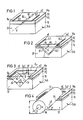
Die Erfindung wird anhand der Figuren in der nachfolgenden Beschreibung eines bevorzugten Ausführungsbeispiels näher erläutert. Von den Figuren zeigen:
- Figur 1 ein Substrat mit einem planar integrierten Wellenleiter und einer auf der Oberfläche des Substrats aufgebrachten Ätzmaske mit zwei parallel zu dem Wellenleiter verlaufenden Schlitzen, die sich von einer Seitenkante des Substrats bis zumindest in Höhe eines für den Wellenleiter vorgesehenen Koppelfensters erstrecken und die als Ausgangsstufe für das Verfahren zur Herstellung einer beispielhaften Vorrichtung dienen,
- Figur 2 die Vorrichtung nach Figur 1 nach dem Ätzen von schlitzförmigen Kanälen, die ausgehend von den Schlitzen der Ätzmaske schräg in die Tiefe des Substrats bis zum Aufeinandertreffen unter dem Koppelfenster führen und zwischen denen eine freitragende Zunge ausgebildet ist, die einen von der Seitenkante des Substrats bis mindestens zum Koppelfenster sich erstreckenden Teil des Wellenleiters enthält,
- Figur 3 das Substrat nach Figur 2 nach Entfernen der freitragenden Zunge bis zum vorgesehenen Koppelfenster, wobei in der Oberfläche des Substrats eine Nut mit V-förmigem Profil ausgebildet ist, die ein offenes Ende und ein durch eine dreieckförmige Fläche des Substrats abgeschlossenes Ende aufweist, in der das Koppelfenster ausgebildet ist, und
- Figur 4 die fertige beispielhafte Anordnung nach Befestigen eines Endabschnitts einer Faser in der Nut so, daß eine Endfläche dieses Endabschnitts, genauer eines Kerns dieses Endabschnitts, gegenüber dem Koppelfenster angeordnet ist und dadurch eine optische Welle zwischen der Faser und dem Wellenleiter überkoppeln kann.
- 1 shows a substrate with a planar integrated waveguide and an etching mask applied to the surface of the substrate with two slots running parallel to the waveguide, which extend from a side edge of the substrate to at least the level of a coupling window provided for the waveguide and which serve as an output stage for the method is used to manufacture an exemplary device,
- 2 shows the device according to FIG. 1 after the etching of slot-shaped channels which, starting from the slots of the etching mask, lead obliquely into the depth of the substrate until they meet under the coupling window and between which a cantilevered tongue is formed, one from the side edge of the substrate contains part of the waveguide extending at least to the coupling window,
- 3 shows the substrate according to FIG. 2 after removal of the self-supporting tongue up to the provided coupling window, a groove having a V-shaped profile being formed in the surface of the substrate and having an open end and an end closed by a triangular surface of the substrate, in FIG the coupling window is formed, and
- Figure 4 shows the finished exemplary arrangement after securing an end portion of a fiber in the groove so that an end face of this end section, more precisely a core of this end section, is arranged opposite the coupling window and can thereby couple an optical wave between the fiber and the waveguide.
In der in Figur 1 dargestellten Ausgangsstufe für das Verfahren zur Herstellung der beispielhaften Anordnung besteht das den planar integrierten Wellenleiter WL tragende Substrat Sub, beispielsweise aus einem Trägerkörper TK aus InP, auf den epitaktisch eine Pufferschicht PS aus InP und darauf eine Deckschicht DS aus InP aufgebracht sind und bei dem der Wellenleiter WL aus einem auf der Pufferschicht PS epitaktisch aufgebrachten, von der Deckschicht umgebenen und von einer mit der Oberfläche O des Substrats eine Seitenkante Ka definierenden Seitenfläche SF des Substrats Sub entlang einer Längsachse A sich in das Innere des Substrats Sub erstreckenden Streifen aus quaternärem Material, beispielsweise InGaAsP-Material besteht. Der Wellenleiter kann beispielsweise die wellenleitende, lichtverstärkende Schicht einer Laserdiode sein.In the output stage shown in FIG. 1 for the method for producing the exemplary arrangement, the substrate Sub carrying the planar integrated waveguide WL consists, for example, of a carrier body TK made of InP, onto which a buffer layer PS made of InP and a covering layer DS made of InP are applied epitaxially and in which the waveguide WL consists of a side surface SF of the substrate Sub which is epitaxially applied to the buffer layer PS, is surrounded by the cover layer and has a side surface Ka which defines a side edge Ka with the surface O of the substrate and extends along a longitudinal axis A into the interior of the substrate Sub Stripe made of quaternary material, such as InGaAsP material. The waveguide can be, for example, the wave-guiding, light-amplifying layer of a laser diode.
Auf die Deckschicht DS ist eine Ätzmaske Ma aufgebracht, in der zwei zu beiden Seiten des planaren Wellenleiters WL angeordnete, parallel zur Längsachse A dieses Wellenleiters WL verlaufende und sich zumindest von der Seitenkante Ka des Substrats bis in Höhe des Koppelfensters KF sich erstreckende längliche Schlitze S11 und S12 ausgespart sind, in denen die Oberfläche O des Substrat freiliegt. Die Höhe der Koppelfläche KF entspricht dem in Richtung der Achse A gemessenen Abstand des Koppelfensters KF von der Seitenkante Ka des Substrats Sub.An etching mask Ma is applied to the cover layer DS, in which two elongated slots S11 are arranged on both sides of the planar waveguide WL, parallel to the longitudinal axis A of this waveguide WL and extending at least from the side edge Ka of the substrate to the level of the coupling window KF and S12 are recessed in which the surface O of the substrate is exposed. The height of the coupling surface KF corresponds to the distance of the coupling window KF from the side edge Ka of the substrate Sub measured in the direction of the axis A.
Die Schlitze S11 und S12 können in einem bekannten photolithographischen Prozeß hergestellt werden.The slots S11 and S12 can be made in a known photolithographic process.
Ausgehend von den Schlitzen S11 und S12 werden schräg in die Tiefe aufeinander zu Schlitzförmige Kanäle K11 und K12 in das Substrat geätzt, bis sie in der Tiefe des Substrats Sub unter dem Wellenleiter WL aufeinandertreffen oder sich kreuzen (Figur 2). Diese schlitzförmgien Kanäle K11 und K12 liegen in zwei sich kreuzenden Ebenen, wobei die nicht dargestellte und im Substrat verlaufende Schnittlinie unter dem Wellenleiter WL und parallel zur Achse A des Wellenleiters WL verläuft.Starting from the slots S11 and S12, slit-shaped channels K11 and K12 are slanted into one another in depth Etched substrate until they meet or intersect in the depth of the substrate Sub under the waveguide WL (Figure 2). These slot-shaped channels K11 and K12 lie in two intersecting planes, the cutting line (not shown) running in the substrate running below the waveguide WL and parallel to the axis A of the waveguide WL.
Zwischen den beiden schlitzförmigen Kanälen K11 und K12 befindet sich eine freitragende Zunge Z mit dreieckförmigem Querschnitt, die sich von der Seitenkante Ka des Substrats Sub in Richtung der Achse A des Wellenleiters WL bis zu den Enden e1 und e2 der Schlitze S11 bzs. S12 der Maske Ma erstreckt.Between the two slot-shaped channels K11 and K12 there is a self-supporting tongue Z with a triangular cross-section, which extends from the side edge Ka of the substrate Sub in the direction of the axis A of the waveguide WL to the ends e1 and e2 of the slots S11 and. S12 of the mask Ma extends.
Als Ätzverfahren kann laserinduzierte Naßätzen verwendet werden (siehe dazu beispielsweise Appl. Phys. Lett. 46 (1985) S. 453-455).Laser-induced wet etching can be used as the etching method (see, for example, Appl. Phys. Lett. 46 (1985) pp. 453-455).
Die Zunge Z wird bis zum Koppelfenster KF entfernt (Figur 3). Dies kann durch Abspalten der frei tragenden Zunge in einem Ultraschallbad erfolgen.The tongue Z is removed up to the coupling window KF (FIG. 3). This can be done by splitting off the cantilevered tongue in an ultrasonic bath.
Nach dem Entfernen der freitragenden Zunge Z entsteht eine in Richtung der Achse A des Wellenleiters WL verlaufende Nut FK an der Oberfläche O des Substrats Sub mit dreieckförmigem Querschnitt, die an der Seitenkante Ka des Substrats Sub ein offenes Ende oE und ein durch eine im wesentlichen vertikal zur Längsachse A stehende, dreieckförmige Substratfläche SuF abgeschlossenes Ende aE aufweist, in welcher das Koppelfenster KF in Form eines gegenüber der Seitenfläche SF des Substrats zurückversetzten, freigelegten Endes des Wellenleiters WL angeordnet ist.After removal of the cantilevered tongue Z, a groove FK running in the direction of the axis A of the waveguide WL is formed on the surface O of the substrate Sub with a triangular cross section, that on the side edge Ka of the substrate Sub has an open end oE and a through a substantially vertical Triangular substrate surface SuF standing at the longitudinal axis A has an end aE in which the coupling window KF is arranged in the form of an exposed end of the waveguide WL set back from the side surface SF of the substrate.
Die Lage des Koppelfensters KF braucht durch die Enden e1 und e2 der Schlitze S11 und S12 der Ätzmaske Ma nur in etwa festgelegt werden und ist unkritisch. In der Praxis wird das Koppelfenster KF etwas näher an der Seitenkante Ka des Substrats Sub liegen als die genannten Enden e1 und e2.The position of the coupling window KF only needs to be approximately determined by the ends e1 and e2 of the slots S11 and S12 of the etching mask Ma and is not critical. In practice, the coupling window KF will be somewhat closer to the side edge Ka of the substrate Sub than the ends e1 and e2 mentioned.
In der Nut FK kann bei geeigneter Dimensionierung ein Endabschnitt EF einer Glasfaser, beispielsweise einer Kern-Mantel-Glasfaser mit einem Kern K und einem Mantel M so befestigt werden, daß das Ende FE dieses Endabschnitts EF, genauer des Kerns dieses Endabschnitts, gegenüber dem Koppelfenster KF des Wellenleiters WL liegt und der Endabschnitt EF und der Wellenleiter WL fluchten (Figur 4).With suitable dimensioning, an end section EF of a glass fiber, for example a core-cladding glass fiber with a core K and a cladding M, can be fastened in the groove FK in such a way that the end FE of this end section EF, more precisely the core of this end section, opposite the coupling window KF of the waveguide WL lies and the end section EF and the waveguide WL are aligned (FIG. 4).
Zur besseren Modenanpassung kann das Ende FE des Endabschnitts EF als Taper mit angeschlossener Linse ausgebildet sein.For better mode adaptation, the end FE of the end section EF can be designed as a taper with a connected lens.
Bei einer Flankenneigung α = 45° der Nut FK und einem äußeren Manteldurchmesser d der Faser muß die Breite D der Nut an der Oberfläche O des Substrats Sub gleich D = √2.d+2a sein, damit die Achse des zur Längsachse A konzentrisch angenommenen Faserkerns K im Abstand a unter der Oberfläche O des Substrats Sub den integrierten Wellenleiter WL trifft.With a slope α = 45 ° of the groove FK and an outer jacket diameter d of the fiber, the width D of the groove on the surface O of the substrate Sub must be D = √2.d + 2a so that the axis of the axis is assumed to be concentric with the longitudinal axis A. Fiber core K at a distance a below the surface O of the substrate Sub meets the integrated waveguide WL.
Bei mehreren anzukoppelnden Fasern erlaubt der geringe Platzbedarf minimalen lateralen Abstand der einzelnen Koppelfenster oder -stellen voneinander. Das Verfahren ist geeignet für Anwendungen, bei denen die photolithographisch und ätztechnisch erreichbaren Toleranzen ausreichen, um die Faser mit nur geringer oder sogar ohne Justage innerhalb der Nut mit V-förmigem Querschnitt relativ zum Koppelfenster bzw. zur Koppelstelle hinreichend genau zu positionieren.If there are several fibers to be coupled, the small space requirement allows a minimal lateral distance between the individual coupling windows or points. The method is suitable for applications in which the tolerances that can be achieved by photolithography and etching are sufficient to position the fiber with sufficient little or no adjustment within the groove with a V-shaped cross section relative to the coupling window or the coupling point.
Bei einem Ausführungsbeispiel wurde eine etwa 50 µm breite Zunge Z durch laserinduziertes Naßätzen erzeugt, wobei als Ätzmaske eine aufgedampfte Titanschicht verwendet wurde.In one exemplary embodiment, an approximately 50 μm wide tongue Z was produced by laser-induced wet etching, an evaporated titanium layer being used as the etching mask.
Die Nuten zum Befestigen der Faserendabschnitte müssen nicht an einem Ende offen sein. Sie können an jeder beliebigen Stelle der Oberfläche des Substrats hergestellt werden und an beiden Enden durch Substratflächen abgeschlossen sein. Die Ankopplung einer parallel an die Oberfläche des Substrats herangeführten Faser ist in diesem Falle möglich, wenn die Länge der Nut ausreicht, um die Faser durch Krümmung an einem abgeschlossenen Ende der Nut aus der Oberfläche des Substrast herauszuführen.The grooves for attaching the fiber end portions need not be open at one end. They can be produced at any point on the surface of the substrate and can be closed off at both ends by substrate surfaces. In this case, it is possible to couple a fiber that is guided parallel to the surface of the substrate if the length of the groove is sufficient to bend the fiber around a fiber lead the completed end of the groove out of the surface of the substrate.
Claims (3)
Applications Claiming Priority (2)
| Application Number | Priority Date | Filing Date | Title |
|---|---|---|---|
| DE3833147 | 1988-09-29 | ||
| DE3833147 | 1988-09-29 |
Publications (2)
| Publication Number | Publication Date |
|---|---|
| EP0361153A2 true EP0361153A2 (en) | 1990-04-04 |
| EP0361153A3 EP0361153A3 (en) | 1991-07-24 |
Family
ID=6364022
Family Applications (1)
| Application Number | Title | Priority Date | Filing Date |
|---|---|---|---|
| EP19890116456 Ceased EP0361153A3 (en) | 1988-09-29 | 1989-09-06 | Arrangement for coupling an optical fibre with a coupling window of a planar integrated optical device, and method for making such an arrangement |
Country Status (3)
| Country | Link |
|---|---|
| US (1) | US4973133A (en) |
| EP (1) | EP0361153A3 (en) |
| JP (1) | JPH031112A (en) |
Cited By (8)
| Publication number | Priority date | Publication date | Assignee | Title |
|---|---|---|---|---|
| WO1992009912A1 (en) * | 1990-11-30 | 1992-06-11 | United Technologies Corporation | Pigtailing optical fiber |
| FR2707401A1 (en) * | 1993-07-09 | 1995-01-13 | Menigaux Louis | A method of manufacturing a structure incorporating a cleaved optical guide to an optical fiber support for optical fiber-guide coupling and structure obtained. |
| WO1995004296A1 (en) * | 1993-07-27 | 1995-02-09 | Siemens Aktiengesellschaft | Process and device for manufacturing a silicon semiconductor substrate with an integrated waveguide coupled to an optical fibre |
| EP0670084A4 (en) * | 1992-11-17 | 1995-06-28 | Gte Laboratories Inc | A monolithically integrated semiconductor structure and method of fabricating such structure. |
| US5570385A (en) * | 1991-11-07 | 1996-10-29 | Goldstar Co., Ltd. | Semiconductor laser and method for manufacturing the same |
| US5579424A (en) * | 1993-06-18 | 1996-11-26 | Siemens Aktiengesellschaft | Arrangement for an optical coupling of a fiber to a planar optical waveguide and a method of forming the arrangement |
| US6090635A (en) * | 1992-11-17 | 2000-07-18 | Gte Laboratories Incorporated | Method for forming a semiconductor device structure having a laser portion |
| WO2002021184A1 (en) * | 2000-09-11 | 2002-03-14 | Fci | Monolithic semiconductor photo-coupler incorporating an optical fiber alignment groove |
Families Citing this family (20)
| Publication number | Priority date | Publication date | Assignee | Title |
|---|---|---|---|---|
| US4741796A (en) * | 1985-05-29 | 1988-05-03 | Siemens Aktiengesellschaft | Method for positioning and bonding a solid body to a support base |
| DE58904033D1 (en) * | 1988-02-19 | 1993-05-19 | Siemens Ag | INSULATING DEVICE FOR OPTICALLY INSULATING INTEGRATED COMPONENTS. |
| GB8805015D0 (en) * | 1988-03-02 | 1988-03-30 | British Telecomm | Optical fibre locating apparatus |
| EP0419767B1 (en) * | 1989-09-29 | 1993-11-24 | Siemens Aktiengesellschaft | Method for manufacturing a Silicon body |
| US5077818A (en) * | 1989-09-29 | 1991-12-31 | Siemens Aktiengesellschaft | Coupling arrangement for optically coupling a fiber to a planar optical waveguide integrated on a substrate |
| US5046809A (en) * | 1989-09-29 | 1991-09-10 | Siemens Aktiengesellschaft | Coupling arrangement for optically coupling a fiber to a planar optical waveguide integrated on a substrate |
| FR2659148B1 (en) * | 1990-03-01 | 1993-04-16 | Commissariat Energie Atomique | METHOD FOR CONNECTING BETWEEN AN OPTICAL FIBER AND AN OPTICAL MICROGUIDE. |
| GB9021944D0 (en) * | 1990-10-09 | 1990-11-21 | British Telecomm | Self-aligned-v-groves and waveguides |
| US5080458A (en) * | 1990-10-22 | 1992-01-14 | United Technologies Corporation | Method and apparatus for positioning an optical fiber |
| JP2839699B2 (en) * | 1990-11-08 | 1998-12-16 | 株式会社東芝 | Traveling wave optical amplifier |
| US5175781A (en) * | 1991-10-11 | 1992-12-29 | United Technologies Corporation | Attaching optical fibers to integrated optic chips |
| US5217568A (en) * | 1992-02-03 | 1993-06-08 | Motorola, Inc. | Silicon etching process using polymeric mask, for example, to form V-groove for an optical fiber coupling |
| US5379359A (en) * | 1992-09-29 | 1995-01-03 | Eastman Kodak Company | Laser diode coupling to waveguide and method of making same using substrate etching |
| US5357593A (en) * | 1993-10-12 | 1994-10-18 | Alliedsignal Inc. | Method of attaching optical fibers to opto-electronic integrated circuits on silicon substrates |
| GB2297626A (en) * | 1995-01-27 | 1996-08-07 | Cambridge Consultants | Miniature mounting grooved substrate |
| WO1997042534A1 (en) * | 1996-05-03 | 1997-11-13 | Bookham Technology Limited | Connection between an integrated optical waveguide and an optical fibre |
| US6913399B2 (en) * | 2003-07-23 | 2005-07-05 | Intel Corporation | Metallized optical fibers and ferrules for optical fibers for direct attachment to photodiodes |
| US7494598B2 (en) * | 2005-11-22 | 2009-02-24 | Honeywell International Inc. | Miniature optically transparent window |
| KR100868848B1 (en) * | 2006-03-06 | 2008-11-14 | 주식회사 엘지화학 | Metallic laminate and method for preparing the same |
| DE102008051625B4 (en) * | 2008-10-02 | 2015-08-13 | Erich Kasper | Method for producing a component with an optical coupling window |
Citations (4)
| Publication number | Priority date | Publication date | Assignee | Title |
|---|---|---|---|---|
| JPS57143890A (en) * | 1981-03-02 | 1982-09-06 | Fujitsu Ltd | Semiconductor laser device and its manufacture |
| US4466696A (en) * | 1982-03-29 | 1984-08-21 | Honeywell Inc. | Self-aligned coupling of optical fiber to semiconductor laser or LED |
| JPS59193083A (en) * | 1983-04-15 | 1984-11-01 | Hitachi Ltd | Semiconductor laser device for fiber loading |
| JPS59197184A (en) * | 1983-04-25 | 1984-11-08 | Nec Corp | Semiconductor laser |
Family Cites Families (8)
| Publication number | Priority date | Publication date | Assignee | Title |
|---|---|---|---|---|
| US4301462A (en) * | 1978-08-03 | 1981-11-17 | Westinghouse Electric Corp. | Light activated silicon switch with etched channel in cathode base and anode emitter communicating with cladded optical fiber |
| FR2574950B1 (en) * | 1984-12-18 | 1987-09-25 | Corning Glass Works | GLASS INTEGRATED OPTICAL COMPONENTS AND THEIR MANUFACTURE |
| JPS6217711A (en) * | 1985-07-16 | 1987-01-26 | Matsushita Electric Ind Co Ltd | Coupling method for optical fiber and distribution refractive index type waveguide |
| EP0223414B1 (en) * | 1985-10-16 | 1994-01-12 | BRITISH TELECOMMUNICATIONS public limited company | Mounting a component to a substrate |
| US4759595A (en) * | 1986-03-25 | 1988-07-26 | Apa Optics, Inc. | Integrated optic switch |
| JPS63223716A (en) * | 1987-03-13 | 1988-09-19 | Seiko Instr & Electronics Ltd | Optical coupling device |
| US4826272A (en) * | 1987-08-27 | 1989-05-02 | American Telephone And Telegraph Company At&T Bell Laboratories | Means for coupling an optical fiber to an opto-electronic device |
| US4883743A (en) * | 1988-01-15 | 1989-11-28 | E. I. Du Pont De Nemours And Company | Optical fiber connector assemblies and methods of making the assemblies |
-
1989
- 1989-09-06 EP EP19890116456 patent/EP0361153A3/en not_active Ceased
- 1989-09-13 US US07/406,599 patent/US4973133A/en not_active Expired - Fee Related
- 1989-09-27 JP JP1253720A patent/JPH031112A/en active Pending
Patent Citations (4)
| Publication number | Priority date | Publication date | Assignee | Title |
|---|---|---|---|---|
| JPS57143890A (en) * | 1981-03-02 | 1982-09-06 | Fujitsu Ltd | Semiconductor laser device and its manufacture |
| US4466696A (en) * | 1982-03-29 | 1984-08-21 | Honeywell Inc. | Self-aligned coupling of optical fiber to semiconductor laser or LED |
| JPS59193083A (en) * | 1983-04-15 | 1984-11-01 | Hitachi Ltd | Semiconductor laser device for fiber loading |
| JPS59197184A (en) * | 1983-04-25 | 1984-11-08 | Nec Corp | Semiconductor laser |
Non-Patent Citations (3)
| Title |
|---|
| PATENT ABSTRACTS OF JAPAN, Band 6, Nr. 243 (E-145)[1121], 2. Dezember 1982; & JP-A-57 143 890 (FUJITSU) 06-09-1982 * |
| PATENT ABSTRACTS OF JAPAN, Band 9, Nr. 53 (E-301)[1776], 7. März 1985; & JP-A-59 193 083 (HITACHI) 01-11-1984 * |
| PATENT ABSTRACTS OF JAPAN, Band 9, Nr. 56 (E-302)[1779], 12. März 1985; & JP-A-59 197 184 (NIPPON DENKI) 08-11-1984 * |
Cited By (12)
| Publication number | Priority date | Publication date | Assignee | Title |
|---|---|---|---|---|
| WO1992009912A1 (en) * | 1990-11-30 | 1992-06-11 | United Technologies Corporation | Pigtailing optical fiber |
| US5570385A (en) * | 1991-11-07 | 1996-10-29 | Goldstar Co., Ltd. | Semiconductor laser and method for manufacturing the same |
| EP0670084A4 (en) * | 1992-11-17 | 1995-06-28 | Gte Laboratories Inc | A monolithically integrated semiconductor structure and method of fabricating such structure. |
| EP0670084A1 (en) * | 1992-11-17 | 1995-09-06 | Gte Laboratories Incorporated | A monolithically integrated semiconductor structure and method of fabricating such structure |
| US6090635A (en) * | 1992-11-17 | 2000-07-18 | Gte Laboratories Incorporated | Method for forming a semiconductor device structure having a laser portion |
| US5579424A (en) * | 1993-06-18 | 1996-11-26 | Siemens Aktiengesellschaft | Arrangement for an optical coupling of a fiber to a planar optical waveguide and a method of forming the arrangement |
| FR2707401A1 (en) * | 1993-07-09 | 1995-01-13 | Menigaux Louis | A method of manufacturing a structure incorporating a cleaved optical guide to an optical fiber support for optical fiber-guide coupling and structure obtained. |
| EP0637764A1 (en) * | 1993-07-09 | 1995-02-08 | France Telecom | Fabrication of an optical coupling structure, which integrates a cleaved optical waveguide and a support for an optical fiber |
| US5518965A (en) * | 1993-07-09 | 1996-05-21 | France Telecom | Process for producing a structure integrating a cleaved optical guide with an optical fibre support for a guide-fibre optical coupling |
| WO1995004296A1 (en) * | 1993-07-27 | 1995-02-09 | Siemens Aktiengesellschaft | Process and device for manufacturing a silicon semiconductor substrate with an integrated waveguide coupled to an optical fibre |
| US5700382A (en) * | 1993-07-27 | 1997-12-23 | Siemens Aktiengesellschaft | Method for fabricating a silicon semiconductor substrate having an integrated waveguide and an optical fiber coupled thereto |
| WO2002021184A1 (en) * | 2000-09-11 | 2002-03-14 | Fci | Monolithic semiconductor photo-coupler incorporating an optical fiber alignment groove |
Also Published As
| Publication number | Publication date |
|---|---|
| JPH031112A (en) | 1991-01-07 |
| EP0361153A3 (en) | 1991-07-24 |
| US4973133A (en) | 1990-11-27 |
Similar Documents
| Publication | Publication Date | Title |
|---|---|---|
| EP0361153A2 (en) | Arrangement for coupling an optical fibre with a coupling window of a planar integrated optical device, and method for making such an arrangement | |
| DE69837236T2 (en) | OPTICAL MODULE | |
| EP0498170B1 (en) | Integrated optical component for coupling waveguides of different dimensions | |
| DE2750322C3 (en) | Optical device for coupling the radiation emerging from a semiconductor laser into an optical fiber | |
| EP0187198A2 (en) | Method of manufacturing an integrated optical device | |
| DE19917596B4 (en) | Bidirectional optical communication device and bidirectional optical communication device | |
| EP0583679A1 (en) | Device to change an optical wave with a relatively small cross section to an optical wave with a relatively large cross section | |
| EP0155379A2 (en) | Arrangement for coupling a light wave guide to a semiconductor laser and method for manufacturing such an arrangement | |
| EP0495202B1 (en) | Device to change an optical wave with a small waist diameter into a wave with a bigger waist diameter | |
| DE2744128A1 (en) | WAVE GUIDE WITH A LATERAL DETECTOR | |
| EP0267536A2 (en) | Hermetically sealed connecting passage for glass fibre | |
| DE19626113A1 (en) | Optical semiconductor component with a deep ribbed waveguide | |
| DE2331497A1 (en) | ARRANGEMENT FOR COUPLING LASER BEAMS INTO OPTICAL FIBERS | |
| EP0589902B1 (en) | Integrated optical circuit | |
| DE3829540C2 (en) | Bent waveguide for an integrated optical circuit | |
| DE4313492C1 (en) | Optical coupler for laser monitoring diode, esp. for semiconductor laser | |
| EP0948752B1 (en) | Optoelectronic module | |
| DE3601729A1 (en) | Fibre-optic coupling arrangement | |
| DE2446152C3 (en) | Adjustable coupling arrangement for connecting and aligning at least two optical waveguides of an optical communication system on a common optical axis | |
| DE4312263B4 (en) | Method for picking up a light signal | |
| DE60201464T2 (en) | Semiconductor laser | |
| EP0737872A2 (en) | Optical branching element | |
| DE60312766T2 (en) | Optical coupling device and its manufacturing method | |
| EP0744798A1 (en) | Device for laser coupling | |
| DE19827553A1 (en) | Optic coupling element for optical sensors and communication systems |
Legal Events
| Date | Code | Title | Description |
|---|---|---|---|
| PUAI | Public reference made under article 153(3) epc to a published international application that has entered the european phase |
Free format text: ORIGINAL CODE: 0009012 |
|
| AK | Designated contracting states |
Kind code of ref document: A2 Designated state(s): DE FR GB IT NL SE |
|
| 17P | Request for examination filed |
Effective date: 19901205 |
|
| PUAL | Search report despatched |
Free format text: ORIGINAL CODE: 0009013 |
|
| AK | Designated contracting states |
Kind code of ref document: A3 Designated state(s): DE FR GB IT NL SE |
|
| 17Q | First examination report despatched |
Effective date: 19940215 |
|
| STAA | Information on the status of an ep patent application or granted ep patent |
Free format text: STATUS: THE APPLICATION HAS BEEN REFUSED |
|
| 18R | Application refused |
Effective date: 19950916 |