EP0361195A2 - Printed circuit board with moulded substrate - Google Patents
Printed circuit board with moulded substrate Download PDFInfo
- Publication number
- EP0361195A2 EP0361195A2 EP19890116804 EP89116804A EP0361195A2 EP 0361195 A2 EP0361195 A2 EP 0361195A2 EP 19890116804 EP19890116804 EP 19890116804 EP 89116804 A EP89116804 A EP 89116804A EP 0361195 A2 EP0361195 A2 EP 0361195A2
- Authority
- EP
- European Patent Office
- Prior art keywords
- depressions
- substrate
- trench
- metal coating
- printed circuit
- Prior art date
- Legal status (The legal status is an assumption and is not a legal conclusion. Google has not performed a legal analysis and makes no representation as to the accuracy of the status listed.)
- Granted
Links
Images

Classifications
-
- H—ELECTRICITY
- H05—ELECTRIC TECHNIQUES NOT OTHERWISE PROVIDED FOR
- H05K—PRINTED CIRCUITS; CASINGS OR CONSTRUCTIONAL DETAILS OF ELECTRIC APPARATUS; MANUFACTURE OF ASSEMBLAGES OF ELECTRICAL COMPONENTS
- H05K1/00—Printed circuits
- H05K1/02—Details
- H05K1/11—Printed elements for providing electric connections to or between printed circuits
- H05K1/115—Via connections; Lands around holes or via connections
- H05K1/116—Lands, clearance holes or other lay-out details concerning the surrounding of a via
-
- H—ELECTRICITY
- H05—ELECTRIC TECHNIQUES NOT OTHERWISE PROVIDED FOR
- H05K—PRINTED CIRCUITS; CASINGS OR CONSTRUCTIONAL DETAILS OF ELECTRIC APPARATUS; MANUFACTURE OF ASSEMBLAGES OF ELECTRICAL COMPONENTS
- H05K1/00—Printed circuits
-
- H—ELECTRICITY
- H05—ELECTRIC TECHNIQUES NOT OTHERWISE PROVIDED FOR
- H05K—PRINTED CIRCUITS; CASINGS OR CONSTRUCTIONAL DETAILS OF ELECTRIC APPARATUS; MANUFACTURE OF ASSEMBLAGES OF ELECTRICAL COMPONENTS
- H05K3/00—Apparatus or processes for manufacturing printed circuits
- H05K3/10—Apparatus or processes for manufacturing printed circuits in which conductive material is applied to the insulating support in such a manner as to form the desired conductive pattern
- H05K3/107—Apparatus or processes for manufacturing printed circuits in which conductive material is applied to the insulating support in such a manner as to form the desired conductive pattern by filling grooves in the support with conductive material
-
- H—ELECTRICITY
- H05—ELECTRIC TECHNIQUES NOT OTHERWISE PROVIDED FOR
- H05K—PRINTED CIRCUITS; CASINGS OR CONSTRUCTIONAL DETAILS OF ELECTRIC APPARATUS; MANUFACTURE OF ASSEMBLAGES OF ELECTRICAL COMPONENTS
- H05K2201/00—Indexing scheme relating to printed circuits covered by H05K1/00
- H05K2201/03—Conductive materials
- H05K2201/0332—Structure of the conductor
- H05K2201/0364—Conductor shape
- H05K2201/0376—Flush conductors, i.e. flush with the surface of the printed circuit
-
- H—ELECTRICITY
- H05—ELECTRIC TECHNIQUES NOT OTHERWISE PROVIDED FOR
- H05K—PRINTED CIRCUITS; CASINGS OR CONSTRUCTIONAL DETAILS OF ELECTRIC APPARATUS; MANUFACTURE OF ASSEMBLAGES OF ELECTRICAL COMPONENTS
- H05K2201/00—Indexing scheme relating to printed circuits covered by H05K1/00
- H05K2201/09—Shape and layout
- H05K2201/09009—Substrate related
- H05K2201/09036—Recesses or grooves in insulating substrate
-
- H—ELECTRICITY
- H05—ELECTRIC TECHNIQUES NOT OTHERWISE PROVIDED FOR
- H05K—PRINTED CIRCUITS; CASINGS OR CONSTRUCTIONAL DETAILS OF ELECTRIC APPARATUS; MANUFACTURE OF ASSEMBLAGES OF ELECTRICAL COMPONENTS
- H05K2201/00—Indexing scheme relating to printed circuits covered by H05K1/00
- H05K2201/09—Shape and layout
- H05K2201/09009—Substrate related
- H05K2201/09118—Moulded substrate
-
- H—ELECTRICITY
- H05—ELECTRIC TECHNIQUES NOT OTHERWISE PROVIDED FOR
- H05K—PRINTED CIRCUITS; CASINGS OR CONSTRUCTIONAL DETAILS OF ELECTRIC APPARATUS; MANUFACTURE OF ASSEMBLAGES OF ELECTRICAL COMPONENTS
- H05K2201/00—Indexing scheme relating to printed circuits covered by H05K1/00
- H05K2201/09—Shape and layout
- H05K2201/09818—Shape or layout details not covered by a single group of H05K2201/09009 - H05K2201/09809
- H05K2201/09827—Tapered, e.g. tapered hole, via or groove
-
- H—ELECTRICITY
- H05—ELECTRIC TECHNIQUES NOT OTHERWISE PROVIDED FOR
- H05K—PRINTED CIRCUITS; CASINGS OR CONSTRUCTIONAL DETAILS OF ELECTRIC APPARATUS; MANUFACTURE OF ASSEMBLAGES OF ELECTRICAL COMPONENTS
- H05K2201/00—Indexing scheme relating to printed circuits covered by H05K1/00
- H05K2201/09—Shape and layout
- H05K2201/09818—Shape or layout details not covered by a single group of H05K2201/09009 - H05K2201/09809
- H05K2201/09845—Stepped hole, via, edge, bump or conductor
-
- H—ELECTRICITY
- H05—ELECTRIC TECHNIQUES NOT OTHERWISE PROVIDED FOR
- H05K—PRINTED CIRCUITS; CASINGS OR CONSTRUCTIONAL DETAILS OF ELECTRIC APPARATUS; MANUFACTURE OF ASSEMBLAGES OF ELECTRICAL COMPONENTS
- H05K2201/00—Indexing scheme relating to printed circuits covered by H05K1/00
- H05K2201/09—Shape and layout
- H05K2201/09818—Shape or layout details not covered by a single group of H05K2201/09009 - H05K2201/09809
- H05K2201/09981—Metallised walls
-
- H—ELECTRICITY
- H05—ELECTRIC TECHNIQUES NOT OTHERWISE PROVIDED FOR
- H05K—PRINTED CIRCUITS; CASINGS OR CONSTRUCTIONAL DETAILS OF ELECTRIC APPARATUS; MANUFACTURE OF ASSEMBLAGES OF ELECTRICAL COMPONENTS
- H05K2203/00—Indexing scheme relating to apparatus or processes for manufacturing printed circuits covered by H05K3/00
- H05K2203/05—Patterning and lithography; Masks; Details of resist
- H05K2203/0562—Details of resist
- H05K2203/0574—Stacked resist layers used for different processes
-
- H—ELECTRICITY
- H05—ELECTRIC TECHNIQUES NOT OTHERWISE PROVIDED FOR
- H05K—PRINTED CIRCUITS; CASINGS OR CONSTRUCTIONAL DETAILS OF ELECTRIC APPARATUS; MANUFACTURE OF ASSEMBLAGES OF ELECTRICAL COMPONENTS
- H05K2203/00—Indexing scheme relating to apparatus or processes for manufacturing printed circuits covered by H05K3/00
- H05K2203/14—Related to the order of processing steps
- H05K2203/1415—Applying catalyst after applying plating resist
-
- H—ELECTRICITY
- H05—ELECTRIC TECHNIQUES NOT OTHERWISE PROVIDED FOR
- H05K—PRINTED CIRCUITS; CASINGS OR CONSTRUCTIONAL DETAILS OF ELECTRIC APPARATUS; MANUFACTURE OF ASSEMBLAGES OF ELECTRICAL COMPONENTS
- H05K3/00—Apparatus or processes for manufacturing printed circuits
- H05K3/10—Apparatus or processes for manufacturing printed circuits in which conductive material is applied to the insulating support in such a manner as to form the desired conductive pattern
- H05K3/18—Apparatus or processes for manufacturing printed circuits in which conductive material is applied to the insulating support in such a manner as to form the desired conductive pattern using precipitation techniques to apply the conductive material
- H05K3/181—Apparatus or processes for manufacturing printed circuits in which conductive material is applied to the insulating support in such a manner as to form the desired conductive pattern using precipitation techniques to apply the conductive material by electroless plating
- H05K3/182—Apparatus or processes for manufacturing printed circuits in which conductive material is applied to the insulating support in such a manner as to form the desired conductive pattern using precipitation techniques to apply the conductive material by electroless plating characterised by the patterning method
- H05K3/184—Apparatus or processes for manufacturing printed circuits in which conductive material is applied to the insulating support in such a manner as to form the desired conductive pattern using precipitation techniques to apply the conductive material by electroless plating characterised by the patterning method using masks
-
- H—ELECTRICITY
- H05—ELECTRIC TECHNIQUES NOT OTHERWISE PROVIDED FOR
- H05K—PRINTED CIRCUITS; CASINGS OR CONSTRUCTIONAL DETAILS OF ELECTRIC APPARATUS; MANUFACTURE OF ASSEMBLAGES OF ELECTRICAL COMPONENTS
- H05K3/00—Apparatus or processes for manufacturing printed circuits
- H05K3/30—Assembling printed circuits with electric components, e.g. with resistor
- H05K3/32—Assembling printed circuits with electric components, e.g. with resistor electrically connecting electric components or wires to printed circuits
- H05K3/34—Assembling printed circuits with electric components, e.g. with resistor electrically connecting electric components or wires to printed circuits by soldering
- H05K3/3452—Solder masks
-
- H—ELECTRICITY
- H05—ELECTRIC TECHNIQUES NOT OTHERWISE PROVIDED FOR
- H05K—PRINTED CIRCUITS; CASINGS OR CONSTRUCTIONAL DETAILS OF ELECTRIC APPARATUS; MANUFACTURE OF ASSEMBLAGES OF ELECTRICAL COMPONENTS
- H05K3/00—Apparatus or processes for manufacturing printed circuits
- H05K3/40—Forming printed elements for providing electric connections to or between printed circuits
- H05K3/42—Plated through-holes or plated via connections
- H05K3/425—Plated through-holes or plated via connections characterised by the sequence of steps for plating the through-holes or via connections in relation to the conductive pattern
- H05K3/426—Plated through-holes or plated via connections characterised by the sequence of steps for plating the through-holes or via connections in relation to the conductive pattern initial plating of through-holes in substrates without metal
-
- Y—GENERAL TAGGING OF NEW TECHNOLOGICAL DEVELOPMENTS; GENERAL TAGGING OF CROSS-SECTIONAL TECHNOLOGIES SPANNING OVER SEVERAL SECTIONS OF THE IPC; TECHNICAL SUBJECTS COVERED BY FORMER USPC CROSS-REFERENCE ART COLLECTIONS [XRACs] AND DIGESTS
- Y10—TECHNICAL SUBJECTS COVERED BY FORMER USPC
- Y10T—TECHNICAL SUBJECTS COVERED BY FORMER US CLASSIFICATION
- Y10T29/00—Metal working
- Y10T29/49—Method of mechanical manufacture
- Y10T29/49002—Electrical device making
- Y10T29/49117—Conductor or circuit manufacturing
- Y10T29/49124—On flat or curved insulated base, e.g., printed circuit, etc.
- Y10T29/49155—Manufacturing circuit on or in base
- Y10T29/49158—Manufacturing circuit on or in base with molding of insulated base
- Y10T29/4916—Simultaneous circuit manufacturing
-
- Y—GENERAL TAGGING OF NEW TECHNOLOGICAL DEVELOPMENTS; GENERAL TAGGING OF CROSS-SECTIONAL TECHNOLOGIES SPANNING OVER SEVERAL SECTIONS OF THE IPC; TECHNICAL SUBJECTS COVERED BY FORMER USPC CROSS-REFERENCE ART COLLECTIONS [XRACs] AND DIGESTS
- Y10—TECHNICAL SUBJECTS COVERED BY FORMER USPC
- Y10T—TECHNICAL SUBJECTS COVERED BY FORMER US CLASSIFICATION
- Y10T29/00—Metal working
- Y10T29/49—Method of mechanical manufacture
- Y10T29/49002—Electrical device making
- Y10T29/49117—Conductor or circuit manufacturing
- Y10T29/49124—On flat or curved insulated base, e.g., printed circuit, etc.
- Y10T29/49155—Manufacturing circuit on or in base
- Y10T29/49165—Manufacturing circuit on or in base by forming conductive walled aperture in base
Definitions
- the invention relates to a printed circuit board with an injection molded substrate, in the surface of which the circuit pattern is recessed by trench-shaped depressions in the area of conductor tracks and by flat depressions in the area of plated-through holes and / or connection areas and the recessed areas have a conductive metal coating.
- Such printed circuit boards with injection molded or similarly shaped substrates are already known from DE-A-27 15 875 or the corresponding CA-A-10 75 825 or also from US-A-45 32 152.
- the substrate is first formed in a form in which the conductor pattern and via holes are contained in the form of depressions. After a mechanical and / or chemical surface treatment, the substrate is then chemically activated, whereupon the raised surfaces of the substrate are covered with a protective layer. When this protective layer is applied, only the depressions have to be left free, so that complex photostructuring of the resist can be omitted and the application can be carried out, for example, with a doctor blade or by roller coating, the so-called roller coating.
- a conductive metal coating is then preferably applied by electroless metal deposition, which leads to the formation of the entire conductor configuration in the depressions of the substrate and in the via holes.
- a solder resist is applied to the conductor surfaces that are not to be soldered.
- the structuring of the substrate before the metal deposition does not result in photostructuring of the resist is required.
- the application of the solder resist then requires either selective application to the conductor tracks or photo structuring, since the flat depressions which surround the plated-through holes as soldering eyes or which are to serve as connecting surfaces must remain free.
- the invention has for its object to provide a printed circuit board with an injection molded substrate, in which the application of the solder resist can be carried out in a simple manner without photo structuring.
- the invention is based on the knowledge that, due to a geometry of the substrate with correspondingly narrow trench-shaped depressions when electroless or electroless and galvanic deposition of the metal coating, these depressions grow from the bottom and from the side walls until the trench-shaped depression is completely filled. When this complete filling of the trench-shaped depressions is achieved, there is a metal coating in the correspondingly large flat depressions, the thickness of which does not extend to the surface of the substrate and the thickness of which does not fill the flat depressions in the lateral wall area.
- the metal coating is preferably formed by chemically applied copper, which, as already mentioned, is then coated with a suitable solder layer, in particular tin, in the area of soldering eyes, solder pads and through-holes.
- the trench-shaped depressions (30) have an approximately V-shaped cross section. Such a V-shaped cross section then favors the filling of the trench-shaped depressions in the electroless or electroless and galvanic metal deposition.
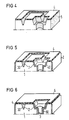
- FIG. 1 shows a section through part of a substrate 1, for example made of glass fiber-reinforced polyetherimide.
- a substrate 1 for example made of glass fiber-reinforced polyetherimide.
- substantially V-shaped trench-shaped depressions 30 of width b, and sheet-like depressions 30 of width B arranged in the region of via holes 60 are already in the injection molding process and in other places sheet-like depressions 50 of the same width B are produced.
- a metal coating 2 the trench-shaped depressions 30 are completely filled with metal up to the surface 10 of the substrate. This is achieved by a correspondingly narrow dimensioning of the width b of the trench-shaped depressions 30, which leads to the growth of the depression 30 during the metal deposition on the bottom and on the side walls of the depression.
- the width B of the flat depressions 40 and 50 is dimensioned in such a way that this overgrowth can in no case occur.
- the metal coating 2 is thus deposited flatly and with a small thickness, so that a distance from the surface 10 of the substrate 1, denoted by A, remains here. This means that even with the same depths of the trench-shaped depressions 30 on the one hand and the flat depressions 40 and 50 on the other hand, a metal deposition carried out in the same bath once extends to the surface 10 of the substrate and ends at a distance A from the surface of the substrate 10.
- the distance A must then be so large in any case that when the surface 10 is coated with a solder resist, only the conductor tracks in the area of the trench-shaped depressions 30 but in no way the soldering eyes in the area of the flat depressions 40 and the connection areas in the area of the flat depressions 50 to be covered.
- a solder resist which cannot be seen from FIG. 1, the areas of the metal layer 2 serving as vias, soldering pads and connection surfaces can be coated with a tin layer 3 by hot tinning.
- a substrate 1 is assumed, which according to the example is an injection molded part FIG. 2 contains the approximately V-shaped trench-shaped depressions 30 corresponding to the conductor pattern, the flat depressions 40 and the vias 60 extending therefrom.
- a coating layer 4 which is a conventional plating resist, is then applied to the surface 10 of this substrate 1 after a conventional surface treatment according to FIG. 3.
- the lacquer layer 4 is applied by roller coating, the depressions 30 and 40 remaining free as a result of the distance A shown in FIG. 1.
- germination 5 is subsequently applied, which is indicated in the drawing by fine dots. This germination 5 is applied, for example, by immersing the substrate 1 in a PdCl2-SnCl2 bath.
- the metal layer 4 is applied to the areas not protected by a lacquer layer 4 by chemical metal deposition without external current. It can be seen that this metal layer 4 applied in a commercially available electroless copper bath has reached a thickness by corresponding dimensioning of the coating duration, which corresponds to a complete filling of the trench-shaped depressions 30 to the substrate surface.
- a solder resist 6 is then applied by roller coating, which leaves the flat depressions 40 and the plated-through holes 60 free and here enables the tin layer 3 to be applied by hot tinning. It can be seen that the lacquer layer 4 does not have to be removed before the solder resist 6 is applied.
Abstract
Description
Die Erfindung betrifft eine Leiterplatte mit einem spritzgegossenen Substrat, in dessen Oberfläche das Leiterbild durch grabenförmige Vertiefungen im Bereich von Leiterbahnen und durch flächige Vertiefungen im Bereich von Durchkontaktierungen und/oder Anschlußflächen ausgespart ist und die ausgesparten Bereiche einen leitenden Metallüberzug aufweisen.The invention relates to a printed circuit board with an injection molded substrate, in the surface of which the circuit pattern is recessed by trench-shaped depressions in the area of conductor tracks and by flat depressions in the area of plated-through holes and / or connection areas and the recessed areas have a conductive metal coating.
Derartige Leiterplatten mit spritzgegossenen oder ähnlich geformten Substraten sind bereits aus der DE-A-27 15 875 bzw. der korrespondierenden CA-A-10 75 825 oder auch aus der US-A-45 32 152 bekannt.Such printed circuit boards with injection molded or similarly shaped substrates are already known from DE-A-27 15 875 or the corresponding CA-A-10 75 825 or also from US-A-45 32 152.
Zur Herstellung der beispielsweise aus der DE-A-27 15 875 bekannten Leiterplatte wird zunächst in einer Form das Substrat gebildet, in welchem das Leiterbild und Durchkontaktierungslöcher in Form von Vertiefungen enthalten sind. Nach einer mechanischen und/oder chemischen Oberflächenbehandlung wird dann das Substrat chemisch aktiviert, worauf die erhabenen Flächen des Substrats mit einer Schutzschicht bedeckt werden. Bei dem Aufbringen dieser Schutzschicht müssen lediglich die Vertiefungen freibleiben, so daß eine aufwendige Fotostrukturierung des Resists entfallen kann und der Auftrag beispielsweise mit einer Rakel oder durch Rollbeschichtung, dem sogenannten Roller-Coating, vorgenommen werden kann. Anschließend wird dann vorzugsweise durch stromlose Metallabscheidung ein leitender Metallüberzug aufgebracht, der in den Vertiefungen des Substrats und in den Durchkontaktierungslöchern zur Bildung der gesamten Leiterkonfiguration führt. Zur Fertigstellung der Leiterplatten wird auf die Leiterflächen, die keine Lötverbindungen eingehen sollen, ein Lötstopplack aufgebracht.To produce the circuit board known, for example, from DE-A-27 15 875, the substrate is first formed in a form in which the conductor pattern and via holes are contained in the form of depressions. After a mechanical and / or chemical surface treatment, the substrate is then chemically activated, whereupon the raised surfaces of the substrate are covered with a protective layer. When this protective layer is applied, only the depressions have to be left free, so that complex photostructuring of the resist can be omitted and the application can be carried out, for example, with a doctor blade or by roller coating, the so-called roller coating. A conductive metal coating is then preferably applied by electroless metal deposition, which leads to the formation of the entire conductor configuration in the depressions of the substrate and in the via holes. To complete the printed circuit boards, a solder resist is applied to the conductor surfaces that are not to be soldered.
Es ist ersichtlich, daß durch die Strukturierung des Substrats vor der Metallabscheidung keine Fotostrukturierung des Resists erforderlich ist. Demgegenüber erfordert dann aber das Aufbringen des Lötstopplacks entweder ein selektives Auftragen auf die Leiterbahnen oder eine Fotostrukturierung, da die flächigen Vertiefungen welche die Durchkontaktierungen als Lötaugen umgeben oder die als Anschlußflächen dienen sollen freibleiben müssen.It can be seen that the structuring of the substrate before the metal deposition does not result in photostructuring of the resist is required. In contrast, the application of the solder resist then requires either selective application to the conductor tracks or photo structuring, since the flat depressions which surround the plated-through holes as soldering eyes or which are to serve as connecting surfaces must remain free.
Der Erfindung liegt die Aufgabe zugrunde, eine Leiterplatte mit einem spritzgegossenen Substrat zu schaffen, bei welcher das Aufbringen des Lötstopplacks ohne Fotostrukturierung auf einfache Weise vorgenommen werden kann.The invention has for its object to provide a printed circuit board with an injection molded substrate, in which the application of the solder resist can be carried out in a simple manner without photo structuring.
Diese Aufgabe wird bei einer Leiterplatte der eingangs genannten Art erfindungsgemäß dadurch gelöst, daß die Breite der grabenförmigen Vertiefungen derart eng und die Breite der flächigen Vertiefungen derart weit bemessen ist, daß der aufgebrachte Metallüberzug die grabenförmigen Vertiefungen bis zur Oberfläche des Substrats ausfüllt und zwischen dem Metallüberzug in den flächigen Vertiefungen und der Oberfläche des Substrats ein Abstand verbleibt.This object is achieved according to the invention in a printed circuit board of the type mentioned at the outset in that the width of the trench-shaped depressions is so narrow and the width of the flat depressions is dimensioned so far that the applied metal coating fills the trench-shaped depressions to the surface of the substrate and between the metal coating a space remains in the flat depressions and the surface of the substrate.
Der Erfindung liegt die Erkenntnis zugrunde, daß durch eine Geometrie des Substrats mit entsprechend engen grabenförmigen Vertiefungen beim stromlosen oder stromlos und galvanischen Abscheiden des Metallüberzugs diese Vertiefungen vom Boden und von den Seitenwandungen her zuwachsen bis es zu einer vollständigen Ausfüllung der grabenförmigen Vertiefung kommt. Wenn diese vollständige Ausfüllung der grabenförmigen Vertiefungen erreicht ist, befindet sich in den entsprechend weit bemessenen flächigen Vertiefungen ein Metallüberzug, dessen Stärke nicht bis zur Oberfläche des Substrats reicht und dessen Stärke im seitlichen Wandungsbereich nicht zu einem Ausfüllen der flächigen Vertiefungen führt. Dies hat dann aber andererseits zur Folge, daß bei einem flächigen Auftragen des Lötstopplacks mit einer Rakel, durch Roller-Coating oder dergleichen die Leiterbahnen sicher geschützt werden, während die flächigen Vertiefungen - die ja gerade Lötaugen oder Löt-Pads bilden sollen - freibleiben und insbesondere durch Heißverzinnen zusammen mit den Wandungen der Durchkontaktierungslöcher mit einer Lotschicht überzogen werden können.The invention is based on the knowledge that, due to a geometry of the substrate with correspondingly narrow trench-shaped depressions when electroless or electroless and galvanic deposition of the metal coating, these depressions grow from the bottom and from the side walls until the trench-shaped depression is completely filled. When this complete filling of the trench-shaped depressions is achieved, there is a metal coating in the correspondingly large flat depressions, the thickness of which does not extend to the surface of the substrate and the thickness of which does not fill the flat depressions in the lateral wall area. On the other hand, this has the consequence that the conductor tracks are reliably protected when the solder resist is applied with a squeegee, by roller coating or the like, while the flat depressions - which are supposed to form solder pads or solder pads - remain free and in particular by hot tinning together with the walls of the via holes can be coated with a solder layer.
Bei der erfindungsgemäßen Leiterplatte wird der Metallüberzug vorzugsweise durch chemisch aufgebrachtes Kupfer gebildet, das ja dann wie bereits erwähnt wurde im Bereich von Lötaugen, Löt-Pads und Durchkontaktierungslöchern mit einer geeigneten Lotschicht, insbesondere Zinn, überzogen wird.In the printed circuit board according to the invention, the metal coating is preferably formed by chemically applied copper, which, as already mentioned, is then coated with a suitable solder layer, in particular tin, in the area of soldering eyes, solder pads and through-holes.
Gemäß einer weiteren bevorzugten Ausgestaltung der Erfindung ist vorgesehen, daß die grabenförmigen Vertiefungen (30) einen annähernd V-förmigen Querschnitt aufweisen. Ein derartiger V-förmiger Querschnitt begünstigt dann das Ausfüllen der grabenförmigen Vertiefungen bei der stromlosen oder stromlos und galvanischen Metallabscheidung.According to a further preferred embodiment of the invention, it is provided that the trench-shaped depressions (30) have an approximately V-shaped cross section. Such a V-shaped cross section then favors the filling of the trench-shaped depressions in the electroless or electroless and galvanic metal deposition.
Ein Ausführungsbeispiel der Erfindung ist in der Zeichnung dargestellt und wird im folgenden näher beschrieben.An embodiment of the invention is shown in the drawing and will be described in more detail below.
Es zeigen
- Fig. 1 einen Schnitt durch einen Teil einer Leiterplatte mit einer erfindungsgemäßen Geometrie des spritzgegossenen Substrats und
- Fig. 2 bis 6 die wesentlichen Verfahrensstadien bei der Herstellung einer Leiterplatte gemäß Fig. 1.
- Fig. 1 shows a section through part of a circuit board with an inventive geometry of the injection molded substrate and
- 2 to 6 the essential process stages in the manufacture of a printed circuit board according to FIG. 1st
Vor der detaillierten Beschreibung des Ausführungsbeispiels ist noch darauf hinzweisen, daß der Begriff "Leiterplatte" und auch die Zeichnung zunächst auf ein flächiges Gebilde schließen lassen. Die Vorteile der spritzgegossenen Substrate und die nicht mehr notwendigen Fotostrukturierungen beim Aufbringen eines Plating-Resists und des Lötstopplacks sind jedoch gerade darin zu sehen, daß von der ebenen Form abgewichen werden kann und dreidimensionale Leiterplatten mit beliebigen abgewinkelten oder gekrümmten Formen hergestellt werden können.Before the detailed description of the exemplary embodiment, it should be pointed out that the term “printed circuit board” and also the drawing initially suggest a flat structure. The advantages of the injection-molded substrates and the no longer necessary photo structuring when applying a plating resist and the solder resist can be seen precisely in the fact that it is possible to deviate from the flat shape and to produce three-dimensional circuit boards with any angled or curved shapes.
Fig. 1 zeigt einen Schnitt durch einen Teil eines beispielsweise aus glasfaserverstärktem Polyetherimid bestehenden Substrats 1. In dieses Substrat 1 werden bereits beim Spritzgießvorgang im wesentlichen V-förmige grabenförmige Vertiefungen 30 der Breite b, im Bereich von Durchkontaktierungslöcher 60 angeordnete flächenförmige Vertiefungen 30 der Breite B und an anderen Stellen flächenförmige Vertiefungen 50 der gleichen Breite B erzeugt. Es ist zu erkennen, daß durch das Aufbringen eines Metallüberzugs 2 die grabenförmigen Vertiefungen 30 bis zur Oberfläche 10 des Substrats vollständig mit Metall ausgefüllt sind. Dies wird durch eine entsprechend enge Bemessung der Breite b der grabenförmigen Vertiefungen 30 erreicht, die bei der Metallabscheidung am Boden und an den Seitenwandungen der Vertiefung 30 zu deren Zuwachsen führt. Demgegenüber ist bei den flächigen Vertiefungen 40 und 50 deren Breite B so bemessen, daß es keinesfalls zu diesem Zuwachsen kommen kann. In diesen flächigen Vertiefungen 40 und 50 wird der Metallüberzug 2 somit flächig und mit geringer Stärke abgeschieden, so daß hier ein mit A bezeichneter Abstand zur Oberfläche 10 des Substrats 1 verbleibt. Dies bedeutet, daß auch bei gleichen Tiefen der grabenförmigen Vertiefungen 30 einerseits und der flächigen Vertiefungen 40 und 50 andererseits eine im gleichen Bad vorgenommene Metallabscheidung einmal bis zur Oberfläche 10 des Substrats reicht und einmal im Abstand A zur Oberfläche des Substrats 10 endet. Der Abstand A muß dann auf jeden Fall so groß sein, daß bei einer flächigen Beschichtung der Oberfläche 10 mit einem Lötstopplack nur die Leiterbahnen im Bereich der grabenförmigen Vertiefungen 30 aber keineswegs die Lötaugen im Bereich der flächigen Vertiefungen 40 und der Anschlußflächen im Bereich der flächigen Vertiefungen 50 abgedeckt werden. Nach diesem aus Fig. 1 nicht ersichtlichen Aufbringen eines Lötstopplacks können die als Durchkontaktierungen, Lötaugen und Anschlußflächen dienenden Bereiche der Metallschicht 2 durch Heißverzinnen mit einer Zinnschicht 3 überzogen werden.1 shows a section through part of a
Bei der Herstellung der Leiterplatten wird von einem Substrat 1 ausgegangen, welches als Spritzgußteil in dem Beispiel gemäß Fig. 2 die etwa V-förmig ausgebildeten grabenförmigen Vertiefungen 30 entsprechend dem Leiterbild, die flächigen Vertiefungen 40 und die davon ausgehenden Durchkontaktierungen 60 enthält. Auf die Oberfläche 10 dieses Substrats 1 wird dann nach einer üblichen Oberflächenbehandlung gemäß Fig. 3 eine Lackschicht 4 aufgebracht, bei welcher es sich um ein übliches Plating-Resist handelt. Das Aufbringen der Lackschicht 4 erfolgt durch Roller-Coating, wobei die Vertiefungen 30 und 40 als Folge des in Fig. 1 aufgezeigten Abstands A freibleiben. Gemäß Fig. 4 wird nachfolgend eine Bekeimung 5 aufgebracht, die in der Zeichnung durch feine Punkte angedeutet ist. Das Aufbringen dieser Bekeimung 5 erfolgt beispielsweise durch Eintauchen des Substrats 1 in ein PdCl₂-SnCl₂-Bad.In the manufacture of the printed circuit boards, a
Nach dem Aufbringen der Bekeimung 5 wird diese aktiviert, wobei es sich hier um ein in der Additivtechnik übliches Reduzieren bzw. Beschleunigen handelt. Anschließend wird gemäß Fig. 5 auf die nicht durch eine Lackschicht 4 geschützten Bereiche durch außenstromlose, chemische Metallabscheidung die Metallschicht 4 aufgebracht. Es ist ersichtlich, daß diese in einem handelsüblichen stromlosen Kupferbad aufgebrachte Metallschicht 4 durch eine entsprechende Bemessung der Beschichtungsdauer eine Stärke erreicht hat, die einer vollständigen Ausfüllung der grabenförmigen Vertiefungen 30 bis zur Substratoberfläche entspricht.After the application of the germination 5, it is activated, which is a reduction or acceleration that is common in additive technology. 5, the
Anschließend wird dann gemäß Fig. 6 durch Roller-Coating ein Lötstopplack 6 aufgetragen, welcher die flächigen Vertiefungen 40 und die Durchkontaktierungslöcher 60 freiläßt und hier das Auftragen der Zinnschicht 3 durch Heißverzinnen ermöglicht. Es ist zu erkennen, daß vor dem Aufbringen des Lötstopplacks 6 die Lackschicht 4 nicht entfernt werden muß.6, a solder resist 6 is then applied by roller coating, which leaves the
Claims (4)
dadurch gekennzeichnet,
daß die Breite (b) der grabenförmigen Vertiefungen (30) derart eng und die Breite (B) der flächigen Vertiefungen (40,50) derart weit bemessen ist, daß der aufgebrachte Metallüberzug (2) die grabenförmigen Vertiefungen (30) bis zur Oberfläche (10) Substrats (1) ausfüllt und zwischen dem Metallüberzug (2) in den flächigen Vertiefungen (40,50) und der Oberfläche (10) des Substrats (1) ein Abstand (A) verbleibt.1. Printed circuit board with an injection molded substrate (1), in the surface (10) of which the circuit pattern is recessed by trench-shaped depressions (30) in the area of conductor tracks and by flat depressions (40, 50) in the area of plated-through holes and / or connection areas, and the recessed areas have a conductive metal coating (2),
characterized,
that the width (b) of the trench-shaped depressions (30) is so narrow and the width (B) of the flat depressions (40, 50) is dimensioned such that the applied metal coating (2) extends the trench-shaped depressions (30) to the surface ( 10) Fills the substrate (1) and a distance (A) remains between the metal coating (2) in the flat depressions (40, 50) and the surface (10) of the substrate (1).
dadurch gekennzeichnet,
daß der Metallüberzug (2) im Bereich der flächigen Vertiefungen (40,50) mit einer durch Heißverzinnen aufgebrachten Zinnschicht (3) überzogen ist.2. Printed circuit board according to claim 1,
characterized,
that the metal coating (2) is coated in the area of the flat depressions (40, 50) with a tin layer (3) applied by hot tinning.
dadurch gekennzeichnet,
daß der Metallüberzug (2) durch chemisch aufgebrachtes Kupfer gebildet ist.3. Printed circuit board according to claim 1 or 2,
characterized,
that the metal coating (2) is formed by chemically applied copper.
dadurch gekennzeichnet,
daß die grabenförmigen Vertiefungen (30) einen annähernd V-förmigen Querschnitt aufweisen.4. Printed circuit board according to one of the preceding claims,
characterized,
that the trench-shaped depressions (30) have an approximately V-shaped cross section.
Applications Claiming Priority (2)
| Application Number | Priority Date | Filing Date | Title |
|---|---|---|---|
| DE3833297 | 1988-09-30 | ||
| DE3833297 | 1988-09-30 |
Publications (3)
| Publication Number | Publication Date |
|---|---|
| EP0361195A2 true EP0361195A2 (en) | 1990-04-04 |
| EP0361195A3 EP0361195A3 (en) | 1990-08-22 |
| EP0361195B1 EP0361195B1 (en) | 1993-03-17 |
Family
ID=6364105
Family Applications (1)
| Application Number | Title | Priority Date | Filing Date |
|---|---|---|---|
| EP89116804A Expired - Lifetime EP0361195B1 (en) | 1988-09-30 | 1989-09-11 | Printed circuit board with moulded substrate |
Country Status (4)
| Country | Link |
|---|---|
| US (1) | US4985600A (en) |
| EP (1) | EP0361195B1 (en) |
| JP (1) | JPH02143487A (en) |
| DE (1) | DE58903799D1 (en) |
Cited By (1)
| Publication number | Priority date | Publication date | Assignee | Title |
|---|---|---|---|---|
| DE19520629A1 (en) * | 1994-06-09 | 1995-12-14 | Illinois Tool Works | Process for forming an electrical element within a one-piece housing |
Families Citing this family (24)
| Publication number | Priority date | Publication date | Assignee | Title |
|---|---|---|---|---|
| US5055637A (en) * | 1989-05-02 | 1991-10-08 | Hagner George R | Circuit boards with recessed traces |
| JP2502902B2 (en) * | 1992-12-28 | 1996-05-29 | インターナショナル・ビジネス・マシーンズ・コーポレイション | Printed wiring board and method of manufacturing the same |
| US5536908A (en) * | 1993-01-05 | 1996-07-16 | Schlumberger Technology Corporation | Lead-free printed circuit assembly |
| US5455741A (en) * | 1993-10-26 | 1995-10-03 | Pulse Engineering, Inc. | Wire-lead through hole interconnect device |
| US6005463A (en) * | 1997-01-30 | 1999-12-21 | Pulse Engineering | Through-hole interconnect device with isolated wire-leads and component barriers |
| US5796050A (en) * | 1997-02-05 | 1998-08-18 | International Business Machines Corporation | Flexible board having adhesive in surface channels |
| US5994648A (en) * | 1997-03-27 | 1999-11-30 | Ford Motor Company | Three-dimensional molded sockets for mechanical and electrical component attachment |
| US6444489B1 (en) | 2000-12-15 | 2002-09-03 | Charles W. C. Lin | Semiconductor chip assembly with bumped molded substrate |
| US6582887B2 (en) | 2001-03-26 | 2003-06-24 | Daniel Luch | Electrically conductive patterns, antennas and methods of manufacture |
| US7452656B2 (en) | 2001-03-26 | 2008-11-18 | Ertek Inc. | Electrically conductive patterns, antennas and methods of manufacture |
| US7564409B2 (en) * | 2001-03-26 | 2009-07-21 | Ertek Inc. | Antennas and electrical connections of electrical devices |
| US7394425B2 (en) * | 2001-03-26 | 2008-07-01 | Daniel Luch | Electrically conductive patterns, antennas and methods of manufacture |
| US6486549B1 (en) | 2001-11-10 | 2002-11-26 | Bridge Semiconductor Corporation | Semiconductor module with encapsulant base |
| US20050067675A1 (en) * | 2003-08-19 | 2005-03-31 | Shepard Daniel Robert | Molded substrate for topograpy based lithography |
| CN102131346B (en) * | 2010-01-15 | 2014-08-06 | 欣兴电子股份有限公司 | Circuit board and manufacturing process thereof |
| CN102131336B (en) * | 2010-01-15 | 2012-08-29 | 欣兴电子股份有限公司 | Circuit board and manufacture procedure thereof |
| TWI417013B (en) * | 2010-05-14 | 2013-11-21 | Kuang Hong Prec Co Ltd | Stereo circuit device and manufacturing method thereof |
| TWI417014B (en) * | 2011-03-23 | 2013-11-21 | Unimicron Technology Corp | Method for fabricating embedded wiring structure of wiring board |
| KR20140083580A (en) * | 2012-12-26 | 2014-07-04 | 삼성전기주식회사 | Printed circuit board and method for manufacturing the same |
| US11272621B2 (en) * | 2012-12-28 | 2022-03-08 | Shenzhen Royole Technologies Co., Ltd. | Substrate and method for fabricating flexible electronic device and rigid substrate |
| JP6165640B2 (en) * | 2014-01-10 | 2017-07-19 | 株式会社東芝 | Wiring board and manufacturing method thereof |
| TWI590735B (en) * | 2014-12-15 | 2017-07-01 | 財團法人工業技術研究院 | Signal transmission board and manufacturing method thereof |
| JP2019175968A (en) * | 2018-03-28 | 2019-10-10 | 富士通株式会社 | Circuit board and manufacturing method thereof |
| CN109041433B (en) * | 2018-09-26 | 2020-10-16 | 生益电子股份有限公司 | Manufacturing method of via hole solder mask plug hole at groove bottom and PCB |
Citations (3)
| Publication number | Priority date | Publication date | Assignee | Title |
|---|---|---|---|---|
| DE3010610A1 (en) * | 1980-03-20 | 1981-10-01 | Schoeller & Co Elektronik Gmbh, 3552 Wetter | Selective tinning of soldering lugs on printed circuits - where solder paste contg. flux is applied by screen printing |
| EP0051378A2 (en) * | 1980-11-03 | 1982-05-12 | AMP INCORPORATED (a New Jersey corporation) | Circuit board having cast circuitry and method of manufacture |
| US4532152A (en) * | 1982-03-05 | 1985-07-30 | Elarde Vito D | Fabrication of a printed circuit board with metal-filled channels |
Family Cites Families (6)
| Publication number | Priority date | Publication date | Assignee | Title |
|---|---|---|---|---|
| CA1075825A (en) * | 1976-04-22 | 1980-04-15 | Rollin W. Mettler | Circuit board and method of making |
| US4363930A (en) * | 1980-02-04 | 1982-12-14 | Amp Incorporated | Circuit path conductors in plural planes |
| DE3014041C2 (en) * | 1980-04-11 | 1982-04-08 | Braun Ag, 6000 Frankfurt | Method for applying electrically conductive tracks to a carrier made of insulating material |
| US4374457A (en) * | 1980-08-04 | 1983-02-22 | Wiech Raymond E Jr | Method of fabricating complex micro-circuit boards and substrates |
| US4604799A (en) * | 1982-09-03 | 1986-08-12 | John Fluke Mfg. Co., Inc. | Method of making molded circuit board |
| US4510347A (en) * | 1982-12-06 | 1985-04-09 | Fine Particles Technology Corporation | Formation of narrow conductive paths on a substrate |
-
1989
- 1989-09-11 EP EP89116804A patent/EP0361195B1/en not_active Expired - Lifetime
- 1989-09-11 DE DE8989116804T patent/DE58903799D1/en not_active Expired - Fee Related
- 1989-09-13 US US07/406,551 patent/US4985600A/en not_active Expired - Fee Related
- 1989-09-28 JP JP1256920A patent/JPH02143487A/en active Pending
Patent Citations (3)
| Publication number | Priority date | Publication date | Assignee | Title |
|---|---|---|---|---|
| DE3010610A1 (en) * | 1980-03-20 | 1981-10-01 | Schoeller & Co Elektronik Gmbh, 3552 Wetter | Selective tinning of soldering lugs on printed circuits - where solder paste contg. flux is applied by screen printing |
| EP0051378A2 (en) * | 1980-11-03 | 1982-05-12 | AMP INCORPORATED (a New Jersey corporation) | Circuit board having cast circuitry and method of manufacture |
| US4532152A (en) * | 1982-03-05 | 1985-07-30 | Elarde Vito D | Fabrication of a printed circuit board with metal-filled channels |
Cited By (1)
| Publication number | Priority date | Publication date | Assignee | Title |
|---|---|---|---|---|
| DE19520629A1 (en) * | 1994-06-09 | 1995-12-14 | Illinois Tool Works | Process for forming an electrical element within a one-piece housing |
Also Published As
| Publication number | Publication date |
|---|---|
| DE58903799D1 (en) | 1993-04-22 |
| EP0361195A3 (en) | 1990-08-22 |
| US4985600A (en) | 1991-01-15 |
| JPH02143487A (en) | 1990-06-01 |
| EP0361195B1 (en) | 1993-03-17 |
Similar Documents
| Publication | Publication Date | Title |
|---|---|---|
| EP0361195B1 (en) | Printed circuit board with moulded substrate | |
| EP0361193B1 (en) | Circuit board with an injection-moulded substrate | |
| EP0361192B1 (en) | Method of making circuit boards | |
| DE69937153T2 (en) | PRINTED PCB AND METHOD FOR THE PRODUCTION THEREOF | |
| DE1057672B (en) | Process for producing inserted circuits | |
| DE3623093A1 (en) | Method for producing through-connections in printed circuit boards or multilayer printed circuit boards having inorganic or organic/inorganic insulating layers | |
| DE3502744C2 (en) | ||
| DE3700912C2 (en) | ||
| CH543218A (en) | Process for producing a printed circuit on a metal core | |
| DE4131065A1 (en) | Mfg. PCB having etch-resistant layer on metal layer on insulation material substrate - selectively removing etch-resistant layer by e.m. radiation and forming conductive path pattern on structured metal layer so exposed | |
| DE3006117C2 (en) | Process for the production of printed circuit boards with at least two conductor additions | |
| EP0543045B1 (en) | Process for manufacturing printed circuit boards | |
| DE1665395B1 (en) | METHOD OF MANUFACTURING PRINTED CIRCUIT BOARDS | |
| DE3523646A1 (en) | MULTILAYER CIRCUIT BOARD WITH PLATED THROUGH HOLES | |
| DE1811377A1 (en) | Process for the manufacture of printed circuit boards | |
| DE1615853A1 (en) | Process for the production of printed circuits | |
| DE102009023629B4 (en) | Printed circuit board and manufacturing process | |
| EP0530564A1 (en) | Method for producing circuit boards | |
| DE3321694A1 (en) | PCB FOR SOLDERING MINIATURE INTEGRATED CIRCUITS | |
| EP0278485B1 (en) | Process for making a digitalization board | |
| DE1690265A1 (en) | Process for the production of printed line trains | |
| DE2014104A1 (en) | Process for the production of printed circuit boards | |
| DE3507341A1 (en) | Method for forming electrically conductive tracks on a substrate | |
| DE1540512C3 (en) | Method of making a multilayer letterplate | |
| DE2329052C3 (en) | Process for the production of circuit modules |
Legal Events
| Date | Code | Title | Description |
|---|---|---|---|
| PUAI | Public reference made under article 153(3) epc to a published international application that has entered the european phase |
Free format text: ORIGINAL CODE: 0009012 |
|
| AK | Designated contracting states |
Kind code of ref document: A2 Designated state(s): DE FR GB IT |
|
| PUAL | Search report despatched |
Free format text: ORIGINAL CODE: 0009013 |
|
| AK | Designated contracting states |
Kind code of ref document: A3 Designated state(s): DE FR GB IT |
|
| 17P | Request for examination filed |
Effective date: 19900904 |
|
| 17Q | First examination report despatched |
Effective date: 19920724 |
|
| GRAA | (expected) grant |
Free format text: ORIGINAL CODE: 0009210 |
|
| AK | Designated contracting states |
Kind code of ref document: B1 Designated state(s): DE FR GB IT |
|
| PG25 | Lapsed in a contracting state [announced via postgrant information from national office to epo] |
Ref country code: IT Free format text: LAPSE BECAUSE OF FAILURE TO SUBMIT A TRANSLATION OF THE DESCRIPTION OR TO PAY THE FEE WITHIN THE PRE;WARNING: LAPSES OF ITALIAN PATENTS WITH EFFECTIVE DATE BEFORE 2007 MAY HAVE OCCURRED AT ANY TIME BEFORE 2007. THE CORRECT EFFECTIVE DATE MAY BE DIFFERENT FROM THE ONE RECORDED.SCRIBED TIME-LIMIT Effective date: 19930317 Ref country code: FR Free format text: THE PATENT HAS BEEN ANNULLED BY A DECISION OF A NATIONAL AUTHORITY Effective date: 19930317 |
|
| RIN1 | Information on inventor provided before grant (corrected) |
Inventor name: HEERMAN, MARCEL |
|
| REF | Corresponds to: |
Ref document number: 58903799 Country of ref document: DE Date of ref document: 19930422 |
|
| ET | Fr: translation filed | ||
| GBT | Gb: translation of ep patent filed (gb section 77(6)(a)/1977) |
Effective date: 19930519 |
|
| PG25 | Lapsed in a contracting state [announced via postgrant information from national office to epo] |
Ref country code: GB Effective date: 19930911 |
|
| PLBE | No opposition filed within time limit |
Free format text: ORIGINAL CODE: 0009261 |
|
| STAA | Information on the status of an ep patent application or granted ep patent |
Free format text: STATUS: NO OPPOSITION FILED WITHIN TIME LIMIT |
|
| 26N | No opposition filed | ||
| GBPC | Gb: european patent ceased through non-payment of renewal fee |
Effective date: 19930911 |
|
| PG25 | Lapsed in a contracting state [announced via postgrant information from national office to epo] |
Ref country code: DE Effective date: 19940601 |
|
| REG | Reference to a national code |
Ref country code: FR Ref legal event code: ST |