EP0362161A2 - Method of manufacturing a substrate for microwave integrated circuits - Google Patents
Method of manufacturing a substrate for microwave integrated circuits Download PDFInfo
- Publication number
- EP0362161A2 EP0362161A2 EP89830421A EP89830421A EP0362161A2 EP 0362161 A2 EP0362161 A2 EP 0362161A2 EP 89830421 A EP89830421 A EP 89830421A EP 89830421 A EP89830421 A EP 89830421A EP 0362161 A2 EP0362161 A2 EP 0362161A2
- Authority
- EP
- European Patent Office
- Prior art keywords
- substrate
- holes
- microwave integrated
- metal
- vias
- Prior art date
- Legal status (The legal status is an assumption and is not a legal conclusion. Google has not performed a legal analysis and makes no representation as to the accuracy of the status listed.)
- Granted
Links
- 239000000758 substrate Substances 0.000 title claims abstract description 50
- 238000004519 manufacturing process Methods 0.000 title description 3
- 229910052751 metal Inorganic materials 0.000 claims abstract description 21
- 239000002184 metal Substances 0.000 claims abstract description 21
- 239000011810 insulating material Substances 0.000 claims abstract description 3
- 238000000034 method Methods 0.000 claims description 14
- 238000007747 plating Methods 0.000 claims description 8
- 239000000919 ceramic Substances 0.000 claims description 5
- PNEYBMLMFCGWSK-UHFFFAOYSA-N aluminium oxide Inorganic materials [O-2].[O-2].[O-2].[Al+3].[Al+3] PNEYBMLMFCGWSK-UHFFFAOYSA-N 0.000 claims description 3
- 239000010410 layer Substances 0.000 description 16
- 239000010408 film Substances 0.000 description 11
- PCHJSUWPFVWCPO-UHFFFAOYSA-N gold Chemical compound [Au] PCHJSUWPFVWCPO-UHFFFAOYSA-N 0.000 description 8
- 239000010931 gold Substances 0.000 description 8
- 229910052737 gold Inorganic materials 0.000 description 8
- 229920002799 BoPET Polymers 0.000 description 7
- 239000005041 Mylar™ Substances 0.000 description 7
- 229920000642 polymer Polymers 0.000 description 7
- 238000003475 lamination Methods 0.000 description 6
- 238000005530 etching Methods 0.000 description 4
- 239000011521 glass Substances 0.000 description 4
- 238000001465 metallisation Methods 0.000 description 4
- 229920006254 polymer film Polymers 0.000 description 4
- RYGMFSIKBFXOCR-UHFFFAOYSA-N Copper Chemical compound [Cu] RYGMFSIKBFXOCR-UHFFFAOYSA-N 0.000 description 3
- 239000011248 coating agent Substances 0.000 description 3
- 238000000576 coating method Methods 0.000 description 3
- 229910052802 copper Inorganic materials 0.000 description 3
- 239000010949 copper Substances 0.000 description 3
- LTPBRCUWZOMYOC-UHFFFAOYSA-N Beryllium oxide Chemical compound O=[Be] LTPBRCUWZOMYOC-UHFFFAOYSA-N 0.000 description 2
- 239000012790 adhesive layer Substances 0.000 description 2
- 238000005520 cutting process Methods 0.000 description 2
- 230000017525 heat dissipation Effects 0.000 description 2
- 238000010030 laminating Methods 0.000 description 2
- 238000000206 photolithography Methods 0.000 description 2
- 235000001674 Agaricus brunnescens Nutrition 0.000 description 1
- VYZAMTAEIAYCRO-UHFFFAOYSA-N Chromium Chemical compound [Cr] VYZAMTAEIAYCRO-UHFFFAOYSA-N 0.000 description 1
- DGAQECJNVWCQMB-PUAWFVPOSA-M Ilexoside XXIX Chemical compound C[C@@H]1CC[C@@]2(CC[C@@]3(C(=CC[C@H]4[C@]3(CC[C@@H]5[C@@]4(CC[C@@H](C5(C)C)OS(=O)(=O)[O-])C)C)[C@@H]2[C@]1(C)O)C)C(=O)O[C@H]6[C@@H]([C@H]([C@@H]([C@H](O6)CO)O)O)O.[Na+] DGAQECJNVWCQMB-PUAWFVPOSA-M 0.000 description 1
- GRYLNZFGIOXLOG-UHFFFAOYSA-N Nitric acid Chemical compound O[N+]([O-])=O GRYLNZFGIOXLOG-UHFFFAOYSA-N 0.000 description 1
- ZLMJMSJWJFRBEC-UHFFFAOYSA-N Potassium Chemical compound [K] ZLMJMSJWJFRBEC-UHFFFAOYSA-N 0.000 description 1
- 229910052782 aluminium Inorganic materials 0.000 description 1
- XAGFODPZIPBFFR-UHFFFAOYSA-N aluminium Chemical compound [Al] XAGFODPZIPBFFR-UHFFFAOYSA-N 0.000 description 1
- 238000004380 ashing Methods 0.000 description 1
- 239000003990 capacitor Substances 0.000 description 1
- 229910010293 ceramic material Inorganic materials 0.000 description 1
- 229910052804 chromium Inorganic materials 0.000 description 1
- 239000011651 chromium Substances 0.000 description 1
- 239000004020 conductor Substances 0.000 description 1
- 238000001035 drying Methods 0.000 description 1
- -1 e.g. Inorganic materials 0.000 description 1
- 230000005684 electric field Effects 0.000 description 1
- 150000002739 metals Chemical class 0.000 description 1
- 238000005065 mining Methods 0.000 description 1
- 230000007935 neutral effect Effects 0.000 description 1
- 229910017604 nitric acid Inorganic materials 0.000 description 1
- 230000003647 oxidation Effects 0.000 description 1
- 238000007254 oxidation reaction Methods 0.000 description 1
- 229920002120 photoresistant polymer Polymers 0.000 description 1
- 229910052700 potassium Inorganic materials 0.000 description 1
- 239000011591 potassium Substances 0.000 description 1
- 229910052708 sodium Inorganic materials 0.000 description 1
- 239000011734 sodium Substances 0.000 description 1
- 239000007787 solid Substances 0.000 description 1
- 239000002344 surface layer Substances 0.000 description 1
- 239000010409 thin film Substances 0.000 description 1
Images

Classifications
-
- H—ELECTRICITY
- H05—ELECTRIC TECHNIQUES NOT OTHERWISE PROVIDED FOR
- H05K—PRINTED CIRCUITS; CASINGS OR CONSTRUCTIONAL DETAILS OF ELECTRIC APPARATUS; MANUFACTURE OF ASSEMBLAGES OF ELECTRICAL COMPONENTS
- H05K3/00—Apparatus or processes for manufacturing printed circuits
- H05K3/40—Forming printed elements for providing electric connections to or between printed circuits
- H05K3/42—Plated through-holes or plated via connections
- H05K3/423—Plated through-holes or plated via connections characterised by electroplating method
-
- H—ELECTRICITY
- H01—ELECTRIC ELEMENTS
- H01L—SEMICONDUCTOR DEVICES NOT COVERED BY CLASS H10
- H01L23/00—Details of semiconductor or other solid state devices
- H01L23/48—Arrangements for conducting electric current to or from the solid state body in operation, e.g. leads, terminal arrangements ; Selection of materials therefor
- H01L23/488—Arrangements for conducting electric current to or from the solid state body in operation, e.g. leads, terminal arrangements ; Selection of materials therefor consisting of soldered or bonded constructions
- H01L23/498—Leads, i.e. metallisations or lead-frames on insulating substrates, e.g. chip carriers
- H01L23/49827—Via connections through the substrates, e.g. pins going through the substrate, coaxial cables
-
- H—ELECTRICITY
- H01—ELECTRIC ELEMENTS
- H01L—SEMICONDUCTOR DEVICES NOT COVERED BY CLASS H10
- H01L23/00—Details of semiconductor or other solid state devices
- H01L23/58—Structural electrical arrangements for semiconductor devices not otherwise provided for, e.g. in combination with batteries
- H01L23/64—Impedance arrangements
- H01L23/66—High-frequency adaptations
-
- H—ELECTRICITY
- H01—ELECTRIC ELEMENTS
- H01L—SEMICONDUCTOR DEVICES NOT COVERED BY CLASS H10
- H01L2224/00—Indexing scheme for arrangements for connecting or disconnecting semiconductor or solid-state bodies and methods related thereto as covered by H01L24/00
- H01L2224/01—Means for bonding being attached to, or being formed on, the surface to be connected, e.g. chip-to-package, die-attach, "first-level" interconnects; Manufacturing methods related thereto
- H01L2224/42—Wire connectors; Manufacturing methods related thereto
- H01L2224/44—Structure, shape, material or disposition of the wire connectors prior to the connecting process
- H01L2224/45—Structure, shape, material or disposition of the wire connectors prior to the connecting process of an individual wire connector
- H01L2224/45001—Core members of the connector
- H01L2224/45099—Material
- H01L2224/451—Material with a principal constituent of the material being a metal or a metalloid, e.g. boron (B), silicon (Si), germanium (Ge), arsenic (As), antimony (Sb), tellurium (Te) and polonium (Po), and alloys thereof
- H01L2224/45138—Material with a principal constituent of the material being a metal or a metalloid, e.g. boron (B), silicon (Si), germanium (Ge), arsenic (As), antimony (Sb), tellurium (Te) and polonium (Po), and alloys thereof the principal constituent melting at a temperature of greater than or equal to 950°C and less than 1550°C
- H01L2224/45144—Gold (Au) as principal constituent
-
- H—ELECTRICITY
- H01—ELECTRIC ELEMENTS
- H01L—SEMICONDUCTOR DEVICES NOT COVERED BY CLASS H10
- H01L2224/00—Indexing scheme for arrangements for connecting or disconnecting semiconductor or solid-state bodies and methods related thereto as covered by H01L24/00
- H01L2224/01—Means for bonding being attached to, or being formed on, the surface to be connected, e.g. chip-to-package, die-attach, "first-level" interconnects; Manufacturing methods related thereto
- H01L2224/42—Wire connectors; Manufacturing methods related thereto
- H01L2224/47—Structure, shape, material or disposition of the wire connectors after the connecting process
- H01L2224/48—Structure, shape, material or disposition of the wire connectors after the connecting process of an individual wire connector
- H01L2224/4805—Shape
- H01L2224/4809—Loop shape
- H01L2224/48091—Arched
-
- H—ELECTRICITY
- H01—ELECTRIC ELEMENTS
- H01L—SEMICONDUCTOR DEVICES NOT COVERED BY CLASS H10
- H01L2224/00—Indexing scheme for arrangements for connecting or disconnecting semiconductor or solid-state bodies and methods related thereto as covered by H01L24/00
- H01L2224/01—Means for bonding being attached to, or being formed on, the surface to be connected, e.g. chip-to-package, die-attach, "first-level" interconnects; Manufacturing methods related thereto
- H01L2224/42—Wire connectors; Manufacturing methods related thereto
- H01L2224/47—Structure, shape, material or disposition of the wire connectors after the connecting process
- H01L2224/48—Structure, shape, material or disposition of the wire connectors after the connecting process of an individual wire connector
- H01L2224/481—Disposition
- H01L2224/48151—Connecting between a semiconductor or solid-state body and an item not being a semiconductor or solid-state body, e.g. chip-to-substrate, chip-to-passive
- H01L2224/48221—Connecting between a semiconductor or solid-state body and an item not being a semiconductor or solid-state body, e.g. chip-to-substrate, chip-to-passive the body and the item being stacked
- H01L2224/48225—Connecting between a semiconductor or solid-state body and an item not being a semiconductor or solid-state body, e.g. chip-to-substrate, chip-to-passive the body and the item being stacked the item being non-metallic, e.g. insulating substrate with or without metallisation
- H01L2224/48227—Connecting between a semiconductor or solid-state body and an item not being a semiconductor or solid-state body, e.g. chip-to-substrate, chip-to-passive the body and the item being stacked the item being non-metallic, e.g. insulating substrate with or without metallisation connecting the wire to a bond pad of the item
-
- H—ELECTRICITY
- H01—ELECTRIC ELEMENTS
- H01L—SEMICONDUCTOR DEVICES NOT COVERED BY CLASS H10
- H01L2224/00—Indexing scheme for arrangements for connecting or disconnecting semiconductor or solid-state bodies and methods related thereto as covered by H01L24/00
- H01L2224/73—Means for bonding being of different types provided for in two or more of groups H01L2224/10, H01L2224/18, H01L2224/26, H01L2224/34, H01L2224/42, H01L2224/50, H01L2224/63, H01L2224/71
- H01L2224/732—Location after the connecting process
- H01L2224/73251—Location after the connecting process on different surfaces
- H01L2224/73265—Layer and wire connectors
-
- H—ELECTRICITY
- H01—ELECTRIC ELEMENTS
- H01L—SEMICONDUCTOR DEVICES NOT COVERED BY CLASS H10
- H01L24/00—Arrangements for connecting or disconnecting semiconductor or solid-state bodies; Methods or apparatus related thereto
- H01L24/01—Means for bonding being attached to, or being formed on, the surface to be connected, e.g. chip-to-package, die-attach, "first-level" interconnects; Manufacturing methods related thereto
- H01L24/42—Wire connectors; Manufacturing methods related thereto
- H01L24/47—Structure, shape, material or disposition of the wire connectors after the connecting process
- H01L24/48—Structure, shape, material or disposition of the wire connectors after the connecting process of an individual wire connector
-
- H—ELECTRICITY
- H01—ELECTRIC ELEMENTS
- H01L—SEMICONDUCTOR DEVICES NOT COVERED BY CLASS H10
- H01L2924/00—Indexing scheme for arrangements or methods for connecting or disconnecting semiconductor or solid-state bodies as covered by H01L24/00
- H01L2924/0001—Technical content checked by a classifier
- H01L2924/00014—Technical content checked by a classifier the subject-matter covered by the group, the symbol of which is combined with the symbol of this group, being disclosed without further technical details
-
- H—ELECTRICITY
- H01—ELECTRIC ELEMENTS
- H01L—SEMICONDUCTOR DEVICES NOT COVERED BY CLASS H10
- H01L2924/00—Indexing scheme for arrangements or methods for connecting or disconnecting semiconductor or solid-state bodies as covered by H01L24/00
- H01L2924/01—Chemical elements
- H01L2924/01019—Potassium [K]
-
- H—ELECTRICITY
- H01—ELECTRIC ELEMENTS
- H01L—SEMICONDUCTOR DEVICES NOT COVERED BY CLASS H10
- H01L2924/00—Indexing scheme for arrangements or methods for connecting or disconnecting semiconductor or solid-state bodies as covered by H01L24/00
- H01L2924/01—Chemical elements
- H01L2924/01078—Platinum [Pt]
-
- H—ELECTRICITY
- H01—ELECTRIC ELEMENTS
- H01L—SEMICONDUCTOR DEVICES NOT COVERED BY CLASS H10
- H01L2924/00—Indexing scheme for arrangements or methods for connecting or disconnecting semiconductor or solid-state bodies as covered by H01L24/00
- H01L2924/01—Chemical elements
- H01L2924/01079—Gold [Au]
-
- H—ELECTRICITY
- H01—ELECTRIC ELEMENTS
- H01L—SEMICONDUCTOR DEVICES NOT COVERED BY CLASS H10
- H01L2924/00—Indexing scheme for arrangements or methods for connecting or disconnecting semiconductor or solid-state bodies as covered by H01L24/00
- H01L2924/095—Indexing scheme for arrangements or methods for connecting or disconnecting semiconductor or solid-state bodies as covered by H01L24/00 with a principal constituent of the material being a combination of two or more materials provided in the groups H01L2924/013 - H01L2924/0715
- H01L2924/097—Glass-ceramics, e.g. devitrified glass
- H01L2924/09701—Low temperature co-fired ceramic [LTCC]
-
- H—ELECTRICITY
- H01—ELECTRIC ELEMENTS
- H01L—SEMICONDUCTOR DEVICES NOT COVERED BY CLASS H10
- H01L2924/00—Indexing scheme for arrangements or methods for connecting or disconnecting semiconductor or solid-state bodies as covered by H01L24/00
- H01L2924/10—Details of semiconductor or other solid state devices to be connected
- H01L2924/11—Device type
- H01L2924/12—Passive devices, e.g. 2 terminal devices
- H01L2924/1204—Optical Diode
- H01L2924/12042—LASER
-
- H—ELECTRICITY
- H01—ELECTRIC ELEMENTS
- H01L—SEMICONDUCTOR DEVICES NOT COVERED BY CLASS H10
- H01L2924/00—Indexing scheme for arrangements or methods for connecting or disconnecting semiconductor or solid-state bodies as covered by H01L24/00
- H01L2924/10—Details of semiconductor or other solid state devices to be connected
- H01L2924/11—Device type
- H01L2924/14—Integrated circuits
-
- H—ELECTRICITY
- H01—ELECTRIC ELEMENTS
- H01L—SEMICONDUCTOR DEVICES NOT COVERED BY CLASS H10
- H01L2924/00—Indexing scheme for arrangements or methods for connecting or disconnecting semiconductor or solid-state bodies as covered by H01L24/00
- H01L2924/19—Details of hybrid assemblies other than the semiconductor or other solid state devices to be connected
- H01L2924/1901—Structure
- H01L2924/1904—Component type
- H01L2924/19041—Component type being a capacitor
-
- H—ELECTRICITY
- H01—ELECTRIC ELEMENTS
- H01L—SEMICONDUCTOR DEVICES NOT COVERED BY CLASS H10
- H01L2924/00—Indexing scheme for arrangements or methods for connecting or disconnecting semiconductor or solid-state bodies as covered by H01L24/00
- H01L2924/30—Technical effects
- H01L2924/301—Electrical effects
- H01L2924/30107—Inductance
-
- H—ELECTRICITY
- H05—ELECTRIC TECHNIQUES NOT OTHERWISE PROVIDED FOR
- H05K—PRINTED CIRCUITS; CASINGS OR CONSTRUCTIONAL DETAILS OF ELECTRIC APPARATUS; MANUFACTURE OF ASSEMBLAGES OF ELECTRICAL COMPONENTS
- H05K1/00—Printed circuits
- H05K1/02—Details
- H05K1/0213—Electrical arrangements not otherwise provided for
- H05K1/0237—High frequency adaptations
-
- H—ELECTRICITY
- H05—ELECTRIC TECHNIQUES NOT OTHERWISE PROVIDED FOR
- H05K—PRINTED CIRCUITS; CASINGS OR CONSTRUCTIONAL DETAILS OF ELECTRIC APPARATUS; MANUFACTURE OF ASSEMBLAGES OF ELECTRICAL COMPONENTS
- H05K1/00—Printed circuits
- H05K1/02—Details
- H05K1/03—Use of materials for the substrate
- H05K1/0306—Inorganic insulating substrates, e.g. ceramic, glass
-
- H—ELECTRICITY
- H05—ELECTRIC TECHNIQUES NOT OTHERWISE PROVIDED FOR
- H05K—PRINTED CIRCUITS; CASINGS OR CONSTRUCTIONAL DETAILS OF ELECTRIC APPARATUS; MANUFACTURE OF ASSEMBLAGES OF ELECTRICAL COMPONENTS
- H05K2203/00—Indexing scheme relating to apparatus or processes for manufacturing printed circuits covered by H05K3/00
- H05K2203/01—Tools for processing; Objects used during processing
- H05K2203/0147—Carriers and holders
- H05K2203/016—Temporary inorganic, non-metallic carrier, e.g. for processing or transferring
-
- H—ELECTRICITY
- H05—ELECTRIC TECHNIQUES NOT OTHERWISE PROVIDED FOR
- H05K—PRINTED CIRCUITS; CASINGS OR CONSTRUCTIONAL DETAILS OF ELECTRIC APPARATUS; MANUFACTURE OF ASSEMBLAGES OF ELECTRICAL COMPONENTS
- H05K2203/00—Indexing scheme relating to apparatus or processes for manufacturing printed circuits covered by H05K3/00
- H05K2203/06—Lamination
- H05K2203/066—Transfer laminating of insulating material, e.g. resist as a whole layer, not as a pattern
-
- H—ELECTRICITY
- H05—ELECTRIC TECHNIQUES NOT OTHERWISE PROVIDED FOR
- H05K—PRINTED CIRCUITS; CASINGS OR CONSTRUCTIONAL DETAILS OF ELECTRIC APPARATUS; MANUFACTURE OF ASSEMBLAGES OF ELECTRICAL COMPONENTS
- H05K2203/00—Indexing scheme relating to apparatus or processes for manufacturing printed circuits covered by H05K3/00
- H05K2203/07—Treatments involving liquids, e.g. plating, rinsing
- H05K2203/0703—Plating
- H05K2203/0733—Method for plating stud vias, i.e. massive vias formed by plating the bottom of a hole without plating on the walls
-
- H—ELECTRICITY
- H05—ELECTRIC TECHNIQUES NOT OTHERWISE PROVIDED FOR
- H05K—PRINTED CIRCUITS; CASINGS OR CONSTRUCTIONAL DETAILS OF ELECTRIC APPARATUS; MANUFACTURE OF ASSEMBLAGES OF ELECTRICAL COMPONENTS
- H05K2203/00—Indexing scheme relating to apparatus or processes for manufacturing printed circuits covered by H05K3/00
- H05K2203/11—Treatments characterised by their effect, e.g. heating, cooling, roughening
- H05K2203/1105—Heating or thermal processing not related to soldering, firing, curing or laminating, e.g. for shaping the substrate or during finish plating
-
- H—ELECTRICITY
- H05—ELECTRIC TECHNIQUES NOT OTHERWISE PROVIDED FOR
- H05K—PRINTED CIRCUITS; CASINGS OR CONSTRUCTIONAL DETAILS OF ELECTRIC APPARATUS; MANUFACTURE OF ASSEMBLAGES OF ELECTRICAL COMPONENTS
- H05K3/00—Apparatus or processes for manufacturing printed circuits
- H05K3/10—Apparatus or processes for manufacturing printed circuits in which conductive material is applied to the insulating support in such a manner as to form the desired conductive pattern
- H05K3/20—Apparatus or processes for manufacturing printed circuits in which conductive material is applied to the insulating support in such a manner as to form the desired conductive pattern by affixing prefabricated conductor pattern
- H05K3/205—Apparatus or processes for manufacturing printed circuits in which conductive material is applied to the insulating support in such a manner as to form the desired conductive pattern by affixing prefabricated conductor pattern using a pattern electroplated or electroformed on a metallic carrier
-
- Y—GENERAL TAGGING OF NEW TECHNOLOGICAL DEVELOPMENTS; GENERAL TAGGING OF CROSS-SECTIONAL TECHNOLOGIES SPANNING OVER SEVERAL SECTIONS OF THE IPC; TECHNICAL SUBJECTS COVERED BY FORMER USPC CROSS-REFERENCE ART COLLECTIONS [XRACs] AND DIGESTS
- Y10—TECHNICAL SUBJECTS COVERED BY FORMER USPC
- Y10S—TECHNICAL SUBJECTS COVERED BY FORMER USPC CROSS-REFERENCE ART COLLECTIONS [XRACs] AND DIGESTS
- Y10S428/00—Stock material or miscellaneous articles
- Y10S428/901—Printed circuit
-
- Y—GENERAL TAGGING OF NEW TECHNOLOGICAL DEVELOPMENTS; GENERAL TAGGING OF CROSS-SECTIONAL TECHNOLOGIES SPANNING OVER SEVERAL SECTIONS OF THE IPC; TECHNICAL SUBJECTS COVERED BY FORMER USPC CROSS-REFERENCE ART COLLECTIONS [XRACs] AND DIGESTS
- Y10—TECHNICAL SUBJECTS COVERED BY FORMER USPC
- Y10T—TECHNICAL SUBJECTS COVERED BY FORMER US CLASSIFICATION
- Y10T29/00—Metal working
- Y10T29/49—Method of mechanical manufacture
- Y10T29/49002—Electrical device making
- Y10T29/49117—Conductor or circuit manufacturing
- Y10T29/49124—On flat or curved insulated base, e.g., printed circuit, etc.
- Y10T29/49155—Manufacturing circuit on or in base
- Y10T29/49165—Manufacturing circuit on or in base by forming conductive walled aperture in base
-
- Y—GENERAL TAGGING OF NEW TECHNOLOGICAL DEVELOPMENTS; GENERAL TAGGING OF CROSS-SECTIONAL TECHNOLOGIES SPANNING OVER SEVERAL SECTIONS OF THE IPC; TECHNICAL SUBJECTS COVERED BY FORMER USPC CROSS-REFERENCE ART COLLECTIONS [XRACs] AND DIGESTS
- Y10—TECHNICAL SUBJECTS COVERED BY FORMER USPC
- Y10T—TECHNICAL SUBJECTS COVERED BY FORMER US CLASSIFICATION
- Y10T428/00—Stock material or miscellaneous articles
- Y10T428/24—Structurally defined web or sheet [e.g., overall dimension, etc.]
- Y10T428/24273—Structurally defined web or sheet [e.g., overall dimension, etc.] including aperture
- Y10T428/24322—Composite web or sheet
-
- Y—GENERAL TAGGING OF NEW TECHNOLOGICAL DEVELOPMENTS; GENERAL TAGGING OF CROSS-SECTIONAL TECHNOLOGIES SPANNING OVER SEVERAL SECTIONS OF THE IPC; TECHNICAL SUBJECTS COVERED BY FORMER USPC CROSS-REFERENCE ART COLLECTIONS [XRACs] AND DIGESTS
- Y10—TECHNICAL SUBJECTS COVERED BY FORMER USPC
- Y10T—TECHNICAL SUBJECTS COVERED BY FORMER US CLASSIFICATION
- Y10T428/00—Stock material or miscellaneous articles
- Y10T428/24—Structurally defined web or sheet [e.g., overall dimension, etc.]
- Y10T428/24802—Discontinuous or differential coating, impregnation or bond [e.g., artwork, printing, retouched photograph, etc.]
- Y10T428/24917—Discontinuous or differential coating, impregnation or bond [e.g., artwork, printing, retouched photograph, etc.] including metal layer
Definitions
- the present invention is directed to a microwave integrated circuit formed on a substrate having via holes for either electrical grounding or heat dissipation or both and more particularly to a substrate including via holes which are filled with metal.
- connections may be required for two different reasons: 1) to create a low inductance/low resistance path to ground; and 2) to provide an effective heat sinking, specifically for active devices.
- the substrate used is a ceramic substrate
- such connections are typically obtained by cutting holes, referred to as "via holes” or “vias", through the substrate and by metallizing the wall of the holes.
- the holes may be cut either before or after processing the substrate. In the first case, the presence of holes significantly hinders the photolithography process, typically preventing the definition of fine details in the neighborhood of a hole.
- the hole cutting process is severely limited by the need to preserve the integrity of the circuit already fabricated. This is especially true in the case of ceramic materials, e.g., alumina, where holes cannot be easily etched chemically and have to be drilled mechanically or by laser. Both processes are damaging to delicate circuit structures.
- the metallization of the wall alone may provide an adequate electrical connection but does not generally provide adequate heat conduction in the case of high power devices.
- the vias or holes are often filled with a conductive paste ("ink") of the type used in connection with thin film circuits.
- a conductive paste (ink) of the type used in connection with thin film circuits.
- this process is only partially successful because during filling of the holes with the paste and subsequent curing, the volume of the paste is significantly reduced thereby creating voids in the filling.
- a substrate comprising a body of insulating material having upper and lower surfaces with one or more holes formed in said body to extend between the upper and the lower surface and a metal filling said holes and extending between the upper and the lower surfaces.
- the invention is further directed to a method of forming the aforementioned substrate.
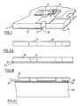
- a typical prior art microwave integrated circuit is shown in Figure 1.
- the substrate typically alumina or beryllia
- a metal coating or layer 12 typically a two-layer coating comprising a metal which adheres to the substrate such as chromium, and a good conductor, such as gold.
- a similar coating on the upper side is formed and shaped by photolithographic and etching techniques to yield the desired circuit geometry 13.
- Various components such as capacitors, resistors and, most important, active devices 14, may be attached at specific locations on the upper circuit. Selected points of the upper circuit are connected to the back side of the substrate by via holes 16 which have metallized walls 17.
- Active devices are typically located in the vicinity of the via holes both because one of their electrodes typically needs to be grounded to the backside metal layer 12 but also in order to help conduct heat generated by the device to the back surface where it is dissipated. However, unless the via holes are solidly filled, the device cannot be located on top of the hole, where it would be most desirable for heat dissipation.
- via holes 21 are drilled by a laser beam in the ceramic substrate 22 at selected locations, Figure 2A.
- the substrate may then be coated with a laminated layer such as a layer including a positive dry film resist 23 carried by a mylar film 24, Figure 2B.
- a suitable laminated layer including a dry film resist polymer is "Resolve" sold by Minnesota Mining and Manufacturing Company.
- the polymer film carried by the mylar preferably has good adherence to both ceramic and glass, and, to some extent, even to the mylar backing.
- the film supported by the mylar backing is preferably covered with a liner which is removed before applying the film to the substrate for lamination.
- the substrate with applied film is then preferably heated whereby the polymer film becomes brittle.
- the mylar backing is then removed.
- the laminating temperature is such as to achieve the desired brittleness and adhesion of the polymer film but avoid completely drying out the film so that by using a higher temperature, a second lamination can be carried out.
- a temperature of around 120 deg.C for the first lamination and 140 deg.C for the second lamination has been used in the case of the above mentioned laminated layered photoresist.
- the desired coverage of the substrate with polymer is achieved by laminating the polymer at a lower temperature, for example 90 deg.C, thereby avoiding brittleness.
- the polymer can then be exposed either through the substrate itself or through a suitable mask and dissolve a way to leave the open holes with a polymer surface layer on the substrate.
- the substrate undergoes a second lamination process during which the substrate, already covered with the polymer film, is attached to a smooth, metallized backing plate, so that one end of the holes is closed by a metal.
- a glass slide 26 is metallized with a thick layer of copper 27 (about 10 microns), followed by a thin layer of gold 28 (about .1 micron).
- the gold layer is used to avoid oxidation while the thick layer of copper provides a low electrical resistance of the metal film as well as ease of etching after the process is completed. Any other suitable metal conductive layer can be used.
- the substrate attached to the backing plate by the polymer layer 23 is ready for a plating operation.
- An electrical contact 31 is made to the metal backing layer which is slightly larger than the substrate, so that a metallized edge 32 will remain uncovered and provide easy electrical contact.
- the substrate, attached to the backing plate is immersed in a plating bath such as a neutral gold bath suitable for low-stress fine grain deposits.
- a plating bath such as a neutral gold bath suitable for low-stress fine grain deposits.
- a plating bath such as a neutral gold bath suitable for low-stress fine grain deposits.
- Several suitable plating solutions are readily available and other metals besides gold might be considered, e.g. copper.
- the walls of the holes are not metallized, the lines of the electric field during plating will be approximately parallel to the hole walls and therefore the plating will take place approximately parallel to the bottom so as to fill the hole uniformly.
- the holes are filled with metal, they start to develop the mushroom shape characteristic of plating not constrained by lateral walls
- the backing plate is separated from the substrate. In the specific embodiment described this is accomplished by etching the relatively thick copper layer deposited on the glass backing. In order to facilitate this operation, no adhesive layer is used on the glass so that the adherence is minimal and the etching solution (e.g. nitric acid) will readily penetrate.
- etching solution e.g. nitric acid
- a variety of alternatives are clearly possible, including using a backing plate which is itself readily etchable, such as an aluminum sheet barely thick enough to provide minimal mechanical integrity. This could be easily etched away, e.g., with a sodium or potassium hydroxyde solution.
- the residues of the gold film 28 and the polymer 23 are removed, e.g. by a combination of ultrasonic and ashing, so that the result of the described process is a substrate with holes filled by a solid column of gold 29.
- the side originally attached to the backing plate is typically fairly planar. The other, especially when some overplating has taken place, may require an additional planarization step. This is easily accomplished by a lapping operation where the surface of the ceramic substrate is hardly modified, since the gold is much softer and readily abraded.
- the substrate at this point appears as in Figure 3 and is ready for metallization and further processing to form a microwave integrated circuit having a metallized lower layer with circuits on the uper layer.
Abstract
Description
- The present invention is directed to a microwave integrated circuit formed on a substrate having via holes for either electrical grounding or heat dissipation or both and more particularly to a substrate including via holes which are filled with metal.
- In the manufacturing of microwave integrated circuits formed on a substrate, it is often desirable to create direct connections between specific points of the circuit on the upper surface and the metallization on the lower surface. Such connections may be required for two different reasons: 1) to create a low inductance/low resistance path to ground; and 2) to provide an effective heat sinking, specifically for active devices. In the present state of the art when the substrate used is a ceramic substrate, such connections are typically obtained by cutting holes, referred to as "via holes" or "vias", through the substrate and by metallizing the wall of the holes. The holes may be cut either before or after processing the substrate. In the first case, the presence of holes significantly hinders the photolithography process, typically preventing the definition of fine details in the neighborhood of a hole. In the second case, the hole cutting process is severely limited by the need to preserve the integrity of the circuit already fabricated. This is especially true in the case of ceramic materials, e.g., alumina, where holes cannot be easily etched chemically and have to be drilled mechanically or by laser. Both processes are damaging to delicate circuit structures. In addition, the metallization of the wall alone may provide an adequate electrical connection but does not generally provide adequate heat conduction in the case of high power devices.
- In the present state-of-the-art, the vias or holes are often filled with a conductive paste ("ink") of the type used in connection with thin film circuits. However, this process is only partially successful because during filling of the holes with the paste and subsequent curing, the volume of the paste is significantly reduced thereby creating voids in the filling.
- It is an object of the present invention to provide a process capable of completely filling with metal the holes or vias in an insulating substrate used in microwave integrated circuits.
- It is another object of the present invention to provide a substrate having via holes which extend between the top and bottom surfaces which are filled with metal to provide good conductive path between the surfaces.
- The foregoing and other objects of the invention are achieved by a substrate comprising a body of insulating material having upper and lower surfaces with one or more holes formed in said body to extend between the upper and the lower surface and a metal filling said holes and extending between the upper and the lower surfaces. The invention is further directed to a method of forming the aforementioned substrate.
- Figure 1 shows a portion of a microwave integrated circuit with metallized via holes in accordance with the prior art.
- Figures 2A-2D show in cross-section, a portion of a substrate and the method of forming metal filled via holes in accordance with the present invention.
- Figure 3 shows a finished substrate with filled via holes ready for metallization and photolithography processing.
- A typical prior art microwave integrated circuit is shown in Figure 1. The
substrate 11, typically alumina or beryllia, is coated on the lower surface with a metal coating orlayer 12, typically a two-layer coating comprising a metal which adheres to the substrate such as chromium, and a good conductor, such as gold. A similar coating on the upper side is formed and shaped by photolithographic and etching techniques to yield the desiredcircuit geometry 13. Various components such as capacitors, resistors and, most important,active devices 14, may be attached at specific locations on the upper circuit. Selected points of the upper circuit are connected to the back side of the substrate by viaholes 16 which havemetallized walls 17. Active devices are typically located in the vicinity of the via holes both because one of their electrodes typically needs to be grounded to thebackside metal layer 12 but also in order to help conduct heat generated by the device to the back surface where it is dissipated. However, unless the via holes are solidly filled, the device cannot be located on top of the hole, where it would be most desirable for heat dissipation. - In the preferred embodiment of the present invention, via
holes 21 are drilled by a laser beam in theceramic substrate 22 at selected locations, Figure 2A. The substrate may then be coated with a laminated layer such as a layer including a positive dry film resist 23 carried by amylar film 24, Figure 2B. A suitable laminated layer including a dry film resist polymer is "Resolve" sold by Minnesota Mining and Manufacturing Company. The polymer film carried by the mylar preferably has good adherence to both ceramic and glass, and, to some extent, even to the mylar backing. The film supported by the mylar backing is preferably covered with a liner which is removed before applying the film to the substrate for lamination. The substrate with applied film is then preferably heated whereby the polymer film becomes brittle. The mylar backing is then removed. When the mylar backing is removed from the film, the film remains adhered to the substrate, however, the brittle portion over the holes is removed with the mylar whereby the substrate will be uniformly coated and the holes remain open. The laminating temperature is such as to achieve the desired brittleness and adhesion of the polymer film but avoid completely drying out the film so that by using a higher temperature, a second lamination can be carried out. As an example, a temperature of around 120 deg.C for the first lamination and 140 deg.C for the second lamination has been used in the case of the above mentioned laminated layered photoresist. - In an alternative embodiment of this invention the desired coverage of the substrate with polymer is achieved by laminating the polymer at a lower temperature, for example 90 deg.C, thereby avoiding brittleness. The polymer can then be exposed either through the substrate itself or through a suitable mask and dissolve a way to leave the open holes with a polymer surface layer on the substrate.
- After the desired coverage of the substrate is achieved with one of the described processes, or any other alternate process which will form a substrate with an adhesive layer, the substrate undergoes a second lamination process during which the substrate, already covered with the polymer film, is attached to a smooth, metallized backing plate, so that one end of the holes is closed by a metal.
- In the preferred embodiment of this invention as shown in Figure 2C, a
glass slide 26 is metallized with a thick layer of copper 27 (about 10 microns), followed by a thin layer of gold 28 (about .1 micron). The gold layer is used to avoid oxidation while the thick layer of copper provides a low electrical resistance of the metal film as well as ease of etching after the process is completed. Any other suitable metal conductive layer can be used. - After the second lamination is completed, the substrate attached to the backing plate by the
polymer layer 23 is ready for a plating operation. An electrical contact 31 is made to the metal backing layer which is slightly larger than the substrate, so that ametallized edge 32 will remain uncovered and provide easy electrical contact. The substrate, attached to the backing plate, is immersed in a plating bath such as a neutral gold bath suitable for low-stress fine grain deposits. Several suitable plating solutions are readily available and other metals besides gold might be considered, e.g. copper. Because the walls of the holes are not metallized, the lines of the electric field during plating will be approximately parallel to the hole walls and therefore the plating will take place approximately parallel to the bottom so as to fill the hole uniformly. After the holes are filled with metal, they start to develop the mushroom shape characteristic of plating not constrained by lateral walls, as shown in Figure 2D, which depicts the cross-section of a portion of the substrate after the plating operation. - At this point the backing plate is separated from the substrate. In the specific embodiment described this is accomplished by etching the relatively thick copper layer deposited on the glass backing. In order to facilitate this operation, no adhesive layer is used on the glass so that the adherence is minimal and the etching solution (e.g. nitric acid) will readily penetrate. A variety of alternatives are clearly possible, including using a backing plate which is itself readily etchable, such as an aluminum sheet barely thick enough to provide minimal mechanical integrity. This could be easily etched away, e.g., with a sodium or potassium hydroxyde solution.
- After removing the backing plate, the residues of the
gold film 28 and thepolymer 23 are removed, e.g. by a combination of ultrasonic and ashing, so that the result of the described process is a substrate with holes filled by a solid column ofgold 29. The side originally attached to the backing plate is typically fairly planar. The other, especially when some overplating has taken place, may require an additional planarization step. This is easily accomplished by a lapping operation where the surface of the ceramic substrate is hardly modified, since the gold is much softer and readily abraded. The substrate at this point appears as in Figure 3 and is ready for metallization and further processing to form a microwave integrated circuit having a metallized lower layer with circuits on the uper layer. - Thus, there has been provided a substrate with metal filled via holes and a method of forming the substrate.
Claims (5)
a body of insulating material having upper and lower surfaces with one or more holes formed in said body to extend between the upper and lower surface; and
a metal filling said holes and extending between and coplanar with the upper and lower surfaces.
forming holes or vias at selected locations in a substrate;
closing one end of said holes or vias with a conductive film which extends on the surface of the substrate;
plating metal through the holes or vias onto said conductive film until the holes or vias are filled with plated metal; and
removing said conductive film to leave a substrate with vias or holes filled with plated metal.
Applications Claiming Priority (2)
| Application Number | Priority Date | Filing Date | Title |
|---|---|---|---|
| US07/251,538 US4925723A (en) | 1988-09-29 | 1988-09-29 | Microwave integrated circuit substrate including metal filled via holes and method of manufacture |
| US251538 | 1988-09-29 |
Publications (3)
| Publication Number | Publication Date |
|---|---|
| EP0362161A2 true EP0362161A2 (en) | 1990-04-04 |
| EP0362161A3 EP0362161A3 (en) | 1990-09-19 |
| EP0362161B1 EP0362161B1 (en) | 1997-03-05 |
Family
ID=22952396
Family Applications (1)
| Application Number | Title | Priority Date | Filing Date |
|---|---|---|---|
| EP89830421A Expired - Lifetime EP0362161B1 (en) | 1988-09-29 | 1989-09-26 | Method of manufacturing a substrate for microwave integrated circuits |
Country Status (5)
| Country | Link |
|---|---|
| US (1) | US4925723A (en) |
| EP (1) | EP0362161B1 (en) |
| JP (1) | JPH02154497A (en) |
| AT (1) | ATE149742T1 (en) |
| DE (1) | DE68927815T2 (en) |
Cited By (3)
| Publication number | Priority date | Publication date | Assignee | Title |
|---|---|---|---|---|
| GB2226707B (en) * | 1988-11-03 | 1993-05-26 | Micro Strates Inc | Ceramic substrate for hybrid microcircuits and method of making the same |
| EP0948049A1 (en) * | 1998-03-03 | 1999-10-06 | Ching-Kuang Tzuang | Dual-mode microwave/millimeter wave integrated circuit package |
| RU2472325C1 (en) * | 2011-05-20 | 2013-01-10 | Игорь Валентинович Колядов | Method of making plated holes in printed-circuit board |
Families Citing this family (18)
| Publication number | Priority date | Publication date | Assignee | Title |
|---|---|---|---|---|
| US5023993A (en) * | 1988-09-30 | 1991-06-18 | Grumman Aerospace Corporation | Method for manufacturing a high-performance package for monolithic microwave integrated circuits |
| US5379515A (en) * | 1989-12-11 | 1995-01-10 | Canon Kabushiki Kaisha | Process for preparing electrical connecting member |
| IT1238150B (en) * | 1990-01-31 | 1993-07-09 | PROCEDURE FOR HOT COUPLING OF THIN STRUCTURES IN SYNTHETIC MATERIALS SUCH AS FABRICS, NON-WOVEN FABRICS, CARPETS AND OTHER, TO MANUFACTURERS IN SYNTHETIC MATERIAL | |
| AU9068491A (en) * | 1990-11-19 | 1992-06-11 | Carborundum Company, The | Microelectronics package |
| US5055966A (en) * | 1990-12-17 | 1991-10-08 | Hughes Aircraft Company | Via capacitors within multi-layer, 3 dimensional structures/substrates |
| JP3166251B2 (en) * | 1991-12-18 | 2001-05-14 | 株式会社村田製作所 | Manufacturing method of ceramic multilayer electronic component |
| JP2707903B2 (en) * | 1992-01-28 | 1998-02-04 | 日本電気株式会社 | Manufacturing method of multilayer printed wiring board |
| US5401913A (en) * | 1993-06-08 | 1995-03-28 | Minnesota Mining And Manufacturing Company | Electrical interconnections between adjacent circuit board layers of a multi-layer circuit board |
| US5761803A (en) * | 1996-06-26 | 1998-06-09 | St. John; Frank | Method of forming plugs in vias of a circuit board by utilizing a porous membrane |
| JPH1032221A (en) * | 1996-07-12 | 1998-02-03 | Nec Corp | Printed wiring board |
| TW396462B (en) * | 1998-12-17 | 2000-07-01 | Eriston Technologies Pte Ltd | Bumpless flip chip assembly with solder via |
| US6284574B1 (en) | 1999-01-04 | 2001-09-04 | International Business Machines Corporation | Method of producing heat dissipating structure for semiconductor devices |
| EP1181239A1 (en) * | 1999-03-31 | 2002-02-27 | Siemens Aktiengesellschaft | Method for producing self-supporting micro-structures, consisting of thin, flat sections or membranes, and use of micro-structures produced by said method as a resistance grid in a device for measuring weak gas flows |
| US6492715B1 (en) | 2000-09-13 | 2002-12-10 | International Business Machines Corporation | Integrated semiconductor package |
| DE10302104A1 (en) * | 2003-01-21 | 2004-08-05 | Friwo Gerätebau Gmbh | Process for the production of circuit carriers with integrated passive components |
| ATE362694T1 (en) * | 2003-05-16 | 2007-06-15 | Friwo Mobile Power Gmbh | POWER SUPPLY CIRCUIT WITH THREE-DIMENSIONAL CIRCUIT CARRIERS AND MANUFACTURING METHOD |
| US7166877B2 (en) * | 2004-07-30 | 2007-01-23 | Bae Systems Information And Electronic Systems Integration Inc. | High frequency via |
| US8362368B2 (en) * | 2009-04-27 | 2013-01-29 | Ultrasource, Inc. | Method and apparatus for an improved filled via |
Citations (6)
| Publication number | Priority date | Publication date | Assignee | Title |
|---|---|---|---|---|
| GB2046514A (en) * | 1979-04-09 | 1980-11-12 | Raytheon Co | Semiconductor device |
| US4396467A (en) * | 1980-10-27 | 1983-08-02 | General Electric Company | Periodic reverse current pulsing to form uniformly sized feed through conductors |
| US4667219A (en) * | 1984-04-27 | 1987-05-19 | Trilogy Computer Development Partners, Ltd. | Semiconductor chip interface |
| WO1987004316A1 (en) * | 1986-01-03 | 1987-07-16 | Motorola, Inc. | Ultra high density pad array chip carrier |
| US4731701A (en) * | 1987-05-12 | 1988-03-15 | Fairchild Semiconductor Corporation | Integrated circuit package with thermal path layers incorporating staggered thermal vias |
| EP0329133A2 (en) * | 1988-02-19 | 1989-08-23 | Microelectronics and Computer Technology Corporation | Flip substrate for chip mount |
Family Cites Families (2)
| Publication number | Priority date | Publication date | Assignee | Title |
|---|---|---|---|---|
| US3205298A (en) * | 1963-03-25 | 1965-09-07 | Charles G Kalt | Printed circuit board |
| US3562009A (en) * | 1967-02-14 | 1971-02-09 | Western Electric Co | Method of providing electrically conductive substrate through-holes |
-
1988
- 1988-09-29 US US07/251,538 patent/US4925723A/en not_active Expired - Lifetime
-
1989
- 1989-09-26 EP EP89830421A patent/EP0362161B1/en not_active Expired - Lifetime
- 1989-09-26 DE DE68927815T patent/DE68927815T2/en not_active Expired - Fee Related
- 1989-09-26 AT AT89830421T patent/ATE149742T1/en not_active IP Right Cessation
- 1989-09-26 JP JP1250382A patent/JPH02154497A/en active Pending
Patent Citations (6)
| Publication number | Priority date | Publication date | Assignee | Title |
|---|---|---|---|---|
| GB2046514A (en) * | 1979-04-09 | 1980-11-12 | Raytheon Co | Semiconductor device |
| US4396467A (en) * | 1980-10-27 | 1983-08-02 | General Electric Company | Periodic reverse current pulsing to form uniformly sized feed through conductors |
| US4667219A (en) * | 1984-04-27 | 1987-05-19 | Trilogy Computer Development Partners, Ltd. | Semiconductor chip interface |
| WO1987004316A1 (en) * | 1986-01-03 | 1987-07-16 | Motorola, Inc. | Ultra high density pad array chip carrier |
| US4731701A (en) * | 1987-05-12 | 1988-03-15 | Fairchild Semiconductor Corporation | Integrated circuit package with thermal path layers incorporating staggered thermal vias |
| EP0329133A2 (en) * | 1988-02-19 | 1989-08-23 | Microelectronics and Computer Technology Corporation | Flip substrate for chip mount |
Non-Patent Citations (1)
| Title |
|---|
| IBM TECHNICAL DISCLOSURE BULLETIN. vol. 21, no. 4, September 1978, NEW YORK US pages 1396 - 1397; D. Tomsa et al.: "MULTILAYER LAMINATED CHIP CARRIER" * |
Cited By (3)
| Publication number | Priority date | Publication date | Assignee | Title |
|---|---|---|---|---|
| GB2226707B (en) * | 1988-11-03 | 1993-05-26 | Micro Strates Inc | Ceramic substrate for hybrid microcircuits and method of making the same |
| EP0948049A1 (en) * | 1998-03-03 | 1999-10-06 | Ching-Kuang Tzuang | Dual-mode microwave/millimeter wave integrated circuit package |
| RU2472325C1 (en) * | 2011-05-20 | 2013-01-10 | Игорь Валентинович Колядов | Method of making plated holes in printed-circuit board |
Also Published As
| Publication number | Publication date |
|---|---|
| ATE149742T1 (en) | 1997-03-15 |
| US4925723A (en) | 1990-05-15 |
| JPH02154497A (en) | 1990-06-13 |
| EP0362161A3 (en) | 1990-09-19 |
| DE68927815D1 (en) | 1997-04-10 |
| EP0362161B1 (en) | 1997-03-05 |
| DE68927815T2 (en) | 1997-09-04 |
Similar Documents
| Publication | Publication Date | Title |
|---|---|---|
| US4925723A (en) | Microwave integrated circuit substrate including metal filled via holes and method of manufacture | |
| US5369881A (en) | Method of forming circuit wiring pattern | |
| US6291779B1 (en) | Fine pitch circuitization with filled plated through holes | |
| US5454928A (en) | Process for forming solid conductive vias in substrates | |
| US5406446A (en) | Thin film capacitor | |
| TWI307142B (en) | Semiconductor package substrate having different thicknesses between wire bonding pad and ball pad and method for fabricating the same | |
| US20050020079A1 (en) | Structure having flush circuit features and method of making | |
| JPS639376B2 (en) | ||
| EP0099544A1 (en) | Method for forming conductive lines and via studs on LSI carrier substrates | |
| US20060255009A1 (en) | Plating method for circuitized substrates | |
| JP2010529694A (en) | Circuit assembly comprising a metal core substrate and process for making the circuit assembly | |
| JP4282777B2 (en) | Semiconductor device substrate and semiconductor device manufacturing method | |
| JP2004031710A (en) | Method for manufacturing wiring board | |
| JP3238685B2 (en) | Method of manufacturing integrated microwave assembly | |
| US5023994A (en) | Method of manufacturing a microwave intergrated circuit substrate including metal lined via holes | |
| US4703392A (en) | Microstrip line and method for fabrication | |
| JP2004087862A (en) | Tape carrier for semiconductor device | |
| US4600663A (en) | Microstrip line | |
| KR100593211B1 (en) | Method for manufacturing through hole electrode for wafer | |
| JPS6035543A (en) | Manufacture of semiconductor device | |
| JPS6372193A (en) | Circuit board | |
| JP2664409B2 (en) | Manufacturing method of hybrid integrated circuit | |
| JP3002307B2 (en) | Method for manufacturing flexible circuit board for testing circuit components | |
| JPS6372189A (en) | Manufacture of circuit board | |
| JPH10178141A (en) | Composite lead frame and its manufacturing method |
Legal Events
| Date | Code | Title | Description |
|---|---|---|---|
| PUAI | Public reference made under article 153(3) epc to a published international application that has entered the european phase |
Free format text: ORIGINAL CODE: 0009012 |
|
| AK | Designated contracting states |
Kind code of ref document: A2 Designated state(s): AT BE CH DE ES FR GB GR IT LI LU NL SE |
|
| PUAL | Search report despatched |
Free format text: ORIGINAL CODE: 0009013 |
|
| AK | Designated contracting states |
Kind code of ref document: A3 Designated state(s): AT BE CH DE ES FR GB GR IT LI LU NL SE |
|
| 17P | Request for examination filed |
Effective date: 19910207 |
|
| 17Q | First examination report despatched |
Effective date: 19921217 |
|
| GRAG | Despatch of communication of intention to grant |
Free format text: ORIGINAL CODE: EPIDOS AGRA |
|
| GRAH | Despatch of communication of intention to grant a patent |
Free format text: ORIGINAL CODE: EPIDOS IGRA |
|
| GRAH | Despatch of communication of intention to grant a patent |
Free format text: ORIGINAL CODE: EPIDOS IGRA |
|
| GRAA | (expected) grant |
Free format text: ORIGINAL CODE: 0009210 |
|
| AK | Designated contracting states |
Kind code of ref document: B1 Designated state(s): AT BE CH DE ES FR GB GR IT LI LU NL SE |
|
| PG25 | Lapsed in a contracting state [announced via postgrant information from national office to epo] |
Ref country code: NL Free format text: LAPSE BECAUSE OF FAILURE TO SUBMIT A TRANSLATION OF THE DESCRIPTION OR TO PAY THE FEE WITHIN THE PRESCRIBED TIME-LIMIT Effective date: 19970305 Ref country code: LI Effective date: 19970305 Ref country code: GR Free format text: LAPSE BECAUSE OF FAILURE TO SUBMIT A TRANSLATION OF THE DESCRIPTION OR TO PAY THE FEE WITHIN THE PRESCRIBED TIME-LIMIT Effective date: 19970305 Ref country code: ES Free format text: THE PATENT HAS BEEN ANNULLED BY A DECISION OF A NATIONAL AUTHORITY Effective date: 19970305 Ref country code: CH Effective date: 19970305 Ref country code: BE Effective date: 19970305 Ref country code: AT Effective date: 19970305 |
|
| REF | Corresponds to: |
Ref document number: 149742 Country of ref document: AT Date of ref document: 19970315 Kind code of ref document: T |
|
| REG | Reference to a national code |
Ref country code: CH Ref legal event code: EP |
|
| REF | Corresponds to: |
Ref document number: 68927815 Country of ref document: DE Date of ref document: 19970410 |
|
| ITF | It: translation for a ep patent filed |
Owner name: STUDIO FERRARIO |
|
| PG25 | Lapsed in a contracting state [announced via postgrant information from national office to epo] |
Ref country code: SE Effective date: 19970605 |
|
| ET | Fr: translation filed | ||
| NLV1 | Nl: lapsed or annulled due to failure to fulfill the requirements of art. 29p and 29m of the patents act | ||
| REG | Reference to a national code |
Ref country code: CH Ref legal event code: PL |
|
| PG25 | Lapsed in a contracting state [announced via postgrant information from national office to epo] |
Ref country code: LU Free format text: LAPSE BECAUSE OF NON-PAYMENT OF DUE FEES Effective date: 19970926 |
|
| PLBE | No opposition filed within time limit |
Free format text: ORIGINAL CODE: 0009261 |
|
| STAA | Information on the status of an ep patent application or granted ep patent |
Free format text: STATUS: NO OPPOSITION FILED WITHIN TIME LIMIT |
|
| 26N | No opposition filed | ||
| REG | Reference to a national code |
Ref country code: GB Ref legal event code: IF02 |
|
| PGFP | Annual fee paid to national office [announced via postgrant information from national office to epo] |
Ref country code: FR Payment date: 20030828 Year of fee payment: 15 |
|
| PGFP | Annual fee paid to national office [announced via postgrant information from national office to epo] |
Ref country code: GB Payment date: 20030905 Year of fee payment: 15 |
|
| PGFP | Annual fee paid to national office [announced via postgrant information from national office to epo] |
Ref country code: DE Payment date: 20030930 Year of fee payment: 15 |
|
| PG25 | Lapsed in a contracting state [announced via postgrant information from national office to epo] |
Ref country code: GB Free format text: LAPSE BECAUSE OF NON-PAYMENT OF DUE FEES Effective date: 20040926 |
|
| PG25 | Lapsed in a contracting state [announced via postgrant information from national office to epo] |
Ref country code: DE Free format text: LAPSE BECAUSE OF NON-PAYMENT OF DUE FEES Effective date: 20050401 |
|
| GBPC | Gb: european patent ceased through non-payment of renewal fee |
Effective date: 20040926 |
|
| PG25 | Lapsed in a contracting state [announced via postgrant information from national office to epo] |
Ref country code: FR Free format text: LAPSE BECAUSE OF NON-PAYMENT OF DUE FEES Effective date: 20050531 |
|
| REG | Reference to a national code |
Ref country code: FR Ref legal event code: ST |
|
| PG25 | Lapsed in a contracting state [announced via postgrant information from national office to epo] |
Ref country code: IT Free format text: LAPSE BECAUSE OF NON-PAYMENT OF DUE FEES Effective date: 20050926 |