EP0364110A2 - Semiconductor memory device having a serial access memory - Google Patents
Semiconductor memory device having a serial access memory Download PDFInfo
- Publication number
- EP0364110A2 EP0364110A2 EP89309443A EP89309443A EP0364110A2 EP 0364110 A2 EP0364110 A2 EP 0364110A2 EP 89309443 A EP89309443 A EP 89309443A EP 89309443 A EP89309443 A EP 89309443A EP 0364110 A2 EP0364110 A2 EP 0364110A2
- Authority
- EP
- European Patent Office
- Prior art keywords
- address
- serial access
- redundancy
- data
- generating means
- Prior art date
- Legal status (The legal status is an assumption and is not a legal conclusion. Google has not performed a legal analysis and makes no representation as to the accuracy of the status listed.)
- Granted
Links
Images


Classifications
-
- G—PHYSICS
- G11—INFORMATION STORAGE
- G11C—STATIC STORES
- G11C11/00—Digital stores characterised by the use of particular electric or magnetic storage elements; Storage elements therefor
- G11C11/21—Digital stores characterised by the use of particular electric or magnetic storage elements; Storage elements therefor using electric elements
- G11C11/34—Digital stores characterised by the use of particular electric or magnetic storage elements; Storage elements therefor using electric elements using semiconductor devices
-
- G—PHYSICS
- G11—INFORMATION STORAGE
- G11C—STATIC STORES
- G11C7/00—Arrangements for writing information into, or reading information out from, a digital store
- G11C7/10—Input/output [I/O] data interface arrangements, e.g. I/O data control circuits, I/O data buffers
- G11C7/1006—Data managing, e.g. manipulating data before writing or reading out, data bus switches or control circuits therefor
Abstract
Description
- The present invention generally relates to a semiconductor memory device, and more particularly to a semiconductor memory device having a serial access memory.
- Generally, an image memory used in the field of image processing has two ports of a random port and a serial port. The random port is connected to a central processing unit (hereinafter simply referred to as a CPU), and the serial port is connected to a display device such as a cathode-ray tube display device. The access speed at the serial port is desired to be as fast as possible since it directly influences the image displaying speed. Particularly, there is a need to use a higher-access speed image memory as an image memory used for high-speed image processing for drawing pictures at high speeds.
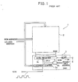
- Referring to FIG.1, there is illustrated a conventional semiconductor memory device having a serial access memory. Referring to FIG.1, a
semiconductor memory device 1 includes a random access memory (hereinafter simply referred to as a RAM) 2, and a serial access memory (hereinafter simply referred to as a SAM) 3. TheRAM 2 includes memory cells located at intersecting points where word lines and bit lines intersect. One of the word lines is selected by a row address supplied from an external device such as a CPU, and one of the bit lines is selected by a column address supplied therefrom. TheSAM 3 is made up of anaddress counter 3a, aredundancy decision circuit 3b, adata register 3c, and an input/output buffer 3d. Theaddress counter 3a inputs, as an initial address value for serial access, the column address in synchronism with a rise of a serial access strobe signal SAS, and generates a corresponding serial access address SAAD. Theredundancy decision circuit 3b compares the serial access address SAAD with a predetermined redundancy address, and outputs a redundancy switching signal SAM when the compared addresses are identical to each other. Thedata register 3c has storage (register) cells and redundancy cells amounting to one line of theRAM 2. The storage cells are accessed one by one in series in synchronism with the redundancy address SAAD. When the redundancy switching signal SOM is supplied to thedata register 3c, the redundancy cells are accessed. The serial input/output buffer 3d connects thedata register 3c and an input/output terminal 4 in the bidirection. - However, the conventional device as shown in FIG.1 presents the following disadvantages. The
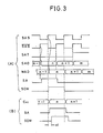
address counter 3a inputs the column address labelled CAD in synchronism with a rise of the serial access strobe signal SAS, as shown in FIG.3(B). In rather words, a timing with which the column address is input corresponds to the rise of the serial access strobe signal SAS. Then theaddress counter 3a outputs the serial access address SAAD, and then theredundancy decision circuit 3b outputs the redundancy switching signal SOM to thedata register 3c. Thus, the serial access speed of the device is not so high. - It is inevitable that a large storage capacity memory device is configured so as to have a redundancy structure and therefore redundancy decision procedure is necessarily required. In the redundancy decision procedure, an address for cells requested to be accessed is compared with the redundancy address which is programmed information indicative of defective cells, and a decision is made based on whether both the addresses are the same. It is noted that the above-mentioned redundancy decision procedure cannot be done until the address of cells requested for accessing, that is, the serial access address SAAD is settled. In the above-mentioned manner, the serial access cannot be done until the serial access address SAAD is settled and then the redundancy decision procedure is executed. Even when the length of a period of the serial access strobe signal SAS is reduced in order to speed up the serial access, there is a limit on the possible length of period due to a time necessary for the settlement of the serial access address SAAD and the redundancy decision procedure. The above description holds true for an alternative in which the column address CAD is input in the
address counter 3a in synchronism with a fall of the serial access strobe signal SAS. - Accordingly, a general object of the present invention is to provide an improved semiconductor memory device having a serial access memory in which the aforementioned disadvantages are eliminated.
- Another object of the present invention is to provide a higher-speed semiconductor memory device having a serial access memory in which serial access is done immediately after the serial access signal falls or rises, or in other words, the column address is input in the address counter so that the length of a period of the serial access signal can be reduced and serial access speed can be increased.
- The above objects of the present invention can be achieved by a semiconductor memory device comprising a random access memory including a plurality of memory cells and parallel read/write means for writing data and reading data into and from the memory cells on the basis of address information, and a serial access memory coupled to the random access memory. The serial access memory comprises data register means for storing data to be written into or read from the random access memory and to be input from or output to an external signal line in serial form, the data register means including a first group of register cells and a second group of redundancy cells, first address generating means for generating a first serial access address starting from an initial address supplied from an external device, and second address generating means, coupled to the first address generating means, for inputting the first serial access address and generating a second serial access address to be supplied to the data register means, the first serial access address having the same contents as the second serial access address and preceding the second serial access address by a predetermined time. The serial access memory further comprises redundancy decision means, coupled to the first address generating means, for determining whether the first serial access address is the same as a redundancy address, and selecting means, coupled to the redundancy decision means, for selecting one of the first and second groups of the data register means on the basis of the comparison result supplied from the redundancy decision means, the data registered in the data register means being accessed in serial form by the second serial access address. When the second serial access address is supplied to the data register means, the data is input in or output from the data register means in series.
- The aforementioned objects of the present invention can also be achieved by a semiconductor memory device comprising a random access memory including a plurality of memory cells and parallel read/write means for writing data and reading data into and from the memory cells on the basis of address information, and a serial access memory coupled to the random access memory. The address information is divided into groups each composed of a predetermined number of address bits. The serial access memory comprises data register means for storing data to be written into or read from the random access memory and to be input from or output to an external signal line in serial form, the data register means including a first group of register cells and a second group of redundancy cells, first address generating means, provided for each of the groups of address bits, for generating a part of a first serial access address starting from an initial address for corresponding one of the groups of address bits supplied from an external device, and second address generating means, provided for each of the groups of address bits and coupled to the related first address generating means, for inputting the related part of the first serial access address and generating a part of a second serial access address to be supplied to the data register means, the first serial access address having the same contents as the second serial access address and preceding the second serial access address by a predetermined time. The serial access memory further comprises redundancy decision means, provided for each of the groups of address bits and coupled to the first address generating means, for determining whether the part of the first serial access address is the same as a corresponding part of a redundancy address, and selecting means, coupled to the redundancy decision means, for selecting one of the first and second groups of the data register means on the basis of the comparison results supplied from the redundancy decision means provided for the groups of address bits, the data registered in the data register means being accessed in serial form by the second serial access address. When the second serial access address is supplied to the data register means, the data is input in or output from the data register means in series.
- The aforementioned objects of the present invention can also be achieved by a semiconductor memory device comprising a memory cell array including a plurality of memory cells, redundancy memory cells replaceable by defective memory cells contained in the memory cell array, a data register coupled to the memory cell array and including a plurality of register cells, the data register storing a plurality of bits read out from the memory cell array, a redundancy register coupled to the redundancy memory cells and storing data read out from the redundancy memory cells, selecting means for selecting one register cell from among the plurality of register cells on the basis of a serial access address, first address generating means, coupled to the selecting means, for sequentially generating the serial access address, second address generating means, coupled to the first address generating means, for sequentially generating the serial access address prior to the first address generating means, means for determining whether the serial access address generated by the second address generating means coincides with an address indicative of one of the redundancy memory cells, and output means, coupled to the data register and the redundancy register, for outputting the data stored in the redundancy register in place of data stored in the data register when the means detects the coincidence.
- The aforementioned objects of the present invention can also be achieved by a semiconductor memory device comprising a register including a plurality of data registers and storing data composed of a plurality of bits to be output in serial form, output means for sequentially designating the plurality of data registers and sequentially outputting the plurality of bits, a redundancy register replaceable by one of the plurality of data registers, address generating means for simultaneously generating a first address for sequentially designating the plurality of data registers and a second address corresponding to an address obtained by incrementing the first address by +1, detecting means for detecting the coincidence of the second address and a predetermined address, and switching means for responding to the detected coincidence and selecting data stored in the redundancy register in place of the one of the data registers.
- Additional objects, features and advantages of the present invention will be apparent from the following detailed description when read in conjunction with the accompanying drawings.
-
- FIG.1 is a block diagram of a conventional semiconductor memory device having a serial access memory;
- FIG.2 is a block diagram of the principle of the present invention;
- FIG.3 is a timing chart of signals observed in the configuration shown in FIG.2 and the conventional device shown in FIG.1;
- FIG.4 is a block diagram of a fundamental structure of the invention which handles a plurality of address bits;
- FIG.5 is a timing chart of signals observed in the configuration shown in FIG.4;
- FIG.6 is a block diagram of a fundamental structure of the present invention where an address signal is divided into groups each consisting of bits;
- FIG.7 is a timing chart of signals observed in the configuration shown in FIG.6;
- FIG.8 is a block diagram of the entire structure of a semiconductor memory device according to a preferred embodiment of the present invention;
- FIG.9 is a block diagram of a decoder, a data register and a peripheral circuit thereof;
- FIG.10 is a circuit diagram of an address counter used in the embodiment shown in FIG.8;
- FIG.11 is a circuit diagram of a flip-flop used in the address counter shown in FIG.10; and
- FIG.12 is a circuit diagram of a redundancy decision circuit and a gate and latch circuit used in the embodiment shown in FIG.8.
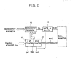
- A description is given of the principle of the present invention with reference to FIG.2. The configuration shown in FIG.2 corresponds to a serial access memory provided in a semiconductor memory device according to the present invention. The illustrated configuration includes a
first counter 10, asecond counter 11, aredundancy decision circuit 12, and a gate andlatch circuit 13. Thefirst counter 10 is supplied with a column address CAD, an initial counter address setting signal SAT, and an inverted serial access strobe signalSAS . The signal SAT is supplied from an external device such as a CPU. The inverted serial access strobe signalSAS is generated in the semiconductor memory device, and is 180 degrees out of phase with the serial access strobe signal SAS which is supplied to thesecond counter 11 and the gate andlatch circuit 13. The signalSAS rises at the same time as the signalSAS falls or vice versa. The first andsecond counters second counters first counter 10 inputs the column address CAD therein as the initial address. The input column address is output to thesecond counter 11 as a slave address signal SAD. Thesecond counter 11 inputs the slave address signal SAD in synchronism with the rise of the serial access strobe signal SAS, and then outputs the slave address signal SAD as a master address signal MAD. As will be described later, the slave address SAD precedes the master address MAD by half the period of the serial access strobe signal SAS. Thefirst counter 10 counts up the column address CAD and outputs the slave address signal SAD each time the inverted serial address strobe signalSAS rises. - Referring to a timing chart of FIG.3(A), the slave address signal SAD derived from the
first counter 10 is renewed each time the inverted serial access strobe signalSAS rises, that is, each time the serial access strobe signal SAS falls. The master address MAD derived from thesecond counter 11 is renewed each time the serial access strobe signal SAS rises. Theredundancy decision circuit 12 makes a decision on redundancy on the basis of the slave address SAD and the redundancy address supplied from a read only memory (not shown in FIG.2) provided in the semiconductor memory device. The redundancy decision procedure is started before the serial access strobe signal SAS rises. Theredundancy decision circuit 12 outputs a signal SA which indicates the decision result when both the input addresses are the same. When the serial access strobe signal SAS rises, the gate andlatch circuit 13 is made open whereby it passes the signal SA as the redundancy switching signal SOM. At almost the same time, the master address MAD is output from thesecond counter 11. When a data register corresponding to the data register 3c shown in FIG.1 is being accessed by the master address MAD and the redundancy switching signal SOM is being output, one of the redundancy cells provided in the data register is selected and the serial access to the selected redundancy cell is executed. Thus, the serial access is started immediately after the master address MAD and the serial access strobe signal SAS are supplied to the data register. As a result, it is possible to reduce the period of the serial access strobe signal SAS so that the serial access speed can be increased. - In the case of FIG.3A, it should be appreciated that the decision result SA for the address ′n′ is obtained by almost a half of the period than the master address MAD corresponding to the address SAAD is incremented to the address ′n′, and the redundancy switching signal SOM (the decision result) is obtained at almost the same time as the master address MAD is changed to the address ′n′. As a result, as shown in FIG.3, the serial access speed is Δt faster than the serial access speed of the conventional device per once addressing.
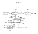
- FIG.4 is a block diagram of a serial access memory in which the column address CAD consists of n bits. Referring to FIG.4, an
address counter 20 is made up of n pairs of the first andsecond counters second counters address counter 20 outputs the serial access strobe signal SAD consisting of n bits and the master address MAD consisting of n bits. Aclock generator 21 generates a clock signal ø having the same timing as the serial access strobe signal SAS, and a clock signalø obtained by inverting the clock signal ø. - As shown in FIG.5, the slave address SAD consisting of n bits is output in synchronism with the rise of the clock signal
ø , that is, the fall of the serial access strobe signal SAS. The master address MAD consisting of n bits is output in synchronism with the rise of the clock signal ø, that is, the rise of the serial access strobe signal SAS. Thus, it is possible to start a necessary internal operation including the redundancy decision procedure before the serial access strobe signal SAS rises. As a result, it is possible to reduce the period of the serial access strobe signal SAS and thus speed up accessing. - In the aforementioned operation, the master address MAD to be supplied to the data register is settled in synchronism with each rise of the serial access strobe signal SAS. Alternatively, it is possible to supply the master address MAD to the data register in synchronism with each fall of the serial access strobe signal SAS.
- In some of conventional memory devices, the column address (initial setting address) supplied to the serial access memory is predecoded by a column decoder provided on the side of the RAM, and is divided into groups. A configuration shown in FIG.6 is suitable for such cases.
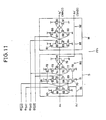
- Referring to FIG.6, an
address counter 30 includes a group-A counter 30a for low-order address bits and a group-B counter 30b for high-order address bits. That is, the column address is divided into two groups of group A and group B. The number of groups is not limited to two. The group-A counter 30a includes master-slave type flip-flops 31a - 31n which amount to the number of bits contained in the group A, and acarry circuit 32 which outputs a carry QA in response to a master output supplied from the flip-flop 31n. A letter ′M′ denotes a master part, and a letter ′S′ denotes a slave part. The group-B counter 30b includes master-slave type flip-flops 33a - 33m amounting to the number of bits contained in the group B. Ashift clock generator 34 relates to the group A, and generates a clock signal ø₁ with the same timing as the serial access strobe signal SAS, and aclock signal ø shift clock generator 35 relates to the group B, and generates a clock signal ø₁ with the same timing as the serial access strobe signal SAS and aclock signal ø carry circuit 32. Aredundancy decision circuit 36 is provided with the bits supplied from the slave part of the flip-flops 31a - 31n, and a group-A redundancy address supplied from a ROM (not shown) provided in the memory device. Aredundancy decision circuit 37 is provided with the bits supplied from the slave part of the flip-flops 33a - 33m, and a group-B redundancy address supplied from the ROM. The decision results AG and BG which are derived from theredundancy decision circuits latch circuit 38, which outputs the redundancy switching signal SOM based on the results AG and BG when the serial access strobe signal SAS rises. - Referring to FIG.7, the slave address SAD related to the group A is renewed each time the
clock signal ø carry circuit 32 outputs the carry QA. In response to the carry QA, the slave address SAD related to the group B is renewed when theclock signal ø clock signal ø - FIG.8 is a diagram of the entire structure of a semiconductor memory device according to a preferred embodiment of the present invention. Referring to FIG.8, the memory device includes a
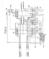
RAM 40 and a SAM (serial access memory) 41. TheRAM 40 is configured as follows. TheRAM 40 is supplied with an external address signal which has been multiplexed. Anaddress buffer 42 receives the external address signal and separately outputs a row address signal and a column address signal. Arow decoder 44 decodes the row address signal, and selects one word line from among a plurality of word lines provided in amemory cell array 43 where a plurality of memory cells MC are arranged in an array. Some of the memory cells are redundancy cells located at a predetermined area in thememory cell array 43. The redundancy cells are replaceable with defective cells in thememory cell array 43. Acolumn decoder 45 decodes the column address signal, and selects one bit line out of a plurality of bit lines in thememory cell array 43. A sense amplifier and I/O gate 46 amplifies the potential of the selected bit line, and performs data reading and writing. An input/output buffer 48 is interposed between a random input/output terminal 47 and the sense amplifier and I/O gate 46 and passes parallel data in the bidirection. - A
clock generator 49a is supplied from an external device such as a CPU with a row address strobe signalRAS , a column address strobe signalCAS , a write enable signalWE , and a transfer signalTR . The transfer signalTR instructs theRAM 40 and theSAM 41 to operate in synchronism with each other. Theclock generator 49a generates the initial counter address setting signal SAT, which is supplied to aclock generator 49b related to theserial access memory 41. Further, theclock generator 49a generates various control signals, which are supplied to aRAM port 57 coupled to the terminal 47. - On the other hand, the serial access memory (SAM) 41 is configured as follows. The
clock generator 49b receives the initial counter address setting signal SAT from theclock generator 49a and the serial access strobe signal supplied from the CPU for example, and generates the following clock signals. That is, theclock generator 49b generates a clock signal øSAT of the same timing as the initial counter address setting signal SAT, a clock signaløSAT which is an inverted signal of the signal SAT, a clock signal øSAS having the same timing as the serial access strobe signal SAS, and a clock signaløSAS which is an inverted signal of the signal SAS. Anaddress counter 50 receives the column address signal and all the clock signals supplied from theclock generator 49b, and outputs the slave address SAD and the master address MAD. Aredundancy decision circuit 51 compares the slave address signal SAD with a redundancy address signal supplied from a read only memory (ROM) 49c, and outputs a redundancy decision signal SH. The redundancy address signal indicates the redundancy cells provided in thememory cell array 43. A gate andlatch circuit 52 temporarily stores the redundancy decision circuit SH, and outputs the same as the redundancy switching signal SOM to adecoder 54. - The
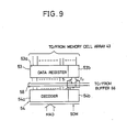
decoder 54 consists of first andsecond decoders 54a and 54b as shown in FIG.9. When the redundancy switching signal SOM is inactive, thefirst decoder 54a is selected. On the other hand, when the redundancy switching signal SOM is active, the second decoder 54b is selected. Each bit of the decoder output is supplied with the gates of two MOS transistors T1 and T2, which are coupled to corresponding signal lines of abus 58. A data register 53 has a storage capacity equal to one line of thememory cell array 43, and includes agroup 53a of register cells and agroup 53b of redundancy register cells, each of which is coupled to a corresponding pair of MOS transistors such as T1 and T2. The redundancy register cells are coupled to the corresponding redundancy cells provided in thememory cell array 43. Thedecoder 54 selects one of the register cells on the basis of the supplied master address MAD. The data register 53 is connected to the bit lines of thememory cell array 43. Turning to FIG.8, a serial input/output buffer 56 is interposed between a serial input/output terminal 55 coupled to an external data line (not shown) and the data register 53, and passes serial data in the bidirection. - FIG.10 is a circuit diagram of the
address counter 50. Theaddress counter 50 is made up of master-slave type flip-flops FF₀ - FFn which amount to the number of bits of the column address signal. - FIG.11 is a circuit diagram of the master-slave type flip-flop FF₀. Each of the other flip-flops FF₁ - FFn is configured in the same manner as the flip-flop FF₀. A slave part S of the flip-flop FF₀ includes a
first gate 64, asecond gate 71 and a slave-side flip-flop 80. Thefirst gate 64 is made up of two P-channel MOS transistors channel MOS transistors 62, 63, which are totem pole connected. Thesecond gate 71 is made up of three P-channel MOS transistors channel MOS transistors flop 80 is made up of four P-channel MOS transistors channel MOS transistors first gate 64 inputs a bit A₀ of the column address signal when the clock signal øSAT is "L (low)" and the clock signaløSAT is "H (high)". The slave-side flip-flop 80 latches the input address bit A₀ when the clock signal øSAS switches from "H" to "L" (in other words, the clock signaløSAS switches from "L" to "H"), that is, when the serial access strobe signal SAS falls.. Then the slave-side flip-flop 80 outputs the latched bit A₀ as a bit A₀′ (SAD) to a master part M of the flip-flop FF₀ and theredundancy decision circuit 51 shown in FIG.8. - The master part M includes a
first gate 85, and a master-side flip-flop 92. Thefirst gate 85 is made up of two P-channel MOS transistors 81, 82, and two N-channel MOS transistors 83, 84, which are totem pole connected. The master-side flip-flop 92 is made up of three P-channel MOS transistors channel MOS transistors flop 92 latches the bit A₀ from the slave part S, when the clock signal øSAS changes from "L" to "H" (in other words, the clock signaløSAS changes from "H" to "L"), that is, when the the serial access strobe signal SAS rises. Then the master-side flip-flop 92 outputs the latched bit A₀′ as a bit A₀˝ (MAD) to the decoder 54 (FIG.8). - FIG.12 is a circuit diagram of the
redundancy decision circuit 51 and the gate andlatch circuit 52. The redundancy decision circuit 51 n exclusive-NOR gates EN₁ - ENn, a single n-input NAND gate 93. Theredundancy decision circuit 51 compares the slave address SAD (A₀′ - An′) with the redundancy address (fuse address F₀ - Fn) supplied from theROM 49c. When both the addresses are the same as each other, theredundancy decision circuit 51 outputs the redundancy decision signal SH. The gate andlatch circuit 52 includes afirst gate 98, a flip-flop 105 and anoutput inverter gate 108. Thefirst gate 98 is made up of two P-channel transistors channel transistors 96, 97, which are totem pole connected. The flip-flop 105 is made up of three P-channel MOS transistors channel MOS transistors 102, 103 and 104. Theoutput inverter gate 108 is made up of a P-channel MOS transistor 106 and an N-channel MOS transistor 107. The gate andlatch circuit 52 latches the redundancy decision signal SH from theredundancy decision circuit 51 when the clock signal øSAS changes from "L" to "H" (or the clock signaløSAS changes "H" to "L"), that is, when the serial access strobe signal SAS rises. Then theredundancy decision circuit 52 outputs, as the redundancy switching signal SOM, the latched signal SH to thedecoder 54 shown in FIG.8. - A description is given of an operation of the embodiment. When the serial access to the
SAM 41 is requested, the initial counter address setting signal SAT is set to "L". Thereby, the clock signal øSAT is switched to "L" and the clock signaløSAT is switched to "H". Thus, the flip-flops FF₀ - FFn shown in FIG.10 input the column address bits (A₀ - An) as the initial address value. The slave part of theaddress counter 50 latches the address bits A₀ - An in synchronism with a fall of the serial access strobe signal SAS, and simultaneously outputs the slave address SAD (A₀′ - An′). Theaddress counter 50 latches the slave address SAD on the master side thereof when the serial access strobe signal SAS rises, and simultaneously outputs the master address MAD (A₀˝ - An˝). Theredundancy decision circuit 51 determines whether the slave address SAD supplied from theaddress counter 50 coincides with the redundancy address F₀ - Fn. The redundancy decision signal SH indicative of the comparison result is supplied to the gate andlatch circuit 52, which latches the result SH when the serial access strobe signal SAS rises, and outputs the same as the redundancy switching signal SOM. - In the aforementioned manner, it is possible to start the internal operation such as address setting for the redundancy decision procedure and the redundancy decision procedure from the fall (rise) of the serial access strobe signal SAS and to complete the same when the signal SAS rises (falls). Thus, the serial access operation can be started when the serial access strobe signal SAS rises (falls). This means that the length of a period of the serial access strobe signal SAS can be reduced and thus the access speed can be increased.
- The present invention is not limited to the aforementioned embodiments, and variations and modifications may be made without departing from the scope of the present invention.
Claims (22)
a random access memory (40) including a plurality of memory cells (MC) and parallel read/write means (42, 44, 45, 46, 48) for writing data and reading data into and from said memory cells on the basis of address information supplied from an external device, and a serial access memory coupled to said random access memory, characterized in that said serial access memory (41) comprises:
data register means (53) for storing data to be written into or read from said random access memory and to be input from or output to an external signal line in serial form, said data register means including a first group (53a) of register cells and a second group (53b) of redundancy cells;
first address generating means (10, 50) for generating a first serial access address (SAD) starting from an initial address supplied from an external device;
second address generating means (11, 50), coupled to said first address generating means, for inputting said first serial access address and generating a second serial access address (MAD) to be supplied to said data register means, said first serial access address having the same contents as said second serial access address and preceding said second serial access address by a predetermined time;
redundancy decision means (12, 51), coupled to said first address generating means, for determining whether said first serial access address is the same as a redundancy address; and
selecting means (13, 52, 54), coupled to said redundancy decision means, for selecting one of said first and second groups of said data register means on the basis of the comparison result supplied from said redundancy decision means, said data registered in said data register means being accessed in serial form by said second serial access address,
wherein when said second serial access address (MAD) is supplied to said data register means, said data is input in or output from said data register means in series.
a random access memory (40) including a plurality of memory cells (MC) and parallel read/write means (42, 44, 45, 46, 48) for writing data and reading data into and from said memory cells on the basis of address information, and a serial access memory (41) coupled to said random access memory, wherein said address information is divided into groups (A, B) each composed of a predetermined number of address bits, characterized in that said serial access memory (41) comprises:
data register means (53) for storing data to be written into or read from said random access memory and to be input from or output to an external signal line in serial form, said data register means including a first group (53a) of register cells and a second group (53b) of redundancy cells;
first address generating means (30a), provided for each of said groups of address bits, for generating a part of a first serial access address (SAD) starting from an initial address for corresponding one of the groups of address bits supplied from an external device;
second address generating means (30b), provided for each of said groups of address bits and coupled to said related first address generating means, for inputting the related part of said first serial access address and generating a part of a second serial access address (MAD) to be supplied to said data register means, said first serial access address having the same contents as said second serial access address and preceding said second serial access address by a predetermined time;
redundancy decision means (36, 37), provided for each of said groups of address bits and coupled to said first address generating means, for determining whether the part of said first serial access address is the same as a corresponding part of a redundancy address; and
selecting means (38, 54), coupled to said redundancy decision means, for selecting one of said first and second groups of said data register means on the basis of the comparison results (AG, BG) supplied from said redundancy decision means provided for the groups of address bits, said data registered in said data register means being accessed in serial form by said second serial access address,
wherein when said second serial access address (MAD) is supplied to said data register means, said data is input in or output from said data register means in series.
first address generating means (10, 50), coupled to said selecting means, for sequentially generating said serial access address;
second address generating means (11, 50), coupled to said first address generating means, for sequentially generating said serial access address prior to said first address generating means;
means (12, 51) for determining whether said serial access address generated by said second address generating means coincides with an address indicative of one of said redundancy memory cells; and
output means (13, 52, 54), coupled to said data register and said redundancy register, for outputting said data stored in said redundancy register in place of data stored in said data register when said means detects the coincidence.
address generating means (10, 11, 50) for simultaneously generating a first address for sequentially designating said plurality of data registers and a second address corresponding to an address obtained by incrementing said first address by +1;
detecting means (12,51) for detecting the coincidence of said second address and a predetermined address; and
switching means (13, 52, 54) for responding to said detected coincidence and selecting data stored in said redundancy register in place of said one of said data registers.
Applications Claiming Priority (2)
| Application Number | Priority Date | Filing Date | Title |
|---|---|---|---|
| JP63235697A JPH0283899A (en) | 1988-09-20 | 1988-09-20 | Semiconductor memory |
| JP235697/88 | 1988-09-20 |
Publications (3)
| Publication Number | Publication Date |
|---|---|
| EP0364110A2 true EP0364110A2 (en) | 1990-04-18 |
| EP0364110A3 EP0364110A3 (en) | 1990-05-23 |
| EP0364110B1 EP0364110B1 (en) | 1994-11-23 |
Family
ID=16989884
Family Applications (1)
| Application Number | Title | Priority Date | Filing Date |
|---|---|---|---|
| EP89309443A Expired - Lifetime EP0364110B1 (en) | 1988-09-20 | 1989-09-18 | Semiconductor memory device having a serial access memory |
Country Status (5)
| Country | Link |
|---|---|
| US (1) | US5097447A (en) |
| EP (1) | EP0364110B1 (en) |
| JP (1) | JPH0283899A (en) |
| KR (1) | KR920010820B1 (en) |
| DE (1) | DE68919464T2 (en) |
Cited By (2)
| Publication number | Priority date | Publication date | Assignee | Title |
|---|---|---|---|---|
| FR2666917A1 (en) * | 1990-09-14 | 1992-03-20 | Samsung Electronics Co Ltd | Double-access memory-storage device |
| AU642978B2 (en) * | 1991-03-12 | 1993-11-04 | Alcatel N.V. | Method and device for aquisition and alignment of data |
Families Citing this family (19)
| Publication number | Priority date | Publication date | Assignee | Title |
|---|---|---|---|---|
| JP2880547B2 (en) * | 1990-01-19 | 1999-04-12 | 三菱電機株式会社 | Semiconductor storage device |
| JPH0821233B2 (en) * | 1990-03-13 | 1996-03-04 | 株式会社東芝 | Image memory and method for reading data from image memory |
| US5799186A (en) * | 1990-12-20 | 1998-08-25 | Eastman Kodak Company | Method and apparatus for programming a peripheral processor with a serial output memory device |
| JP2549209B2 (en) * | 1991-01-23 | 1996-10-30 | 株式会社東芝 | Semiconductor memory device |
| US5325502A (en) * | 1991-05-15 | 1994-06-28 | Micron Technology, Inc. | Pipelined SAM register serial output |
| US5206821A (en) * | 1991-07-01 | 1993-04-27 | Harris Corporation | Decimation circuit employing multiple memory data shifting section and multiple arithmetic logic unit section |
| JP2687785B2 (en) * | 1991-09-27 | 1997-12-08 | 日本電気株式会社 | Semiconductor memory device |
| JPH0775015B2 (en) * | 1991-12-19 | 1995-08-09 | インターナショナル・ビジネス・マシーンズ・コーポレイション | Data communication and processing system and data communication processing method |
| JP4018159B2 (en) * | 1993-06-28 | 2007-12-05 | 株式会社ルネサステクノロジ | Semiconductor integrated circuit |
| FR2710445B1 (en) * | 1993-09-20 | 1995-11-03 | Sgs Thomson Microelectronics | Dynamic redundancy circuit for integrated circuit memory. |
| US5452261A (en) * | 1994-06-24 | 1995-09-19 | Mosel Vitelic Corporation | Serial address generator for burst memory |
| JP3226425B2 (en) * | 1994-09-09 | 2001-11-05 | 富士通株式会社 | Semiconductor storage device |
| US5513144A (en) * | 1995-02-13 | 1996-04-30 | Micron Technology, Inc. | On-chip memory redundancy circuitry for programmable non-volatile memories, and methods for programming same |
| US5678017A (en) * | 1995-03-24 | 1997-10-14 | Micron Technology, Inc. | Automatic reloading of serial read operation pipeline on last bit transfers to serial access memory in split read transfer operations |
| JP3828222B2 (en) * | 1996-02-08 | 2006-10-04 | 株式会社日立製作所 | Semiconductor memory device |
| JPH10334689A (en) * | 1997-05-30 | 1998-12-18 | Fujitsu Ltd | Semiconductor memory apparatus |
| US6182239B1 (en) * | 1998-02-06 | 2001-01-30 | Stmicroelectronics, Inc. | Fault-tolerant codes for multi-level memories |
| US6078548A (en) * | 1999-03-08 | 2000-06-20 | Winbond Electronics Corporation | CPU capable of modifying built-in program codes thereof and method for the same |
| JP4600792B2 (en) * | 2000-07-13 | 2010-12-15 | エルピーダメモリ株式会社 | Semiconductor device |
Citations (4)
| Publication number | Priority date | Publication date | Assignee | Title |
|---|---|---|---|---|
| EP0062521A2 (en) * | 1981-04-02 | 1982-10-13 | Nec Corporation | Memory device |
| US4701887A (en) * | 1984-08-14 | 1987-10-20 | Fujitsu Limited | Semiconductor memory device having a redundancy circuit |
| US4745577A (en) * | 1984-11-20 | 1988-05-17 | Fujitsu Limited | Semiconductor memory device with shift registers for high speed reading and writing |
| US4769789A (en) * | 1985-01-05 | 1988-09-06 | Fujitsu Limited | Semiconductor memory device having serial data input and output circuit |
Family Cites Families (9)
| Publication number | Priority date | Publication date | Assignee | Title |
|---|---|---|---|---|
| US4292674A (en) * | 1979-07-27 | 1981-09-29 | Sperry Corporation | One word buffer memory system |
| JPS6337899A (en) * | 1986-07-30 | 1988-02-18 | Mitsubishi Electric Corp | Semiconductor storage device |
| JPS63136391A (en) * | 1986-11-27 | 1988-06-08 | Nec Corp | Semiconductor memory device |
| JP2639650B2 (en) * | 1987-01-14 | 1997-08-13 | 日本テキサス・インスツルメンツ株式会社 | Semiconductor device |
| US4823302A (en) * | 1987-01-30 | 1989-04-18 | Rca Licensing Corporation | Block oriented random access memory able to perform a data read, a data write and a data refresh operation in one block-access time |
| JPS6433800A (en) * | 1987-07-29 | 1989-02-03 | Toshiba Corp | Semiconductor memory |
| JPH07105157B2 (en) * | 1987-09-10 | 1995-11-13 | 日本電気株式会社 | Redundant memory cell use decision circuit |
| US4885720A (en) * | 1988-04-01 | 1989-12-05 | International Business Machines Corporation | Memory device and method implementing wordline redundancy without an access time penalty |
| US4891794A (en) * | 1988-06-20 | 1990-01-02 | Micron Technology, Inc. | Three port random access memory |
-
1988
- 1988-09-20 JP JP63235697A patent/JPH0283899A/en active Pending
-
1989
- 1989-09-15 US US07/408,028 patent/US5097447A/en not_active Expired - Lifetime
- 1989-09-18 EP EP89309443A patent/EP0364110B1/en not_active Expired - Lifetime
- 1989-09-18 DE DE68919464T patent/DE68919464T2/en not_active Expired - Fee Related
- 1989-09-20 KR KR8913538A patent/KR920010820B1/en not_active IP Right Cessation
Patent Citations (4)
| Publication number | Priority date | Publication date | Assignee | Title |
|---|---|---|---|---|
| EP0062521A2 (en) * | 1981-04-02 | 1982-10-13 | Nec Corporation | Memory device |
| US4701887A (en) * | 1984-08-14 | 1987-10-20 | Fujitsu Limited | Semiconductor memory device having a redundancy circuit |
| US4745577A (en) * | 1984-11-20 | 1988-05-17 | Fujitsu Limited | Semiconductor memory device with shift registers for high speed reading and writing |
| US4769789A (en) * | 1985-01-05 | 1988-09-06 | Fujitsu Limited | Semiconductor memory device having serial data input and output circuit |
Cited By (2)
| Publication number | Priority date | Publication date | Assignee | Title |
|---|---|---|---|---|
| FR2666917A1 (en) * | 1990-09-14 | 1992-03-20 | Samsung Electronics Co Ltd | Double-access memory-storage device |
| AU642978B2 (en) * | 1991-03-12 | 1993-11-04 | Alcatel N.V. | Method and device for aquisition and alignment of data |
Also Published As
| Publication number | Publication date |
|---|---|
| JPH0283899A (en) | 1990-03-23 |
| KR920010820B1 (en) | 1992-12-17 |
| EP0364110A3 (en) | 1990-05-23 |
| EP0364110B1 (en) | 1994-11-23 |
| DE68919464D1 (en) | 1995-01-05 |
| US5097447A (en) | 1992-03-17 |
| KR900005456A (en) | 1990-04-14 |
| DE68919464T2 (en) | 1995-04-20 |
Similar Documents
| Publication | Publication Date | Title |
|---|---|---|
| US5097447A (en) | Semiconductor memory device having a serial access memory | |
| US4757477A (en) | Dual-port semiconductor memory device | |
| US6804743B2 (en) | Two step memory device command buffer apparatus and method and memory devices and computer systems using same | |
| US4872168A (en) | Integrated circuit with memory self-test | |
| US4685089A (en) | High speed, low-power nibble mode circuitry for dynamic memory | |
| US5398213A (en) | Access time speed-up circuit for a semiconductor memory device | |
| US4567579A (en) | Dynamic memory with high speed nibble mode | |
| US5511033A (en) | Hidden self-refresh method and apparatus for synchronous dynamic random access memory | |
| US4873671A (en) | Sequential read access of serial memories with a user defined starting address | |
| US5357469A (en) | Method for data transfer for a semiconductor memory using combined control signals to provide high speed transfer, and semiconductor memory for carrying out the method | |
| JPH01223697A (en) | Contents addressing storage device | |
| US5257220A (en) | Digital data memory unit and memory unit array | |
| US4899310A (en) | Semiconductor memory device having a register | |
| US6415374B1 (en) | System and method for supporting sequential burst counts in double data rate (DDR) synchronous dynamic random access memories (SDRAM) | |
| US5726950A (en) | Synchronous semiconductor memory device performing input/output of data in a cycle shorter than an external clock signal cycle | |
| US6542569B2 (en) | Memory device command buffer apparatus and method and memory devices and computer systems using same | |
| KR100324150B1 (en) | Memory address generator circuit and semiconductor memory device | |
| JPH05274862A (en) | Semiconductor memory device | |
| KR950014901B1 (en) | Address decoder which variably selects multiple rows and/or columns and semiconductor memory device using same | |
| US5301292A (en) | Page mode comparator decode logic for variable size DRAM types and different interleave options | |
| US4894799A (en) | Content-addressable memory | |
| US5018110A (en) | Serial input/output semiconductor memory | |
| US5396460A (en) | FIFO memory in which number of bits subject to each data read/write operation is changeable | |
| KR100221748B1 (en) | Cache memory device of dram configuration without refresh function | |
| US4888685A (en) | Data conflict prevention for processor with input/output device |
Legal Events
| Date | Code | Title | Description |
|---|---|---|---|
| PUAI | Public reference made under article 153(3) epc to a published international application that has entered the european phase |
Free format text: ORIGINAL CODE: 0009012 |
|
| PUAL | Search report despatched |
Free format text: ORIGINAL CODE: 0009013 |
|
| AK | Designated contracting states |
Kind code of ref document: A2 Designated state(s): DE FR GB |
|
| AK | Designated contracting states |
Kind code of ref document: A3 Designated state(s): DE FR GB |
|
| RHK1 | Main classification (correction) |
Ipc: G11C 7/00 |
|
| 17P | Request for examination filed |
Effective date: 19900626 |
|
| 17Q | First examination report despatched |
Effective date: 19921112 |
|
| GRAA | (expected) grant |
Free format text: ORIGINAL CODE: 0009210 |
|
| AK | Designated contracting states |
Kind code of ref document: B1 Designated state(s): DE FR GB |
|
| REF | Corresponds to: |
Ref document number: 68919464 Country of ref document: DE Date of ref document: 19950105 |
|
| ET | Fr: translation filed | ||
| PLBE | No opposition filed within time limit |
Free format text: ORIGINAL CODE: 0009261 |
|
| STAA | Information on the status of an ep patent application or granted ep patent |
Free format text: STATUS: NO OPPOSITION FILED WITHIN TIME LIMIT |
|
| 26N | No opposition filed | ||
| REG | Reference to a national code |
Ref country code: GB Ref legal event code: IF02 |
|
| PGFP | Annual fee paid to national office [announced via postgrant information from national office to epo] |
Ref country code: GB Payment date: 20030917 Year of fee payment: 15 |
|
| PGFP | Annual fee paid to national office [announced via postgrant information from national office to epo] |
Ref country code: FR Payment date: 20040908 Year of fee payment: 16 |
|
| PGFP | Annual fee paid to national office [announced via postgrant information from national office to epo] |
Ref country code: DE Payment date: 20040916 Year of fee payment: 16 |
|
| PG25 | Lapsed in a contracting state [announced via postgrant information from national office to epo] |
Ref country code: GB Free format text: LAPSE BECAUSE OF NON-PAYMENT OF DUE FEES Effective date: 20040918 |
|
| GBPC | Gb: european patent ceased through non-payment of renewal fee |
Effective date: 20040918 |
|
| PG25 | Lapsed in a contracting state [announced via postgrant information from national office to epo] |
Ref country code: DE Free format text: LAPSE BECAUSE OF NON-PAYMENT OF DUE FEES Effective date: 20060401 |
|
| PG25 | Lapsed in a contracting state [announced via postgrant information from national office to epo] |
Ref country code: FR Free format text: LAPSE BECAUSE OF NON-PAYMENT OF DUE FEES Effective date: 20060531 |
|
| REG | Reference to a national code |
Ref country code: FR Ref legal event code: ST Effective date: 20060531 |