EP0365819A2 - Synchronized fault tolerant clocks for multiprocessor systems - Google Patents
Synchronized fault tolerant clocks for multiprocessor systems Download PDFInfo
- Publication number
- EP0365819A2 EP0365819A2 EP89117154A EP89117154A EP0365819A2 EP 0365819 A2 EP0365819 A2 EP 0365819A2 EP 89117154 A EP89117154 A EP 89117154A EP 89117154 A EP89117154 A EP 89117154A EP 0365819 A2 EP0365819 A2 EP 0365819A2
- Authority
- EP
- European Patent Office
- Prior art keywords
- tod
- reference frequency
- signal
- register
- clock
- Prior art date
- Legal status (The legal status is an assumption and is not a legal conclusion. Google has not performed a legal analysis and makes no representation as to the accuracy of the status listed.)
- Granted
Links
Images


Classifications
-
- G—PHYSICS
- G06—COMPUTING; CALCULATING OR COUNTING
- G06F—ELECTRIC DIGITAL DATA PROCESSING
- G06F1/00—Details not covered by groups G06F3/00 - G06F13/00 and G06F21/00
- G06F1/04—Generating or distributing clock signals or signals derived directly therefrom
- G06F1/14—Time supervision arrangements, e.g. real time clock
-
- G—PHYSICS
- G06—COMPUTING; CALCULATING OR COUNTING
- G06F—ELECTRIC DIGITAL DATA PROCESSING
- G06F11/00—Error detection; Error correction; Monitoring
- G06F11/07—Responding to the occurrence of a fault, e.g. fault tolerance
- G06F11/16—Error detection or correction of the data by redundancy in hardware
- G06F11/1604—Error detection or correction of the data by redundancy in hardware where the fault affects the clock signals of a processing unit and the redundancy is at or within the level of clock signal generation hardware
-
- G—PHYSICS
- G06—COMPUTING; CALCULATING OR COUNTING
- G06F—ELECTRIC DIGITAL DATA PROCESSING
- G06F11/00—Error detection; Error correction; Monitoring
- G06F11/07—Responding to the occurrence of a fault, e.g. fault tolerance
- G06F11/16—Error detection or correction of the data by redundancy in hardware
- G06F11/20—Error detection or correction of the data by redundancy in hardware using active fault-masking, e.g. by switching out faulty elements or by switching in spare elements
Definitions
- a significant aspect of operating a plurality of data processors in a multiprocessor system complex is the synchronization of the individual clocks associated therewith. For example, it is desirable and in fact, frequently necessary that the separate Time of Day (TOD) clocks of the coupled processors be synchronized if these processors are sharing Direct Access Storage Devices (DASD), the data contained upon DASD and other resources, or the processors are exchanging messages. Concomitant with the need for synchronization is that the synchronizing mechanism be fault tolerant. That is, single points of failure in the mechanism itself should be tolerated, such that loss of synchronization in the entire system complex will not occur.
- TOD Time of Day
- DASD Direct Access Storage Devices
- a fault tolerant synchronization mechanism comprised basically of dual redundant TOD clock synchronization sources, and a plurality of TOD slaves which serve as the TOD clocks in the respective processors of the system complex.
- Each of the redundant TOD clock sources distributes a TOD synchronization signal to one of the TOD slaves.
- each slave receives two synchronization signals.
- the TOD slaves include means for selecting a valid TOD signal from between the two signals and the slave uses such signal to maintain synchronization within the complex.
- the present invention provides an economical means of maintaining synchronism between the two sides of the duplexed TOD clock reference sources.
- the reference frequency signals, as well as other various status and data bits generated within one side of the TOD sources are encoded and transmitted to the other side of the TOD sources, and vice versa.
- the phase of the incoming reference frequency signal is compared to the phase of the reference signal generated within the given side.
- a difference in phase between the signals results in a phase error signal which, after suitable processing, is used to vary the given side's reference frequency in a direction to drive the perceived phase error toward zero.
- the present invention also provides an economical means of receiving a duplexed TOD time reference, and for trouble-free switching from one side of the TOD clock sources to the other side, when required for failure accommodation or operational convenience.
- each TOD slave receives two reference frequency signals from the respective sides of the TOD clock sources, and selects one of them. The selected signal drives a phase locked-loop in the TOD slave. Error detection means associated with the slave, monitor the incoming reference frequency signal. If a failure is detected, the slave is switched to the other incoming reference signal. In the event that frequency and phase lock cannot be maintained with either incoming signal, or both incoming signals have failed, a synchronization exception is raised in the associated processor.
- the present invention contemplates a quad system implementation for near perfect coverage of all single points of failure of the synchronization mechanism. This last implementation is compatible with the duplex distribution of reference frequency signals to each TOD slave as described hereinbefore.
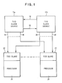
- a dual TOD synchronization system 10 comprised of a pair of identical TOD clock sources 12a and 12b, each of which generates a reference frequency signal.
- the sources are coupled to each other such that the reference frequency generated by one is transmitted to the other.
- the signal generated by source 12a is applied to source 12b via link 14, while the signal from source 12b is coupled to source 12a by link 16.
- the sources 12a and 12b provide respective pluralities of synchronization signals on lines 18 and 20.
- a pair of reference frequency signals, one from each of lines 18 and 20 are transmitted to a common TOD slave 22 associated with one of the processors 24 of the system complex.
- the TOD slaves 22 serve as the TOD clocks in the complex.
- the TOD sources 12a and 12b and the TOD slaves 22 may be coupled to one another by means of dedicated links, as in a dual star configuration, or by a dual redundant bus structure.
- each of the TOD slaves 22 selects one reference frequency signal from the pair of signals transmitted to it by the TOD sources 12a and 12b, and uses such signal to maintain synchronization within the complex.
- the reference frequency signal is a low enough frequency so that any skews between the two clock sources are small with respect to one period of the reference frequency.
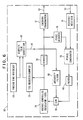
- Fig. 2 provides details of the internal organization of the elements of which TOD clock source 12a of Fig. 1 is comprised. It should be understood that TOD clock source 12b consists of like elements.
- a TOD register/counter 26 which represents a facsimile of the standard format TOD clock utilized by the particular processors in the complex, and as such, it has the same bit resolution as the latter.
- a 64 bit TOD register formal compatible with the IBM S/370 TOD will be assumed.
- the bits of the TOD are numbered from 0 to 63. Bit 0 is the most significant bit and bit 63 is the least.
- the register is a binary counter and is incremented at a rate which causes bit 31 of the register to toggle every 220 microsecond (approximately 1.04 seconds). This is called a mega-micro-second or MuS period.
- a voltage controlled oscillator (VCO) 28 generates the internal clock fo the TOD source 12a.
- This internal clock is used to increment the TOD register/counter 26 and is also divided down in divider 30 to produce the TOD reference frequency for TOD source 12a.
- the period of the reference frequency is selected to be larger than any skews which may appear between sources 12a and 12b due to normal variations in component characteristics.
- the reference frequency is used as a carrier for the data. It should be noted that the actual resolution of the counter (the inherent VCO internal clock frequency) can be arbitrarily high with respect to this reference frequency.
- An encoder/transmitter 32 is provided for encoding and transmitting the TOD source 12a reference frequency, together with other status and data bits.
- a decoder/receiver 34 is provided for receiving and decoding the reference frequency and transmitted data from the other TOD source 12b (Fig. 1).
- phase adjuster 36 Also included in TOD source 12a are phase adjuster 36, phase comparator 38 and filter 40 circuits, and miscellaneous error detection and associated control elements 42.
- the VCO 28 provides an internal clock output signal on line 44 which is used to increment the TOD register/counter 26.
- the signal from the VCO 28 is also applied to divider 30, where it is divided down to produce a reference frequency signal.
- a synchronization point signal or "syncpoint" (the MuS syncpoint in this embodiment) is derived from the count in the TOD register/counter 26, as indicated hereinbefore.
- the reference frequency, syncpoint, and TOD register/counter 26 data and various status indicators are encoded and transmitted by encoder/transmitter 32 to TOD source 12b (Fig. 1) via line 46. As indicated in Fig. 1, all of the last mentioned information is transmitted as well to all of the TOD slave units 22 within the complex.
- the present invention contemplates the use of bi-phase encoding of the data and syncpoint at the reference frequency, with suitable sync, framing and idle symbols.
- the data transmission includes the value of bits 0:31 (high order bits) of the TOD register/counter 26 after the next syncpoint, and further includes various status bits.
- the transmission of the TOD register/counter value is chosen to be well away from the syncpoint transmission, so as to simplify its use at syncpoint with minimally complex control logic.
- the encoded transmission from the other TOD clock source 12b is received by TOD source 12a on line 48 and is applied to decoder/receiver 34, where it is decoded into a reference frequency, syncpoint, and data.
- the data is stored in an appropriate holding register 50 where it is available to the control logic for TOD source 12a.
- phase comparator 38 compares the phases of the two input signals and provides an output signal on line 56 which is the representative of the phase error therebetween.
- a suitable method for performing this phase comparison utilizes a simple exclusive-OR gate with averaging and filtering of its output.
- phase error signal on line 56 is processed utilizing first order lag dynamics with steady state gain K, as is implemented by filter 40.
- the output signal from filter 40 appearing on line 58 is applied to VCO 28, and operates to change its frequency in a direction to cause the phase error signal to approach zero.
- the TOD source 12a includes error detection circuits 42 which monitor the phase error between the incoming reference frequency signal on line 48 and the outgoing signal on line 46 and determines when phase lock is obtained, or when it is lost.
- the error detection circuits also function to detect other simple failures such as power out of regulation and complete loss of the input signal.
- the circuits 42 further provide consistency checks such as the correct number of cycles between syncpoints. These conditions operate to set various status flags which are included in the data being transmitted from a TOD clock source.
- phase of a signal is the integral of its frequency, and the system applies a first order filter to phase differences, it follows from classical control theory that the system as a whole is a second order system. For the whole fault-tolerant system to be stable under all failure modes, it is necessary that the parameters of the first order filter be chosen such that the second order system is overdamped. It should be noted that in stady state operation each of the TOD clock sources 12a and 12b of the duplex system will perceive a steady state phase error which is required to deflect that TOD source's intrinsic operating frequency to the steady state operating frequency. If the propagation delay phase compensation is perfect, this operating frequency will be the average of the two intrinsic operating frequencies.
- the operating frequency will also be partially determined by the magnitude of this error and the steady state gain K.
- the steady state result will be such that the TOD clock sources 12a and 12b are operating at exactly the same frequency but with some steady state phase error or skew between them.
- the maximum magnitude of this phase error can be computed as a function of implementation parameters; and the reference frequency should be such that this maximum steady state phase error is no more than 30 to 45 degrees of the reference frequency. It must be smaller than the performance boundary of the phase comparator being employed and should additionally include, engineering margins.
- the most commonly and economically implemented phase comparators operate over +/-90 degrees, but +/-180 degree comparators are also easily implemented and are within the state of the art.
- the TOD clocks and syncpoint can be aligned by having one of the TOD clock sources accept the TOD value and MuS syncpoint from the other clock source.
- the TOD value could be entered from either TOD clock source through a manual operation or from an external frequency reference standard, and the alternate TOD clock source could simply accept this value.
- one of the TOD clock sources is restarting, such as after repair or power interruption, it would accept the TOD value and syncpoint from the operating TOD source. It should be noted that under normal operating conditions, the two TOD clock sources 12a and 12b will maintain alignment with each other without adjustments of either the TOD value of the MuS syncpoint.
- a clock source should not attempt to realign itself with the other source, except in those cases where it has a positive indication of an internal fault such as a power on reset. It is therefore advantageous that discreet data should be transmitted as part of the data stream between the two TOD clock sources, to indicate whether a source believes that it is maintaining frequency lock, restarting, or other situation and whether it believes that its TOD value and syncpoint are valid.
- the accepting side To accept the syncpoint and TOD value from the other side the accepting side must first establish reference frequency phase lock. Once this is done, the control logic 42 inhibits TOD counter 26 via line 27, clearing those bits of the TOD counter 26 to zero below the syncpoint (bits 32 through 63 in the embodiment).
- control logic 42 waits until data register 50 has received the transmitted TOD value from decoder/receiver 34 for the higher order bits of the TOD counter and loads these via line 29 into the TOD counter above the syncpoint (bits 0 through 31 in the embodiment). The control logic 42 then waits until it receives the next syncpoint signal and reenables the TOD register/counter via line 27 at that syncpoint. At this time, the TOD register/counters are aligned to the skew accuracy of the reference signal.
- circuit elements which comprise the receiver 60 of the TOD slave 22 for the dual redundant broadcast clock embodiment.
- Such elements include the decoder/receiver units 62 and 64 for the pair of broadcast signals transmitted respectively by the TOD clock sources 12a and 12b.
- a phase-locked loop with its associated oscillator 66 is provided for driving a slave TOD register/counter 68.
- error detection and control logic circuits 70 are also included in the receiver circuit organization.
- the reference frequency signals from the TOD clock sources 12a and 12b are received on lines 18 and 20 and are decoded by decoder/receivers 62 and 64 into signals representative of a reference frequency, syncpoint event and data.
- the data is held in registers 72a and 72b for use by the control logic circuits 70.
- Either the reference frequency derived from TOD clock source 12a or clock source 12b is used to drive the TOD slave's phase-locked loop 66 which is coupled to the slave TOD register/counter 68 and increments the latter.
- the TOD clock source which provides the selected reference signal is referred to as the "primary”; the other clock source, "secondary”. It should be noted that the reference frequency on line 74 is too low to directly drive the slave TOD register/counter 68, and thus the slave phase-locked loop 66 is required to frequency multiply the reference frequency to the desired level to obtain the necessary TOD register/counter resolution, in the same fashion as described for the TOD clock source.
- the error detection circuits 70 are utilized to detect obvious failures of either incoming signal on lines 18 or 20, and are effective in switching the TOD slave 22 via select unit 71 to the secondary source when a failure of the primary is observed. Moreover, when the error detection circuits 70 are unable to maintain frequency and phase lock with a signal from either TOD clock source or both signals indicate a failed condition, they post a synchronization exception to the processor.
- the error detection circuits provide as a minimum, detection for complete loss of a signal from a clock source, phase or syncpoint misalignment either between the primary or secondary TOD clock sources and the TOD slave, phase or syncpoint misalignment between the TOD clock sources, and disagreement between the TOD clock sources and/or the slave TOD values.
- Fig. 4 illustrates, by way of example, the failure of the reference frequency signal of clock source 12a at point "A”, and the transfer of TOD slave 22 to the "nearest" reference frequency pulse at point "B", generated within clock source 12b.
- the skew between the reference frequency pulses generated respectively within clock sources 12a and 12b must be small relative to the period of the reference frequency.
- the magnitude of the reference frequency is chosen to be low enough that adjacent reference frequency pulses occur relatively far apart. Accordingly, the transfer of the TOD slave 22 from clock source 12a to source 12b is achieved without any ambiguity as to the pulse from source 12b which is to be accepted by the slave.
- the next pulse from source 12b at point "B" occurring after the failure of source 12a at point “A” is the "correct” pulse from the standpoint of synchronization.
- the incrementation of the TOD slave register/counter 68 by the high frequency internal clock pulses is unaffected by the transfer from one clock source to the other. That is, none of the high frequency internal clock pulses applied to the register/counter 68 are lost in the transfer process.
- the TOD slave's clock and syncpoint can be aligned with one of the reference signals from TOD clock sources 12a or 12b by having it load the TOD bits 0:31, and inhibiting its own internal TOD register/counter 68 incrementation until the syncpoint signal is received.
- this synchronization process is controlled by the SETCLOCK instruction from the processor 24.
- the processor receives a signal on line 63 from select unit 71 to read via line 65a or 65b, the received TOD value from either data register 72a or 72b, containing data derived from the selected reference frequency carrier.
- the processor 24 then loads the data into the TOD slave register/counter 68 via line 67 with a SETCLOCK instruction. This instruction loads the TOD and inhibits the register/counter until a synchronization signal occurs. This signal is provided by the syncpoint signal.
- the alignment procedure should only be executed once during processor initialization, and only in conjunction with the above mentioned programming instruction of the processor. Once alignment is achieved, then a disagreement between the slave's TOD value syncpoint and the transmitted reference signals is an indication of a fault. If the slave's internal TOD value syncpoint differs from the primary TOD clock source reference frequency but agrees with the secondary, then the primary has failed and the slave must switch to the secondary reference. If both reference frequencies from the primary and secondary agree, but the slave's clock disagrees, then the slave's TOD clock should be assumed to have failed, and a synchronization exception must be raised in the processor.
- the TOD slave 22 may switch back and forth from the primary clock source to the secondary source without interfering with the integrity and alignment of its own TOD value. If necessary, the switchover may require a phase alignment of the oscillator in the phase-locked loop 66 and this can be accomplished without disturbing the slave's TOD value.
- the TOD slave 22 may select either one as the primary. Once selected, the slave may always return to this primary source, for example, after it has been taken out of service for a failure and is subsequently restored. It should be observed that the ability to easily switch from one source to the other requires that the sources have only small skews with respect to one another and the reference frequency.
- the error detection circuits 70 are necessary to detect failures in the reference frequency signals from the TOD clock sources. Such circuits may be implemented for example, by a simple monitor responsive to the power for the TOD sources. Thus, a power failure could be used to inhibit transmission of the reference clock frequency from the associated TOD clock source. A total failure of the oscillator in a clock source should have the same results. Other failures may also be easily detected, such an incorrect number of reference cycles between sync signals. Although many different failures may be detected and are generally tolerated by the duplex system, there are certain deficiencies in the system which cannot be detected.
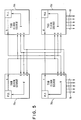
- a solution to the inherent detection and fault isolation problems of a purely dual system requires additional frequency standards. Theory dictates 3f + 1 frequency sources to tolerate all single point failures. A quad implementation is therefore required to tolerate all single point failures. Conveniently, a quad implementation can be constructed which remedies the uncovered fault modes mentioned above, and which is compatible with the described duplex distribution scheme. Such a quad configuration is partitioned and packaged in two pieces creating a dual partition quad architecture. Such a system is illustrated i Fig. 5.
- Fig. 5 depicts four TOD clock sources 76a, 76b, 76c and 76d which are substantially the same as clock source 12a or 12b illustrated in Fig. 2.
- Each of the clock sources has a phase-locked loop (PLL).
- Clock sources 76a, 76b, 76c and 76d transmit respectively reference signals a, b, c and d to each of the other three sources.
- Each TOD clock source then votes (V) the received three signals and attempts to phase lock to the voted reference signal.
- V phase-locked loop
- Any two of the TOD clock sources can then be used to transmit dual reference signals 78 and 80 to the TOD slave 22 as in the case of the duplex system.
- clock sources 76c and 76d may be chosen as primary and secondary sources. Comparison circuits internal to a TOD clock source can easily detect the loss of phase lock by the transmitting source and can provide a failure indication which is easily detected by the TOD slave receiver 60. This detection forces the slave 22 to switch to the secondary source quickly enough to avoid breaking phase lock. It is apparent that except for the elimination of the so called "near correct frequency" failure modes of the purely dual structure of Fig. 1, the quad architecture of Fig. 5 has similar operational characteristics to the duplex structure.
- Fig. 6 illustrates a mechanism for frequency steering a TOD clock source 82 of either the dual or quad configurations.
- a summing circuit 84 is interposed between the filter 40 and oscillator 28. The output of the summing circuit 84 on line 86 is applied to the VCO 28 and controls the output frequency thereof.
- the TOD clock value is stored in the TOD register/counter 26.
- a precise time reference 88 is utilized. The signals from the TOD register/counter 26 and the precise time reference 88 are applied to a compute trim correction circuit 90 where they are compared. Deviations in the frequencies of the compared signals cause the trim correction circuit 90 to generate a steering signal on line 92.
- This signal is applied to an authority filter 94, the function of which is to limit the magnitude of the trim adjustment provided by the steering signal so that it is not so great as to force a break in phase lock among the synchronized components of the system.
- the output of the authority filter 94 is summed with the processed error signal from filter 40 in summing circuit 84.
- the output of the summing circuit 84 will cause the VCO output frequency to be deflected downward or upward.
- the remaining elements of TOD clock source 82 function in the same manner as the like-named numbered of Fig. 2.
- the integrity of synchronization is uncoupled from the accuracy of the TOD clock.
- the steering mechanism need not be continuous since the normal synchronization of the TOD clock source 82 can be adequately maintained for long periods of time without diverging from real time significantly. Accordingly the precise time reference does not need to be continuously available.
- a radio based frequency standard such as WWV could be utilized intermittently, or alternately the precise frequency reference 88 may simply be a fixed frequency oscillator with manual corrections to the time when significant deviations are noted.
- the value of the reference frequency has a significant effect on the encode/transmitter and decode/receiver logic as well as the nature of the distribution of the reference signals. For example, if synchronization requirements dictate skews of less than one microsecond, then a reference frequency near 10 to 100 KHz. is appropriate. Twisted wire distribution of such a low frequency is adequate for star topologies, and coaxial or twinax may be used for buses. On the other hand, skews of less than one microsecond will require more judicious management of cable lengths, as cable propagation delays are significant relative to this skew requirement. If the application allows 10 or 20 microsecond skews, then the reference frequency below 1 KHz and twisted pairs with only coarse management of cable length will be adequate.
Abstract
Description
- A significant aspect of operating a plurality of data processors in a multiprocessor system complex is the synchronization of the individual clocks associated therewith. For example, it is desirable and in fact, frequently necessary that the separate Time of Day (TOD) clocks of the coupled processors be synchronized if these processors are sharing Direct Access Storage Devices (DASD), the data contained upon DASD and other resources, or the processors are exchanging messages. Concomitant with the need for synchronization is that the synchronizing mechanism be fault tolerant. That is, single points of failure in the mechanism itself should be tolerated, such that loss of synchronization in the entire system complex will not occur.
- Considerable effort has been directed by the computer industry to the design of fault-tolerant clock systems. Many of these designs have relied upon primary/secondary configurations of clocks. These systems typically have difficulty in detecting failures on the primary and when problems are detected they cannot easily switch from the primary to the secondary. Attempts to address these problems have been both expensive and unsatisfactory. The root cause of these problems is that the required resolution of the clock is typically smaller than the skew between the primary and secondary clock.
- What is needed is an economical hardware means for providing synchronized operation of arbitrarily high separate resolution TOD clocks in the processors in a system complex. Moreover, since the complex represents a valuable resource and the individual processors exhibit intrinsic isolation of failures to single machines, it is necessary that the chosen clock synchronization mechanism not behave as a coupled or common failure mechanism, whereby a single point of failure therein could bring the entire complex down. The synchronization mechanism of the present invention fills such a need.
- In accordance with the present invention there is provided a fault tolerant synchronization mechanism comprised basically of dual redundant TOD clock synchronization sources, and a plurality of TOD slaves which serve as the TOD clocks in the respective processors of the system complex. Each of the redundant TOD clock sources distributes a TOD synchronization signal to one of the TOD slaves. Thus, each slave receives two synchronization signals. The TOD slaves include means for selecting a valid TOD signal from between the two signals and the slave uses such signal to maintain synchronization within the complex.
- More specifically, the present invention provides an economical means of maintaining synchronism between the two sides of the duplexed TOD clock reference sources. The reference frequency signals, as well as other various status and data bits generated within one side of the TOD sources are encoded and transmitted to the other side of the TOD sources, and vice versa. In a given side, the phase of the incoming reference frequency signal is compared to the phase of the reference signal generated within the given side. A difference in phase between the signals results in a phase error signal which, after suitable processing, is used to vary the given side's reference frequency in a direction to drive the perceived phase error toward zero.
- The present invention also provides an economical means of receiving a duplexed TOD time reference, and for trouble-free switching from one side of the TOD clock sources to the other side, when required for failure accommodation or operational convenience. Accordingly, each TOD slave receives two reference frequency signals from the respective sides of the TOD clock sources, and selects one of them. The selected signal drives a phase locked-loop in the TOD slave. Error detection means associated with the slave, monitor the incoming reference frequency signal. If a failure is detected, the slave is switched to the other incoming reference signal. In the event that frequency and phase lock cannot be maintained with either incoming signal, or both incoming signals have failed, a synchronization exception is raised in the associated processor.
- While the fault coverage provided by the duplex system is adequate for most applications, the present invention contemplates a quad system implementation for near perfect coverage of all single points of failure of the synchronization mechanism. This last implementation is compatible with the duplex distribution of reference frequency signals to each TOD slave as described hereinbefore.
- Finally, although either the dual or quad implementations will produce synchronized TOD clocks of acceptable accuracy for many situations, better conformity to real time may be achieved in accordance with the present invention by frequency steering elements within the TOD clock sources. This procedure involves correction of the generated reference frequency signal by summing predetermined numbers of cycles of the latter signal and comparing the result to a more precise time standard.
- Fig. 1 is a block diagram of the overall dual TOD synchronization system implementation in accordance with the present invention.
- Fig. 2 illustrates the common internal organization of either side of the dual redundant TOD clock sources.
- Fig. 3 depicts the TOD slave receiver circuit organization for the dual redundant clock implementation.
- Fig. 4 is a timing diagram illustrating the relationship of the reference frequency signals generated respectively by the dual clock sources.
- Fig. 5 is a block diagram of a quad TOD synchronization system implementation, which is compatible with the duplex reference frequency distribution mode of Fig. 1.
- Fig. 6 illustrates a mechanism for frequency steering an element of either the dual or quad implementations of Figs. 1 and 5 respectively.
- With reference to Fig. 1, there is shown a dual TOD synchronization system 10 comprised of a pair of identical
TOD clock sources source 12a is applied tosource 12b vialink 14, while the signal fromsource 12b is coupled tosource 12a bylink 16. Additionally, thesources lines lines common TOD slave 22 associated with one of theprocessors 24 of the system complex. The TODslaves 22 serve as the TOD clocks in the complex. TheTOD sources TOD slaves 22 may be coupled to one another by means of dedicated links, as in a dual star configuration, or by a dual redundant bus structure. As will be described in detail hereinafter, each of theTOD slaves 22 selects one reference frequency signal from the pair of signals transmitted to it by theTOD sources - Fig. 2 provides details of the internal organization of the elements of which
TOD clock source 12a of Fig. 1 is comprised. It should be understood thatTOD clock source 12b consists of like elements. - Before describing the operation of the
TOD source 12a, a brief explanation of each of the elements present therein and its function is given. A TOD register/counter 26 is provided which represents a facsimile of the standard format TOD clock utilized by the particular processors in the complex, and as such, it has the same bit resolution as the latter. For purposes of example, a 64 bit TOD register formal compatible with the IBM S/370 TOD will be assumed. The bits of the TOD are numbered from 0 to 63. Bit 0 is the most significant bit andbit 63 is the least. The register is a binary counter and is incremented at a rate which causes bit 31 of the register to toggle every 220 microsecond (approximately 1.04 seconds). This is called a mega-micro-second or MuS period. - A voltage controlled oscillator (VCO) 28 generates the internal clock fo the
TOD source 12a. This internal clock is used to increment the TOD register/counter 26 and is also divided down individer 30 to produce the TOD reference frequency forTOD source 12a. As seen in Fig. 4, the period of the reference frequency is selected to be larger than any skews which may appear betweensources - An encoder/
transmitter 32 is provided for encoding and transmitting theTOD source 12a reference frequency, together with other status and data bits. - A decoder/
receiver 34 is provided for receiving and decoding the reference frequency and transmitted data from theother TOD source 12b (Fig. 1). - Also included in
TOD source 12a arephase adjuster 36,phase comparator 38 andfilter 40 circuits, and miscellaneous error detection and associatedcontrol elements 42. - In operation, the
VCO 28 provides an internal clock output signal online 44 which is used to increment the TOD register/counter 26. The signal from theVCO 28 is also applied todivider 30, where it is divided down to produce a reference frequency signal. A synchronization point signal or "syncpoint" (the MuS syncpoint in this embodiment) is derived from the count in the TOD register/counter 26, as indicated hereinbefore. The reference frequency, syncpoint, and TOD register/counter 26 data and various status indicators are encoded and transmitted by encoder/transmitter 32 toTOD source 12b (Fig. 1) vialine 46. As indicated in Fig. 1, all of the last mentioned information is transmitted as well to all of theTOD slave units 22 within the complex. While various methods of encoding are well known, the present invention contemplates the use of bi-phase encoding of the data and syncpoint at the reference frequency, with suitable sync, framing and idle symbols. The data transmission includes the value of bits 0:31 (high order bits) of the TOD register/counter 26 after the next syncpoint, and further includes various status bits. The transmission of the TOD register/counter value is chosen to be well away from the syncpoint transmission, so as to simplify its use at syncpoint with minimally complex control logic. - The encoded transmission from the other
TOD clock source 12b is received byTOD source 12a online 48 and is applied to decoder/receiver 34, where it is decoded into a reference frequency, syncpoint, and data. The data is stored in anappropriate holding register 50 where it is available to the control logic forTOD source 12a. - The reference frequency signal output of decoder/
receiver 48 is applied vialine 52 to one input of aphase comparator 38. Similarly, the reference frequency signal output fromdivider 30 online 54 is applied to the other input ofphase comparator 38, after it has received a phase adjustment inphase adjuster 36. The phase adjustment is necessary to compensate for the phase shift resulting from transmission propagation delays.Phase comparator 38 compares the phases of the two input signals and provides an output signal online 56 which is the representative of the phase error therebetween. A suitable method for performing this phase comparison utilizes a simple exclusive-OR gate with averaging and filtering of its output. - The phase error signal on
line 56 is processed utilizing first order lag dynamics with steady state gain K, as is implemented byfilter 40. The output signal fromfilter 40 appearing online 58 is applied toVCO 28, and operates to change its frequency in a direction to cause the phase error signal to approach zero. - The
TOD source 12a includeserror detection circuits 42 which monitor the phase error between the incoming reference frequency signal online 48 and the outgoing signal online 46 and determines when phase lock is obtained, or when it is lost. The error detection circuits also function to detect other simple failures such as power out of regulation and complete loss of the input signal. Thecircuits 42 further provide consistency checks such as the correct number of cycles between syncpoints. These conditions operate to set various status flags which are included in the data being transmitted from a TOD clock source. - Since the phase of a signal is the integral of its frequency, and the system applies a first order filter to phase differences, it follows from classical control theory that the system as a whole is a second order system. For the whole fault-tolerant system to be stable under all failure modes, it is necessary that the parameters of the first order filter be chosen such that the second order system is overdamped. It should be noted that in stady state operation each of the
TOD clock sources TOD clock sources - During initialization, and after frequency lock has been achieved between the two
TOD clock sources TOD clock sources control logic 42 inhibitsTOD counter 26 vialine 27, clearing those bits of theTOD counter 26 to zero below the syncpoint (bits 32 through 63 in the embodiment). Then thecontrol logic 42 waits until data register 50 has received the transmitted TOD value from decoder/receiver 34 for the higher order bits of the TOD counter and loads these vialine 29 into the TOD counter above the syncpoint (bits 0 through 31 in the embodiment). Thecontrol logic 42 then waits until it receives the next syncpoint signal and reenables the TOD register/counter vialine 27 at that syncpoint. At this time, the TOD register/counters are aligned to the skew accuracy of the reference signal. - With reference to Fig. 3, there are illustrated the circuit elements which comprise the
receiver 60 of theTOD slave 22 for the dual redundant broadcast clock embodiment. Such elements include the decoder/receiver units TOD clock sources oscillator 66 is provided for driving a slave TOD register/counter 68. Also included in the receiver circuit organization are appropriate error detection andcontrol logic circuits 70. - In operation, the reference frequency signals from the
TOD clock sources lines receivers registers control logic circuits 70. - Either the reference frequency derived from
TOD clock source 12a orclock source 12b is used to drive the TOD slave's phase-lockedloop 66 which is coupled to the slave TOD register/counter 68 and increments the latter. The TOD clock source which provides the selected reference signal is referred to as the "primary"; the other clock source, "secondary". It should be noted that the reference frequency online 74 is too low to directly drive the slave TOD register/counter 68, and thus the slave phase-lockedloop 66 is required to frequency multiply the reference frequency to the desired level to obtain the necessary TOD register/counter resolution, in the same fashion as described for the TOD clock source. - The
error detection circuits 70 are utilized to detect obvious failures of either incoming signal onlines TOD slave 22 via select unit 71 to the secondary source when a failure of the primary is observed. Moreover, when theerror detection circuits 70 are unable to maintain frequency and phase lock with a signal from either TOD clock source or both signals indicate a failed condition, they post a synchronization exception to the processor. The error detection circuits provide as a minimum, detection for complete loss of a signal from a clock source, phase or syncpoint misalignment either between the primary or secondary TOD clock sources and the TOD slave, phase or syncpoint misalignment between the TOD clock sources, and disagreement between the TOD clock sources and/or the slave TOD values. - Fig. 4 illustrates, by way of example, the failure of the reference frequency signal of
clock source 12a at point "A", and the transfer ofTOD slave 22 to the "nearest" reference frequency pulse at point "B", generated withinclock source 12b. As noted hereinbefore, the skew between the reference frequency pulses generated respectively withinclock sources TOD slave 22 fromclock source 12a tosource 12b is achieved without any ambiguity as to the pulse fromsource 12b which is to be accepted by the slave. The next pulse fromsource 12b at point "B" occurring after the failure ofsource 12a at point "A" is the "correct" pulse from the standpoint of synchronization. The incrementation of the TOD slave register/counter 68 by the high frequency internal clock pulses is unaffected by the transfer from one clock source to the other. That is, none of the high frequency internal clock pulses applied to the register/counter 68 are lost in the transfer process. - On the other hand, if the period of the reference frequency had been smaller than the skew between
sources source 12a, would causeslave 22 to pick up the next available pulse fromsource 12b, even though the "correct" pulse is further downstream-displaced in accordance with the inherent skew. While the skew is initially apparent from an examination of adjacent syncpoint signals (MuS) from the respective pair of clock sources, such a reference point is not apparent during operation and theTOD slave 22 is unable to determine which reference frequency pulse to access during transfer. - At start up, the TOD slave's clock and syncpoint can be aligned with one of the reference signals from
TOD clock sources counter 68 incrementation until the syncpoint signal is received. In the proposed embodiment for an IBM system 370 this synchronization process is controlled by the SETCLOCK instruction from theprocessor 24. Thus, the processor receives a signal online 63 from select unit 71 to read vialine processor 24 then loads the data into the TOD slave register/counter 68 vialine 67 with a SETCLOCK instruction. This instruction loads the TOD and inhibits the register/counter until a synchronization signal occurs. This signal is provided by the syncpoint signal. - The alignment procedure should only be executed once during processor initialization, and only in conjunction with the above mentioned programming instruction of the processor. Once alignment is achieved, then a disagreement between the slave's TOD value syncpoint and the transmitted reference signals is an indication of a fault. If the slave's internal TOD value syncpoint differs from the primary TOD clock source reference frequency but agrees with the secondary, then the primary has failed and the slave must switch to the secondary reference. If both reference frequencies from the primary and secondary agree, but the slave's clock disagrees, then the slave's TOD clock should be assumed to have failed, and a synchronization exception must be raised in the processor.
- The
TOD slave 22 may switch back and forth from the primary clock source to the secondary source without interfering with the integrity and alignment of its own TOD value. If necessary, the switchover may require a phase alignment of the oscillator in the phase-lockedloop 66 and this can be accomplished without disturbing the slave's TOD value. When both of theTOD clock sources TOD slave 22 may select either one as the primary. Once selected, the slave may always return to this primary source, for example, after it has been taken out of service for a failure and is subsequently restored. It should be observed that the ability to easily switch from one source to the other requires that the sources have only small skews with respect to one another and the reference frequency. - As noted hereinbefore, the
error detection circuits 70 are necessary to detect failures in the reference frequency signals from the TOD clock sources. Such circuits may be implemented for example, by a simple monitor responsive to the power for the TOD sources. Thus, a power failure could be used to inhibit transmission of the reference clock frequency from the associated TOD clock source. A total failure of the oscillator in a clock source should have the same results. Other failures may also be easily detected, such an incorrect number of reference cycles between sync signals. Although many different failures may be detected and are generally tolerated by the duplex system, there are certain deficiencies in the system which cannot be detected. For example, if the oscillator frequency is "nearly correct", or the twoTOD clock sources - A solution to the inherent detection and fault isolation problems of a purely dual system requires additional frequency standards. Theory dictates 3f + 1 frequency sources to tolerate all single point failures. A quad implementation is therefore required to tolerate all single point failures. Conveniently, a quad implementation can be constructed which remedies the uncovered fault modes mentioned above, and which is compatible with the described duplex distribution scheme. Such a quad configuration is partitioned and packaged in two pieces creating a dual partition quad architecture. Such a system is illustrated i Fig. 5.
- Fig. 5 depicts four
TOD clock sources clock source Clock sources TOD slave 22 as in the case of the duplex system. For compatibility with the dual philosophy described hereinbefore,clock sources TOD slave receiver 60. This detection forces theslave 22 to switch to the secondary source quickly enough to avoid breaking phase lock. It is apparent that except for the elimination of the so called "near correct frequency" failure modes of the purely dual structure of Fig. 1, the quad architecture of Fig. 5 has similar operational characteristics to the duplex structure. - Actual operative embodiments of the duplex and quad structures have produced synchronized TOD clocks which are accurate to approximately one second per day. This degree of accuracy is entirely suitable for many situations. However, applications exist in which better conformity to real time is desirable or even required. The present invention contemplates this increased accuracy as being best achieved by employing frequency steering with the TOD clock sources. Fig. 6 illustrates a mechanism for frequency steering a
TOD clock source 82 of either the dual or quad configurations. - A comparison of Fig. 6 with the internal organization of the TOD clock source of Fig. 2, reveals the presence of the additional elements. A summing
circuit 84 is interposed between thefilter 40 andoscillator 28. The output of the summingcircuit 84 on line 86 is applied to theVCO 28 and controls the output frequency thereof. The TOD clock value is stored in the TOD register/counter 26. Aprecise time reference 88 is utilized. The signals from the TOD register/counter 26 and theprecise time reference 88 are applied to a computetrim correction circuit 90 where they are compared. Deviations in the frequencies of the compared signals cause thetrim correction circuit 90 to generate a steering signal online 92. This signal is applied to anauthority filter 94, the function of which is to limit the magnitude of the trim adjustment provided by the steering signal so that it is not so great as to force a break in phase lock among the synchronized components of the system. The output of theauthority filter 94 is summed with the processed error signal fromfilter 40 in summingcircuit 84. Depending upon the nature of the steerng signal, that is whether the reference frequency time is observed to be fast or slow, the output of the summingcircuit 84 will cause the VCO output frequency to be deflected downward or upward. The remaining elements ofTOD clock source 82 function in the same manner as the like-named numbered of Fig. 2. - It should be noted that in the frequency steering scheme of Fig. 6, the integrity of synchronization is uncoupled from the accuracy of the TOD clock. The steering mechanism need not be continuous since the normal synchronization of the
TOD clock source 82 can be adequately maintained for long periods of time without diverging from real time significantly. Accordingly the precise time reference does not need to be continuously available. A radio based frequency standard such as WWV could be utilized intermittently, or alternately theprecise frequency reference 88 may simply be a fixed frequency oscillator with manual corrections to the time when significant deviations are noted. - Actual operative embodiments of both the dual and quad configurations have been constructed using VDO's single chip controllers and discreet phase measurement circuits. The controller chips were used to digitally implement the necessary phase voting and filtering. Additional circuits consist of simple dividers, counters and control circuits. The voting circuit used in the quad implementation may be provided by a majority logic. Both the TOD clock sources and the receiver of the TOD slaves may be mechanized with other circuit elements well known to the electronic circuit designer.
- It should be noted that the value of the reference frequency has a significant effect on the encode/transmitter and decode/receiver logic as well as the nature of the distribution of the reference signals. For example, if synchronization requirements dictate skews of less than one microsecond, then a reference frequency near 10 to 100 KHz. is appropriate. Twisted wire distribution of such a low frequency is adequate for star topologies, and coaxial or twinax may be used for buses. On the other hand, skews of less than one microsecond will require more judicious management of cable lengths, as cable propagation delays are significant relative to this skew requirement. If the application allows 10 or 20 microsecond skews, then the reference frequency below 1 KHz and twisted pairs with only coarse management of cable length will be adequate.
- In conclusion, there has been disclosed an economical and effective means for providing fault- tolerant hardware synchronized operation of the separate clocks of a multiprocessor system. While particular circuit parameters have been mentioned relative to the synchronization implementations, it should be understood that such information has been presented solely for purpose of example.
Claims (13)
at least a pair of like TOD clock sources (12a, 12b) disposed in a duplex configuration, each of said clock sources including;
means (28) for generating an internal clock signal having a predetermined frequency,
a TOD register/counter (26) having a plurality of bits and being coupled to said generating means, said internal clock signal being applied to said register/counter for incrementing the latter at the rate of said predetermined frequency, said register/counter storing data representative of the TOD clock value, the switching of a predetermined bit in said register/counter providing a syncpoint signal,
means (30) coupled to said generating means for dividing said predetermiend frequency to provide a lower reference frequency signal for synchronization purposes,
means (32) coupled in common to said dividing means and to said register/counter for transmitting said reference frequency signal to the other of said TOD clock sources, said reference frequency signal serving as a carrier for transmitting information including said syncpoint signal and said TOD clock value data to said other of said clock sources, and
means (34) for receiving said reference frequency signal and said information from said other of said clock sources.
means (40) for applying said error signal to said generating means (28) to change said predetermined frequency and the reference frequency signal derived therefrom in a direction to cause said error signal to approach zero.
a holding register (50) coupled to said decoder/receiver means (34) for storing said data.
a first control logic means for inhibiting the incrementation of a first register/counter in a first of said clock sources which is to be aligned with a second register/counter in a second of said clock sources,
said first control logic means clearing the lower order bits of said first register/counter which are below said predetermined bit associated with said syncpoint signal,
said first control logic means reading the higher order bits received from said second register/counter which are above said predetermined bit and are stored in said holding register of said first clock source, into said first register/counter,
said first control logic means being responsive to the occurrence of the next syncpoint signal from said second clock source to reenable said first register/counter, thereby placing said first and second register/counters into substantial alignment.
a precise time reference,
a compute trim correction means having a pair of input terminals and an output terminal,
means for coupling signals from said precise time reference and said TOD register/counter respectively to said pair of input terminals of said compute trim correction means, said compute trim correction means comparing the last mentioned signals and generating a steering signal on its output terminal proportional to the difference in the frequencies of said last mentioned signals,
sum means having a pair of input terminals and an output terminal,
authority filter means interposed between said output terminal of said compute trim correction means and one of said pair of input terminals of said sum means, said authority filter means limiting the magnitude of said steering signal so as to preclude a break in phase lock in said clock source,
said processed error signal from said filter means being applied to the other input terminal of said sum means,
the output terminal of said sum means being coupled to said input terminal of said generating means, the resultant signal from said sum means appearing on said output terminal thereof and causing the frequency of said generating means to tend to conform to the frequency of said precise time reference.
a plurality of TOD slaves (22) associated respectively with the processors (24) of said complex,
said pair of TOD clock sources (12a, 12b) transmitting respectively said reference frequency signals to each of said TOD slaves,
each of said TOD slaves having a pair of decoder/receivers (62, 64) for receiving respectfully said reference frequency signals from said pair of TOD clock sources,
means (71) for selecting one of said reference frequency signals, and
means (66, 68) responsive to the selected reference frequency signal for providing a TOD clock for use by its associated processor.
error detection means operatively coupled to both said reference frequency signals for monitoring the status thereof,
signal select means coupled to said error detection means and responsive thereto for selectively coupling said means for providing said TOD clock, to one of said reference frequency signals,
the detection of a failure in the reference frequency signal coupled to a TOD slave at any given time by said error detection means causing said signal select means to switch said means for providing said TOD clock to the other of said reference frequency signals, thereby preventing loss of synchronization in said multiprocessor complex.
a slave TOD register/counter (68) coupled to said oscillator for storing the value of said TOD clock, said oscillator incrementing said slave TOD register/counter at a predetermined rate,
said signal select means (71) being coupled to said oscillator whereby said oscillator is driven by said selected one of said pair of reference frequency signals transmitted by said clock sources to said decoder/receiver of each of said TOD slaves (12a, 12b).
first and second pairs of like TOD clock sources (76a, 76b, 76c, 76d) disposed in a quad configuration which is substantially immune to all single point failures, each of said clock sources including,
means disposed in a phase-locked loop for generating an internal clock signal having a predetermined frequency,
a TOD register/counter having a plurality of bits and being coupled to said generating means, said internal clock signal being applied to said register/counter for incrementing the latter at the rate of said predetermined frequency, said register/counter storing data representative of the TOD clock value, the switching of a predetermined bit in said register/counter providing a syncpoint signal,
means coupled to said generating means for dividing said predetermined frequency to provide lower reference frequency signal for synchronization purposes,
means coupled in common to said dividing means and to said register/counter for transmitting said reference frequency signal to each of the remaining three clock sources, said reference frequency signal serving as a carrier for transmitting information including said syncpoint signal and said TOD clock value data to said three clock sources, and
means for receiving reference frequency signals respectively from said three clock sources,
voting means for selecting one of the three reference frequency signals received thereby, and
means for applying the selected received reference frequency signal to said generating means whereby the respective phases of said transmitted reference frequency signal and said selected received reference frequency signal are brought to substantial agreement.
a plurality of TOD slaves associated respectively with the processors of said complex,
a selected pair of said first and second pairs of TOD clock sources transmitting reference frequency signals to each of said TOD slaves,
each TOD slave including means for receiving the pair of reference frequency signals and for selecting one of them,
each TOD slave further including means responsive to the selected reference frequency signal for providing a TOD clock for use by its associated processor.
Applications Claiming Priority (2)
| Application Number | Priority Date | Filing Date | Title |
|---|---|---|---|
| US26241688A | 1988-10-25 | 1988-10-25 | |
| US262416 | 1988-10-25 |
Publications (3)
| Publication Number | Publication Date |
|---|---|
| EP0365819A2 true EP0365819A2 (en) | 1990-05-02 |
| EP0365819A3 EP0365819A3 (en) | 1991-09-18 |
| EP0365819B1 EP0365819B1 (en) | 1995-08-16 |
Family
ID=22997411
Family Applications (1)
| Application Number | Title | Priority Date | Filing Date |
|---|---|---|---|
| EP89117154A Expired - Lifetime EP0365819B1 (en) | 1988-10-25 | 1989-09-16 | Synchronized fault tolerant clocks for multiprocessor systems |
Country Status (4)
| Country | Link |
|---|---|
| US (1) | US5146585A (en) |
| EP (1) | EP0365819B1 (en) |
| JP (1) | JPH0797328B2 (en) |
| DE (1) | DE68923845T2 (en) |
Cited By (6)
| Publication number | Priority date | Publication date | Assignee | Title |
|---|---|---|---|---|
| EP0461749A2 (en) * | 1990-06-12 | 1991-12-18 | International Business Machines Corporation | Method and apparatus for controlling a variable frequency controlled oscillator |
| EP0800136A1 (en) * | 1996-04-03 | 1997-10-08 | Industrial Control Services Technology Limited | Fault tolerant clock signal source for triplicated data processing system |
| GB2313528A (en) * | 1996-05-21 | 1997-11-26 | Samsung Electronics Co Ltd | Redundant clock system prevents changeover glitches, eg for ATM cells |
| US6195758B1 (en) | 1995-09-29 | 2001-02-27 | Telefonaktiebolaget Lm Ericsson | Operation and maintenance of clock distribution networks having redundancy |
| US6310895B1 (en) | 1995-09-29 | 2001-10-30 | Telefonaktiebolaget Lm Ericsson (Publ) | Clock selector system |
| US6711693B1 (en) * | 2000-08-31 | 2004-03-23 | Hewlett-Packard Development Company, L.P. | Method for synchronizing plurality of time of year clocks in partitioned plurality of processors where each partition having a microprocessor configured as a multiprocessor backplane manager |
Families Citing this family (78)
| Publication number | Priority date | Publication date | Assignee | Title |
|---|---|---|---|---|
| US5504878A (en) * | 1991-02-04 | 1996-04-02 | International Business Machines Corporation | Method and apparatus for synchronizing plural time-of-day (TOD) clocks with a central TOD reference over non-dedicated serial links using an on-time event (OTE) character |
| US5636373A (en) * | 1991-09-04 | 1997-06-03 | International Business Machines Corporation | System for synchronizing logical clock in logical partition of host processor with external time source by combining clock adjustment value with specific value of partition |
| US5544180A (en) * | 1992-06-08 | 1996-08-06 | Qlogic Corporation | Error-tolerant byte synchronization recovery scheme |
| US5327468A (en) * | 1992-06-19 | 1994-07-05 | Westinghouse Electric Corp. | Synchronization of time-of-day clocks in a distributed processing network system |
| US5347227A (en) * | 1992-12-10 | 1994-09-13 | At&T Bell Laboratories | Clock phase adjustment between duplicated clock circuits |
| US5838894A (en) * | 1992-12-17 | 1998-11-17 | Tandem Computers Incorporated | Logical, fail-functional, dual central processor units formed from three processor units |
| JPH06195147A (en) * | 1992-12-23 | 1994-07-15 | Fujitsu Ltd | Clock contrller |
| US5870427A (en) * | 1993-04-14 | 1999-02-09 | Qualcomm Incorporated | Method for multi-mode handoff using preliminary time alignment of a mobile station operating in analog mode |
| US5509035A (en) * | 1993-04-14 | 1996-04-16 | Qualcomm Incorporated | Mobile station operating in an analog mode and for subsequent handoff to another system |
| SE501156C2 (en) * | 1993-04-21 | 1994-11-28 | Ellemtel Utvecklings Ab | Reference signal composed of clock signal and synchronization signal, synchronization device and method, etc. reference signal |
| US5600822A (en) * | 1994-04-05 | 1997-02-04 | International Business Machines Corporation | Resource allocation synchronization in a parallel processing system |
| US5450458A (en) * | 1994-08-05 | 1995-09-12 | International Business Machines Corporation | Method and apparatus for phase-aligned multiple frequency synthesizer with synchronization window decoder |
| US5537583A (en) * | 1994-10-11 | 1996-07-16 | The Boeing Company | Method and apparatus for a fault tolerant clock with dynamic reconfiguration |
| US5758132A (en) * | 1995-03-29 | 1998-05-26 | Telefonaktiebolaget Lm Ericsson | Clock control system and method using circuitry operating at lower clock frequency for selecting and synchronizing the switching of higher frequency clock signals |
| US5742907A (en) * | 1995-07-19 | 1998-04-21 | Ericsson Inc. | Automatic clear voice and land-line backup alignment for simulcast system |
| US5887146A (en) * | 1995-08-14 | 1999-03-23 | Data General Corporation | Symmetric multiprocessing computer with non-uniform memory access architecture |
| US5809540A (en) * | 1995-12-04 | 1998-09-15 | Unisys Corporation | Processor command for prompting a storage controller to write a day clock value to specified memory location |
| US5617375A (en) * | 1995-12-04 | 1997-04-01 | Unisys Corporation | Dayclock carry and compare tree |
| US5631933A (en) * | 1996-02-21 | 1997-05-20 | Hewlett-Packard Company | Phase-locked digital synthesizers |
| US6141769A (en) | 1996-05-16 | 2000-10-31 | Resilience Corporation | Triple modular redundant computer system and associated method |
| US5875320A (en) * | 1997-03-24 | 1999-02-23 | International Business Machines Corporation | System and method for synchronizing plural processor clocks in a multiprocessor system |
| US5925107A (en) * | 1997-04-08 | 1999-07-20 | International Business Machines Corporation | Verifying a time-of-day counter |
| US6003091A (en) * | 1997-04-08 | 1999-12-14 | International Business Machines Corporation | Verifying a time-of-day counter |
| KR100237545B1 (en) * | 1997-06-24 | 2000-01-15 | 김영환 | Time and frequency generating device in cdma system |
| US6163550A (en) * | 1997-11-17 | 2000-12-19 | Qlogic Corporation | State dependent synchronization circuit which synchronizes leading and trailing edges of asynchronous input pulses |
| US6055285A (en) * | 1997-11-17 | 2000-04-25 | Qlogic Corporation | Synchronization circuit for transferring pointer between two asynchronous circuits |
| JPH11346145A (en) * | 1998-05-29 | 1999-12-14 | Nec Corp | Circuit and method for polyphase clock generation |
| US6223228B1 (en) * | 1998-09-17 | 2001-04-24 | Bull Hn Information Systems Inc. | Apparatus for synchronizing multiple processors in a data processing system |
| US6121816A (en) * | 1999-04-23 | 2000-09-19 | Semtech Corporation | Slave clock generation system and method for synchronous telecommunications networks |
| US6631483B1 (en) * | 1999-06-08 | 2003-10-07 | Cisco Technology, Inc. | Clock synchronization and fault protection for a telecommunications device |
| US7350116B1 (en) | 1999-06-08 | 2008-03-25 | Cisco Technology, Inc. | Clock synchronization and fault protection for a telecommunications device |
| US6801951B1 (en) | 1999-10-08 | 2004-10-05 | Honeywell International Inc. | System and method for fault-tolerant clock synchronization using interactive convergence |
| DE10023166A1 (en) * | 2000-05-11 | 2001-11-15 | Alcatel Sa | Multi-computer system for generating a master clock to synchronize a cluster of computers forms a real-time system requiring the master clock to fix the system's cycle time. |
| US7571359B2 (en) * | 2000-07-31 | 2009-08-04 | Massachusetts Institute Of Technology | Clock distribution circuits and methods of operating same that use multiple clock circuits connected by phase detector circuits to generate and synchronize local clock signals |
| US6760764B1 (en) * | 2000-08-09 | 2004-07-06 | Alcatel Canada Inc. | Real time stamp distribution |
| US7324857B2 (en) * | 2002-04-19 | 2008-01-29 | Gateway Inc. | Method to synchronize playback of multicast audio streams on a local network |
| US7333519B2 (en) * | 2002-04-23 | 2008-02-19 | Gateway Inc. | Method of manually fine tuning audio synchronization of a home network |
| US7392102B2 (en) * | 2002-04-23 | 2008-06-24 | Gateway Inc. | Method of synchronizing the playback of a digital audio broadcast using an audio waveform sample |
| US7209795B2 (en) | 2002-04-23 | 2007-04-24 | Gateway Inc. | Method of synchronizing the playback of a digital audio broadcast by inserting a control track pulse |
| US7111228B1 (en) | 2002-05-07 | 2006-09-19 | Marvell International Ltd. | System and method for performing parity checks in disk storage system |
| US7287102B1 (en) | 2003-01-31 | 2007-10-23 | Marvell International Ltd. | System and method for concatenating data |
| US7007114B1 (en) | 2003-01-31 | 2006-02-28 | Qlogic Corporation | System and method for padding data blocks and/or removing padding from data blocks in storage controllers |
| US7219182B2 (en) | 2003-03-10 | 2007-05-15 | Marvell International Ltd. | Method and system for using an external bus controller in embedded disk controllers |
| US7064915B1 (en) | 2003-03-10 | 2006-06-20 | Marvell International Ltd. | Method and system for collecting servo field data from programmable devices in embedded disk controllers |
| US7039771B1 (en) | 2003-03-10 | 2006-05-02 | Marvell International Ltd. | Method and system for supporting multiple external serial port devices using a serial port controller in embedded disk controllers |
| US7492545B1 (en) | 2003-03-10 | 2009-02-17 | Marvell International Ltd. | Method and system for automatic time base adjustment for disk drive servo controllers |
| US7870346B2 (en) | 2003-03-10 | 2011-01-11 | Marvell International Ltd. | Servo controller interface module for embedded disk controllers |
| WO2004105278A1 (en) * | 2003-05-20 | 2004-12-02 | Philips Intellectual Property & Standards Gmbh | Time-triggered communication system and method for the synchronization of a dual-channel network |
| US6970045B1 (en) | 2003-06-25 | 2005-11-29 | Nel Frequency Controls, Inc. | Redundant clock module |
| US7526691B1 (en) | 2003-10-15 | 2009-04-28 | Marvell International Ltd. | System and method for using TAP controllers |
| US8014378B1 (en) | 2003-10-23 | 2011-09-06 | Itt Manufacturing Enterprise, Inc. | Method and apparatus for automatic control of time-of-day synchronization and merging of networks |
| US7716512B1 (en) * | 2004-01-09 | 2010-05-11 | Conexant Systems, Inc. | Real time clock content validation |
| US7139150B2 (en) | 2004-02-10 | 2006-11-21 | Marvell International Ltd. | Method and system for head position control in embedded disk drive controllers |
| US20060020852A1 (en) * | 2004-03-30 | 2006-01-26 | Bernick David L | Method and system of servicing asynchronous interrupts in multiple processors executing a user program |
| US20050240806A1 (en) * | 2004-03-30 | 2005-10-27 | Hewlett-Packard Development Company, L.P. | Diagnostic memory dump method in a redundant processor |
| US7120084B2 (en) | 2004-06-14 | 2006-10-10 | Marvell International Ltd. | Integrated memory controller |
| US8166217B2 (en) | 2004-06-28 | 2012-04-24 | Marvell International Ltd. | System and method for reading and writing data using storage controllers |
| US9201599B2 (en) | 2004-07-19 | 2015-12-01 | Marvell International Ltd. | System and method for transmitting data in storage controllers |
| US8032674B2 (en) | 2004-07-19 | 2011-10-04 | Marvell International Ltd. | System and method for controlling buffer memory overflow and underflow conditions in storage controllers |
| US7757009B2 (en) | 2004-07-19 | 2010-07-13 | Marvell International Ltd. | Storage controllers with dynamic WWN storage modules and methods for managing data and connections between a host and a storage device |
| US7308605B2 (en) * | 2004-07-20 | 2007-12-11 | Hewlett-Packard Development Company, L.P. | Latent error detection |
| US8230252B2 (en) * | 2004-07-20 | 2012-07-24 | Hewlett-Packard Development Company, L.P. | Time of day response |
| US7386661B2 (en) | 2004-10-13 | 2008-06-10 | Marvell International Ltd. | Power save module for storage controllers |
| US7240267B2 (en) | 2004-11-08 | 2007-07-03 | Marvell International Ltd. | System and method for conducting BIST operations |
| US7802026B2 (en) | 2004-11-15 | 2010-09-21 | Marvell International Ltd. | Method and system for processing frames in storage controllers |
| US7330488B2 (en) * | 2004-12-17 | 2008-02-12 | International Business Machines Corporation | System, method, and article of manufacture for synchronizing time of day clocks on first and second computers |
| US7487377B2 (en) * | 2005-02-09 | 2009-02-03 | International Business Machines Corporation | Method and apparatus for fault tolerant time synchronization mechanism in a scaleable multi-processor computer |
| FR2882207B1 (en) * | 2005-02-15 | 2007-04-27 | Alcatel Sa | CLOCK SIGNAL REDUNDANCY SYNCHRONIZATION DEVICE FOR EQUIPMENT OF A SYNCHRONOUS TRANSPORT NETWORK |
| US7609468B2 (en) | 2005-04-06 | 2009-10-27 | Marvell International Ltd. | Method and system for read gate timing control for storage controllers |
| US7721133B2 (en) * | 2006-04-27 | 2010-05-18 | Hewlett-Packard Development Company, L.P. | Systems and methods of synchronizing reference frequencies |
| DE102006048379B4 (en) * | 2006-10-12 | 2008-11-06 | Infineon Technologies Ag | Method for throughput control of an electronic circuit and corresponding throughput control and associated semiconductor circuit |
| US8462907B2 (en) * | 2009-11-10 | 2013-06-11 | Futurewei Technologies, Inc. | Method and apparatus to reduce wander for network timing reference distribution |
| EP2774336B1 (en) * | 2011-11-04 | 2020-01-08 | NXP USA, Inc. | Real-time distributed network module, real-time distributed network and method therefor |
| US9319029B1 (en) | 2015-06-19 | 2016-04-19 | Clover Network, Inc. | System and method for automatic filter tuning |
| US10778360B1 (en) | 2018-12-06 | 2020-09-15 | Xilinx, Inc. | High accuracy timestamp support |
| CN110690894B (en) * | 2019-09-20 | 2023-05-12 | 上海励驰半导体有限公司 | Clock failure safety protection method and circuit |
| CN113767340A (en) * | 2021-08-02 | 2021-12-07 | 华为技术有限公司 | Control device, electronic control system, and vehicle |
| US11940836B2 (en) | 2022-03-31 | 2024-03-26 | International Business Machines Corporation | Dual chip clock synchronization |
Citations (3)
| Publication number | Priority date | Publication date | Assignee | Title |
|---|---|---|---|---|
| US3761884A (en) * | 1970-11-20 | 1973-09-25 | Ericsson Telefon Ab L M | Arrangement for synchronizing a number of co-operating computers |
| GB2000651A (en) * | 1977-06-30 | 1979-01-10 | Int Standard Electric Corp | Master clock arrangement |
| EP0135764A2 (en) * | 1983-08-31 | 1985-04-03 | International Business Machines Corporation | Synchronization of clocks in a distributed computing network |
Family Cites Families (31)
| Publication number | Priority date | Publication date | Assignee | Title |
|---|---|---|---|---|
| US3932847A (en) * | 1973-11-06 | 1976-01-13 | International Business Machines Corporation | Time-of-day clock synchronization among multiple processing units |
| JPS5620746Y2 (en) * | 1974-07-04 | 1981-05-16 | ||
| US4021784A (en) * | 1976-03-12 | 1977-05-03 | Sperry Rand Corporation | Clock synchronization system |
| US4063078A (en) * | 1976-06-30 | 1977-12-13 | International Business Machines Corporation | Clock generation network for level sensitive logic system |
| US4228496A (en) * | 1976-09-07 | 1980-10-14 | Tandem Computers Incorporated | Multiprocessor system |
| US4239982A (en) * | 1978-06-14 | 1980-12-16 | The Charles Stark Draper Laboratory, Inc. | Fault-tolerant clock system |
| US4253144A (en) * | 1978-12-21 | 1981-02-24 | Burroughs Corporation | Multi-processor communication network |
| US4405899A (en) * | 1979-03-01 | 1983-09-20 | Motorola, Inc. | High pass filter and method of making same |
| US4282493A (en) * | 1979-07-02 | 1981-08-04 | Motorola, Inc. | Redundant clock signal generating circuitry |
| US4413318A (en) * | 1980-11-20 | 1983-11-01 | International Business Machines Corporation | Use of nodes to uniquely identify processes |
| US4503490A (en) * | 1981-06-10 | 1985-03-05 | At&T Bell Laboratories | Distributed timing system |
| US4388688A (en) * | 1981-11-10 | 1983-06-14 | International Business Machines Corp. | Shared TOD clock modification bit |
| US4412342A (en) * | 1981-12-18 | 1983-10-25 | Gte Automatic Electric Labs Inc. | Clock synchronization system |
| DE3227848A1 (en) * | 1982-07-26 | 1984-01-26 | Siemens AG, 1000 Berlin und 8000 München | CIRCUIT FOR CLOCK GENERATION IN TELECOMMUNICATION SYSTEMS, IN PARTICULAR TIME MULTIPLEX-DIGITAL SWITCHING SYSTEMS |
| NL8203921A (en) * | 1982-10-11 | 1984-05-01 | Philips Nv | MULTIPLE REDUNDANT CLOCK SYSTEM, CONTAINING A NUMBER OF SYNCHRONIZING CLOCKS, AND CLOCK CIRCUIT FOR USE IN SUCH A CLOCK SYSTEM. |
| US4497022A (en) * | 1982-10-19 | 1985-01-29 | International Business Machines Corporation | Method and apparatus for measurements of channel operation |
| JPS59125192A (en) * | 1983-01-04 | 1984-07-19 | Nec Corp | Clock supply circuit of decentralized control type electronic exchange |
| US4644498A (en) * | 1983-04-04 | 1987-02-17 | General Electric Company | Fault-tolerant real time clock |
| US4577272A (en) * | 1983-06-27 | 1986-03-18 | E-Systems, Inc. | Fault tolerant and load sharing processing system |
| US4554659A (en) * | 1983-12-12 | 1985-11-19 | At&T Bell Laboratories | Data communication network |
| US4569017A (en) * | 1983-12-22 | 1986-02-04 | Gte Automatic Electric Incorporated | Duplex central processing unit synchronization circuit |
| US4575848A (en) * | 1984-02-01 | 1986-03-11 | Westinghouse Electric Corp. | Methods and apparatus for correcting a software clock from an accurate clock |
| US4589066A (en) * | 1984-05-31 | 1986-05-13 | General Electric Company | Fault tolerant, frame synchronization for multiple processor systems |
| US4780892A (en) * | 1984-10-05 | 1988-10-25 | Willi Studer Ag | Scanning frequency synchronization method and apparatus |
| US4709347A (en) * | 1984-12-17 | 1987-11-24 | Honeywell Inc. | Method and apparatus for synchronizing the timing subsystems of the physical modules of a local area network |
| US4667328A (en) * | 1985-04-29 | 1987-05-19 | Mieczyslaw Mirowski | Clocking circuit with back-up clock source |
| US4803708A (en) * | 1986-09-11 | 1989-02-07 | Nec Corporation | Time-of-day coincidence system |
| US5041966A (en) * | 1987-10-06 | 1991-08-20 | Nec Corporation | Partially distributed method for clock synchronization |
| US4864574A (en) * | 1988-02-04 | 1989-09-05 | Rockwell International Corporation | Injection lock clock detection apparatus |
| US4839907A (en) * | 1988-02-26 | 1989-06-13 | American Telephone And Telegraph Company, At&T Bell Laboratories | Clock skew correction arrangement |
| US5041798A (en) * | 1990-06-12 | 1991-08-20 | International Business Machines Corporation | Time reference with proportional steering |
-
1989
- 1989-09-06 JP JP1229476A patent/JPH0797328B2/en not_active Expired - Lifetime
- 1989-09-16 EP EP89117154A patent/EP0365819B1/en not_active Expired - Lifetime
- 1989-09-16 DE DE68923845T patent/DE68923845T2/en not_active Expired - Fee Related
-
1990
- 1990-11-05 US US07/610,336 patent/US5146585A/en not_active Expired - Fee Related
Patent Citations (3)
| Publication number | Priority date | Publication date | Assignee | Title |
|---|---|---|---|---|
| US3761884A (en) * | 1970-11-20 | 1973-09-25 | Ericsson Telefon Ab L M | Arrangement for synchronizing a number of co-operating computers |
| GB2000651A (en) * | 1977-06-30 | 1979-01-10 | Int Standard Electric Corp | Master clock arrangement |
| EP0135764A2 (en) * | 1983-08-31 | 1985-04-03 | International Business Machines Corporation | Synchronization of clocks in a distributed computing network |
Non-Patent Citations (1)
| Title |
|---|
| IBM System/370 Principles of Operation, page 4-23 - 4-29, 1984, IBM * |
Cited By (8)
| Publication number | Priority date | Publication date | Assignee | Title |
|---|---|---|---|---|
| EP0461749A2 (en) * | 1990-06-12 | 1991-12-18 | International Business Machines Corporation | Method and apparatus for controlling a variable frequency controlled oscillator |
| EP0461749A3 (en) * | 1990-06-12 | 1992-09-02 | International Business Machines Corporation | Method and apparatus for controlling a variable frequency controlled oscillator |
| US6195758B1 (en) | 1995-09-29 | 2001-02-27 | Telefonaktiebolaget Lm Ericsson | Operation and maintenance of clock distribution networks having redundancy |
| US6310895B1 (en) | 1995-09-29 | 2001-10-30 | Telefonaktiebolaget Lm Ericsson (Publ) | Clock selector system |
| EP0800136A1 (en) * | 1996-04-03 | 1997-10-08 | Industrial Control Services Technology Limited | Fault tolerant clock signal source for triplicated data processing system |
| GB2313528A (en) * | 1996-05-21 | 1997-11-26 | Samsung Electronics Co Ltd | Redundant clock system prevents changeover glitches, eg for ATM cells |
| GB2313528B (en) * | 1996-05-21 | 1999-07-14 | Samsung Electronics Co Ltd | Apparatus and method of preventing cell data loss during clockwitching |
| US6711693B1 (en) * | 2000-08-31 | 2004-03-23 | Hewlett-Packard Development Company, L.P. | Method for synchronizing plurality of time of year clocks in partitioned plurality of processors where each partition having a microprocessor configured as a multiprocessor backplane manager |
Also Published As
| Publication number | Publication date |
|---|---|
| JPH02128232A (en) | 1990-05-16 |
| DE68923845D1 (en) | 1995-09-21 |
| EP0365819A3 (en) | 1991-09-18 |
| JPH0797328B2 (en) | 1995-10-18 |
| EP0365819B1 (en) | 1995-08-16 |
| US5146585A (en) | 1992-09-08 |
| DE68923845T2 (en) | 1996-05-02 |
Similar Documents
| Publication | Publication Date | Title |
|---|---|---|
| EP0365819B1 (en) | Synchronized fault tolerant clocks for multiprocessor systems | |
| US4305045A (en) | Phase locked loop clock synchronizing circuit with programmable controller | |
| US5450409A (en) | Multiport-multipoint digital data service | |
| US5271023A (en) | Uninterruptable fault tolerant data processor | |
| US5422915A (en) | Fault tolerant clock distribution system | |
| US7089442B2 (en) | Fault-tolerant clock generator | |
| US7308592B2 (en) | Redundant oscillator distribution in a multi-processor server system | |
| US4916695A (en) | Stored program controlled real time system including three substantially identical processors | |
| US5570397A (en) | Redundant synchronized clock controller | |
| EP1262022A2 (en) | Phase lock loop system and method | |
| US5381416A (en) | Detection of skew fault in a multiple clock system | |
| EP1476800B1 (en) | Seamless clock | |
| JPH0119781B2 (en) | ||
| US4276645A (en) | Receiver for simultaneously transmitted clock and auxiliary signals | |
| JPH033419A (en) | Phase synchronization circuit | |
| US4864556A (en) | Synchronization arrangements for a digital telecommunications exchange system | |
| JP2736474B2 (en) | Data processing device | |
| US20140035635A1 (en) | Apparatus for glitch-free clock switching and a method thereof | |
| JP2645880B2 (en) | System clock duplication method | |
| KR19980022447A (en) | Synchronous control device of redundant control system | |
| KR19980027421A (en) | Synchronous signal monitoring circuit for synchronous control in redundant control system | |
| JPS61116936A (en) | Parallel redundancy operation system inverter device | |
| JPS62169560A (en) | Duplexed clock signal generator | |
| JPS59177B2 (en) | Parallel redundant oscillator | |
| JPS60211526A (en) | Synchronizing system of parallel oscillating circuit |
Legal Events
| Date | Code | Title | Description |
|---|---|---|---|
| PUAI | Public reference made under article 153(3) epc to a published international application that has entered the european phase |
Free format text: ORIGINAL CODE: 0009012 |
|
| AK | Designated contracting states |
Kind code of ref document: A2 Designated state(s): DE FR GB |
|
| 17P | Request for examination filed |
Effective date: 19900820 |
|
| PUAL | Search report despatched |
Free format text: ORIGINAL CODE: 0009013 |
|
| AK | Designated contracting states |
Kind code of ref document: A3 Designated state(s): DE FR GB |
|
| 17Q | First examination report despatched |
Effective date: 19940418 |
|
| GRAA | (expected) grant |
Free format text: ORIGINAL CODE: 0009210 |
|
| AK | Designated contracting states |
Kind code of ref document: B1 Designated state(s): DE FR GB |
|
| PGFP | Annual fee paid to national office [announced via postgrant information from national office to epo] |
Ref country code: FR Payment date: 19950911 Year of fee payment: 7 |
|
| REF | Corresponds to: |
Ref document number: 68923845 Country of ref document: DE Date of ref document: 19950921 |
|
| ET | Fr: translation filed | ||
| PLBE | No opposition filed within time limit |
Free format text: ORIGINAL CODE: 0009261 |
|
| STAA | Information on the status of an ep patent application or granted ep patent |
Free format text: STATUS: NO OPPOSITION FILED WITHIN TIME LIMIT |
|
| 26N | No opposition filed | ||
| PGFP | Annual fee paid to national office [announced via postgrant information from national office to epo] |
Ref country code: GB Payment date: 19960827 Year of fee payment: 8 |
|
| PG25 | Lapsed in a contracting state [announced via postgrant information from national office to epo] |
Ref country code: FR Effective date: 19960930 |
|
| REG | Reference to a national code |
Ref country code: FR Ref legal event code: ST |
|
| REG | Reference to a national code |
Ref country code: FR Ref legal event code: ST |
|
| PG25 | Lapsed in a contracting state [announced via postgrant information from national office to epo] |
Ref country code: GB Free format text: LAPSE BECAUSE OF NON-PAYMENT OF DUE FEES Effective date: 19970916 |
|
| PGFP | Annual fee paid to national office [announced via postgrant information from national office to epo] |
Ref country code: DE Payment date: 19970926 Year of fee payment: 9 |
|
| GBPC | Gb: european patent ceased through non-payment of renewal fee |
Effective date: 19970916 |
|
| PG25 | Lapsed in a contracting state [announced via postgrant information from national office to epo] |
Ref country code: DE Free format text: LAPSE BECAUSE OF NON-PAYMENT OF DUE FEES Effective date: 19990701 |