EP0366458A2 - Data processing system wherein a simple peripheral control arrangement enables a CPU to access an enlarged address area - Google Patents
Data processing system wherein a simple peripheral control arrangement enables a CPU to access an enlarged address area Download PDFInfo
- Publication number
- EP0366458A2 EP0366458A2 EP89311039A EP89311039A EP0366458A2 EP 0366458 A2 EP0366458 A2 EP 0366458A2 EP 89311039 A EP89311039 A EP 89311039A EP 89311039 A EP89311039 A EP 89311039A EP 0366458 A2 EP0366458 A2 EP 0366458A2
- Authority
- EP
- European Patent Office
- Prior art keywords
- bit
- bits
- address
- address signal
- peripheral units
- Prior art date
- Legal status (The legal status is an assumption and is not a legal conclusion. Google has not performed a legal analysis and makes no representation as to the accuracy of the status listed.)
- Granted
Links
Images


Classifications
-
- G—PHYSICS
- G06—COMPUTING; CALCULATING OR COUNTING
- G06F—ELECTRIC DIGITAL DATA PROCESSING
- G06F12/00—Accessing, addressing or allocating within memory systems or architectures
- G06F12/02—Addressing or allocation; Relocation
- G06F12/06—Addressing a physical block of locations, e.g. base addressing, module addressing, memory dedication
- G06F12/0615—Address space extension
- G06F12/0623—Address space extension for memory modules
Definitions
- This invention relates to a data processing system and, in particular, to a data processing system including a peripheral control arrangement for controlling a plurality of peripheral units in response to an output address signal which is supplied from a central processing unit.
- a data processing system comprises a central processing unit (CPU) and a plurality of peripheral units.
- the peripheral units are divided into a specific one and remaining ones.
- the specific one of the peripheral units namely, a specific peripheral unit, may be a read-only memory (ROM) having a program memory area for memorizing a program which is carried out by the central processing unit.
- the remaining ones of the peripheral units namely, remaining peripheral units, may comprise a random access memory (RAM) for use as a work area and input/output devices for use as an input/output area.
- RAM random access memory
- the central processing unit is connected to the peripheral units through on address bus, a data bus, and a control bus.
- the central processing unit has an address output port connected to the address bus.
- the address output port is for producing an output address signal which consists of (n + 1) bits arranged from a most significant bit 2 n to a least significant bit 20, where n represents a first predetermined natural number.
- the read-only memory has an address input port connected to the address bus.
- the address input port is for receiving the output address signal as an input address signal which consists of (n + 1) bits arranged from the most significant bit 2 n to the least significant bit 20.
- the central processing unit produces the output address signal which is (n + 1) bits long
- the central processing unit is directly capable of accessing on address area of 2 n+1 bytes.
- Such an address area includes the program memory area and is herein called a directly-accessible address area.
- the directly-accessible address area is determined by the number of the bits of the output address signal.
- the central processing unit must access not only the program memory area but also the work area and the input/output area. In other words, the central processing unit must access, as an accessing address area, a wider address area which is equal to a sum of the program memory area, the work area, and the input/output area. If the central processing unit can access only the directly-accessible address area, the program memory area is limited by an area which is equal to a sum of the work area and the input/output area. Therefore, it is necessary to enlarge the directly-accessible address area to the accessing address area. In order to enlarge an address area accessed by the central processing unit to the accessing address area; various methods are already adopted.
- a first method enlarges the directly-accessible address area to an enlarged address area by using a memory management unit (MMU) for the central processing unit.
- the memory management unit acts as a peripheral control arrangement for controlling the peripheral units in response to the output address signal so as to enable a selected one of the peripheral units.
- a second method adopts a central processing unit with the memory management unit.
- the central processing unit is exchanged for a different central processing unit capable of accessing a wider address area which is wider than the directly-accessible address area.
- Each of the first through the third methods can enlarge the directly-accessible address area to the enlarged address area which is several to tens times as wide as the directly-accessible address area.
- the data processing system may be control equipment for use in an automobile telephone terminal.
- the program memory area is slightly narrower than the directly-accessible address area but the directly-accessible address area is slightly narrower than the accessing address area which is extremely narrower than the enlarged address area.
- each of the first through the third methods is disadvantageous in that an increased number of circuit elements are necessary and that the data processing system becomes expensive.
- a data processing system to which this invention is applicable comprises a central processing unit for producing an output address signal which consists of (n + 1) bits arranged from a most significant bit 2 n to a least significant bit 20, where n represents a first predetermined natural number, a plurality of peripheral units, a specific one of which is for receiving an input address signal consisting of (n + 1) bits arranged from the most significant bit 2 n to the least significant bit 20, and a peripheral control arrangement connected to the central processing unit and to the peripheral units for controlling the peripheral units in response to the output address signal so as to enable a selected one of the peripheral units.
- the specific one of the peripheral units is supplied with the n bits among the (n + 1) bits of the output address signal as the n bits among the (n + 1) bits of the input address signal.
- the n bits of each of the output and the input address signals are the (n + 1) bits except for an m-th bit 2 m as counted from the least significant bit 20, where m represents a second predetermined natural number which is not greater than the first predetermined natural number.
- the central processing unit produces an address selection control bit.
- the peripheral control arrangement comprises (1) peripheral selecting means connected to the central processing unit and to the peripheral units for selecting, in response to the output address signal, one of the peripheral units as the selected one of the peripheral units; (2) bit holding means supplied with the address selection control bit for holding the address selection control bit as a held control bit; (3) bit processing means connected to the bit holding means and to the central processing unit for processing, in response to the held control bit, the m-th bit 2 m of the output address signal into a processed bit; and (4) bit supplying means connected to the bit processing means and to the specific one of the peripheral units for supplying the processed bit as the m-th bit 2 m of the input address signal to the specific one of the peripheral units.
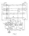
- the data processing system includes a central processing unit (CPU) 10 having an address output port 11 for producing an output address signal.
- the address output port 11 will later be described in detail.
- the output address signal consists of (n + 1) bits arranged from a most significant bit or an n-th bit 2 n to a least significant bit or a zeroth bit 20, where n represents a first predetermined natural number.
- the zeroth through the n-th bits 20 to 2 n of the output address signal are depicted at A0 to A n , respectively.
- the central processing unit 10 further has a CPU input/output port 12 which will later be described in detail.
- the data processing system further comprises a plurality of peripheral units.
- the peripheral units are divided into a specific one and remaining ones which will become clear as the description proceeds.
- the specific one of the peripheral units namely, a specific peripheral unit, is a read-only memory (ROM) 20 which has a memory capacity of 2 n+1 bytes.
- the read-only memory 20 has an ROM address input port 21 for receiving an ROM input address signal.
- the ROM address input port 21 will later be described in detail.
- the ROM input address signal consists of (n + 1) bits arranged from the most significant bit 2 n to the least significant bit 20.
- the ROM address input port 21 is directly supplied with the n bits among the (n + 1) bits of the output address signal as the n bits among the (n + 1) bits of the ROM input address signal.
- the n bits of each of the output and the input address signals are the (n + 1) bits except for an m-th bit 2 m as counted from the least significant bit 20, where m represents a second predetermined natural number which is not greater than the first predetermined natural number.
- the read-only memory 20 has a program memory area (now shown) for memorizing a program which the central processing unit 10 should carry out.
- the read-only memory 20 further has an ROM input/output port 22 and an ROM selection input terminal 23.
- the ROM input/output port 22 is connected to the CPU input/output port 12 through an input/output bus 25. In the manner which will later become clear, the input/output bus 25 is divided into a data bus and a control bus.
- the ROM selection input terminal 23 is for receiving an ROM selection signal which will later become clear.
- the address output port 11 of the central processing unit 10 comprises zeroth through n-th address output terminals 11-0, 11-1, ..., 11-(m-1), 11-m, 11-(m+1), ..., 11-(n-1), and 11-n for producing the zeroth through the n-th bits A0, A1, ..., A m-1 , A m , A m+1 , ..., A n-1 , and A n , respectively.
- the ROM address input port 21 of the read-only memory 20 comprises zeroth through n-th address output terminals 21-0, 21-1, ..., 21-(m-1), 21-m, 21-(m+1), ..., 21-(n-1), and 21-n.
- the zeroth through the (m-1)-th output terminals 21-0 to 21-(m-1) of the ROM address input port 21 are supplied with, as the zeroth through the (m-1)-th bits 20 to 2 m-1 of the ROM input address signal, the zeroth through the (m-1)-th bits A0 to A m-1 from the zeroth through the (m-1)-th address output terminals 11-0 to 11-(m-1) of the address output port 11.
- the (m+1)-th through the n-th output terminals 21-(m+1) to 21-n of the ROM address input port 21 are supplied with, as the (m+1)-th through the n-th bits 2 m+1 to 2 n of the ROM input address signal, the (m+1)-th through the n-th bits A m+1 to A n from the (m+1)-th through the n-th address output terminals 11-(m+1) to 11-n of the address output port 11.
- the m-th output terminal 21-m of the ROM address input port 21 is supplied through a connection line 27 with, as the m-th bit 2 m of the ROM input address signal, a processed bit G which will later become clear.
- the (m+1)-th through the n-th bits A m+1 to A n of the output address signal are supplied to the remaining ones of the peripheral units, namely, remaining peripheral units which are depicted at 30 and 40.
- the remaining peripheral units 30 and 40 have peripheral address input ports 31 and 41 for receiving a combination of the (m+1)-th through the n-th bits A m+1 to A n of the output address signal as a peripheral input address signal.
- the remaining peripheral units 30 and 40 further have peripheral input/output ports 32 and 42 and peripheral selection input terminals 33 and 43.
- the peripheral input/output ports 32 and 42 are connected to the CPU input/output port 12 through the input/output bus 25.
- the peripheral selection input terminals 33 and 43 are for receiving peripheral selection signals which will later become clear.
- peripheral units 30 and 40 may be an input/output device for use as an input/output area or a random access memory (RAM) for use as a work area.
- RAM random access memory
- the output address signal is supplied to an address decoder 50.
- the address decoder 50 decodes the output address signal to produce one of first through third selection signals s1, s2, and s3.
- the first selection signal s1 is delivered to the ROM selection input terminal 23 of the read-only memory 20 as the ROM selection signal.
- the second and the third selection signals s2 and s3 are delivered, as the peripheral selection signals, to the peripheral selection input terminals 33 and 43 of the remaining peripheral units 30 and 40, respectively.
- the output address signal has upper (n - m + 1) bits arranged from the most significant bit 2 n to the m-th bit 2 m .
- the upper (n - m + 1) bits consist with the m-th bit A m to the n-th bit A n .
- the address decoder 50 selects the read-only memory 20 as a selected peripheral unit when the upper (n - m + 1) bits A m to A n are not equal to predetermined bits b m to b n (not shown) arranged from the most significant bit 2 n to the m-th bit 2 m .
- the address decoder 50 selects one of the remaining peripheral units 30 and 40 as the selected peripheral unit.
- the address decoder 50 serves as a peripheral selecting arrangement for selecting one of the peripheral units 20, 30, and 40 as the selected peripheral unit.
- the CPU input/output port 12 of the central processing unit 10 produces an address selection control bit as one of output data.
- the address selection control bit is delivered to the peripheral input/output port 32 of the remaining peripheral unit 30 through the input/output bus 25.
- the remaining peripheral unit 30 includes a bit holding circuit 60 which is supplied with the address selection control bit.
- the bit holding circuit 50 is holding the address selection control bit as a held control bit X.
- the held control bit X is supplied to a gate circuit 70 which is supplied with the upper (n - m + 1) bits A m to A n . Responsive to the held control bit X, the gate circuit 70 processes the m-th bit A m of the output address signal into the processed bit G.
- operation of the gate circuit 70 is conditioned by the predetermined bits b m to b n and a particular bit b x .
- the particular bit b x is equal to the m-th bit 2 m of the predetermined bits, namely, the m-th bit b m .
- the gate circuit 70 produces the m-th bit A m of the output address signal as the processed bit G when the held control bit X is not equal to the particular bit b x .
- the gate circuit 70 produces the m-th bit b m of the predetermined bits as the processed bit G when the held control bit X is equal to the particular bit b x and when the upper (n - m + 1) bits of the output address signal are equal to the predetermined bits except for the m-th bit.
- the gate circuit 70 acts as a bit processing arrangement for processing, in response to the held control bit X, the m-th bit A m of the output address signal into the processed bit G.
- the processed bit G is delivered to the m-th output terminal 21-m of the ROM address input port 21 through the connection line 27 as the m-th bit 2 m of the ROM input address signal. That is, the connection line 27 serves as a bit supplying arrangement for supplying the processed bit G as the m-th bit 2 m of the ROM input address signal to the read-only memory 20.
- the central processing unit 10 is directly capable of accessing an address area of 2 n+1 bytes as a directly-accessible address area.
- the directly-accessible address area is divided into first and second address areas.
- the first address area is an area in which the upper (n - m + 1) bits A m to A n of the output address signal are equal to the predetermined bits b m to b n .
- the second address area is another area in which the upper (n - m + 1) bitg A m to A n of the output address signal are not equal to the predetermined bits b m to b n .
- the First address area is assigned to the remaining peripheral units 30 and 40.
- the second address area is assigned to the read-only memory 20.
- the second address area is narrower than the program memory area.
- the central processing unit 10 can not access all of the program memory area.
- the central processing unit 10 can access all of the program memory area by changing the address selection control bit in the manner which will presently be described.
- the central processing unit 10 accesses one of the remaining peripheral units 30 and 40.
- the central processing unit 10 produces the output address signal in which the upper (n - m + 1) bits A m to A n of the output address signal are equal to the predetermined bits b m to b n .
- the address decoder 50 produces one of the second and the third selection signals s2 and s3 that is determined by the zeroth through the (m - 1)-th bits A0 to A m-1 of the output address signal. In other words, the address decoder 50 selects one of the remaining peripheral units 30 and 40 as the selected peripheral unit.
- the program memory area of the read-only memory 20 is divided into first, second, and third memory areas.
- the first memory area is an area where the m-th through the n-th bits of the ROM input address signal are equal to the predetermined bits b m to b n .
- the second memory area is another area where the m-th through the n-th bits of the ROM input address signal are equal to the predetermined bits b m to b n except for the m-th bit 2 m .
- the third memory area is a remaining area equal to combination of areas which are other than the first and the second memory areas among the program memory area.
- the central processing unit 10 accesses the second and the third memory areas of the program memory area of the read-only memory 20.
- the central processing unit 10 produces the address selection control bit which is not equal to the particular bit b x .
- the bit holding circuit 60 holds the address selection control bit as the held control bit X.
- the central processing unit 10 produces the output address signal in which the upper (n - m + 1) bits A m to A n of the output address signal are not equal to the predetermined bits b m to b n .
- the address decoder 50 selects the read-only memory 20 as the selected peripheral unit.
- the gate circuit 70 produces the m-th bit A m of the output address signal as the processed bit G. Accordingly, the read-only memory 20 is supplied with the output address signal as the input address signal.
- the central processing unit 10 accesses the first and the third memory areas of the program memory area of the read-only memory 20.
- the central processing unit 10 produces the address selection control bit which is equal to the particular bit b x .
- the bit holding circuit 60 holds the address selection control bit as the held control bit X.
- the central processing unit 10 produces the output address signal in which the upper (n - m + 1) bits of the output address signal are not equal to the predetermined bits. Responsive to the output address signal, the address decoder 50 selects the read-only memory 20 as the selected peripheral unit.
- the central processing unit 10 produces the output address signal in which the upper (n - m + 1) bits of the output address signal are equal to the predetermined bits except for the m-th bit.
- the gate circuit 70 produces the m-th bit b m of the predetermined bits as the processed bit G.
- the read-only memory 20 is supplied with the input address signal equal to the output address signal except for the m-th bit 2 m . That is, the output address signal is supplied to the read-only memory 20 as the input address signal with the m-th bit b m of the predetermined bits substituted for the m-th bit A m of the output address signal.
- the central processing unit 10 can access not only the remaining peripheral units 30 and 40 but also the first and the third memory areas of the program memory area of the read-only memory 20.
- the central processing unit 10 is capable of accessing all of the program memory area of the read-only memory 20.
- Fig. 2 shows an example of the gate circuit 70.
- each of the predetermined bits b m to b n has a logic one value.
- the particular bit b x has a logic one value.
- the gate circuit 70 comprises an AND circuit 71 and an OR circuit 72.
- the AND circuit 71 carries out an AND operation on the held control bit X and the (n - m) bits of the upper (n - m + 1) bits except for the m-th bit A m , namely, A m+1 to A n to produce an AND'ed bit.
- the OR circuit 72 carries out an OR operation on the AND'ed bit and the m-th bit A m of the upper (n - m + 1) bits to produce an OR'ed bit as the processed bit G.
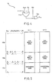
- Fig. 3 shows an address space which the central processing unit 10 can use when the gate circuit 70 shown in Fig. 2 is employed.
- the address space is divided into first, second, and third partial address spaces 81, 82, and 83.
- the first partial address space 81 is a space where each of the upper (n - m + 1) bits A m to A n of the output address signal has a logic one value.
- the zeroth through the (m-1)-th bits A0 to A m-1 are variable.
- the second partial address space 82 is another space where each of the (n - m) bits A m+1 to A n of the upper (n - m + 1) bits has a logic one value and the m-th bit A m of the upper (n - m + 1) bits has a logic zero value.
- the third partial address space 83 is a remaining space equal to combination of spaces which are other than the first and the second partial address spaces 81 and 82 among the address space of the central processing unit 10.
- the third partial address space 83 is mapped into the third memory area of the program memory area of the read-only memory 20 no matter whether the held control bit X has the logic zero value or the logic one value.
- the second partial address space 82 is mapped into the second memory area of the program memory area of the read-only memory 20 when the held control bit X has the logic zero value.
- the second partial address space 82 is mapped into the first memory area of the program memory area of the read-only memory 20 when the held control bit X has the logic one value.
- Fig. 4 shows another example of the gate circuit 70.
- each of the predetermined bits b m to b n has a logic zero value.
- the particular bit b x has a logic zero value.
- the gate circuit 70 comprises an OR circuit 7la and an AND circuit 72a.
- the OR circuit 71a carries out an OR operation on the held control bit X and the (n - m) bits of the upper (n - m + 1) bits except for the m-th bit A m , namely, A m+1 to A n to produce an OR'ed bit.
- the AND circuit 72a carries out an AND operation on the OR'ed bit and the m-th bit A m of the upper (n - m + 1) bits to produce an AND'ed bit as the processed bit G.
- Fig. 5 shows an address space which the central processing unit 10 can use when the gate circuit 70 shown in Fig. 4 is employed.
- the address space is divided into first, second, and third partial address spaces 81a, 82a, and 83a.
- the first partial address space 81a is a space where each of the upper (n - m + 1) bits A m to A n of the output address signal has a logic zero value.
- the second partial address space 82a is another space where each of the (n - m) bits A m+1 to A n of the upper (n - m + 1) bits has a logic zero value and the m-th bit A m of the upper (n - m + 1) bits has a logic one value.
- the third partial address space 83a is a remaining space equal to a space which is other than the first and the second partial address spaces 81a and 82a among the address space of the central processing unit 10.
- the first partial address space 81a is mapped into the peripheral area no matter whether the held control bit X has the logic one value of the logic zero value.
- the third partial address space 83a is mapped into the third memory area of the program memory area of the read-only memory 20 no matter whether the held control bit X has the logic one value of the logic zero value.
- the second partial address space 82a is mapped into the second memory area of the program memory area of the read-only memory 20 when the held control bit X has the logic one value.
- the second partial address space 82a is mapped into the first memory area of the program memory area of the read-only memory 20 when the held control bit X has the logic zero value.
- Fig. 6 shows an example of the data processing system according to this invention that is control equipment for use in an automobile telephone terminal.
- the first predetermined natural number n is equal to fifteen.
- the second predetermined natural number m is equal to thirteen. It is assumed that each of the predetermined bits b13 to b15 has the logic one value and the particular bit b x has the logic one value.
- the remaining peripheral unit 40 is the random access memory (RAM) for use as the work area.
- the input/output bus 25 is divided into the data bus and the control bus which are depicted at 25-1 and 25-2, respectively.
- the central processing unit 10 delivers a read-out instruction signal RD and a write-in instruction signal WR to the control bus 25-2.
- the central processing unit 10 also delivers the address selection control bit depicted at AS to the bit holding circuit 60 through the data bus 25-1.
- the central processing unit 10 receives an interruption signal INT from one of input/output (I/O) devices (not shown) which are the remaining peripheral units.
- a combination of the input/output devices is for use as an input/output area.
- the read-only memory 20 has the memory capacity of 64 Kbytes.
- the random access memory has a memory capacity of 8 Kbytes.
- the bit holding circuit 60 comprises a type D flip-flop 61 and an NOR circuit 62. Responsive to the write-in instruction signal WR supplied from the central processing unit 10 and to the second selection signal s2 supplied from the address decoder 50, the NOR circuit 62 produces a holding instruction signal. Responsive to the holding instruction signal, the type D flip-flop 61 holds the address selection control bit AS as the held control bit X. Supplied with a reset signal RST, the type D flip-flop 61 produces the held control bit X having the logic zero value.
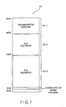
- the program memory area of the read-only memory 20 is divided into the first, the second, and the third memory areas which are depicted at 20-1, 20-2, and 20-3, respectively.
- the first memory area 20-1 is indicated by an address extent which is between hexadecimal E000 and hexadecimal FFFF.
- the first memory area 20-1 memorizes an interruption routine.
- the second memory area 20-2 is indicated by another extent which is between hexadecimal C000 and hexadecimal DFFF.
- the second memory area 20-2 memorizes a first sequence.
- the third memory area 20-3 is indicated by a remaining extent which ranges from hexadecimal 0000 to hexadecimal BFFF.
- the third memory area 20-3 memorizes a second sequence and an interruption start program which is memorized in a memory address of hexadecimal 0038.
- the first partial address space 81 is indicated by an address extent ranging from hexadecimal E000 to hexadecimal FFFF.
- the first partial address space 81 is divided into first and second portions 81-1 and 81-2.
- the first portion 81-1 is indicated by an address extent between hexadecimal F800 and hexadecimal FFFF.
- the second portion is indicated by another address extent between hexadecimal E000 and hexadecimal E7FF.
- the first portion 81-1 of the first partial address space 81 is mapped into the input/output area no matter whether the held control bit X has the logic zero value or the logic one value.
- the second portion 81-2 of the first partial address space 81 is mapped into the work area no matter whether the held control bit X has the logic zero value or the logic one value.
- the third partial address space 83 is indicated by an address extent between hexadecimal 0000 and hexadecimal BFFF.
- the third partial address space 83 is mapped into the third memory area 20-3 for the second sequence and the interruption start program no matter whether the held control bit X has the logic zero value or the logic one value.
- the second partial memory area 20-2 is indicated by an address extent between hexadecimal C000 and hexadecimal DFFF.
- the second partial memory area 20-2 is mapped into the second memory area 20-2 for the first sequence when the held control bit X has the logic zero value.
- the second partial memory area 20-2 is mapped into the first memory area 20-1 for the interruption routine when the held control bit X has the logic one value.
- the bit holding circuit 60 produces the held control bit X having the logic zero value.
- the central processing unit 10 can access only a combination of the second and the third memory areas 20-2 and 20-3 of the program area of the read-only memory 20.
- the central processing unit 10 receives the interruption signal INT from one of the input/output devices at a first stage S1
- the central processing unit 10 produces the output address signal indicative of an address of hexadecimal 0038.
- the read-only memory 20 delivers the interruption start program to the central processing unit 10 through the data bus 25-1.
- the central processing unit 10 sends the address selection control bit AS of logic one value to the bit holding circuit 60.
- the bit holding circuit 60 produces the held control bit X having the logic one value at a second stage S2.
- the central processing unit 10 calls the interruption routine at a third stage S3 and executes the interruption routine at a fourth stage S4.
- the central processing unit 10 controls the bit holding circuit 60 to make the bit holding circuit 60 produce the held control bit X having the logic zero value at a fifth stage S5. Thereafter, the process returns to a point of one of the first and the second sequences at which the interruption occurs at a sixth stage S6.
- the gate circuit 70 illustrated in Fig. 1 may process one of the upper (n- m + 1) bits of the output address signal except for the m-th bit into the processed bit.
- gate circuit 70 may process a plurality of bits of the output address signal into a plurality of processed bits which are supplied to the read-only memory 20.
Landscapes
- Engineering & Computer Science (AREA)
- Theoretical Computer Science (AREA)
- Physics & Mathematics (AREA)
- General Engineering & Computer Science (AREA)
- General Physics & Mathematics (AREA)
- Storage Device Security (AREA)
- Communication Control (AREA)
Abstract
Description
- This invention relates to a data processing system and, in particular, to a data processing system including a peripheral control arrangement for controlling a plurality of peripheral units in response to an output address signal which is supplied from a central processing unit.
- A data processing system comprises a central processing unit (CPU) and a plurality of peripheral units. The peripheral units are divided into a specific one and remaining ones. The specific one of the peripheral units, namely, a specific peripheral unit, may be a read-only memory (ROM) having a program memory area for memorizing a program which is carried out by the central processing unit. The remaining ones of the peripheral units, namely, remaining peripheral units, may comprise a random access memory (RAM) for use as a work area and input/output devices for use as an input/output area.
- The central processing unit is connected to the peripheral units through on address bus, a data bus, and a control bus. The central processing unit has an address output port connected to the address bus. The address output port is for producing an output address signal which consists of (n + 1) bits arranged from a most
significant bit 2n to a leastsignificant bit 2⁰, where n represents a first predetermined natural number. The read-only memory has an address input port connected to the address bus. The address input port is for receiving the output address signal as an input address signal which consists of (n + 1) bits arranged from the mostsignificant bit 2n to the leastsignificant bit 2⁰. - Inasmuch as the central processing unit produces the output address signal which is (n + 1) bits long, the central processing unit is directly capable of accessing on address area of 2n+1 bytes. Such an address area includes the program memory area and is herein called a directly-accessible address area. The directly-accessible address area is determined by the number of the bits of the output address signal.
- Recently, almost all of 8-bit central processing units have the address bus of 16 bits long. Therefore, such an 8-bit central processing unit has the directly-accessible address area of 64 Kbytes.
- The central processing unit must access not only the program memory area but also the work area and the input/output area. In other words, the central processing unit must access, as an accessing address area, a wider address area which is equal to a sum of the program memory area, the work area, and the input/output area. If the central processing unit can access only the directly-accessible address area, the program memory area is limited by an area which is equal to a sum of the work area and the input/output area. Therefore, it is necessary to enlarge the directly-accessible address area to the accessing address area. In order to enlarge an address area accessed by the central processing unit to the accessing address area; various methods are already adopted.
- A first method enlarges the directly-accessible address area to an enlarged address area by using a memory management unit (MMU) for the central processing unit. The memory management unit acts as a peripheral control arrangement for controlling the peripheral units in response to the output address signal so as to enable a selected one of the peripheral units. A second method adopts a central processing unit with the memory management unit. In a third method, the central processing unit is exchanged for a different central processing unit capable of accessing a wider address area which is wider than the directly-accessible address area.
- Each of the first through the third methods can enlarge the directly-accessible address area to the enlarged address area which is several to tens times as wide as the directly-accessible address area.
- The data processing system may be control equipment for use in an automobile telephone terminal. In the control equipment, the program memory area is slightly narrower than the directly-accessible address area but the directly-accessible address area is slightly narrower than the accessing address area which is extremely narrower than the enlarged address area. In this case, each of the first through the third methods is disadvantageous in that an increased number of circuit elements are necessary and that the data processing system becomes expensive.
- It is an object of this invention to provide a data processing system wherein a peripheral control arrangement enables a central processing unit to access an enlarged address area.
- It is another object of this invention to provide a data processing system of the type described, in which the peripheral control arrangement has a simple structure.
- Other objects of this invention will become clear as the description proceeds.
- A data processing system to which this invention is applicable, comprises a central processing unit for producing an output address signal which consists of (n + 1) bits arranged from a most
significant bit 2n to a leastsignificant bit 2⁰, where n represents a first predetermined natural number, a plurality of peripheral units, a specific one of which is for receiving an input address signal consisting of (n + 1) bits arranged from the mostsignificant bit 2n to the leastsignificant bit 2⁰, and a peripheral control arrangement connected to the central processing unit and to the peripheral units for controlling the peripheral units in response to the output address signal so as to enable a selected one of the peripheral units. According to this invention, the specific one of the peripheral units is supplied with the n bits among the (n + 1) bits of the output address signal as the n bits among the (n + 1) bits of the input address signal. The n bits of each of the output and the input address signals are the (n + 1) bits except for an m-th bit 2m as counted from the leastsignificant bit 2⁰, where m represents a second predetermined natural number which is not greater than the first predetermined natural number. The central processing unit produces an address selection control bit. The peripheral control arrangement comprises (1) peripheral selecting means connected to the central processing unit and to the peripheral units for selecting, in response to the output address signal, one of the peripheral units as the selected one of the peripheral units; (2) bit holding means supplied with the address selection control bit for holding the address selection control bit as a held control bit; (3) bit processing means connected to the bit holding means and to the central processing unit for processing, in response to the held control bit, the m-th bit 2m of the output address signal into a processed bit; and (4) bit supplying means connected to the bit processing means and to the specific one of the peripheral units for supplying the processed bit as the m-th bit 2m of the input address signal to the specific one of the peripheral units. -
- Fig. 1 is a block diagram of a data processing system according to an embodiment of the present invention;
- Fig. 2 is a block diagram of a gate circuit for use in the data processing system illustrated in Fig. 1;
- Fig. 3 shows an address space of a central processing unit of the data processing system depicted in Fig. 1 and is for use in describing operation of the data processing system when the gate circuit shown in Fig. 2 is employed;
- Fig. 4 is a block diagram of another gate circuit for use in the data processing system illustrated in Fig. 1;
- Fig. 5 shows another address space of the central processing unit for use in describing operation of the data processing system when the gate circuit shown in Fig. 4 is employed;
- Fig. 6 is a block diagram of control equipment for use in an automobile terminal to which the data processing system according to this invention is applied;
- Fig. 7 shows a program memory area of a read-only memory of the control equipment illustrated in Fig. 6;
- Fig. 8 shows an address space of the central processing unit for use in describing operation of the control equipment illustrated in Fig. 6; and
- Fig. 9 is a flow chart for use in describing operation of the control equipment illustrated in Fig. 6.
- Referring to Fig. 1, the description will begin with a data processing system according to a preferred embodiment of the present invention. The data processing system includes a central processing unit (CPU) 10 having an
address output port 11 for producing an output address signal. Theaddress output port 11 will later be described in detail. The output address signal consists of (n + 1) bits arranged from a most significant bit or an n-th bit 2n to a least significant bit or azeroth bit 2⁰, where n represents a first predetermined natural number. The zeroth through the n-th bits 2⁰ to 2n of the output address signal are depicted at A₀ to An, respectively. Thecentral processing unit 10 further has a CPU input/output port 12 which will later be described in detail. - The data processing system further comprises a plurality of peripheral units. The peripheral units are divided into a specific one and remaining ones which will become clear as the description proceeds. In the example being illustrated, the specific one of the peripheral units, namely, a specific peripheral unit, is a read-only memory (ROM) 20 which has a memory capacity of 2n+1 bytes. The read-
only memory 20 has an ROMaddress input port 21 for receiving an ROM input address signal. The ROMaddress input port 21 will later be described in detail. - The ROM input address signal consists of (n + 1) bits arranged from the most
significant bit 2n to the leastsignificant bit 2⁰. The ROMaddress input port 21 is directly supplied with the n bits among the (n + 1) bits of the output address signal as the n bits among the (n + 1) bits of the ROM input address signal. The n bits of each of the output and the input address signals are the (n + 1) bits except for an m-th bit 2m as counted from the leastsignificant bit 2⁰, where m represents a second predetermined natural number which is not greater than the first predetermined natural number. - The read-
only memory 20 has a program memory area (now shown) for memorizing a program which thecentral processing unit 10 should carry out. The read-only memory 20 further has an ROM input/output port 22 and an ROMselection input terminal 23. The ROM input/output port 22 is connected to the CPU input/output port 12 through an input/output bus 25. In the manner which will later become clear, the input/output bus 25 is divided into a data bus and a control bus. The ROMselection input terminal 23 is for receiving an ROM selection signal which will later become clear. - More specifically, the
address output port 11 of thecentral processing unit 10 comprises zeroth through n-th address output terminals 11-0, 11-1, ..., 11-(m-1), 11-m, 11-(m+1), ..., 11-(n-1), and 11-n for producing the zeroth through the n-th bits A₀, A₁, ..., Am-1, Am, Am+1, ..., An-1, and An, respectively. The ROMaddress input port 21 of the read-only memory 20 comprises zeroth through n-th address output terminals 21-0, 21-1, ..., 21-(m-1), 21-m, 21-(m+1), ..., 21-(n-1), and 21-n. The zeroth through the (m-1)-th output terminals 21-0 to 21-(m-1) of the ROMaddress input port 21 are supplied with, as the zeroth through the (m-1)-th bits 2⁰ to 2m-1 of the ROM input address signal, the zeroth through the (m-1)-th bits A₀ to Am-1 from the zeroth through the (m-1)-th address output terminals 11-0 to 11-(m-1) of theaddress output port 11. The (m+1)-th through the n-th output terminals 21-(m+1) to 21-n of the ROMaddress input port 21 are supplied with, as the (m+1)-th through the n-th bits 2m+1 to 2n of the ROM input address signal, the (m+1)-th through the n-th bits Am+1 to An from the (m+1)-th through the n-th address output terminals 11-(m+1) to 11-n of theaddress output port 11. The m-th output terminal 21-m of the ROMaddress input port 21 is supplied through aconnection line 27 with, as the m-th bit 2m of the ROM input address signal, a processed bit G which will later become clear. - The (m+1)-th through the n-th bits Am+1 to An of the output address signal are supplied to the remaining ones of the peripheral units, namely, remaining peripheral units which are depicted at 30 and 40. The remaining
peripheral units address input ports peripheral units output ports selection input terminals output ports output port 12 through the input/output bus 25. The peripheralselection input terminals - In the manner which will later become clear, the remaining
peripheral units - The output address signal is supplied to an
address decoder 50. Theaddress decoder 50 decodes the output address signal to produce one of first through third selection signals s1, s2, and s3. The first selection signal s1 is delivered to the ROMselection input terminal 23 of the read-only memory 20 as the ROM selection signal. The second and the third selection signals s2 and s3 are delivered, as the peripheral selection signals, to the peripheralselection input terminals peripheral units - More specifically, the output address signal has upper (n - m + 1) bits arranged from the most
significant bit 2n to the m-th bit 2m. Namely, the upper (n - m + 1) bits consist with the m-th bit Am to the n-th bit An. Theaddress decoder 50 selects the read-only memory 20 as a selected peripheral unit when the upper (n - m + 1) bits Am to An are not equal to predetermined bits bm to bn (not shown) arranged from the mostsignificant bit 2n to the m-th bit 2m. When the upper (n - m + 1) bits Am to An are equal to predetermined bits bm to bn, theaddress decoder 50 selects one of the remainingperipheral units address decoder 50 serves as a peripheral selecting arrangement for selecting one of theperipheral units - The CPU input/
output port 12 of thecentral processing unit 10 produces an address selection control bit as one of output data. The address selection control bit is delivered to the peripheral input/output port 32 of the remainingperipheral unit 30 through the input/output bus 25. The remainingperipheral unit 30 includes abit holding circuit 60 which is supplied with the address selection control bit. Thebit holding circuit 50 is holding the address selection control bit as a held control bit X. - The held control bit X is supplied to a
gate circuit 70 which is supplied with the upper (n - m + 1) bits Am to An. Responsive to the held control bit X, thegate circuit 70 processes the m-th bit Am of the output address signal into the processed bit G. - More particularly, operation of the
gate circuit 70 is conditioned by the predetermined bits bm to bn and a particular bit bx. The particular bit bx is equal to the m-th bit 2m of the predetermined bits, namely, the m-th bit bm. Thegate circuit 70 produces the m-th bit Am of the output address signal as the processed bit G when the held control bit X is not equal to the particular bit bx. Thegate circuit 70 produces the m-th bit bm of the predetermined bits as the processed bit G when the held control bit X is equal to the particular bit bx and when the upper (n - m + 1) bits of the output address signal are equal to the predetermined bits except for the m-th bit. At any rate, thegate circuit 70 acts as a bit processing arrangement for processing, in response to the held control bit X, the m-th bit Am of the output address signal into the processed bit G. - As mentioned before, the processed bit G is delivered to the m-th output terminal 21-m of the ROM
address input port 21 through theconnection line 27 as the m-th bit 2m of the ROM input address signal. That is, theconnection line 27 serves as a bit supplying arrangement for supplying the processed bit G as the m-th bit 2m of the ROM input address signal to the read-only memory 20. - With this structure, the
central processing unit 10 is directly capable of accessing an address area of 2n+1 bytes as a directly-accessible address area. The directly-accessible address area is divided into first and second address areas. The first address area is an area in which the upper (n - m + 1) bits Am to An of the output address signal are equal to the predetermined bits bm to bn. The second address area is another area in which the upper (n - m + 1) bitg Am to An of the output address signal are not equal to the predetermined bits bm to bn. The First address area is assigned to the remainingperipheral units only memory 20. Inasmuch as the read-only memory 20 has the program memory area of 2n+1 bytes, the second address area is narrower than the program memory area. In this state, thecentral processing unit 10 can not access all of the program memory area. However, thecentral processing unit 10 can access all of the program memory area by changing the address selection control bit in the manner which will presently be described. - The description will proceed to operation of the data processing system illustrated in Fig. 1.
- At first, the description will be made as regards a first case where the
central processing unit 10 accesses one of the remainingperipheral units central processing unit 10 produces the output address signal in which the upper (n - m + 1) bits Am to An of the output address signal are equal to the predetermined bits bm to bn. When the upper (n - m + 1) bits Am to An are equal to the predetermined bits bm to bn, theaddress decoder 50 produces one of the second and the third selection signals s2 and s3 that is determined by the zeroth through the (m - 1)-th bits A₀ to Am-1 of the output address signal. In other words, theaddress decoder 50 selects one of the remainingperipheral units - The program memory area of the read-
only memory 20 is divided into first, second, and third memory areas. The first memory area is an area where the m-th through the n-th bits of the ROM input address signal are equal to the predetermined bits bm to bn. The second memory area is another area where the m-th through the n-th bits of the ROM input address signal are equal to the predetermined bits bm to bn except for the m-th bit 2m. The third memory area is a remaining area equal to combination of areas which are other than the first and the second memory areas among the program memory area. - The description will be made as regards a second case where the
central processing unit 10 accesses the second and the third memory areas of the program memory area of the read-only memory 20. In this event, thecentral processing unit 10 produces the address selection control bit which is not equal to the particular bit bx. Supplied with the address selection control bit, thebit holding circuit 60 holds the address selection control bit as the held control bit X. After the address selection control bit is produced, thecentral processing unit 10 produces the output address signal in which the upper (n - m + 1) bits Am to An of the output address signal are not equal to the predetermined bits bm to bn. Responsive to the output address signal, theaddress decoder 50 selects the read-only memory 20 as the selected peripheral unit. Responsive to the held control bit X, thegate circuit 70 produces the m-th bit Am of the output address signal as the processed bit G. Accordingly, the read-only memory 20 is supplied with the output address signal as the input address signal. - The description will be made as regards a third case where the
central processing unit 10 accesses the first and the third memory areas of the program memory area of the read-only memory 20. In this event, thecentral processing unit 10 produces the address selection control bit which is equal to the particular bit bx. Supplied with the address selection control bit, thebit holding circuit 60 holds the address selection control bit as the held control bit X. After the address selection control bit is produced, thecentral processing unit 10 produces the output address signal in which the upper (n - m + 1) bits of the output address signal are not equal to the predetermined bits. Responsive to the output address signal, theaddress decoder 50 selects the read-only memory 20 as the selected peripheral unit. - It will be presumed that the
central processing unit 10 produces the output address signal in which the upper (n - m + 1) bits of the output address signal are equal to the predetermined bits except for the m-th bit. In this event, thegate circuit 70 produces the m-th bit bm of the predetermined bits as the processed bit G. Accordingly, the read-only memory 20 is supplied with the input address signal equal to the output address signal except for the m-th bit 2m. That is, the output address signal is supplied to the read-only memory 20 as the input address signal with the m-th bit bm of the predetermined bits substituted for the m-th bit Am of the output address signal. In the third case, thecentral processing unit 10 can access not only the remainingperipheral units only memory 20. - As a result, the
central processing unit 10 is capable of accessing all of the program memory area of the read-only memory 20. - Fig. 2 shows an example of the
gate circuit 70. For the example being illustrated, each of the predetermined bits bm to bn has a logic one value. The particular bit bx has a logic one value. Thegate circuit 70 comprises an ANDcircuit 71 and anOR circuit 72. The ANDcircuit 71 carries out an AND operation on the held control bit X and the (n - m) bits of the upper (n - m + 1) bits except for the m-th bit Am, namely, Am+1 to An to produce an AND'ed bit. The ORcircuit 72 carries out an OR operation on the AND'ed bit and the m-th bit Am of the upper (n - m + 1) bits to produce an OR'ed bit as the processed bit G. - Fig. 3 shows an address space which the
central processing unit 10 can use when thegate circuit 70 shown in Fig. 2 is employed. The address space is divided into first, second, and thirdpartial address spaces partial address space 81 is a space where each of the upper (n - m + 1) bits Am to An of the output address signal has a logic one value. The zeroth through the (m-1)-th bits A₀ to Am-1 are variable. The secondpartial address space 82 is another space where each of the (n - m) bits Am+1 to An of the upper (n - m + 1) bits has a logic one value and the m-th bit Am of the upper (n - m + 1) bits has a logic zero value. The thirdpartial address space 83 is a remaining space equal to combination of spaces which are other than the first and the secondpartial address spaces central processing unit 10. - The first through the third
partial address spaces 81 to 83 are mapped into memory and peripheral areas when the held control bit X has a logic zero or a logic one value, that is, the X = 0 and X = 1. More particularly, the firstpartial address space 81 is mapped into the peripheral area which is used by the remainingperipheral units partial address space 83 is mapped into the third memory area of the program memory area of the read-only memory 20 no matter whether the held control bit X has the logic zero value or the logic one value. The secondpartial address space 82 is mapped into the second memory area of the program memory area of the read-only memory 20 when the held control bit X has the logic zero value. The secondpartial address space 82 is mapped into the first memory area of the program memory area of the read-only memory 20 when the held control bit X has the logic one value. - Fig. 4 shows another example of the
gate circuit 70. For the example being illustrated, each of the predetermined bits bm to bn has a logic zero value. The particular bit bx has a logic zero value. Thegate circuit 70 comprises an OR circuit 7la and an ANDcircuit 72a. The ORcircuit 71a carries out an OR operation on the held control bit X and the (n - m) bits of the upper (n - m + 1) bits except for the m-th bit Am, namely, Am+1 to An to produce an OR'ed bit. The ANDcircuit 72a carries out an AND operation on the OR'ed bit and the m-th bit Am of the upper (n - m + 1) bits to produce an AND'ed bit as the processed bit G. - Fig. 5 shows an address space which the
central processing unit 10 can use when thegate circuit 70 shown in Fig. 4 is employed. The address space is divided into first, second, and thirdpartial address spaces partial address space 81a is a space where each of the upper (n - m + 1) bits Am to An of the output address signal has a logic zero value. The secondpartial address space 82a is another space where each of the (n - m) bits Am+1 to An of the upper (n - m + 1) bits has a logic zero value and the m-th bit Am of the upper (n - m + 1) bits has a logic one value. The thirdpartial address space 83a is a remaining space equal to a space which is other than the first and the secondpartial address spaces central processing unit 10. - The first
partial address space 81a is mapped into the peripheral area no matter whether the held control bit X has the logic one value of the logic zero value. The thirdpartial address space 83a is mapped into the third memory area of the program memory area of the read-only memory 20 no matter whether the held control bit X has the logic one value of the logic zero value. The secondpartial address space 82a is mapped into the second memory area of the program memory area of the read-only memory 20 when the held control bit X has the logic one value. The secondpartial address space 82a is mapped into the first memory area of the program memory area of the read-only memory 20 when the held control bit X has the logic zero value. - Fig. 6 shows an example of the data processing system according to this invention that is control equipment for use in an automobile telephone terminal. For the example being illustrated, the first predetermined natural number n is equal to fifteen. The second predetermined natural number m is equal to thirteen. It is assumed that each of the predetermined bits b₁₃ to b₁₅ has the logic one value and the particular bit bx has the logic one value.
- In the example being illustrated, the remaining
peripheral unit 40 is the random access memory (RAM) for use as the work area. The input/output bus 25 is divided into the data bus and the control bus which are depicted at 25-1 and 25-2, respectively. Thecentral processing unit 10 delivers a read-out instruction signal RD and a write-in instruction signal WR to the control bus 25-2. Thecentral processing unit 10 also delivers the address selection control bit depicted at AS to thebit holding circuit 60 through the data bus 25-1. Thecentral processing unit 10 receives an interruption signal INT from one of input/output (I/O) devices (not shown) which are the remaining peripheral units. A combination of the input/output devices is for use as an input/output area. The read-only memory 20 has the memory capacity of 64 Kbytes. The random access memory has a memory capacity of 8 Kbytes. - The
bit holding circuit 60 comprises a type D flip-flop 61 and an NORcircuit 62. Responsive to the write-in instruction signal WR supplied from thecentral processing unit 10 and to the second selection signal s2 supplied from theaddress decoder 50, the NORcircuit 62 produces a holding instruction signal. Responsive to the holding instruction signal, the type D flip-flop 61 holds the address selection control bit AS as the held control bit X. Supplied with a reset signal RST, the type D flip-flop 61 produces the held control bit X having the logic zero value. - Referring to Fig. 7, the program memory area of the read-
only memory 20 is divided into the first, the second, and the third memory areas which are depicted at 20-1, 20-2, and 20-3, respectively. The first memory area 20-1 is indicated by an address extent which is between hexadecimal E000 and hexadecimal FFFF. The first memory area 20-1 memorizes an interruption routine. The second memory area 20-2 is indicated by another extent which is between hexadecimal C000 and hexadecimal DFFF. The second memory area 20-2 memorizes a first sequence. The third memory area 20-3 is indicated by a remaining extent which ranges from hexadecimal 0000 to hexadecimal BFFF. The third memory area 20-3 memorizes a second sequence and an interruption start program which is memorized in a memory address of hexadecimal 0038. - Referring to Fig. 8, the first
partial address space 81 is indicated by an address extent ranging from hexadecimal E000 to hexadecimal FFFF. The firstpartial address space 81 is divided into first and second portions 81-1 and 81-2. The first portion 81-1 is indicated by an address extent between hexadecimal F800 and hexadecimal FFFF. The second portion is indicated by another address extent between hexadecimal E000 and hexadecimal E7FF. The first portion 81-1 of the firstpartial address space 81 is mapped into the input/output area no matter whether the held control bit X has the logic zero value or the logic one value. The second portion 81-2 of the firstpartial address space 81 is mapped into the work area no matter whether the held control bit X has the logic zero value or the logic one value. - The third
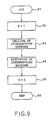
partial address space 83 is indicated by an address extent between hexadecimal 0000 and hexadecimal BFFF. The thirdpartial address space 83 is mapped into the third memory area 20-3 for the second sequence and the interruption start program no matter whether the held control bit X has the logic zero value or the logic one value. The second partial memory area 20-2 is indicated by an address extent between hexadecimal C000 and hexadecimal DFFF. The second partial memory area 20-2 is mapped into the second memory area 20-2 for the first sequence when the held control bit X has the logic zero value. The second partial memory area 20-2 is mapped into the first memory area 20-1 for the interruption routine when the held control bit X has the logic one value. - Referring to Fig. 9, the description will proceed to operation of the control equipment of the automobile telephone terminal shown in Fig. 6. In the automobile telephone terminal, a real time processing is activated by interruption.
- Supplied with the reset signal RST, the
bit holding circuit 60 produces the held control bit X having the logic zero value. In this event, thecentral processing unit 10 can access only a combination of the second and the third memory areas 20-2 and 20-3 of the program area of the read-only memory 20. When thecentral processing unit 10 receives the interruption signal INT from one of the input/output devices at a first stage S1, thecentral processing unit 10 produces the output address signal indicative of an address of hexadecimal 0038. Responsive to the output address signal, the read-only memory 20 delivers the interruption start program to thecentral processing unit 10 through the data bus 25-1. Responsive to the interruption start program, thecentral processing unit 10 sends the address selection control bit AS of logic one value to thebit holding circuit 60. Responsive to the address selection control bit AS, thebit holding circuit 60 produces the held control bit X having the logic one value at a second stage S2. - The
central processing unit 10 calls the interruption routine at a third stage S3 and executes the interruption routine at a fourth stage S4. When execution of the interruption routine comes to an end, thecentral processing unit 10 controls thebit holding circuit 60 to make thebit holding circuit 60 produce the held control bit X having the logic zero value at a fifth stage S5. Thereafter, the process returns to a point of one of the first and the second sequences at which the interruption occurs at a sixth stage S6. - While this invention has thus far been described in conjunction with a preferred embodiment thereof, it will readily be possible for those skilled in the art to put this invention into practice in various other manners. For example, the
gate circuit 70 illustrated in Fig. 1 may process one of the upper (n- m + 1) bits of the output address signal except for the m-th bit into the processed bit. In addition,gate circuit 70 may process a plurality of bits of the output address signal into a plurality of processed bits which are supplied to the read-only memory 20.
Claims (7)
said specific one of the peripheral units is supplied with the n bits among said (n + 1) bits of the output address signal as the n bits among said (n + 1) bits of the input address signal, said n bits of each of said output and said input address signals being the (n + 1) bits except for an m-th bit 2m as counted from said least significant bit 2⁰, where m represents a second predetermined natural number which is not greater than said first predetermined natural number;
said central processing unit producing an address selection control bit;
said peripheral control arrangement comprising:
peripheral selecting means connected to said central processing unit and to said peripheral units for selecting, in response to said output address signal, one of the peripheral units as said selected one of the peripheral units;
bit holding means supplied with said address selection control bit for holding said address selection control bit as a held control bit;
bit processing means connected to said bit holding means and to said central processing unit for processing, in response to said held control bit, said m-th bit 2m of the output address signal into a processed bit; and
bit supplying means connected to said bit processing means and to said specific one of the peripheral units for supplying said processed bit as said m-th bit 2m of the input address signal to said specific one of the peripheral units.
Applications Claiming Priority (2)
| Application Number | Priority Date | Filing Date | Title |
|---|---|---|---|
| JP269947/88 | 1988-10-26 | ||
| JP26994788A JPH077353B2 (en) | 1988-10-26 | 1988-10-26 | Address selection method |
Publications (3)
| Publication Number | Publication Date |
|---|---|
| EP0366458A2 true EP0366458A2 (en) | 1990-05-02 |
| EP0366458A3 EP0366458A3 (en) | 1991-04-17 |
| EP0366458B1 EP0366458B1 (en) | 1995-06-28 |
Family
ID=17479424
Family Applications (1)
| Application Number | Title | Priority Date | Filing Date |
|---|---|---|---|
| EP19890311039 Expired - Lifetime EP0366458B1 (en) | 1988-10-26 | 1989-10-26 | Data processing system wherein a simple peripheral control arrangement enables a CPU to access an enlarged address area |
Country Status (3)
| Country | Link |
|---|---|
| EP (1) | EP0366458B1 (en) |
| JP (1) | JPH077353B2 (en) |
| AU (1) | AU615587B2 (en) |
Cited By (1)
| Publication number | Priority date | Publication date | Assignee | Title |
|---|---|---|---|---|
| EP0393281A2 (en) * | 1989-04-20 | 1990-10-24 | International Control Automation Finance S.A. | Method and apparatus for shadowing memory |
Families Citing this family (1)
| Publication number | Priority date | Publication date | Assignee | Title |
|---|---|---|---|---|
| JP4771609B2 (en) * | 2000-05-08 | 2011-09-14 | フルタ電機株式会社 | Planter with air purifier |
Citations (1)
| Publication number | Priority date | Publication date | Assignee | Title |
|---|---|---|---|---|
| JPS54142025A (en) * | 1978-04-27 | 1979-11-05 | Toshiba Corp | Address system |
-
1988
- 1988-10-26 JP JP26994788A patent/JPH077353B2/en not_active Expired - Lifetime
-
1989
- 1989-10-26 AU AU43808/89A patent/AU615587B2/en not_active Ceased
- 1989-10-26 EP EP19890311039 patent/EP0366458B1/en not_active Expired - Lifetime
Patent Citations (1)
| Publication number | Priority date | Publication date | Assignee | Title |
|---|---|---|---|---|
| JPS54142025A (en) * | 1978-04-27 | 1979-11-05 | Toshiba Corp | Address system |
Non-Patent Citations (4)
| Title |
|---|
| E.D.N. ELECTRICAL DESIGN NEWS, vol. 30, no. 20, September 1985, pages 303-304, Newton Massachusetts, US; J. HARDWAY: "146805 muP addresses an extra 10K bytes" * |
| EDN - ELECTRICAL DESIGN NEWS, vol. 32, no. 9, 30th April 1987, pages 189-194,196,198, Newton, MA, US; T. KENDALL: "Page addressing expands addressable memory in muP systems" * |
| ELECTRONIC DESIGN, vol. 26, no. 9, April 1978, pages 84-92; G. FIELLAND et al.: "Keep the memory interface simple" * |
| PATENT ABSTRACTS OF JAPAN, vol. 4, no. 1 (E-163), 8th January 1980, page 107 E 163; & JP-A-54 142 025 (TOKYO SHIBAURA DENKI K.K.) 05-11-1979 * |
Cited By (3)
| Publication number | Priority date | Publication date | Assignee | Title |
|---|---|---|---|---|
| EP0393281A2 (en) * | 1989-04-20 | 1990-10-24 | International Control Automation Finance S.A. | Method and apparatus for shadowing memory |
| EP0393281A3 (en) * | 1989-04-20 | 1991-07-10 | International Control Automation Finance S.A. | Method and apparatus for shadowing memory |
| US5410665A (en) * | 1989-04-20 | 1995-04-25 | Elsag International B.V. | Process controller single memory chip shadowing technique |
Also Published As
| Publication number | Publication date |
|---|---|
| EP0366458A3 (en) | 1991-04-17 |
| AU4380889A (en) | 1990-05-03 |
| JPH02116939A (en) | 1990-05-01 |
| EP0366458B1 (en) | 1995-06-28 |
| JPH077353B2 (en) | 1995-01-30 |
| AU615587B2 (en) | 1991-10-03 |
Similar Documents
| Publication | Publication Date | Title |
|---|---|---|
| US4373181A (en) | Dynamic device address assignment mechanism for a data processing system | |
| US4591973A (en) | Input/output system and method for digital computers | |
| US5109334A (en) | Memory management unit capable of expanding the offset part of the physical address | |
| US4755934A (en) | System for selecting an address in an input/output board | |
| EP0085048A4 (en) | Extended addressing apparatus and method for direct storage access devices. | |
| EP0338317B1 (en) | Information processor operative both in direct mapping and in bank mapping and the method of switching the mapping schemes | |
| EP0366458A2 (en) | Data processing system wherein a simple peripheral control arrangement enables a CPU to access an enlarged address area | |
| EP0057096B1 (en) | Information processing unit | |
| CA1304517C (en) | Multiple computer interface | |
| EP0118669B1 (en) | Channel subsystem | |
| EP0513829B1 (en) | Fuzzy reasoning processor and method, and rule setting apparatus and method | |
| EP0261947A1 (en) | Computer system | |
| US4388707A (en) | Memory selecting system | |
| EP0173746A1 (en) | System of selecting address in input/output board | |
| US6311266B1 (en) | Instruction look-ahead system and hardware | |
| US5388239A (en) | Operand address modification system | |
| US4737906A (en) | Multiple virtual control unit | |
| JPH0148570B2 (en) | ||
| EP0172342A2 (en) | Bus control gate array | |
| JP2918570B2 (en) | Central processing unit | |
| JP2666419B2 (en) | Information processing device | |
| JP2680013B2 (en) | External I / O control circuit of programmable controller | |
| EP0424889A2 (en) | A memory management system for reallocating memory space based on data set in registers | |
| KR850000978Y1 (en) | Interface circuit for memory board | |
| JPS62154050A (en) | Data processing system for control equipment |
Legal Events
| Date | Code | Title | Description |
|---|---|---|---|
| PUAI | Public reference made under article 153(3) epc to a published international application that has entered the european phase |
Free format text: ORIGINAL CODE: 0009012 |
|
| 17P | Request for examination filed |
Effective date: 19891124 |
|
| AK | Designated contracting states |
Kind code of ref document: A2 Designated state(s): FR GB SE |
|
| PUAL | Search report despatched |
Free format text: ORIGINAL CODE: 0009013 |
|
| AK | Designated contracting states |
Kind code of ref document: A3 Designated state(s): FR GB SE |
|
| 17Q | First examination report despatched |
Effective date: 19931214 |
|
| GRAA | (expected) grant |
Free format text: ORIGINAL CODE: 0009210 |
|
| AK | Designated contracting states |
Kind code of ref document: B1 Designated state(s): FR GB SE |
|
| ET | Fr: translation filed | ||
| PLBE | No opposition filed within time limit |
Free format text: ORIGINAL CODE: 0009261 |
|
| STAA | Information on the status of an ep patent application or granted ep patent |
Free format text: STATUS: NO OPPOSITION FILED WITHIN TIME LIMIT |
|
| 26N | No opposition filed | ||
| PGFP | Annual fee paid to national office [announced via postgrant information from national office to epo] |
Ref country code: SE Payment date: 19971009 Year of fee payment: 9 |
|
| PG25 | Lapsed in a contracting state [announced via postgrant information from national office to epo] |
Ref country code: SE Free format text: LAPSE BECAUSE OF NON-PAYMENT OF DUE FEES Effective date: 19981027 |
|
| EUG | Se: european patent has lapsed |
Ref document number: 89311039.5 |
|
| PGFP | Annual fee paid to national office [announced via postgrant information from national office to epo] |
Ref country code: FR Payment date: 20011010 Year of fee payment: 13 |
|
| PGFP | Annual fee paid to national office [announced via postgrant information from national office to epo] |
Ref country code: GB Payment date: 20011024 Year of fee payment: 13 |
|
| REG | Reference to a national code |
Ref country code: GB Ref legal event code: IF02 |
|
| PG25 | Lapsed in a contracting state [announced via postgrant information from national office to epo] |
Ref country code: GB Free format text: LAPSE BECAUSE OF NON-PAYMENT OF DUE FEES Effective date: 20021026 |
|
| GBPC | Gb: european patent ceased through non-payment of renewal fee | ||
| PG25 | Lapsed in a contracting state [announced via postgrant information from national office to epo] |
Ref country code: FR Free format text: LAPSE BECAUSE OF NON-PAYMENT OF DUE FEES Effective date: 20030630 |
|
| REG | Reference to a national code |
Ref country code: FR Ref legal event code: ST |