EP0366587A2 - Semiconductor devices having closely spaced device regions formed using a self aligning reverse image fabrication process - Google Patents
Semiconductor devices having closely spaced device regions formed using a self aligning reverse image fabrication process Download PDFInfo
- Publication number
- EP0366587A2 EP0366587A2 EP89480155A EP89480155A EP0366587A2 EP 0366587 A2 EP0366587 A2 EP 0366587A2 EP 89480155 A EP89480155 A EP 89480155A EP 89480155 A EP89480155 A EP 89480155A EP 0366587 A2 EP0366587 A2 EP 0366587A2
- Authority
- EP
- European Patent Office
- Prior art keywords
- forming
- layer
- stud
- sidewall
- regions
- Prior art date
- Legal status (The legal status is an assumption and is not a legal conclusion. Google has not performed a legal analysis and makes no representation as to the accuracy of the status listed.)
- Granted
Links
Images


Classifications
-
- H—ELECTRICITY
- H01—ELECTRIC ELEMENTS
- H01L—SEMICONDUCTOR DEVICES NOT COVERED BY CLASS H10
- H01L21/00—Processes or apparatus adapted for the manufacture or treatment of semiconductor or solid state devices or of parts thereof
- H01L21/70—Manufacture or treatment of devices consisting of a plurality of solid state components formed in or on a common substrate or of parts thereof; Manufacture of integrated circuit devices or of parts thereof
- H01L21/71—Manufacture of specific parts of devices defined in group H01L21/70
- H01L21/768—Applying interconnections to be used for carrying current between separate components within a device comprising conductors and dielectrics
- H01L21/76897—Formation of self-aligned vias or contact plugs, i.e. involving a lithographically uncritical step
-
- H—ELECTRICITY
- H01—ELECTRIC ELEMENTS
- H01L—SEMICONDUCTOR DEVICES NOT COVERED BY CLASS H10
- H01L21/00—Processes or apparatus adapted for the manufacture or treatment of semiconductor or solid state devices or of parts thereof
- H01L21/70—Manufacture or treatment of devices consisting of a plurality of solid state components formed in or on a common substrate or of parts thereof; Manufacture of integrated circuit devices or of parts thereof
- H01L21/77—Manufacture or treatment of devices consisting of a plurality of solid state components or integrated circuits formed in, or on, a common substrate
- H01L21/78—Manufacture or treatment of devices consisting of a plurality of solid state components or integrated circuits formed in, or on, a common substrate with subsequent division of the substrate into plural individual devices
- H01L21/82—Manufacture or treatment of devices consisting of a plurality of solid state components or integrated circuits formed in, or on, a common substrate with subsequent division of the substrate into plural individual devices to produce devices, e.g. integrated circuits, each consisting of a plurality of components
- H01L21/822—Manufacture or treatment of devices consisting of a plurality of solid state components or integrated circuits formed in, or on, a common substrate with subsequent division of the substrate into plural individual devices to produce devices, e.g. integrated circuits, each consisting of a plurality of components the substrate being a semiconductor, using silicon technology
- H01L21/8248—Combination of bipolar and field-effect technology
- H01L21/8249—Bipolar and MOS technology
-
- Y—GENERAL TAGGING OF NEW TECHNOLOGICAL DEVELOPMENTS; GENERAL TAGGING OF CROSS-SECTIONAL TECHNOLOGIES SPANNING OVER SEVERAL SECTIONS OF THE IPC; TECHNICAL SUBJECTS COVERED BY FORMER USPC CROSS-REFERENCE ART COLLECTIONS [XRACs] AND DIGESTS
- Y10—TECHNICAL SUBJECTS COVERED BY FORMER USPC
- Y10S—TECHNICAL SUBJECTS COVERED BY FORMER USPC CROSS-REFERENCE ART COLLECTIONS [XRACs] AND DIGESTS
- Y10S148/00—Metal treatment
- Y10S148/009—Bi-MOS
Definitions
- the present invention relates generally to semiconductor devices and methods of fabricating the same, and more particularly to a self-aligned method for fabricating semiconductor devices using a reverse image process.
- One method of manufacturing semiconductor devices to provide smaller device size and decreased device spacing is that known as "lost wax” or "reverse image” processing.
- a protective structure such as a stud or ridge is formed on a silicon wafer. Doping and/or various other process are performed using the protective structure as a mask. The structure is subsequently removed in the final steps of the process. Examples of such a method include: U.S. Pat. No. 4,571,817 to Birritella et al.; European Patent Application EP 0 128 751 by Toshiba; and J. Jiyamoto et al. "A 1.0 Micron N-Well CMOS/Bipolar Technology for VLSI Circuits", IEDM 1983, pgs 63-66.
- U.S. Pat. No. 4,419,809 to Riseman et al. uses the above-described "lost wax" method to form the drain region of a MOSFET.
- Riseman et al. further shows the use of sidewall technology to form a sub-micron device channel.
- the principal object of the present invention is to provide a new and improved method of fabricating semiconductor devices.
- Another object of the present invention is to provide such a method capable of fabricating small, densely packed semiconductor devices.
- a further object of the present invention is to provide such a method which is economically and efficiently applicable to the fabrication of bipolar, insulated gate, and BICMOS logic devices.
- Yet another object of the present invention is to provide new and improved semiconductor devices having small, densely packed device regions.
- a new and improved method of forming a semiconductor device on a body of semiconductor material having a first doped region of a first conductivity type comprising the steps of: forming a stud over the first doped region; using the stud as a mask to form a second doped region of a second conductivity type in the surface of the first doped region adjoining the stud; forming a sidewall of insulating material on the stud; forming a first device contact within the sidewall; and forming a second device contact over the second doped region adjoining the sidewall, such that the first and second contacts are separated by the sidewall.
- the step of forming the second device contact includes the steps of forming a layer of conductive material generally conformally over the first doped region, the stud, and the sidewall, and then planarizing the layer of conductive material to a height equal to or less than that of the sidewall.
- the second contact is thus self-aligned with the first and second doped regions and the first device contact.
- the method of the present invention can beneficially be utilized to fabricate new and improved bipolar transistors, insulated gate transistors, and BICMOS logic including both types of transistors. It can further be used to fabricate any other type of semiconductor device which utilizes the self-aligned, closely spaced device regions and contacts of the present invention.
- CMOS devices including a pair of N- and P- channel enhancement mode CMOS devices and an NPN bipolar transistor.
- the particular conductivity types and concentrations described herein are exemplary in nature. Through the reversal of conductivity types and/or the appropriate adjustment of conductivity concentrations, it will be apparent to those skilled in the art that the present invention can be used to fabricate CMOS devices of differing concentrations and/or a PNP-type bipolar transistor. It will also be understood that the present invention is not limited to the fabrication of BICMOS devices, but has utility in the fabrication of separate bipolar and insulated gate devices, as well as in the fabrication of other types of semiconductor devices requiring closely spaced, highly aligned device regions.
- a wafer or substrate 10 of P-silicon monocrystalline material is provided, preferably having a ⁇ 100> crystallographic orientation and a resistivity in the range of 10-20 ohms-centimeter.
- An N+ subcollector region 12 is formed in substrate 10, for example by a conventional process of implanting arsenic (As) ions to a concentration in the range of about 1x10¹⁹-1x10²⁰ atoms/cm3.
- As arsenic
- N+ subcollector region 12 can be formed by conventional diffusion processes.
- a P- epitaxial layer 14 is grown on layer 12, for example using a conventional low temperature, low pressure silicon epitaxial process.
- Layer 14 is preferably formed to a thickness in the range of about 0.6-1.5 microns.
- a pair of N well regions 14A, 14C are formed in layer 14 so as to bound an undisturbed P- well region 14B.
- Regions 14A and 14C are formed, for example, by the selective implantation of arsenic or phosphorous (P) ions into layer 14 using standard photolithographic masking processes to block out region 14B.
- Regions 14A, 14C can be completed using conventional dopant drive-in processes.
- each deep isolation region 16, 18, 20, 22 is generally T-shaped, including a deep trench (T-base) extending vertically downward through layer 12, and a shallow T-cap at the surface of the device extending partway into the adjoining wells.
- Adjacent deep isolation regions 16, 18 are used to electrically isolate a transistor device subsequently formed in well 14A.
- adjacent deep isolation regions 18, 20 and 20, 22 are used to electrically isolate transistor devices subsequently formed in wells 14B and 14C, respectively.
- a shallow isolation region 24 is formed at the surface of well 14C, spaced laterally from the T-cap of isolation region 20 to electrically isolate subsequently formed elements of a bipolar transistor. Isolation region 24 is spaced, for example, a distance D1 in the range of about 1-10 microns from the cap of deep isolation region 20, and extends down into well 14C.
- Shallow isolation region 24, as well as the T-caps of deep isolation regions 16, 18, 20, 22, can be formed, for example, using conventional recessed oxide isolation (ROI) or shallow trench isolation processes. Subsequent to the formation of the T-caps of deep isolation regions 16, 18, 20, 22, the deep trenches are formed, for example, by conventional SiO2 or polysilicon filled deep trench isolation methods. The above-described methods of forming shallow and deep isolation regions are well known to those skilled in the art, and may be reversed as desired to form the deep trench regions first.
- an N+ subcollector reachthrough region 28 is formed between isolation regions 20, 24 extending downward from the upper surface of well 14C into subcollector layer 12.
- Region 28 is formed, for example, by a conventional process of diffusing POCl3 into well 14C between isolation regions 20, 24. This diffusion process is followed by a conventional oxidation process such as thermal oxidation in a wet oxygen ambient. This diffusion process drives the phosphorous dopant downward to complete subcollector reachthrough region 28, and forms an oxide layer 34 on the surface of the device.
- Oxide layer 34 is formed, for example, to a thickness of about 100-500 Angstroms, the layer being appreciably thicker at the surface of subcollector reachthrough region 28.
- the surface conductivities of wells 14A, 14B are adjusted where MOS transistors are to be formed, so as to provide desired threshold voltages V T for these transistors.
- MOS transistors MOS transistors
- boron ions are selectively implanted shallowly into the surface of the well to a dosage in the range of about 1-5x10¹²/cm2.
- a layer 36 of conductive material is formed over layer 34.
- suitable conductive materials for layer 36 include high-temperature, high-conductivity conductor such as conductive polysilicon, polycide (comprising polysilicon with a metal silicide coating), and refractory metals such as tungsten silicide (WSi2).
- layer 36 comprises an intrinsic (non-doped) polycrystalline silicon (polysilicon) formed by a conventional chemical vapor deposition (CVD) process to a thickness in then range of about 2,000-6,000 Angstroms.
- CVD chemical vapor deposition
- regions 37A, 37C of the layer, overlying wells 14A, 14C, respectively, are doped to N+ concentrations using conventional, selective As or P ion implantation.
- a region 37B of layer 36, overlying well 14B, is doped to P+ using conventional, selective boron ion implantation.
- polysilicon layer 36 can be formed in situ doped to an N+ concentration in the range of not less than 2x10²⁰ atoms/cm3.
- an optional layer 38 of silicon dioxide can be formed thereon by a conventional CVD process.
- layer 38 is preferably formed to a thickness of about 100-500 Angstroms, and functions to facilitate the delineation of the studs described below, and to relieve interlayer stresses between layer 36 and a subsequently formed nitride layer 40.
- Nitride layer 40 is formed, for example, by a conventional CVD process to a thickness in the range of about 1,000-2,000 Angstroms.
- resist mask regions 42, 44, 46 are centered over regions in wells 14A 14B, respectively, which will subsequently form the gates of completed CMOS transistors.
- Mask region 46 is centered over the surface of well 14C (i.e. the surface between the edges of isolation regions 22, 24), a region which will subsequently form the emitter of a completed bipolar transistor.
- RIE etchants include: CF4+O2 to remove silicon nitride layer 40; CF4+H2 to remove silicon dioxide layer 38; and Cl2+Ar or CF4+O2 to remove polysilicon layer 36.
- the resist mask regions 42, 44, 46 are then stripped with an oxide plasma to delineate studs 48, 50, 52 over wells 14A, 14B, 14C, respectively.
- the portions of the layer remaining in studs 48, 50, 52 are doped to N+, P+, N+, respectively. If layer 36 had been formed in situ doped N+ in accordance with the alternate embodiment described above, these same portions would be doped to N+.
- oxide layer 34 outside the regions of studs 48, 50, 52 is removed, for example through the use of a carbon tetraflouride (CF4) plasma etch or a diluted, buffered hydroflouric acid etch. Because layer 38 was thicker at the surface of subcollector reachthrough 28 than over the remainder of the device surface, a protective portion 60 of the oxide remains after the above-described etch. Subsequent to the removal of layer 34, a photolithographic blocking mask 61 is formed over the surface of the device between isolation regions 18 and 24 so as to mask the surface of well 14B.
- CF4 carbon tetraflouride
- a conventional, blanket boron ion implantation is then performed with a dose in the range of 1x10¹² atoms/cm3 to 1x10¹³ atoms/cm3.
- This boron ion implantation converts the surface region of well 14A not underneath stud 48 into P type lightly doped drain (LDD) regions 54A, 54B, and the surface region of well 14C not underneath stud 52 into P type intrinsic/extrinsic base link-up region 58.
- LDD lightly doped drain
- a pair of photolithographic blocking masks 63, 65 are formed over wells 14A, 14C, respectively.
- a conventional, blanket arsenic ion implantation is performed with a dose in the range of 1-10x1013 atoms/cm2. This implantation converts the surface region of well 14B not underneath stud 50 into N type LDD regions 56A, 56B.
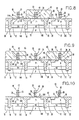
- the resulting device with the photolithographic masks removed is shown in Fig. 10.
- silicon dioxide sidewalls 62 are formed on the sides of each of studs 48, 50, 52.
- the sidewall 62 formed on stud 48 is designated with the suffix A
- the sidewall formed on stud 50 is designated with the suffix C
- the sidewall formed about stud 52 is indicated with the suffix E. From a consideration of the top view in Fig. 11A, it will be appreciated that studs 48, 50 completely bisect what will be the active regions of the subsequently formed CMOS transistors.
- LDD regions 54A, 54B, 56A, 56B comprise electrically separate regions spaced by the studs 48, 50, respectively. Stud 52, however, is situated with its sidewall 62B entirely within what will be the active region of the subsequently formed bipolar transistor.
- Link-up region 58 thus comprises a unitary electrical region surrounding stud 58.
- Sidewalls 62 are formed, for example, by first using a conventional CVD process to form a conformal layer of SiO2 (not shown) to a thickness in the range of about 1,000-5,000 Angstroms. Subsequent to the formation of this conformal layer of SiO2, an anisotropic RIE etchant such as CF4 + O2 is used to remove the horizontal portions of the layer, leaving vertical sidewalls 62.
- a conventional CVD process to form a conformal layer of SiO2 (not shown) to a thickness in the range of about 1,000-5,000 Angstroms.
- an anisotropic RIE etchant such as CF4 + O2 is used to remove the horizontal portions of the layer, leaving vertical sidewalls 62.
- a layer 64 of polycide with accompanying metal silicide surface 64A is deposited conformally over the top of the device to a thickness D2 of at least the vertical height of sidewalls 62, or since the sidewalls cover the vertical surfaces of studs 48, 50, 52, the height of the studs.
- Layer 64 is formed, for example, by a conventional low pressure CVD process.
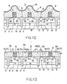
- the layer is planarized evenly with the tops of sidwalls 62 and studs 48, 50, 52 to form the device shown in Fig. 13.
- This planarization is accomplished, for example, by the use of a photoresist reflow and RIE etch-back process or by a chemical-mechanical (chem-mech) polish.
- An acceptable chemical-mechanical polish process is shown in U.S. Patent No. 3,911,562 to Youmans, incorporated herein by reference.
- regions 64B of layer 64 surrounding stud 50 are selectively doped with arsenic (As), while regions 64C of layer 64 surrounding studs 48 and 52 are selectively doped with boron. Both regions 64B and 64C are doped to a concentration in the range of about 1-10x1020 atoms/cm3. Both of these dopings are performed using conventional ion implantation processes with conventional photolithographic masking.
- layer 64 is delineated to form five discrete regions which, for purposes of explanation, are indicated by reference numbers 66A, 66B, 68A, 68B, and 70, region 70 forming a rectangular ring about stud 52 and sidewall 62E.
- Regions 66A, 66B adjoin opposite sidewalls of stud 48, the former overlying LDD implant region 54A and the latter extending from the edge of isolation trench 18 to overlie LDD implant region 54B.
- Regions 68A, 68B adjoin opposite sidewalls of stud 50, with the former extending from an edge of isolation trench 18 to overlie LDD implant region 56A, and the latter extending from an edge of isolation region 20 to overlie LDD implant region 56B.
- Region 70 forms a ring about the sidewalls of stud 52, with the left half (as viewed in the Figs.) extending from an edge of isolation trench 24 to overlie intrinsic-extrinsic base link-up region 58, and the right half extending from an edge of isolation trench 22 to overlie the other side of the link-up region.
- delineation of layer 64 to form regions 66, 68, and 70 as shown in Fig. 14 is accomplished, for example, by the use of an appropriate RIE etchant such as CF4 + H2 in combination with conventional photolithographic masking.
- the device is subjected to thermal oxidation so as to form a layer 72 of SiO2 over the exposed surfaces of these regions to a thickness in the range of about 1,000-5,000 Angstroms.
- Layer 72 is not formed, of course, over the exposed surfaces of the device or over the tops of studs 48, 50, 52 which are protected by the nitride. This last-described process of thermal oxidation further operates on the device of Fig.
- stud 52 over well 14C is removed to leave sidewall 62E bounding an exposed area on the well surface.
- Stud 52 is removed by first etching nitride layer 40 with a CF4/O2 plasma etch or a hot bath of phosphoric acid (H3PO4).
- the relatively thin layer 38 of silicon dioxide is removed by dipping in BHF without substantially disturbing the much thicker layer 72 and sidewall 62E of silicon dioxide.
- Polysilicon layer 36 is removed, for example, with a pyrocathecal etch, and silicon dioxide layer 34 is removed with BHF. It will be appreciated that the step of removing silicon dioxide layer 34 with a BHF dip etch can be carefully controlled to stop at the surface of well 14C so as not to etch into the device surface or otherwise disturb the nature of the subsequently formed bipolar transistor.
- a buried subcollector implant region 74 is formed in well 14C by a conventional implantation of arsenic or phosphorus ions. Because the remainder of the device is masked by polysilicon regions 66A, 66B, 68A, 68C, 70, overlying layer 72, and studs 48, 50, this implantation is effective only in the window opened within sidewall 62E by the removal of stud 52. The surface of subcollector reachthrough 28 is exposed to the implantation. However, the dopant concentration of subcollector reachthrough region 28 is sufficiently larger than that of subcollector region 74 so it is not appreciably altered.
- a conventional, blanket implantation of Boron ions if performed with a dose in the range of 1-10x1012 atoms/cm2 to form an intrinsic base region 75.
- emitter region 76 can be out-diffused from the emitter polysilicon deposited as described hereinbelow, or from a combination of both of these processes. It will be understood that buried region 74, intrinsic base region 75, and emitter region 76 can be formed in interchangeable order.
- the polysilicon regions 66A, 66B, 68A, 68C, 70 overlying layer 72, and studs 48, 50 function as implant blocking masks, in the manner described above, to block the Boron and Arsenic ions from entering the underlying device regions. Also in the manner described above, the dopant concentration of subcollector reachthrough region 28 is sufficiently high that it is left effectively undisturbed.
- a layer 80 of in situ arsenic doped polysilicon having a concentration in the range of about 1-10x1020 atoms/cm3, is formed over the exposed inner surface of sidewall 62E and overlying emitter region 76.
- a layer 82 of metal silicide is formed thereover in the manner shown in Fig. 18 to increase the conductivity of layer 80.
- layer 80 can comprise an intrinsic polysilicon later doped by a conventional implantation with arsenic ions to a concentration in the range of about 1-10x1020 atoms/cm3.
- Layer 80 is formed, for example, by a low pressure CVD process.
- Layer 82 is formed, for example, by physically evaporating or sputtering a thin layer of metal, for example titanium, over layer 80, and converting it into a metal silicide using an alloy sintering anneal. If it is desired to form emitter region 75 from, or increase the concentration of the emitter region by out-diffusion from layer 80, then an emitter dopant drive-in anneal, in a temperature range of about 800-950 degrees centigrade, is performed prior to the formation of layer 82.
- a thin layer of metal for example titanium
- the nitride cap layers 40 on the tops of studs 48, 50 are remove with a phosphoric acid etch (H3PO4) to leave thusly altered studs 48′, 50′, respectively.
- H3PO4 phosphoric acid etch
- Fig. 19 conventional processes are used to form contact holes 84, 86, 88, 90, and 92 through layer 72 to expose surface areas of polysilicon regions 66A, 66B, 68A, 68B, and 70, respectively.
- Conventional processes are again used to form metal interconnections 94, 96, 98, 100, 102, 104, 106, 108, and 110.
- Metal contacts 94, 98, 100, 104, and 110 are disposed in contact holes 84, 86, 88, 90, and 92, respectively.
- Metal contacts 96 and 102 overlie polysilicon layer 38 in studs 48′, 50′, respectively.
- Metal contact 106 spans isolation regions 20, 24 so as to overlie subcollector reachthrough region 28, and metal contact 108 overlies polycide layer 82 over well 14C. Each of the metal interconnections described above makes ohmic electrical contact with the underlying, contacted region.
- an N-channel MOSFET in the region of isolated device well 14A a P-channel MOSFET in the region of isolated device well 14B, and a vertically disposed NPN bipolar transistor in the region of isolated device well 14C.
- Metal contacts 96, 98, and 94 form the gate, drain and source of the first MOSFET, respectively.
- Metal contacts 102, 104, and 100 form the gate, drain and source of the first MOSFET, respectively, and metal contacts 108, 110, and 106 form the emitter, base, and collector of the bipolar transistor, respectively.
- the thusly formed BICMOS logic is fabricated with a cost-effective number of process steps.
- the use of studs 48, 50, 52 to act as masks for the various device regions, in combination with the forming and delineation of polysilicon layer 64 to form device contact regions 66A, 66B, 68A, 68B, and 70A, 70B, results in self-aligned, electrically conductive contacts for the CMOS and bipolar transistors.
- These self-aligned features, formed in accordance with the reverse image process of the present invention provide improvement in process control and fabrication reproducibility. They further provide significant increases in the speed and the reliability of the resulting transistors.
- the use of the silicon dioxide sidewalls 62 in the manner described above provides very close spacing, i.e.
- device contact regions 66A, 66B, 68A, 68B function as extrinsic drain/source regions
- device contact regions 70A, 70B function as extrinsic base regions.
- a BICMOS logic circuit and a method of forming the same.
- the circuit includes densely packed, high-speed devices formed by a combination of reverse image and self-aligned process steps.
- the process used to form the BICMOS logic circuit is readily adaptable to the formation of other types of logic circuits, including exclusive bipolar or CMOS devices, and other semiconductor devices which can benefit from the self-alignment techniques of the present invention.
- the process has particular industrial application in the formation of highly integrated logic circuits.
Abstract
Description
- The present invention relates generally to semiconductor devices and methods of fabricating the same, and more particularly to a self-aligned method for fabricating semiconductor devices using a reverse image process.
- Major efforts in the development of integrated circuit semiconductor devices have been directed towards decreasing the size and spacing of the devices and towards efficiently fabricating different families of devices on the same semiconductor chip. Extensive efforts, for example, have been directed towards the manufacture of BICMOS logic which includes both bipolar and complementary metal-oxide semiconductor devices on the same semiconductor chip. For such BICMOS logic to be successful, it must be capable of efficient manufacture, i.e. not require too many complex or expensive processing steps. Further, the finished logic circuit must provide small, densely packed, high performance devices.
- One method of manufacturing semiconductor devices to provide smaller device size and decreased device spacing is that known as "lost wax" or "reverse image" processing. In such processes, a protective structure such as a stud or ridge is formed on a silicon wafer. Doping and/or various other process are performed using the protective structure as a mask. The structure is subsequently removed in the final steps of the process. Examples of such a method include: U.S. Pat. No. 4,571,817 to Birritella et al.; European Patent Application EP 0 128 751 by Toshiba; and J. Jiyamoto et al. "A 1.0 Micron N-Well CMOS/Bipolar Technology for VLSI Circuits", IEDM 1983, pgs 63-66. The following are of interest as directed towards the manufacture of BICMOS devices: U.S. Pat. No. 4,299,024 to Piotrowski; U.S. Pat. No. 4,475,279 to Gahle; U.S. Pat. No. 4,507,847 to Sullivan; U.S. Pat. No. 4,484,388 to Iwasaki; U.S. Pat. No. 4,637,125 to Iwasaki et al.; U.S. Pat. No. 4,486,942 to Hirao; F. Walczyk, J. Rubinstein, "A Merged CMOS/Bipolar VLSI Process", IEDM 1983, pgs. 59-62; H. Higuchi et al., "Performance and Structures of Scaled-Down Bipolar Devices Merged with CMOSFETS", IEDM 1984, pgs. 684-687.
- U.S. Pat. No. 4,419,809 to Riseman et al., assigned to the assignee of the present invention, uses the above-described "lost wax" method to form the drain region of a MOSFET. Riseman et al. further shows the use of sidewall technology to form a sub-micron device channel.
- U.S. Pat. No. 4,508,579 to Goth et al., assigned to the assignee of the present invention, shows a method of forming lateral device structures using insulating studs formed from oxide sidewalls.
- U.S. Pat. No. 4, 160,991 to Anantha et al., assigned to the assignee of the present invention shows a method of forming high performance bipolar transistors having closely spaced base-emitter contacts.
- In summary, a process which yields semiconductor devices having smaller or more closely spaced device regions provides a substantial contribution to the art. Such a process is of even greater value if it can be economically and efficiently implemented, particularly with different device types.
- The principal object of the present invention is to provide a new and improved method of fabricating semiconductor devices.
- Another object of the present invention is to provide such a method capable of fabricating small, densely packed semiconductor devices.
- A further object of the present invention is to provide such a method which is economically and efficiently applicable to the fabrication of bipolar, insulated gate, and BICMOS logic devices.
- Yet another object of the present invention is to provide new and improved semiconductor devices having small, densely packed device regions.
- In accordance with the present invention, there is provided a new and improved method of forming a semiconductor device on a body of semiconductor material having a first doped region of a first conductivity type, comprising the steps of: forming a stud over the first doped region; using the stud as a mask to form a second doped region of a second conductivity type in the surface of the first doped region adjoining the stud; forming a sidewall of insulating material on the stud; forming a first device contact within the sidewall; and forming a second device contact over the second doped region adjoining the sidewall, such that the first and second contacts are separated by the sidewall.
- In accordance with an embodiment of the present invention, the step of forming the second device contact includes the steps of forming a layer of conductive material generally conformally over the first doped region, the stud, and the sidewall, and then planarizing the layer of conductive material to a height equal to or less than that of the sidewall. The second contact is thus self-aligned with the first and second doped regions and the first device contact.
- The method of the present invention can beneficially be utilized to fabricate new and improved bipolar transistors, insulated gate transistors, and BICMOS logic including both types of transistors. It can further be used to fabricate any other type of semiconductor device which utilizes the self-aligned, closely spaced device regions and contacts of the present invention.
- These and other objects, features, and advantages of the present invention will become apparent to the reader from a consideration of the following detailed description of the invention when read in conjunction with the drawing Figures, in which:
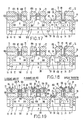
- Figs. 1-19 comprise sectional views illustrating successive process steps in constructing a BICMOS semiconductor device in accordance with the present invention, with Figs. 11A and 14A comprising top views of the immediately preceding sectional view.
- The following detailed description of the invention is directed to a process of fabricating a BICMOS device including a pair of N- and P- channel enhancement mode CMOS devices and an NPN bipolar transistor. It will be understood that the particular conductivity types and concentrations described herein are exemplary in nature. Through the reversal of conductivity types and/or the appropriate adjustment of conductivity concentrations, it will be apparent to those skilled in the art that the present invention can be used to fabricate CMOS devices of differing concentrations and/or a PNP-type bipolar transistor. It will also be understood that the present invention is not limited to the fabrication of BICMOS devices, but has utility in the fabrication of separate bipolar and insulated gate devices, as well as in the fabrication of other types of semiconductor devices requiring closely spaced, highly aligned device regions.
- Referring now to Fig. 1, a wafer or
substrate 10 of P-silicon monocrystalline material is provided, preferably having a <100> crystallographic orientation and a resistivity in the range of 10-20 ohms-centimeter. AnN+ subcollector region 12 is formed insubstrate 10, for example by a conventional process of implanting arsenic (As) ions to a concentration in the range of about 1x10¹⁹-1x10²⁰ atoms/cm³. Alternatively,N+ subcollector region 12 can be formed by conventional diffusion processes. - Referring now to Fig. 2, a P-
epitaxial layer 14 is grown onlayer 12, for example using a conventional low temperature, low pressure silicon epitaxial process.Layer 14 is preferably formed to a thickness in the range of about 0.6-1.5 microns. - Examining now Fig. 3, a pair of N
well regions layer 14 so as to bound an undisturbed P-well region 14B.Regions layer 14 using standard photolithographic masking processes to block outregion 14B.Regions - Referring now to Fig. 4, four
deep isolation regions wells deep isolation region layer 12, and a shallow T-cap at the surface of the device extending partway into the adjoining wells. Adjacentdeep isolation regions well 14A. Similarly, adjacentdeep isolation regions wells shallow isolation region 24 is formed at the surface of well 14C, spaced laterally from the T-cap ofisolation region 20 to electrically isolate subsequently formed elements of a bipolar transistor.Isolation region 24 is spaced, for example, a distance D1 in the range of about 1-10 microns from the cap ofdeep isolation region 20, and extends down into well 14C. - Shallow
isolation region 24, as well as the T-caps ofdeep isolation regions deep isolation regions - Referring now to Fig. 5, an N+
subcollector reachthrough region 28 is formed betweenisolation regions subcollector layer 12.Region 28 is formed, for example, by a conventional process of diffusing POCl₃ into well 14C betweenisolation regions subcollector reachthrough region 28, and forms anoxide layer 34 on the surface of the device.Oxide layer 34 is formed, for example, to a thickness of about 100-500 Angstroms, the layer being appreciably thicker at the surface of subcollector reachthroughregion 28. - Referring still to Fig. 5, the surface conductivities of
wells well 14A, for example, depending on whether the transistor is desired to operate in an enhancement or depletion mode, boron or phosphorous ions, or both, are selectively implanted shallowly into the surface of the well to form aregion 30 with a dosage in the range of about 1-1Ox1O¹²/cm². For the N-channel MOSFET to be formed inwell 14B, for example, boron ions are selectively implanted shallowly into the surface of the well to a dosage in the range of about 1-5x10¹²/cm². - Referring now to Fig. 6, a
layer 36 of conductive material is formed overlayer 34. For the purposes of the present invention, suitable conductive materials forlayer 36 include high-temperature, high-conductivity conductor such as conductive polysilicon, polycide (comprising polysilicon with a metal silicide coating), and refractory metals such as tungsten silicide (WSi₂). In a preferred embodiment of the invention,layer 36 comprises an intrinsic (non-doped) polycrystalline silicon (polysilicon) formed by a conventional chemical vapor deposition (CVD) process to a thickness in then range of about 2,000-6,000 Angstroms. - Subsequent to the formation of
layer 36,regions wells region 37B oflayer 36, overlying well 14B, is doped to P+ using conventional, selective boron ion implantation. Alternatively, if it is desired to simplify the fabrication process,polysilicon layer 36 can be formed in situ doped to an N+ concentration in the range of not less than 2x10²⁰ atoms/cm³. - Subsequent to the formation of
layer 36, anoptional layer 38 of silicon dioxide can be formed thereon by a conventional CVD process. When used,layer 38 is preferably formed to a thickness of about 100-500 Angstroms, and functions to facilitate the delineation of the studs described below, and to relieve interlayer stresses betweenlayer 36 and a subsequently formednitride layer 40.Nitride layer 40 is formed, for example, by a conventional CVD process to a thickness in the range of about 1,000-2,000 Angstroms. - Subsequent to the formation of
layers mask regions Mask regions 42, 44 are centered over regions inwells 14AMask region 46 is centered over the surface of well 14C (i.e. the surface between the edges ofisolation regions 22, 24), a region which will subsequently form the emitter of a completed bipolar transistor. - Referring now to Fig. 7, the portions of
layers mask regions underlying oxide layer 34. Appropriate RIE etchants include: CF₄+O₂ to removesilicon nitride layer 40; CF₄+H₂ to removesilicon dioxide layer 38; and Cl₂+Ar or CF₄+O₂ to removepolysilicon layer 36. The resistmask regions studs wells layer 36 performed as described above, the portions of the layer remaining instuds layer 36 had been formed in situ doped N+ in accordance with the alternate embodiment described above, these same portions would be doped to N+. - Referring now to Fig. 8,
oxide layer 34 outside the regions ofstuds layer 38 was thicker at the surface of subcollector reachthrough 28 than over the remainder of the device surface, aprotective portion 60 of the oxide remains after the above-described etch. Subsequent to the removal oflayer 34, aphotolithographic blocking mask 61 is formed over the surface of the device betweenisolation regions well 14B. A conventional, blanket boron ion implantation is then performed with a dose in the range of 1x10¹² atoms/cm³ to 1x10¹³ atoms/cm³. This boron ion implantation converts the surface region ofwell 14A not underneathstud 48 into P type lightly doped drain (LDD)regions well 14C not underneathstud 52 into P type intrinsic/extrinsic base link-upregion 58. - As shown in Fig. 9, a pair of photolithographic blocking masks 63, 65 are formed over
wells well 14B not underneathstud 50 into Ntype LDD regions - Referring now to Fig. 11, subsequent to the completion of the various ion implantations to form the above-described LDD and link-up regions, silicon dioxide sidewalls 62 are formed on the sides of each of
studs stud 48 is designated with the suffix A, the sidewall formed onstud 50 is designated with the suffix C, and the sidewall formed aboutstud 52 is indicated with the suffix E. From a consideration of the top view in Fig. 11A, it will be appreciated thatstuds LDD regions studs Stud 52, however, is situated with its sidewall 62B entirely within what will be the active region of the subsequently formed bipolar transistor. Link-upregion 58 thus comprises a unitary electricalregion surrounding stud 58. - Sidewalls 62 are formed, for example, by first using a conventional CVD process to form a conformal layer of SiO₂ (not shown) to a thickness in the range of about 1,000-5,000 Angstroms. Subsequent to the formation of this conformal layer of SiO₂, an anisotropic RIE etchant such as CF₄ + O₂ is used to remove the horizontal portions of the layer, leaving vertical sidewalls 62.
- Referring now to Fig. 12, a
layer 64 of polycide with accompanyingmetal silicide surface 64A is deposited conformally over the top of the device to a thickness D2 of at least the vertical height of sidewalls 62, or since the sidewalls cover the vertical surfaces ofstuds Layer 64 is formed, for example, by a conventional low pressure CVD process. - Subsequent to the formation of
layer 64, the layer is planarized evenly with the tops of sidwalls 62 andstuds - An exemplary photoresist reflow and RIE etch-back process is shown in the article "A Practical Trench Isolation Technology with a Novel Planarization Process", to Fuse et al., IEDM 1987, pgs. 732-734 (incorporated herein by reference). Briefly, the article describes a process wherein large valleys in the SiO₂ are filled with a first photoresist. A thin layer of SiO₂ is sputtered over the entire device, and a planarizing layer of second photoresist deposited over the sputtered SiO₂. The second photoresist is etched to the surface of the sputter-deposited SiO₂. The sputter-deposited SiO₂, resist films, and underlying SiO₂ are subsequently etched to the desired height with a gas of CHF₃, C₂F₆, and O₂.
- After the planarization of
layer 64,regions 64B oflayer 64 surroundingstud 50 are selectively doped with arsenic (As), whileregions 64C oflayer 64 surroundingstuds regions - Referring now to Figs. 14, 14A,
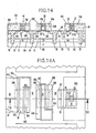
layer 64 is delineated to form five discrete regions which, for purposes of explanation, are indicated byreference numbers region 70 forming a rectangular ring aboutstud 52 andsidewall 62E.Regions stud 48, the former overlyingLDD implant region 54A and the latter extending from the edge ofisolation trench 18 to overlieLDD implant region 54B.Regions stud 50, with the former extending from an edge ofisolation trench 18 to overlieLDD implant region 56A, and the latter extending from an edge ofisolation region 20 to overlieLDD implant region 56B.Region 70 forms a ring about the sidewalls ofstud 52, with the left half (as viewed in the Figs.) extending from an edge ofisolation trench 24 to overlie intrinsic-extrinsic base link-upregion 58, and the right half extending from an edge ofisolation trench 22 to overlie the other side of the link-up region. - The delineation of
layer 64 to formregions 66, 68, and 70 as shown in Fig. 14 is accomplished, for example, by the use of an appropriate RIE etchant such as CF₄ + H₂ in combination with conventional photolithographic masking. - Referring now to Fig. 15, subsequent to the delineation of
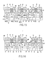
regions layer 72 of SiO₂ over the exposed surfaces of these regions to a thickness in the range of about 1,000-5,000 Angstroms.Layer 72 is not formed, of course, over the exposed surfaces of the device or over the tops ofstuds regions drain regions drain regions extrinsic base region 58. - Referring now to Fig. 16,
stud 52 over well 14C is removed to leavesidewall 62E bounding an exposed area on the well surface.Stud 52 is removed by firstetching nitride layer 40 with a CF₄/O₂ plasma etch or a hot bath of phosphoric acid (H₃PO₄). The relativelythin layer 38 of silicon dioxide is removed by dipping in BHF without substantially disturbing the muchthicker layer 72 andsidewall 62E of silicon dioxide.Polysilicon layer 36 is removed, for example, with a pyrocathecal etch, andsilicon dioxide layer 34 is removed with BHF. It will be appreciated that the step of removingsilicon dioxide layer 34 with a BHF dip etch can be carefully controlled to stop at the surface ofwell 14C so as not to etch into the device surface or otherwise disturb the nature of the subsequently formed bipolar transistor. - Subsequent to the removal of
stud 52, a buriedsubcollector implant region 74 is formed inwell 14C by a conventional implantation of arsenic or phosphorus ions. Because the remainder of the device is masked bypolysilicon regions layer 72, andstuds sidewall 62E by the removal ofstud 52. The surface of subcollector reachthrough 28 is exposed to the implantation. However, the dopant concentration of subcollector reachthroughregion 28 is sufficiently larger than that ofsubcollector region 74 so it is not appreciably altered. - Following the formation of buried
subcollector region 74, a conventional, blanket implantation of Boron ions if performed with a dose in the range of 1-10x10¹² atoms/cm² to form anintrinsic base region 75. - After the formation of
intrinsic base region 75, a conventional, blanket implantation of Arsenic ions is performed with a dose in the range of 1-10x10¹⁵ atoms/cm² to form anemitter region 76. Alternatively,emitter region 76 can be out-diffused from the emitter polysilicon deposited as described hereinbelow, or from a combination of both of these processes. It will be understood that buriedregion 74,intrinsic base region 75, andemitter region 76 can be formed in interchangeable order. - In each of the above-described implantation steps, the
polysilicon regions layer 72, andstuds region 28 is sufficiently high that it is left effectively undisturbed. - Referring now to Fig. 17, a
layer 80 of in situ arsenic doped polysilicon, having a concentration in the range of about 1-10x10²⁰ atoms/cm³, is formed over the exposed inner surface ofsidewall 62E andoverlying emitter region 76. Subsequent to the formation oflayer 80, alayer 82 of metal silicide is formed thereover in the manner shown in Fig. 18 to increase the conductivity oflayer 80. Alternately,layer 80 can comprise an intrinsic polysilicon later doped by a conventional implantation with arsenic ions to a concentration in the range of about 1-10x10²⁰ atoms/cm³.Layer 80 is formed, for example, by a low pressure CVD process.Layer 82 is formed, for example, by physically evaporating or sputtering a thin layer of metal, for example titanium, overlayer 80, and converting it into a metal silicide using an alloy sintering anneal. If it is desired to formemitter region 75 from, or increase the concentration of the emitter region by out-diffusion fromlayer 80, then an emitter dopant drive-in anneal, in a temperature range of about 800-950 degrees centigrade, is performed prior to the formation oflayer 82. - Continuing to describe Fig. 18, the nitride cap layers 40 on the tops of
studs studs 48′, 50′, respectively. - Referring now to Fig. 19, conventional processes are used to form contact holes 84, 86, 88, 90, and 92 through
layer 72 to expose surface areas ofpolysilicon regions metal interconnections Metal contacts Metal contacts 96 and 102overlie polysilicon layer 38 instuds 48′, 50′, respectively.Metal contact 106 spansisolation regions region 28, andmetal contact 108 overliespolycide layer 82 overwell 14C. Each of the metal interconnections described above makes ohmic electrical contact with the underlying, contacted region. - In accordance with the above-described embodiment of the invention, there has thus been formed an N-channel MOSFET in the region of isolated device well 14A, a P-channel MOSFET in the region of
isolated device well 14B, and a vertically disposed NPN bipolar transistor in the region of isolated device well 14C.Metal contacts Metal contacts metal contacts studs polysilicon layer 64 to formdevice contact regions device contact regions - There is thus provided a BICMOS logic circuit and a method of forming the same. The circuit includes densely packed, high-speed devices formed by a combination of reverse image and self-aligned process steps. The process used to form the BICMOS logic circuit is readily adaptable to the formation of other types of logic circuits, including exclusive bipolar or CMOS devices, and other semiconductor devices which can benefit from the self-alignment techniques of the present invention. The process has particular industrial application in the formation of highly integrated logic circuits.
- While the present invention has been shown and described with respect to particular embodiments, numerous changes, modifications, and improvements will occur to those skilled in the art without departing from the scope and spirit of the invention.
Claims (19)
forming a stud over said body;
forming a sidewall of insulating material on said stud;
forming a layer of conductive material generally conformally over said body, said stud, and said sidewall to a depth at least equal to the height of said sidewall; and
planarizing said layer of conductive material to a height equal to or less than the height of said sidewall, whereby to form a device contact.
forming a first layer of material over said first doped region;
forming a second layer of conductive material over said first layer;
forming a third layer of insulating material over said second layer; and
removing portions of said first, second, and third layers to delineate said stud.
said first layer comprises an oxide;
said second layer comprises a doped polysilicon, a refractory metal, or a metal silicide; and
said third layer comprises a nitride.
forming a planarizing layer over said layer of conductive material; and
etching said planarizing and conductive layers.
forming a layer of insulating material generally conformally over said semiconductor body and said stud; and
anisotropically etching said layer of insulating material to leave said sidewall.
removing said stud while leaving said sidewall to expose a portion of said first doped region.
forming a stud over said first doped region;
forming a sidewall of an insulative material about the periphery of said stud;
removing said stud while leaving said sidewall to expose a portion of said first doped region; and
using said sidewall as a mask to form an intrinsic base region of a second conductivity type in the exposed portion of said first doped region;
providing a body of semiconductor material including at least first and second adjacent electrically isolated device regions of opposite conductivity types;
forming first and second studs over said first and second device regions, respectively, such that said first and second studs bisect said first and second device regions, each of said studs comprising a layer of insulating material overlain by a layer of conductive material, the conductive layer in each of said studs of same conductivity type as the underlying device region;
using said first and second studs as masks to form first and second doped regions adjoining opposite sides of said studs in said first and second device regions, respectively, each of said first and second doped regions of opposite conductivity type to its associated device region;
forming insulating sidewalls on each of said first and second studs; and
forming an electrical contact on the conductive layer each of said studs.
providing a body of semiconductor material including first, second and third electrically isolated device regions said first and second device regions adjacent each other and of opposite conductivity types;
forming first, second, and third studs over said first, second, and third device regions, respectively, such that said first and second studs bisect said first and second device regions;
using said first and second studs as masks to form first and second doped regions adjoining opposite sides of said first and second studs in each of said first and second device regions, respectively, each of said first and second doped regions of opposite conductivity type to its associated device region;
forming first, second, and third insulating sidewalls on said first, second, and third studs, respectively;
removing said third stud while leaving the sidewall associated with said third stud to expose a portion of said third device region.
Applications Claiming Priority (2)
| Application Number | Priority Date | Filing Date | Title |
|---|---|---|---|
| US07/261,952 US5015594A (en) | 1988-10-24 | 1988-10-24 | Process of making BiCMOS devices having closely spaced device regions |
| US261952 | 1988-10-24 |
Publications (3)
| Publication Number | Publication Date |
|---|---|
| EP0366587A2 true EP0366587A2 (en) | 1990-05-02 |
| EP0366587A3 EP0366587A3 (en) | 1991-04-17 |
| EP0366587B1 EP0366587B1 (en) | 1995-05-24 |
Family
ID=22995583
Family Applications (1)
| Application Number | Title | Priority Date | Filing Date |
|---|---|---|---|
| EP89480155A Expired - Lifetime EP0366587B1 (en) | 1988-10-24 | 1989-09-26 | Semiconductor devices having closely spaced device regions formed using a self aligning reverse image fabrication process |
Country Status (5)
| Country | Link |
|---|---|
| US (1) | US5015594A (en) |
| EP (1) | EP0366587B1 (en) |
| JP (1) | JPH07105457B2 (en) |
| CA (1) | CA1300764C (en) |
| DE (1) | DE68922817T2 (en) |
Cited By (4)
| Publication number | Priority date | Publication date | Assignee | Title |
|---|---|---|---|---|
| EP0495329A2 (en) * | 1991-01-18 | 1992-07-22 | International Business Machines Corporation | High performance/high density bicmos process |
| EP0538054A1 (en) * | 1991-10-16 | 1993-04-21 | Nec Corporation | Semiconductor integrate circuit device having N- and P- type insulated-gate field effect transistors and its production method |
| EP0809302A2 (en) * | 1996-05-22 | 1997-11-26 | International Business Machines Corporation | CMOS structure in isolated wells with merged depletion regions and method of making same |
| EP2053638A3 (en) * | 1999-12-08 | 2009-07-29 | Samsung Electronics Co., Ltd | Semiconductor device having a self-aligned contact structure and methods of forming the same |
Families Citing this family (61)
| Publication number | Priority date | Publication date | Assignee | Title |
|---|---|---|---|---|
| US5223449A (en) * | 1989-02-16 | 1993-06-29 | Morris Francis J | Method of making an integrated circuit composed of group III-V compound field effect and bipolar semiconductors |
| US5138420A (en) * | 1989-11-24 | 1992-08-11 | Mitsubishi Denki Kabushiki Kaisha | Semiconductor device having first and second type field effect transistors separated by a barrier |
| US5234847A (en) * | 1990-04-02 | 1993-08-10 | National Semiconductor Corporation | Method of fabricating a BiCMOS device having closely spaced contacts |
| JPH03286562A (en) * | 1990-04-03 | 1991-12-17 | Oki Electric Ind Co Ltd | Semiconductor device and its manufacture |
| US5198374A (en) * | 1990-04-03 | 1993-03-30 | Oki Electric Industry Co., Ltd. | Method of making biCMOS integrated circuit with shallow N-wells |
| US5102809A (en) * | 1990-10-11 | 1992-04-07 | Texas Instruments Incorporated | SOI BICMOS process |
| US5202591A (en) * | 1991-08-09 | 1993-04-13 | Hughes Aircraft Company | Dynamic circuit disguise for microelectronic integrated digital logic circuits |
| JP3175973B2 (en) * | 1992-04-28 | 2001-06-11 | 株式会社東芝 | Semiconductor device and method of manufacturing the same |
| US5376816A (en) * | 1992-06-24 | 1994-12-27 | Nec Corporation | Bi-cmos integrated circuit device having buried region use in common for bipolar and mos transistors |
| US5407841A (en) * | 1992-10-30 | 1995-04-18 | Hughes Aircraft Company | CBiCMOS fabrication method using sacrificial gate poly |
| JPH07169771A (en) * | 1993-12-15 | 1995-07-04 | Nec Corp | Semiconductor device and its manufacture |
| US5376578A (en) * | 1993-12-17 | 1994-12-27 | International Business Machines Corporation | Method of fabricating a semiconductor device with raised diffusions and isolation |
| KR0137974B1 (en) * | 1994-01-19 | 1998-06-15 | 김주용 | Semiconductor device & process for manufacturing the same |
| US5604159A (en) | 1994-01-31 | 1997-02-18 | Motorola, Inc. | Method of making a contact structure |
| KR0120572B1 (en) * | 1994-05-04 | 1997-10-20 | 김주용 | Semiconductor device and manufacture of the same |
| KR0131723B1 (en) * | 1994-06-08 | 1998-04-14 | 김주용 | Manufacturing method for semiconductor device |
| US5432105A (en) * | 1994-09-19 | 1995-07-11 | United Microelectronics Corporation | Method for fabricating self-aligned polysilicon contacts on FET source/drain areas |
| US6445043B1 (en) * | 1994-11-30 | 2002-09-03 | Agere Systems | Isolated regions in an integrated circuit |
| JPH08172100A (en) * | 1994-12-16 | 1996-07-02 | Mitsubishi Electric Corp | Semiconductor device |
| US5571733A (en) * | 1995-05-12 | 1996-11-05 | Micron Technology, Inc. | Method of forming CMOS integrated circuitry |
| KR0155536B1 (en) * | 1995-06-24 | 1998-10-15 | 양승택 | Method of fabricating bicmos device |
| US5627097A (en) * | 1995-07-03 | 1997-05-06 | Motorola, Inc. | Method for making CMOS device having reduced parasitic capacitance |
| US5637525A (en) * | 1995-10-20 | 1997-06-10 | Micron Technology, Inc. | Method of forming a CMOS circuitry |
| US5718800A (en) * | 1995-11-08 | 1998-02-17 | Micron Technology, Inc. | Self-aligned N+/P+ doped polysilicon plugged contacts to N+/P+ doped polysilicon gates and to N+/P+ doped source/drain regions |
| FR2756103B1 (en) * | 1996-11-19 | 1999-05-14 | Sgs Thomson Microelectronics | MANUFACTURE OF BIPOLAR / CMOS INTEGRATED CIRCUITS AND A CAPACITOR |
| FR2756104B1 (en) * | 1996-11-19 | 1999-01-29 | Sgs Thomson Microelectronics | MANUFACTURE OF BIPOLAR / CMOS INTEGRATED CIRCUITS |
| FR2756100B1 (en) | 1996-11-19 | 1999-02-12 | Sgs Thomson Microelectronics | BIPOLAR TRANSISTOR WITH INHOMOGENEOUS TRANSMITTER IN A BICMOS INTEGRATED CIRCUIT |
| FR2756101B1 (en) * | 1996-11-19 | 1999-02-12 | Sgs Thomson Microelectronics | METHOD FOR MANUFACTURING AN NPN TRANSISTOR IN BICMOS TECHNOLOGY |
| US5874328A (en) * | 1997-06-30 | 1999-02-23 | Advanced Micro Devices, Inc. | Reverse CMOS method for dual isolation semiconductor device |
| US5937287A (en) | 1997-07-22 | 1999-08-10 | Micron Technology, Inc. | Fabrication of semiconductor structures by ion implantation |
| US6177339B1 (en) * | 1998-08-27 | 2001-01-23 | Micron Technology, Inc. | Semiconductor processing methods of forming integrated circuitry and semiconductor processing methods of forming dynamic random access memory (DRAM) circuitry |
| US6395623B1 (en) * | 1998-08-27 | 2002-05-28 | Micron Technology, Inc. | Semiconductor processing methods of forming a contact opening to a conductive line and methods of forming substrate active area source/drain regions |
| US6331481B1 (en) | 1999-01-04 | 2001-12-18 | International Business Machines Corporation | Damascene etchback for low ε dielectric |
| US6399993B1 (en) | 1999-07-07 | 2002-06-04 | Matsushita Electric Industrial Co., Ltd. | Semiconductor device and method for fabricating the same |
| JP2001085442A (en) * | 1999-09-09 | 2001-03-30 | Mitsubishi Electric Corp | Semiconductor device with transistor |
| WO2001020664A1 (en) * | 1999-09-17 | 2001-03-22 | Telefonaktiebolaget Lm Ericsson | A self-aligned method for forming deep trenches in shallow trenches for isolation of semiconductor devices |
| JP2002237575A (en) * | 2001-02-08 | 2002-08-23 | Sharp Corp | Semiconductor device and its manufacturing method |
| SE0103036D0 (en) * | 2001-05-04 | 2001-09-13 | Ericsson Telefon Ab L M | Semiconductor process and integrated circuit |
| US6492238B1 (en) | 2001-06-22 | 2002-12-10 | International Business Machines Corporation | Bipolar transistor with raised extrinsic base fabricated in an integrated BiCMOS circuit |
| US6566208B2 (en) * | 2001-07-25 | 2003-05-20 | Chartered Semiconductor Manufacturing Ltd. | Method to form elevated source/drain using poly spacer |
| US6927476B2 (en) | 2001-09-25 | 2005-08-09 | Internal Business Machines Corporation | Bipolar device having shallow junction raised extrinsic base and method for making the same |
| JP4531343B2 (en) * | 2003-03-26 | 2010-08-25 | 株式会社半導体エネルギー研究所 | Driving circuit |
| US6809024B1 (en) | 2003-05-09 | 2004-10-26 | International Business Machines Corporation | Method to fabricate high-performance NPN transistors in a BiCMOS process |
| US6777302B1 (en) * | 2003-06-04 | 2004-08-17 | International Business Machines Corporation | Nitride pedestal for raised extrinsic base HBT process |
| US6936522B2 (en) * | 2003-06-26 | 2005-08-30 | International Business Machines Corporation | Selective silicon-on-insulator isolation structure and method |
| US20050179111A1 (en) * | 2004-02-12 | 2005-08-18 | Iwen Chao | Semiconductor device with low resistive path barrier |
| KR101118652B1 (en) * | 2004-12-17 | 2012-03-07 | 삼성전자주식회사 | Bipolar Junction Transistor with high Gain integratable with CMOS FET process and Method for Forming the Same |
| US20070158779A1 (en) * | 2006-01-12 | 2007-07-12 | International Business Machines Corporation | Methods and semiconductor structures for latch-up suppression using a buried damage layer |
| US7648869B2 (en) * | 2006-01-12 | 2010-01-19 | International Business Machines Corporation | Method of fabricating semiconductor structures for latch-up suppression |
| US7491618B2 (en) * | 2006-01-26 | 2009-02-17 | International Business Machines Corporation | Methods and semiconductor structures for latch-up suppression using a conductive region |
| US7276768B2 (en) * | 2006-01-26 | 2007-10-02 | International Business Machines Corporation | Semiconductor structures for latch-up suppression and methods of forming such semiconductor structures |
| US20070194403A1 (en) * | 2006-02-23 | 2007-08-23 | International Business Machines Corporation | Methods for fabricating semiconductor device structures with reduced susceptibility to latch-up and semiconductor device structures formed by the methods |
| US7754513B2 (en) * | 2007-02-28 | 2010-07-13 | International Business Machines Corporation | Latch-up resistant semiconductor structures on hybrid substrates and methods for forming such semiconductor structures |
| US7818702B2 (en) * | 2007-02-28 | 2010-10-19 | International Business Machines Corporation | Structure incorporating latch-up resistant semiconductor device structures on hybrid substrates |
| US7808055B2 (en) * | 2007-06-21 | 2010-10-05 | Gigadevice Semiconductor Inc. | Methods and apparatus for semiconductor memory devices manufacturable using bulk CMOS process manufacturing |
| US7812367B2 (en) * | 2008-10-15 | 2010-10-12 | Semiconductor Components Industries, Llc | Two terminal low capacitance multi-channel ESD device |
| US8039326B2 (en) * | 2009-08-20 | 2011-10-18 | Globalfoundries Inc. | Methods for fabricating bulk FinFET devices having deep trench isolation |
| US8581347B2 (en) * | 2010-07-22 | 2013-11-12 | Taiwan Semiconductor Manufacturing Company, Ltd. | Forming bipolar transistor through fast EPI-growth on polysilicon |
| US9401410B2 (en) * | 2014-11-26 | 2016-07-26 | Texas Instruments Incorporated | Poly sandwich for deep trench fill |
| US20160372360A1 (en) * | 2015-06-17 | 2016-12-22 | Taiwan Semiconductor Manufacturing Co., Ltd. | Semiconductor structure with junction leakage reduction |
| CN114695113A (en) * | 2020-12-28 | 2022-07-01 | 芯恩(青岛)集成电路有限公司 | BiCMOS device and manufacturing method of heterojunction bipolar transistor therein |
Citations (7)
| Publication number | Priority date | Publication date | Assignee | Title |
|---|---|---|---|---|
| US4252579A (en) * | 1979-05-07 | 1981-02-24 | International Business Machines Corporation | Method for making single electrode U-MOSFET random access memory utilizing reactive ion etching and polycrystalline deposition |
| EP0078890A2 (en) * | 1981-11-06 | 1983-05-18 | Rockwell International Corporation | Method of fabrication of dielectrically isolated CMOS device with an isolated slot |
| US4551911A (en) * | 1982-12-28 | 1985-11-12 | Tokyo Shibaura Denki Kabushiki Kaisha | Method for manufacturing semiconductor device |
| US4593459A (en) * | 1984-12-28 | 1986-06-10 | Gte Laboratories Incorporated | Monolithic integrated circuit structure and method of fabrication |
| EP0226890A1 (en) * | 1985-12-17 | 1987-07-01 | Siemens Aktiengesellschaft | Method for the fabrication of self-aligned bipolar transistor structures with reduced base resistance |
| EP0233791A2 (en) * | 1986-02-21 | 1987-08-26 | SGS Microelettronica SpA | Insulated gate field effect transistor and method of manufacture thereof |
| US4774204A (en) * | 1987-06-02 | 1988-09-27 | Texas Instruments Incorporated | Method for forming self-aligned emitters and bases and source/drains in an integrated circuit |
Family Cites Families (10)
| Publication number | Priority date | Publication date | Assignee | Title |
|---|---|---|---|---|
| US4608589A (en) * | 1980-07-08 | 1986-08-26 | International Business Machines Corporation | Self-aligned metal structure for integrated circuits |
| JPS60128656A (en) * | 1983-12-16 | 1985-07-09 | Hitachi Ltd | Semiconductor device |
| US4808548A (en) * | 1985-09-18 | 1989-02-28 | Advanced Micro Devices, Inc. | Method of making bipolar and MOS devices on same integrated circuit substrate |
| US4686763A (en) * | 1985-10-02 | 1987-08-18 | Advanced Micro Devices, Inc. | Method of making a planar polysilicon bipolar device |
| DE3767431D1 (en) * | 1986-04-23 | 1991-02-21 | American Telephone & Telegraph | METHOD FOR PRODUCING SEMICONDUCTOR COMPONENTS. |
| JPH0628266B2 (en) * | 1986-07-09 | 1994-04-13 | 株式会社日立製作所 | Method for manufacturing semiconductor device |
| JP2581548B2 (en) * | 1986-10-13 | 1997-02-12 | 株式会社日立製作所 | Method for manufacturing semiconductor device |
| US4745087A (en) * | 1987-01-13 | 1988-05-17 | Advanced Micro Devices, Inc. | Method of making fully self-aligned bipolar transistor involving a polysilicon collector contact formed in a slot with an oxide sidewall |
| JP2633559B2 (en) * | 1987-03-31 | 1997-07-23 | 株式会社東芝 | Method for manufacturing bipolar CMOS semiconductor device |
| US4800171A (en) * | 1987-10-02 | 1989-01-24 | Advanced Micro Devices, Inc. | Method for making bipolar and CMOS integrated circuit structures |
-
1988
- 1988-10-24 US US07/261,952 patent/US5015594A/en not_active Expired - Lifetime
-
1989
- 1989-06-12 CA CA000602547A patent/CA1300764C/en not_active Expired - Fee Related
- 1989-09-26 EP EP89480155A patent/EP0366587B1/en not_active Expired - Lifetime
- 1989-09-26 DE DE68922817T patent/DE68922817T2/en not_active Expired - Fee Related
- 1989-10-19 JP JP1270502A patent/JPH07105457B2/en not_active Expired - Lifetime
Patent Citations (7)
| Publication number | Priority date | Publication date | Assignee | Title |
|---|---|---|---|---|
| US4252579A (en) * | 1979-05-07 | 1981-02-24 | International Business Machines Corporation | Method for making single electrode U-MOSFET random access memory utilizing reactive ion etching and polycrystalline deposition |
| EP0078890A2 (en) * | 1981-11-06 | 1983-05-18 | Rockwell International Corporation | Method of fabrication of dielectrically isolated CMOS device with an isolated slot |
| US4551911A (en) * | 1982-12-28 | 1985-11-12 | Tokyo Shibaura Denki Kabushiki Kaisha | Method for manufacturing semiconductor device |
| US4593459A (en) * | 1984-12-28 | 1986-06-10 | Gte Laboratories Incorporated | Monolithic integrated circuit structure and method of fabrication |
| EP0226890A1 (en) * | 1985-12-17 | 1987-07-01 | Siemens Aktiengesellschaft | Method for the fabrication of self-aligned bipolar transistor structures with reduced base resistance |
| EP0233791A2 (en) * | 1986-02-21 | 1987-08-26 | SGS Microelettronica SpA | Insulated gate field effect transistor and method of manufacture thereof |
| US4774204A (en) * | 1987-06-02 | 1988-09-27 | Texas Instruments Incorporated | Method for forming self-aligned emitters and bases and source/drains in an integrated circuit |
Non-Patent Citations (1)
| Title |
|---|
| Semiconductor Devices, S.M. Sze, J.Wiley and Sons. * |
Cited By (6)
| Publication number | Priority date | Publication date | Assignee | Title |
|---|---|---|---|---|
| EP0495329A2 (en) * | 1991-01-18 | 1992-07-22 | International Business Machines Corporation | High performance/high density bicmos process |
| EP0495329A3 (en) * | 1991-01-18 | 1992-09-16 | International Business Machines Corporation | High performance/high density bicmos process |
| EP0538054A1 (en) * | 1991-10-16 | 1993-04-21 | Nec Corporation | Semiconductor integrate circuit device having N- and P- type insulated-gate field effect transistors and its production method |
| EP0809302A2 (en) * | 1996-05-22 | 1997-11-26 | International Business Machines Corporation | CMOS structure in isolated wells with merged depletion regions and method of making same |
| EP0809302A3 (en) * | 1996-05-22 | 1998-12-30 | International Business Machines Corporation | CMOS structure in isolated wells with merged depletion regions and method of making same |
| EP2053638A3 (en) * | 1999-12-08 | 2009-07-29 | Samsung Electronics Co., Ltd | Semiconductor device having a self-aligned contact structure and methods of forming the same |
Also Published As
| Publication number | Publication date |
|---|---|
| JPH07105457B2 (en) | 1995-11-13 |
| US5015594A (en) | 1991-05-14 |
| EP0366587A3 (en) | 1991-04-17 |
| EP0366587B1 (en) | 1995-05-24 |
| DE68922817T2 (en) | 1995-11-30 |
| JPH02164059A (en) | 1990-06-25 |
| DE68922817D1 (en) | 1995-06-29 |
| CA1300764C (en) | 1992-05-12 |
Similar Documents
| Publication | Publication Date | Title |
|---|---|---|
| US5015594A (en) | Process of making BiCMOS devices having closely spaced device regions | |
| EP0088922B1 (en) | A method of forming electrodes and wiring strips on a semiconductor device | |
| US5693974A (en) | Elevated source/drain with solid phase diffused source/drain extension for deep sub-micron MOSFETS | |
| CA2024640C (en) | Bicmos process | |
| US4752589A (en) | Process for the production of bipolar transistors and complementary MOS transistors on a common silicon substrate | |
| US4839305A (en) | Method of making single polysilicon self-aligned transistor | |
| US4897703A (en) | Recessed contact bipolar transistor and method | |
| US5171702A (en) | Method for forming a thick base oxide in a BiCMOS process | |
| US4745087A (en) | Method of making fully self-aligned bipolar transistor involving a polysilicon collector contact formed in a slot with an oxide sidewall | |
| US4985744A (en) | Method for forming a recessed contact bipolar transistor and field effect transistor | |
| US4962053A (en) | Bipolar transistor fabrication utilizing CMOS techniques | |
| US5075241A (en) | Method of forming a recessed contact bipolar transistor and field effect device | |
| CA1241458A (en) | Side-etching method of making bipolar transistor | |
| US4735911A (en) | Process for the simultaneous production of bipolar and complementary MOS transistors on a common silicon substrate | |
| EP0236687B1 (en) | Self-aligned p contact diffusion | |
| JPH05198752A (en) | Mos device and manufacture of semiconductor structure with bipolar-device | |
| EP0421507A2 (en) | Method of manufacturing a bipolar transistor | |
| EP0281235B1 (en) | Bipolar transistor fabrication utilizing cmos techniques | |
| US5164801A (en) | A p channel mis type semiconductor device | |
| EP0637838A2 (en) | Integrated circuit with self-aligned isolation | |
| US5352617A (en) | Method for manufacturing Bi-CMOS transistor devices | |
| US5266505A (en) | Image reversal process for self-aligned implants in planar epitaxial-base bipolar transistors | |
| US5065209A (en) | Bipolar transistor fabrication utilizing CMOS techniques | |
| US5606192A (en) | Semiconductor integrated circuits having bipolar transistors and LDD-structured MOSFET | |
| EP0403009B1 (en) | A method of manufacturing a semiconductor device |
Legal Events
| Date | Code | Title | Description |
|---|---|---|---|
| PUAI | Public reference made under article 153(3) epc to a published international application that has entered the european phase |
Free format text: ORIGINAL CODE: 0009012 |
|
| AK | Designated contracting states |
Kind code of ref document: A2 Designated state(s): DE FR GB IT |
|
| 17P | Request for examination filed |
Effective date: 19900820 |
|
| PUAL | Search report despatched |
Free format text: ORIGINAL CODE: 0009013 |
|
| AK | Designated contracting states |
Kind code of ref document: A3 Designated state(s): DE FR GB IT |
|
| 17Q | First examination report despatched |
Effective date: 19931008 |
|
| GRAA | (expected) grant |
Free format text: ORIGINAL CODE: 0009210 |
|
| AK | Designated contracting states |
Kind code of ref document: B1 Designated state(s): DE FR GB IT |
|
| PG25 | Lapsed in a contracting state [announced via postgrant information from national office to epo] |
Ref country code: IT Free format text: LAPSE BECAUSE OF FAILURE TO SUBMIT A TRANSLATION OF THE DESCRIPTION OR TO PAY THE FEE WITHIN THE PRESCRIBED TIME-LIMIT;WARNING: LAPSES OF ITALIAN PATENTS WITH EFFECTIVE DATE BEFORE 2007 MAY HAVE OCCURRED AT ANY TIME BEFORE 2007. THE CORRECT EFFECTIVE DATE MAY BE DIFFERENT FROM THE ONE RECORDED. Effective date: 19950524 |
|
| REF | Corresponds to: |
Ref document number: 68922817 Country of ref document: DE Date of ref document: 19950629 |
|
| ET | Fr: translation filed | ||
| PLBE | No opposition filed within time limit |
Free format text: ORIGINAL CODE: 0009261 |
|
| STAA | Information on the status of an ep patent application or granted ep patent |
Free format text: STATUS: NO OPPOSITION FILED WITHIN TIME LIMIT |
|
| 26N | No opposition filed | ||
| PGFP | Annual fee paid to national office [announced via postgrant information from national office to epo] |
Ref country code: GB Payment date: 19990826 Year of fee payment: 11 |
|
| PGFP | Annual fee paid to national office [announced via postgrant information from national office to epo] |
Ref country code: FR Payment date: 19990917 Year of fee payment: 11 |
|
| PG25 | Lapsed in a contracting state [announced via postgrant information from national office to epo] |
Ref country code: GB Free format text: LAPSE BECAUSE OF NON-PAYMENT OF DUE FEES Effective date: 20000926 |
|
| GBPC | Gb: european patent ceased through non-payment of renewal fee |
Effective date: 20000926 |
|
| PG25 | Lapsed in a contracting state [announced via postgrant information from national office to epo] |
Ref country code: FR Free format text: LAPSE BECAUSE OF NON-PAYMENT OF DUE FEES Effective date: 20010531 |
|
| REG | Reference to a national code |
Ref country code: FR Ref legal event code: ST |
|
| PGFP | Annual fee paid to national office [announced via postgrant information from national office to epo] |
Ref country code: DE Payment date: 20010925 Year of fee payment: 13 |
|
| PG25 | Lapsed in a contracting state [announced via postgrant information from national office to epo] |
Ref country code: DE Free format text: LAPSE BECAUSE OF NON-PAYMENT OF DUE FEES Effective date: 20030401 |