EP0368332A2 - Pipeline data processor - Google Patents
Pipeline data processor Download PDFInfo
- Publication number
- EP0368332A2 EP0368332A2 EP89120881A EP89120881A EP0368332A2 EP 0368332 A2 EP0368332 A2 EP 0368332A2 EP 89120881 A EP89120881 A EP 89120881A EP 89120881 A EP89120881 A EP 89120881A EP 0368332 A2 EP0368332 A2 EP 0368332A2
- Authority
- EP
- European Patent Office
- Prior art keywords
- instruction
- instructions
- data processor
- register
- address
- Prior art date
- Legal status (The legal status is an assumption and is not a legal conclusion. Google has not performed a legal analysis and makes no representation as to the accuracy of the status listed.)
- Granted
Links
- 238000012545 processing Methods 0.000 claims description 44
- 238000001514 detection method Methods 0.000 claims description 12
- 239000004065 semiconductor Substances 0.000 claims description 3
- 239000000758 substrate Substances 0.000 claims description 3
- 238000012544 monitoring process Methods 0.000 claims 1
- 238000010276 construction Methods 0.000 description 26
- 238000000034 method Methods 0.000 description 20
- 238000010586 diagram Methods 0.000 description 12
- 238000003672 processing method Methods 0.000 description 4
- 230000003247 decreasing effect Effects 0.000 description 3
- 230000000694 effects Effects 0.000 description 3
- 230000006870 function Effects 0.000 description 3
- 238000013459 approach Methods 0.000 description 1
- 238000013461 design Methods 0.000 description 1
- 238000006073 displacement reaction Methods 0.000 description 1
- 230000008030 elimination Effects 0.000 description 1
- 238000003379 elimination reaction Methods 0.000 description 1
- 238000005457 optimization Methods 0.000 description 1
- 230000004044 response Effects 0.000 description 1
- 238000012360 testing method Methods 0.000 description 1
Images


Classifications
-
- G—PHYSICS
- G06—COMPUTING; CALCULATING OR COUNTING
- G06F—ELECTRIC DIGITAL DATA PROCESSING
- G06F9/00—Arrangements for program control, e.g. control units
- G06F9/06—Arrangements for program control, e.g. control units using stored programs, i.e. using an internal store of processing equipment to receive or retain programs
- G06F9/30—Arrangements for executing machine instructions, e.g. instruction decode
- G06F9/38—Concurrent instruction execution, e.g. pipeline, look ahead
- G06F9/3885—Concurrent instruction execution, e.g. pipeline, look ahead using a plurality of independent parallel functional units
- G06F9/3889—Concurrent instruction execution, e.g. pipeline, look ahead using a plurality of independent parallel functional units controlled by multiple instructions, e.g. MIMD, decoupled access or execute
-
- G—PHYSICS
- G06—COMPUTING; CALCULATING OR COUNTING
- G06F—ELECTRIC DIGITAL DATA PROCESSING
- G06F9/00—Arrangements for program control, e.g. control units
- G06F9/06—Arrangements for program control, e.g. control units using stored programs, i.e. using an internal store of processing equipment to receive or retain programs
- G06F9/30—Arrangements for executing machine instructions, e.g. instruction decode
- G06F9/38—Concurrent instruction execution, e.g. pipeline, look ahead
- G06F9/3802—Instruction prefetching
-
- G—PHYSICS
- G06—COMPUTING; CALCULATING OR COUNTING
- G06F—ELECTRIC DIGITAL DATA PROCESSING
- G06F9/00—Arrangements for program control, e.g. control units
- G06F9/06—Arrangements for program control, e.g. control units using stored programs, i.e. using an internal store of processing equipment to receive or retain programs
- G06F9/30—Arrangements for executing machine instructions, e.g. instruction decode
- G06F9/38—Concurrent instruction execution, e.g. pipeline, look ahead
- G06F9/3824—Operand accessing
-
- G—PHYSICS
- G06—COMPUTING; CALCULATING OR COUNTING
- G06F—ELECTRIC DIGITAL DATA PROCESSING
- G06F9/00—Arrangements for program control, e.g. control units
- G06F9/06—Arrangements for program control, e.g. control units using stored programs, i.e. using an internal store of processing equipment to receive or retain programs
- G06F9/30—Arrangements for executing machine instructions, e.g. instruction decode
- G06F9/38—Concurrent instruction execution, e.g. pipeline, look ahead
- G06F9/3836—Instruction issuing, e.g. dynamic instruction scheduling or out of order instruction execution
- G06F9/3842—Speculative instruction execution
-
- G—PHYSICS
- G06—COMPUTING; CALCULATING OR COUNTING
- G06F—ELECTRIC DIGITAL DATA PROCESSING
- G06F9/00—Arrangements for program control, e.g. control units
- G06F9/06—Arrangements for program control, e.g. control units using stored programs, i.e. using an internal store of processing equipment to receive or retain programs
- G06F9/30—Arrangements for executing machine instructions, e.g. instruction decode
- G06F9/38—Concurrent instruction execution, e.g. pipeline, look ahead
- G06F9/3836—Instruction issuing, e.g. dynamic instruction scheduling or out of order instruction execution
- G06F9/3851—Instruction issuing, e.g. dynamic instruction scheduling or out of order instruction execution from multiple instruction streams, e.g. multistreaming
-
- G—PHYSICS
- G06—COMPUTING; CALCULATING OR COUNTING
- G06F—ELECTRIC DIGITAL DATA PROCESSING
- G06F9/00—Arrangements for program control, e.g. control units
- G06F9/06—Arrangements for program control, e.g. control units using stored programs, i.e. using an internal store of processing equipment to receive or retain programs
- G06F9/30—Arrangements for executing machine instructions, e.g. instruction decode
- G06F9/38—Concurrent instruction execution, e.g. pipeline, look ahead
- G06F9/3885—Concurrent instruction execution, e.g. pipeline, look ahead using a plurality of independent parallel functional units
Definitions
- This invention relates to CPUs such as in minicomputers or microcomputers, and particularly to a data processor suitable for use in high speed operation.
- the typical one is a pipeline system.
- the pipeline system does not complete the processing of one instruction before the next instruction is started to execute, but makes the execution of instructions in such a bucket-relay manner that when the execution of one instruction which is divided into a plurality of stages is going to enter into the second stage, the first stage of the next instruction which is similarly divided into a plurality of stages is started to execute.
- This system is described in detail in the book "ON THE PARALLEL COMPUTER STRUCTURE", written by Shingi Tomita, published by Shokodo, pages 25 to 68.
- the computer can be grouped into the CISC (Complex Instruction Set Computer) and the RISC (Reduced Instruction Set Computer).
- the CISC processes complicated instructions by use of microinstructions, while the RISC treats simple instructions, and instead makes high speed computation using the hard wired logic control without use of microinstructions.
- Fig. 2 shows the general construction of the CISC-type computer.
- a memory interface 200 a program counter (PC) 201, an instruction cache 202, an instruction register 203, an instruction decoder 204, an address calculation control circuit 205, a control storage (CS) 206 in which microinstructions are stored, a microprogram counter (MPC) 207, a microinstruction register 208, a decoder 209, a register MDR (Memory Data Register) 210 which exchanges data with the memory, a register MAR (Memory Address Register) 211 which indicates the operand address in the memory, an address adder 212, a register file 213, and an ALU (Arithmetic Logical Unit) 214.
- PC program counter
- MAR Memory Address Register
- ALU Arimetic Logical Unit
- the instruction indicated by the PC 201 is taken out by the instruction cache and supplied through a signal 217 to the instruction register 203 where it is set.
- the instruction decoder 204 receives the instruction through a signal 218 and sets the head address of the microinstruction through a signal 220 in the microiprogram counter 207.
- the address calculation control circuit 205 is ordered through a signal 219 to process the way to calculate the address.
- the address calculation control circuit 205 reads the register necessary for the address calculation, and controls the address adder 212.
- the contents of the register necessary for the address calculation is supplied from the register file 213 through buses 226, 227 to the addres adder 212.
- the microinstruction is read from the CS 206 at every machine cycles, and decoded by the decoder 209 and used to control the ALU 214 and the register file 213.
- a control signal 224 is supplied thereto.
- the ALU 214 calculates data fed from the register through buses 228, 229, and again makes it be stored in the register file 213 through a bus 230.
- the memory interface 200 is the circuit for exchanging with the memory such as fetching of instructions and operands.
- the pipeline operation of the computer shown in Fig. 2 will be described with reference to Figs. 3, 4 and 5.
- the pipeline is formed of six stages.
- IF Instruction Fetch
- D Decode
- the instruction decoder 204 performs decoding of the instruction.
- A Address
- the address adder 212 carries out the calculation of the address of the operand.
- OF Orthogonal Fetch
- the operand of the address pointed by the MAR 211 is fetched through the memory interface 200 and set in the MDR 210.
- Fig. 3 shows the continuous processing of add instruction ADDs as one basic instruction. At each machine cycle, one instruction is processed, and the ALU 214 and address adder 212 operate in parallel.
- Fig. 4 shows the processing of the conditional branch instruction BRAcc.
- a flag is produced by the TEST instruction.
- Fig. 4 shows the flow at the time when the condition is met. Since the flag is produced at the EX stage, three-cycles waiting is necessary until the jumped-to-instruction is fetched, the more the number of stages is increased, the waiting cycle count is increased the more, resulting in the neck in the performance enhancement.
- Fig. 5 shows the execution flow of a complicated instruction.
- the instruction 1 is the complicated instruction.
- the complicated instruction requires a great number of memory accesses as is the string copy and is normally processed by extending the EX stage many times.
- the EX stage is controlled by the microprogram.
- the microprogram is accessed to once per machine cycle. In other words, the complicated instruction is processed by reading the microprogram a plurality of times.
- the next instruction (the instruction 2 shown in Fig. 5) is required to wait. In such case, the ALU 214 operates at all times, and the address adder 212 idles.
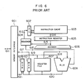
- Fig. 6 shows the general construction of the RISC-type computer. There are shown a memory interface 601, a program counter 602, an instruction cache 603, a sequencer 604, an instruction register 605, a decoder 606, a register file 607, an ALU 608, an MDR 609, and an MAR 610.
- Fig. 7 shows the process flow for the basic instructions.
- the instruction pointed by the program counter 602 is read by the instruction cache and set in the instruction register 605.
- the sequencer 604 controls the program counter 602 in response to an instruction signal 615 and a flag signal 616 from the ALU 608.
- the contents of the instruction pointer register is transferred through buses 618, 619 to the ALU 608.
- the ALU 608 makes arithmetic operation.
- the calculated result is stored in the registor file 607 through a bus 620.
- the instruction is limited only to the basic instruction.
- the arithmetic operation is made only between the registors, and the instruction including operand fetch is limited to the load instruction and the store instruction.
- the complicated instruction can be realized by a combination of basic instructions. Without use of the microinstruction, the contents of the instruction registor 605 is decoded directly by the decoder 606 and used to control the ALU 608 and so on.
- Fig. 7 shows the process flow for registor-registor arithmetic operation.
- the pipeline is formed of four stages since the instruction is simple.
- Fig. 8 shows the process flow for the time of conditional branch.
- the number of pipeline stages is small, and thus the waiting cycle is only one cycle.
- the loading of the operand from the memory can be performed in one machine cycle because of the presence of the address adder, while in the RISC-type computer shown in Fig. 6, the load instruction requires two machine cycles because it is decomposed into the address calculation instruction and the load instruction.
- the above objects can be achieved by providing a plurality of arithmetic operation units sharing the register file, simplifying the instructions to decrease the number of pipeline stages and reading a plurality of instructions in one machine cycle to control the plurality of arithmetic operation units.
- the complex instruction is decomposed into basic instructions, and a plurality of instructions are read at a time in one machine cycle and executed, so that the plurality of arithmetic operation units can be simultaneously operated thereby to enhance the processing ability.
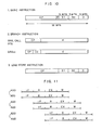
- Fig. 9 is the list of instructions to be executed by the processor of this embodiment.
- the basic instructions are all executed by the inter-register operation.
- the branch instructions include four branch instructions: an unconditional branch instruction BRA, a conditional branch instruction BRAcc (cc indicates the branch condition), a branch-to-subroutine instruction CALL, and a return-from-subroutine instruction RTN.
- a load instruction LOAD and a store instruction STORE are provided.
- the data format is only 32 bits whole number, it is not limited thereto.
- the address has 32 bits (4 bytes) for each instruction. For the sake of simplicity, the number of instructions are limited as above, but may be increased as long as the contents can be processed in one machine cycle.
- Fig. 10 shows the instruction format.
- the instructions all have a fixed length of 32 bits.
- the F, S1, S2, and D field of the basic instruction are, respectively, the bit or bits indicating whether the arithmetic operation result should be reflected on the flag, the field for indicating the first source register, the field for indicating the second source register, and the field for indicating the destination register.
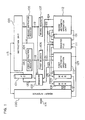
- Fig. 1 shows the construction of this embodiment. There are shown a memory interface 100, a 32-bit program counter 101, a sequencer 102, an instruction unit 103, a 32-bit first instruction register 104, a 32-bit second instruction register 105, a first decoder 106, a second decoder 107, an MDR 108, an MAR 109, a first arithmetic operation unit 110, a register file 111, and a second arithmetic operation unit 112.
- FIGs. 11 to 14 show the pipeline processing in this embodiment.
- the pipeline comprises four stages of the IF (Instruction Fetch), R (Read), EX (Execution), W (Write).
- the signal 116 fed from the instruction unit is the conflict signal indicative of various different conflicts between the first and second instructions.
- the conflict signal is asserted, the conflict is controlled to be avoided by the hardware. The method of avoiding conflicts will be described in detail later.
- the contents of the first instruction register 104 is decoded by the first decoder 106, and the contents of the second instruction register 105 is decoded by the second decoder 107.
- the contents of the register pointed by the first source register field S1 of the first instruction register 104 is fed to the first arithmetic operation unit 110 through a bus 125, and the contents of the register pointed by the second source register field S2 is fed through a bus 126 thereto.
- the contents of the register pointed by the first source register field S1 of the second instruction register is fed through a bus 127 to the second arithmetic operation unit 112, and the contents of the register pointed by the second source register field S2 is fed through a bus 128 thereto.
- the first arithmetic operation unit 110 makes an arithmetic operation for the data fed through the buses 125 and 126 in accordance with the contents of the OP code of the first instruction register.
- the second arithmetic operation unit 112 makes an arithmetic operation for the data fed through the buses 127 and 128 in accordance with the contents of the OP code of the second instruction register 105.
- the operation of the W stage will be mentioned below.
- the result of the arithmetic operation of the first arithmetic operation unit 110 is stored through a bus 129 in the register pointed by the destination field D of the first instruction register.
- the result of the arithmetic operation of the second operation unit 112 is stored through a bus 131 in the register pointed by the destination field D of the second instruction register.
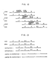
- Fig. 11 shows the flow chart for the continuous processing of basic instructions. Two instructions are processed at a time in one machine cycle. In this example, the first arithmetic operation unit and the second arithmetic operation unit are always operated in parallel.
- Fig. 12 is the flow chart for the continuous processing either load or store instruction as a first instruction, and the basic instruction as a second instruction.
- the load instruction is executed, at the R stage the contents of the register specified by the S2 field of the first instruction register is transferred through the bus 126 to the MAR 109.
- the operand is fetched through the memory interface 100.
- the operand fetched at the W stage is stored through the bus 129 in the register specified by the destination field D of the first instruction register.
- the operand can be fetched in one machine cycle if a high speed cache is provided in the memory interface. Particularly, it can be easily made if the whole computer shown in Fig. 1 is integrated in a semiconductor substrate with the instruction cache and data cache provided on the chip. Of course, when the cache is mis-hitted, the operand fetch cannot be finished in one machine cycle. In such case, the system clock is stopped, and the EX stage is extended. This operation is also performed in the conventional computer.
- the contents of the register pointed by the first source register field S1 of the first instruction register is transferred as data through the bus 125 to the MDR 108.
- the contents of the register pointed by the second source register field S2 of the first instruction register is transferred as address through the bus 126 to the MAR 109.
- the data within the MDR 108 is written in the address pointed by the MAR 109.
- Fig. 13 shows the process flow for the execution of the unconditional jump BRA instruction as the second instruction.
- the sequencer 102 makes the addition between the displacement field d and the program counter, and set it in the program counter 101.
- the instruction next to the address of the BRA instruction and the further next instruction are read (the instructions 1 and 2 shown in Fig. 13).
- two instructions at the addresses to which the program has been jumped are read.
- the hardware is able to execute the instructions 1 and 2. In other words, no waiting cycle occurs even at the time of processing the jump instruction. this approach is called the delay branch, and used in the conventional RISC-type computer.
- Fig. 14 shows the processing flow of the conditional branch instruction BRAcc.
- the flag is set by the instruction indicated by ADD, F, and the decision of whether the branch condition is met or not is made according to the result.
- the instruction next to the address of the BRAcc instruction, the instruction 1 in Fig. 14, the next instruction, and the instruction 2 in Fig. 14 are read and processed.
- the result of the arithmetic operation is weritten in the register file only when the branch condition of the BRAcc instruction is not satisfied. In other words, when the branch instruction is satisfied, the result of the computation is suppressed from being written.
- this embodiment processes two instructions at a time during one machine cycle, thus having the merit that the processing ability is enhanced to the double, maximum. Moreover, since simple instructions are used and the number of pipeline stages is as small as 4 under the control of the wired logic, the overhead at the time of branching can be reduced to one machine cycle, maximum. In addition, if the delay branch is optimized by the compiler, the overhead can be eliminated.
- the parallel operations of the first arithmetic operation unit 110 and the second arithmetic operation unit 112 in Fig. 1 can be performed with less idling as compared with that of the address adder and ALU by the parallel pipeline in the conventional CISC-type computer. This aspect will be mentioned a little more.
- the conventional CISC-type computer as shown in Fig. 15, is able to load a piece of data at a time during one machine cycle.
- this embodiment takes two instructions of the address computation ADD instruction and the LOAD instruction using the address for loading a piece of data, but is able to execute two instructions at a time during one machine cycle as shown in Fig. 16, thus still being able to load one piece of data at a time during one machine cycle. From the viewpoint of the parallel operation of arithmetic operation units, both operate two arithmetic operation units in parallel and thus are the same.
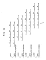
- Figs. 17 and 18 show the comparison of further complicated processings.
- the instruction 1 which, as shown in Fig. 17, takes 6-cycles processing at the EX stage in the conventional CISC-type computer can be executed in 3 cycles in this embodiment as shown in Fig. 18. This is because in the conventional CISC-type computer, the operation of the address adder is stopped during the execution of the instruction 1, while in this embodiment, two arithmetic operation units can be operated in parallel in each cycle.
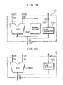
- Fig. 19 shows the construction of the first arithmetic operation unit 110 shown in Fig. 1.
- An ALU 1500 There are shown an ALU 1500, a barrel shifter 1501, and a flag generation circuit 1502.
- the data transferred through the buses 125 and 126 are processed by the ALU 1500 for the addition, subtraction, and logic operation and by the barrel shifter for the SFT instruction.
- the result of the processing is transmitted to the bus 130.
- a flag is produced from the flag generation circuit 1502 on the result of the arithmetic operation and fed as the signal 123.
- Fig. 20 shows one example of the construction of the second arithmetic operation unit 112 in Fig. 1.
- the second arithmetic operation unit is different from the first arithmetic operation unit in that it has no barrel shifter. This is because the SFT instruction occurs less frequently than the arithmetic logic oepration instruction. Thus, two SFT instructions cannot be executed in one machine cycle, but there is the merit that the amount of hardware can be reduced. The control method to be used when two SFT instructions appear will be described later.
- the second arithmetic unit 112 may be the unit shown in Fig. 19.
- Fig. 21 shows the construction of the register file 111 in Fig. 1.
- Each register has four read ports and two write ports.
- the bus switch is used to bypass the register file when the register specified by the destination field of the previous instruction is immediately used for the next instruction.
- the bus switch 1702 is the bypass switch from the bus 129 to the bus 127, and opens when the destination register field D of the first instruction coincides with the first source register field S1 of the second instruction.
- the above cases (1) and (2) in which the conflict occurs are the problems peculiar to this embodiment which are caused when the load, store instruction and the SFT instruction cannot be processed by the second arithmetic operation unit. If in Fig. 1 the second MDR is added to the bus 127, the second MAR is added to the bus 128, and two pieces of data are accessed to in one machine cycle through the memory interface, then the conflict condition (1) can be eliminated. Moreover, if the barrel shifter is provided in the second arithmetic operation unit, the conflict condition (2) can be elimianted. In this embodiment, the conflict condition occurs because of hardware reduction. In such case, since the conflict can be easily eliminated as described later, only the hardware associated with the instructions to be executed at a time is doubled in accordance with the necessary performance and the allowable amount of hardware and thus the hardware is reduced with substantially no reduction of performance.
- Fig. 22 shows the case where the SFT instruction is located in the address "3" for the second instruction.
- the lower part of Fig. 22 shows the instructions to be stored in the first and second instruction registers at the time of excution.
- the program counter is 2
- the hardware detects that the second instruction is the SFT instruction, and the instruction at the address 2 is set in the first instruction register, the NOP instruction being set in the second instruction register.
- the program counter is incremented by "1", or address 3 is set in the program counter.
- the SFT instruction at the address 3 is set in the first instruction register, and the NOP instruction in the second instruction register.
- the processing can be correctly made in two separate machine cycles.
- optimization is made by the compiler so that if possible, the SFT instruction is preferably prevented from appearing.
- Fig. 24 shows the processing method to be used when the load instruction appears as the second instruction.
- the load instruction is stored in the address 3.
- the processing method is the same as for the SFT instruction.
- Fig. 25 shows the processing method to be used when the register conflict occurs.
- the instruction at the address 2 is stored in the number-8 register, and the instruction at the address 3 reads the same number-8 register. In this case, it is executed in two separate machine cycles as is the SFT instruction.
- Fig. 26 shows the construction of the instruction unit 103 in Fig. 1.
- a conflict detection circuit 2300 There are shown a conflict detection circuit 2300, a cache memory 2301, a first mask circuit 2302, and a second mask circuit 2303.
- the contents of the program counter is, normally, inputted through the bus 113, and the instruction pointed by the program counter and the instruction at the next address are fed to buses 2305 and 2306.
- the instruction is fetched through the memory interface 100, and written through the bus 113 in the cache 2301.
- the conflict detection circuit checks if the conflict is present between the first and second instructions.
- the conflict signal 2304 is asserted.
- the cache are provided bits each indicating the conflict condition of two instructions.
- the conflict signal 2304 is stored therein.
- the first mask circuit receives the first instruction, the second instruction, the conflict bit, and the least significant bit of the program counter, and controls the signal 115 to the first instruction register 104 as shown in Fig. 27.
- the second mask circuit receives the second instruction, the conflict bit and the least significant bit of the program counter, and still supplies the signal 117 to the second register 105 as shown in Fig. 27.
- the conflict bit and the least significant bit of the PC are both 0, the first instruction is fed to the first instruction register, and the second instruction to the second instruction register.
- This operation is in the normal case.
- the conflict bit is 1, and the least significant bit of the PC is 0, the first instruction is fed to the first instruction register, and the NOP instruction to the second instruction register.
- This operation is the processing in the first machine cycle at the time of processing the conflict instruction.
- the conflict bit is 1, and the least significant bit of the PC is 1
- the second instruction is fed to the first instruction register, and the NOP instruction to the second instruction register.
- This operation is the processing in the second machine cycle at the time of processing the conflict instruction.
- Fig. 28 shows the construction of the instruction cache 2301 in Fig. 26.
- a directory 2500 There are shown a directory 2500, a data memory 2501, a selector 2502, an address register 2503, a write register 2504, a comparator 2505, and a cache control circuit 2506.
- the cache in Fig. 28 has substantially the same construction as the normal cache, but it is different in that the data memory 2501 has provided therein a conflict bit holding field for each 2-instruction 8 bytes, and that at the time of reading the cache, the least significant bit (0 bit) of the PC is neglected so that the first instruction 2305, the second instruction 2306 and the conflict signal 116 are fed.
- the data memory is of 8 K words, and the block size is 32 bytes (8 words).
- the signal 113 fed from the program counter is set in the address register 2503.
- the outputs of the directory 2500 and data memory 2501 are indicated by 3 to 12 bits of the address.
- the comparator 2505 compares the output of the directory and the bits 13 to 31 of the address register. If the result of the comparison is not coincident, a signal 2508 is supplied to the cache control circuit 2506.
- the cache control circuit 2506 reads a block including an instruction mis-hit from the main memory, and sets it in the data memory 2501.
- the selector 2502 receives the first and second bits of the address register, and selects two necessary instructions from the block. The first and second instructions are sure to be within the same block, and only one of them is never mis-hitted.
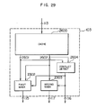
- Fig. 29 shows another construction of the instruction unit 103 in Fig. 1.
- a cache memory 2600 There are shown a conflict detection circuit 2604, a first mask circuit 2302, and a second mask circuit 2303.
- the construction shown in Fig. 29 is different from that shown in Fig. 26 in that the cache has no field for holding the conflict bit and that the first instruction 2601 and the second instruction 2602 of the cache output are monitored by the cycle conflict detection circuit 2604.
- the operations of the first mask circuit 2302 and the second mask circuit 2303 is the same as those in Fig. 26.
- the each-cycle conflict detection circuit is operated after reading the cache, the machine cycle is extented, but the Vietnamese bit field may be absent within the cache.
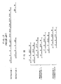
- conditional branch instruction by making effective use of the fact that two instructions are processed at a time in one machine cycle, it is possible to more fast process the conditional branch instruction in a special case. That is, when in the conditional branch instruction, the destination of the branching when the condition is satisfied is the next, and next instruction (instruction 2 in Fig. 30), the instructions 2 and 3 are executed irrespective of whether the condition is satisfied or not, and whether the W stage of the instruction 1 is suppressed or not is controlled by the satisfaction or not of the condition, so that when the condition is met, the waiting cyle can be eliminated. In this case, however, the conditional branch instruction is sure to be provided on the first instruction side.
- one waiting cycle occurs when the condition is satisfied, as described with reference to Fig. 14.
- the execution of instructions on the second instruction side can be controlled by whether the condition of the conditional branch instruction on the first instruction side is satisfied or not, without no effect on the instruction process flow of two-instruction units.
- Fig. 31A shows the processing in the conventional computer
- Fig. 31B shows that in this embodiment.
- Fig. 31A there is a possibility that an interruption enters between the instructions, while in Fig. 31B no interruption occurs between the instructions 1 and 2, and between the instructions 3 and 4.
- a program for other processes may enter between arbitrary instructions
- Fig. 31B there is the merit that the instructions 1 and 2 or the instructions 3 and 4 are sure to be executed in a sequence.
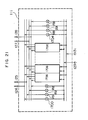
- Fig. 32 shows the construction of another embodiment of this invention.
- 4 instructions can be processed in one machine cycle at a time.
- a memory interface 3200 There are shown a memory interface 3200, a program counter 3201, a sequencer 3202, an instruction unit 3203, first to fourth instruction registers 3204 to 3207, first to fourth decoders 3208 to 3211, an MDR 3212, an MAR 3213, first to fourth arithmetic operation units 3214, 3215, 3217 and 3218, and a register file 3216.
- Each arithmetic operation unit shares the register file 3216. The operation of each portion is the same as in the embodiment shown in Fig. 1, and thus will not be described.
- the degree of parallel can be further increased, but since there is a program in which one branch instruction is present in each several intructions, extrme increase of the degree of parallel in such program will not be much effective. It is preferable to process about 2 to 4 instructions at a time. If the degree of parallel is further increased in the program with a few branches and a few conflicts, the performance is effectively increased. Moreover, if the degree of parallel is selected to be 2 n (n is a natural number), the instruction unit can easily be controlled.
- Fig. 33 shows three examples.
- the first instruction is stored in a main memory
- the second instruction is stored only on the head portion of the address space and stored in an ROM.
- the first and second instructions are stored in the head portion of the address space and stored in an ROM, and in the other portions of the main memory is stored only the first instruction.
- Fig. 33c which is substantially the same as that of Fig.
- the second instruction to be stored in an ROM is written in the intermediate portion of the address space.
- the whole construction of the computer is the same as in Fig. 1, and only the instruction unit 103 is required to be changed.
- the ROM portion is written a program with a high frequency of usage and with a high degree of parallel, which program is executed by a subroutine call from a routine. Since the ROM portion may be of a low capacity, a most suitable program can be produced by an assembler even without any compiler.
- Fig. 34 shows the construction of the instruction unit 103 in Fig. 1 which construction is for realizing the example of Fig. 33a.
- a cache 2900 There are shown a cache 2900, a 4 K words ROM 2901, a mask circuit 2903, and a mask circuit control circuit 2902.
- the mask circuit control circuit always monitors the address 113. Only when the more significant bits 12 to 31 of the address are all zero, an effective signal 2904 is asserted.
- the mask circuit 2903 only when the effective signal 2904 is asserted, supplies a ROM output 2905 to the second register as an output 117. In the other time, the NOP instruction is fed.
- the mask circuit control circuit 2902 shown in Fig. 34 is required to be constructed as shown in Fig. 35.
- a comparator 3000 and a base register 3001.
- the comparator 3000 asserts the effective signal 2904.
- the instruction unit 103 shown in Fig. 1 is required to be constructed as shown in Fig. 36.
- the functions of the ROM 2901, mask circuit control circuit 2902, and mask circuit 2903 are the same as those represented by the same numbers in Fig. 29.
- Fig. 36 there are shown a cache 3100, a 4 K word ROM 3101, a selector control circuit 3102, and a selector 3107.
- the selector control circuit 3102 always monitors the more significant bits 12 to 31 of the address 113. Only when all the bits are 0, an ROM selection signal 3105 is asserted.
- the selector 3107 only when the ROM selection circuit 3105 is asserted, supplies an ROM output signal 3104 to the first instruction register as the output 115. In the other time, the cache output 3103 is supplied.
- the hardware can be reduced by simultaneously processing a plurality of instructions for some portion, and forming that portion as an ROM. Also, since only for the ROM portion, most suitable design can be achieved by assembler, there is the merit that it is not necessary to develop the compiler considering the simultaneous processing of a plurality of instructions. Moreover, by rewriting the ROM portion, it is possible to realize the high speed operation for each application and suitable for each application.
- a complicated instruction is decomposed into basic instructions, and a plurality of instructions are read and executed at a time in one machine cycle, a plurality of arithmetic operation units can be operated at a time, and thus increase the processing ability.
Abstract
Description
- This invention relates to CPUs such as in minicomputers or microcomputers, and particularly to a data processor suitable for use in high speed operation.
- Hitherto, various means have been devised for the high speed operation of computers. The typical one is a pipeline system. The pipeline system does not complete the processing of one instruction before the next instruction is started to execute, but makes the execution of instructions in such a bucket-relay manner that when the execution of one instruction which is divided into a plurality of stages is going to enter into the second stage, the first stage of the next instruction which is similarly divided into a plurality of stages is started to execute. This system is described in detail in the book "ON THE PARALLEL COMPUTER STRUCTURE", written by Shingi Tomita, published by Shokodo, pages 25 to 68. By use of the n-stage pipeline system, it is possible to execute n instructions along all stages at a time and complete the processing of one instruction at each pipeline pitch though one instruction is processed at each pipeline stage.
- It is well known that the instruction architecture of a computer has a large effect on the processing method and the process performance. From the instruction architecture point of view, the computer can be grouped into the CISC (Complex Instruction Set Computer) and the RISC (Reduced Instruction Set Computer). The CISC processes complicated instructions by use of microinstructions, while the RISC treats simple instructions, and instead makes high speed computation using the hard wired logic control without use of microinstructions. Now, we will describe the summary of the hardware and the pipeline operation of both the conventional CISC and RISC.
- Fig. 2 shows the general construction of the CISC-type computer. There are shown a
memory interface 200, a program counter (PC) 201, aninstruction cache 202, aninstruction register 203, aninstruction decoder 204, an addresscalculation control circuit 205, a control storage (CS) 206 in which microinstructions are stored, a microprogram counter (MPC) 207, amicroinstruction register 208, adecoder 209, a register MDR (Memory Data Register) 210 which exchanges data with the memory, a register MAR (Memory Address Register) 211 which indicates the operand address in the memory, anaddress adder 212, aregister file 213, and an ALU (Arithmetic Logical Unit) 214. - The operation of the construction will be mentioned briefly. The instruction indicated by the PC 201 is taken out by the instruction cache and supplied through a
signal 217 to theinstruction register 203 where it is set. Theinstruction decoder 204 receives the instruction through asignal 218 and sets the head address of the microinstruction through asignal 220 in themicroiprogram counter 207. The addresscalculation control circuit 205 is ordered through asignal 219 to process the way to calculate the address. The addresscalculation control circuit 205 reads the register necessary for the address calculation, and controls theaddress adder 212. The contents of the register necessary for the address calculation is supplied from theregister file 213 throughbuses addres adder 212. On the other hand, the microinstruction is read from the CS 206 at every machine cycles, and decoded by thedecoder 209 and used to control theALU 214 and theregister file 213. In this case, acontrol signal 224 is supplied thereto. The ALU 214 calculates data fed from the register throughbuses register file 213 through abus 230. Thememory interface 200 is the circuit for exchanging with the memory such as fetching of instructions and operands. - The pipeline operation of the computer shown in Fig. 2 will be described with reference to Figs. 3, 4 and 5. The pipeline is formed of six stages. At the IF (Instruction Fetch) stage, an instruction is read by the
instruction cache 202 and set in theinstruction register 203. At the D (Decode) stage, theinstruction decoder 204 performs decoding of the instruction. At A (Address) stage, theaddress adder 212 carries out the calculation of the address of the operand. At the OF (Operand Fetch) stage, the operand of the address pointed by the MAR 211 is fetched through thememory interface 200 and set in the MDR 210. At the EX (Execution) stage, data is read by theregister file 213 and theMDR 210, and fed to theALU 214 where it is calculated. At the last W (Write) stage, the calculation result is stored through thebus 230 in one register of theregister file 213. - Fig. 3 shows the continuous processing of add instruction ADDs as one basic instruction. At each machine cycle, one instruction is processed, and the
ALU 214 andaddress adder 212 operate in parallel. - Fig. 4 shows the processing of the conditional branch instruction BRAcc. A flag is produced by the TEST instruction. Fig. 4 shows the flow at the time when the condition is met. Since the flag is produced at the EX stage, three-cycles waiting is necessary until the jumped-to-instruction is fetched, the more the number of stages is increased, the waiting cycle count is increased the more, resulting in the neck in the performance enhancement.
- Fig. 5 shows the execution flow of a complicated instruction. The
instruction 1 is the complicated instruction. The complicated instruction requires a great number of memory accesses as is the string copy and is normally processed by extending the EX stage many times. The EX stage is controlled by the microprogram. The microprogram is accessed to once per machine cycle. In other words, the complicated instruction is processed by reading the microprogram a plurality of times. At this time, since one instruction is processed at the EX stage, the next instruction (theinstruction 2 shown in Fig. 5) is required to wait. In such case, the ALU 214 operates at all times, and the address adder 212 idles. - The RISC-type computer will hereinafter be described. Fig. 6 shows the general construction of the RISC-type computer. There are shown a
memory interface 601, aprogram counter 602, aninstruction cache 603, a sequencer 604, aninstruction register 605, adecoder 606, aregister file 607, an ALU 608, an MDR 609, and anMAR 610. - Fig. 7 shows the process flow for the basic instructions. At the IF (Instruction Fetch) stage, the instruction pointed by the
program counter 602 is read by the instruction cache and set in theinstruction register 605. The sequencer 604 controls theprogram counter 602 in response to aninstruction signal 615 and aflag signal 616 from the ALU 608. At the R (Read) stage, the contents of the instruction pointer register is transferred throughbuses registor file 607 through abus 620. - In the RISC-type computer, the instruction is limited only to the basic instruction. The arithmetic operation is made only between the registors, and the instruction including operand fetch is limited to the load instruction and the store instruction. The complicated instruction can be realized by a combination of basic instructions. Without use of the microinstruction, the contents of the
instruction registor 605 is decoded directly by thedecoder 606 and used to control the ALU 608 and so on. - Fig. 7 shows the process flow for registor-registor arithmetic operation. The pipeline is formed of four stages since the instruction is simple.
- Fig. 8 shows the process flow for the time of conditional branch. As compared with the CISC-type computer, the number of pipeline stages is small, and thus the waiting cycle is only one cycle. In this case, in addition to the inter-register operation, it is necessary to load the operand from the memory and store the operand in the memory. In the CISC-type computer, the loading of the operand from the memory can be performed in one machine cycle because of the presence of the address adder, while in the RISC-type computer shown in Fig. 6, the load instruction requires two machine cycles because it is decomposed into the address calculation instruction and the load instruction.
- The problems with the above-mentioned prior art will be described briefly. In the CISC-type computer, although the memory-register instruction can be executed in one machine cycle because of the presence of the address adder, the overhead at the time of branching is large because of large number of pipeline stages. Moreover, only the E stage is repeated when a complicated instruction is executed, and as a result the address adder idles.
- In he RISC-type computer, the overhead at the time of branching is small because of small number of pipeline stages. However, for the memory-register operation without use of the address adder, two instructions are required of the load instruction and the inter-register operation instruction.
- Accordingly, it is a first object of this invention to provide a data processor capable of making effective use of a plurality of arithmetic operation units to enhance the processing ability.
- It is a second object of this invention to provide a data processor capable of reducing the overhead at the time of branching.
- It is a third object of this invention to provide a data processor capable of reducing the processing time for a complicated instruction for the memory-register oepration.
- The above objects can be achieved by providing a plurality of arithmetic operation units sharing the register file, simplifying the instructions to decrease the number of pipeline stages and reading a plurality of instructions in one machine cycle to control the plurality of arithmetic operation units.
- According to the preferred embodiments of this invention, the complex instruction is decomposed into basic instructions, and a plurality of instructions are read at a time in one machine cycle and executed, so that the plurality of arithmetic operation units can be simultaneously operated thereby to enhance the processing ability.
- Moreover, since the function of the instruction is simple, and since the number of pipeline stages can be decreased, the overhead at the time of branching can be reduced.
- Furthermore, since the plurality of arithmetic operation units are operated in parallel, the processing time for the complicated instruction can be reduced.
-
- Fig. 1 is a block diagram of the whole construction of one embodiment of this invention.
- Fig. 2 is a block digram of the whole construction of a conventional example.
- Figs. 3 to 5 are timing charts for the operation thereof.
- Fig. 6 is a block diagram of the whole construction of another conventional example.
- Figs. 7 and 8 are timing charts for the operation thereof.
- Fig. 9 shows the list of instructions to be used in one embodiment of this invention.
- Fig. 10 shows the format of the instruction associated with the embodiment of this invention.
- Figs. 11 to 14 are timing charts for the operation of the embodiment of this invention.
- Fig. 15 is a timing chart for the operation of the conventional example.
- Figs. 16 to 18 are timing charts for the operation of the embodiment of this invention.
- Fig. 19 is a construction diagram of the first
arithmetic operation unit 110 in Fig. 1. - Fig. 20 is a construction diagram of the
second arithmetric unit 112 in Fig. 1. - Fig. 21 is a construction diagram of the register file 111 in Fig. 1.
- Figs. 22 to 25 are diagrams useful for explaining the embodiment of this invention shown in Fig. 1.
- Fig. 26 is a construction diagram of the
instruction unit 103 in Fig. 1. - Fig. 27 is a diagram useful for explaining the operation thereof.
- Fig. 28 is a construction diagram of the
cache 2301 in Fig. 26. - Fig. 29 is another construction diagram of the
instruction unit 103 in Fig. 1. - Fig. 30 is a timing chart for the operation of the embodiment of this invention.
- Figs. 31A and 31B show the instruction formats.
- Fig. 32 is a block diagram of the whole construction of another embodiment of this invention.
- Figs. 33 to 36 are diagrams of other embodiments of this invention, which make simultaneous partial processing of a plurality of instructions.
- One embodiment of this invention will be described.
- Fig. 9 is the list of instructions to be executed by the processor of this embodiment. The basic instructions are all executed by the inter-register operation. The branch instructions include four branch instructions: an unconditional branch instruction BRA, a conditional branch instruction BRAcc (cc indicates the branch condition), a branch-to-subroutine instruction CALL, and a return-from-subroutine instruction RTN. In addition to these instructions, a load instruction LOAD and a store instruction STORE are provided. although, for convenience of explanation, the data format is only 32 bits whole number, it is not limited thereto. The address has 32 bits (4 bytes) for each instruction. For the sake of simplicity, the number of instructions are limited as above, but may be increased as long as the contents can be processed in one machine cycle.
- Fig. 10 shows the instruction format. The instructions all have a fixed length of 32 bits. The F, S1, S2, and D field of the basic instruction are, respectively, the bit or bits indicating whether the arithmetic operation result should be reflected on the flag, the field for indicating the first source register, the field for indicating the second source register, and the field for indicating the destination register.
- Fig. 1 shows the construction of this embodiment. There are shown a
memory interface 100, a 32-bit program counter 101, asequencer 102, aninstruction unit 103, a 32-bitfirst instruction register 104, a 32-bitsecond instruction register 105, afirst decoder 106, asecond decoder 107, an MDR 108, an MAR 109, a firstarithmetic operation unit 110, a register file 111, and a secondarithmetic operation unit 112. - In this emodiment, two instructions are read and executed in parallel in one machine cycle. Figs. 11 to 14 show the pipeline processing in this embodiment. The pipeline comprises four stages of the IF (Instruction Fetch), R (Read), EX (Execution), W (Write).
- The operation of this embodiment will be described with reference to Fig. 1.
- At the IF stage, two instructions pointed by the program counter are read, and set in the first and second instruction registers 104 and 105 through
buses sequencer 102 is the circuit for controlling the program counter. When the first and second instruction registers both indicate no branch instruction, the program counter is incremented to theprevious count + 2. At the time of branching, the branch address is computed and set in the program counter. When the conditional branch occurs, decision is made of whether the branch should be made or not on the basis of the flag information, 123 from the first arithmetic operation unit and the flag information, 124 from the second arithmetic operation unit. Thesignal 116 fed from the instruction unit is the conflict signal indicative of various different conflicts between the first and second instructions. When the conflict signal is asserted, the conflict is controlled to be avoided by the hardware. The method of avoiding conflicts will be described in detail later. - The operation of the R stage at the time of processing the basic instruction will be mentioned below. At the R stage, the contents of the
first instruction register 104 is decoded by thefirst decoder 106, and the contents of thesecond instruction register 105 is decoded by thesecond decoder 107. As a result, the contents of the register pointed by the first source register field S1 of thefirst instruction register 104 is fed to the firstarithmetic operation unit 110 through abus 125, and the contents of the register pointed by the second source register field S2 is fed through abus 126 thereto. Moreover, the contents of the register pointed by the first source register field S1 of the second instruction register is fed through abus 127 to the secondarithmetic operation unit 112, and the contents of the register pointed by the second source register field S2 is fed through abus 128 thereto. - The operation of the EX stage will hereinafter be described. At the EX stage, the first
arithmetic operation unit 110 makes an arithmetic operation for the data fed through thebuses arithmetic operation unit 112 makes an arithmetic operation for the data fed through thebuses second instruction register 105. - Finally, the operation of the W stage will be mentioned below. At the W stage, the result of the arithmetic operation of the first
arithmetic operation unit 110 is stored through abus 129 in the register pointed by the destination field D of the first instruction register. Also, the result of the arithmetic operation of thesecond operation unit 112 is stored through abus 131 in the register pointed by the destination field D of the second instruction register. - Fig. 11 shows the flow chart for the continuous processing of basic instructions. Two instructions are processed at a time in one machine cycle. In this example, the first arithmetic operation unit and the second arithmetic operation unit are always operated in parallel.
- Fig. 12 is the flow chart for the continuous processing either load or store instruction as a first instruction, and the basic instruction as a second instruction. When the load instruction is executed, at the R stage the contents of the register specified by the S2 field of the first instruction register is transferred through the
bus 126 to the MAR 109. At the EX stage, the operand is fetched through thememory interface 100. Finally, the operand fetched at the W stage is stored through thebus 129 in the register specified by the destination field D of the first instruction register. - At the EX stage, the operand can be fetched in one machine cycle if a high speed cache is provided in the memory interface. Particularly, it can be easily made if the whole computer shown in Fig. 1 is integrated in a semiconductor substrate with the instruction cache and data cache provided on the chip. Of course, when the cache is mis-hitted, the operand fetch cannot be finished in one machine cycle. In such case, the system clock is stopped, and the EX stage is extended. This operation is also performed in the conventional computer.
- When the store instruction is executed, at the R state the contents of the register pointed by the first source register field S1 of the first instruction register is transferred as data through the
bus 125 to the MDR 108. At the same time, the contents of the register pointed by the second source register field S2 of the first instruction register is transferred as address through thebus 126 to the MAR 109. At the EX stage, the data within the MDR 108 is written in the address pointed by the MAR 109. - As shown in Fig. 12, even if the load instruction or the store instruction is the first instruction, two instructions can be processed at a time in one machine cycle. The case where the load instruction or the store instruction appears as the second instruction will be mentioned in detail later.
- Fig. 13 shows the process flow for the execution of the unconditional jump BRA instruction as the second instruction. When the BRA instruction is read, at the R stage the
sequencer 102 makes the addition between the displacement field d and the program counter, and set it in theprogram counter 101. During this time, the instruction next to the address of the BRA instruction and the further next instruction are read (theinstructions instructions instructions - Fig. 14 shows the processing flow of the conditional branch instruction BRAcc. The flag is set by the instruction indicated by ADD, F, and the decision of whether the branch condition is met or not is made according to the result. At this time, similarly as at the time of the unconditional branch instruction processing mentioned with reference to Fig. 13, the instruction next to the address of the BRAcc instruction, the
instruction 1 in Fig. 14, the next instruction, and theinstruction 2 in Fig. 14 are read and processed. However, at the W stage during the processing flow of the two instructions, the result of the arithmetic operation is weritten in the register file only when the branch condition of the BRAcc instruction is not satisfied. In other words, when the branch instruction is satisfied, the result of the computation is suppressed from being written. - Thus, as shown in Figs. 11 to 14, this embodiment processes two instructions at a time during one machine cycle, thus having the merit that the processing ability is enhanced to the double, maximum. Moreover, since simple instructions are used and the number of pipeline stages is as small as 4 under the control of the wired logic, the overhead at the time of branching can be reduced to one machine cycle, maximum. In addition, if the delay branch is optimized by the compiler, the overhead can be eliminated.
- Moreover, since even complicated processings can be executed by a combination of simple instructions, the parallel operations of the first
arithmetic operation unit 110 and the secondarithmetic operation unit 112 in Fig. 1 can be performed with less idling as compared with that of the address adder and ALU by the parallel pipeline in the conventional CISC-type computer. This aspect will be mentioned a little more. When the load from the memory to the register is repeated, the conventional CISC-type computer, as shown in Fig. 15, is able to load a piece of data at a time during one machine cycle. On the contrary, this embodiment takes two instructions of the address computation ADD instruction and the LOAD instruction using the address for loading a piece of data, but is able to execute two instructions at a time during one machine cycle as shown in Fig. 16, thus still being able to load one piece of data at a time during one machine cycle. From the viewpoint of the parallel operation of arithmetic operation units, both operate two arithmetic operation units in parallel and thus are the same. - Figs. 17 and 18 show the comparison of further complicated processings. The
instruction 1 which, as shown in Fig. 17, takes 6-cycles processing at the EX stage in the conventional CISC-type computer can be executed in 3 cycles in this embodiment as shown in Fig. 18. This is because in the conventional CISC-type computer, the operation of the address adder is stopped during the execution of theinstruction 1, while in this embodiment, two arithmetic operation units can be operated in parallel in each cycle. - Fig. 19 shows the construction of the first
arithmetic operation unit 110 shown in Fig. 1. There are shown anALU 1500, abarrel shifter 1501, and aflag generation circuit 1502. The data transferred through thebuses ALU 1500 for the addition, subtraction, and logic operation and by the barrel shifter for the SFT instruction. The result of the processing is transmitted to thebus 130. A flag is produced from theflag generation circuit 1502 on the result of the arithmetic operation and fed as thesignal 123. - Fig. 20 shows one example of the construction of the second
arithmetic operation unit 112 in Fig. 1. There are shown anALU 1600, and aflag generation circuit 1601. The second arithmetic operation unit is different from the first arithmetic operation unit in that it has no barrel shifter. This is because the SFT instruction occurs less frequently than the arithmetic logic oepration instruction. Thus, two SFT instructions cannot be executed in one machine cycle, but there is the merit that the amount of hardware can be reduced. The control method to be used when two SFT instructions appear will be described later. Of course, the secondarithmetic unit 112 may be the unit shown in Fig. 19. - Fig. 21 shows the construction of the register file 111 in Fig. 1. There are shown
registers 1708, andbus switches 1700 to 1709. Each register has four read ports and two write ports. The bus switch is used to bypass the register file when the register specified by the destination field of the previous instruction is immediately used for the next instruction. For example, thebus switch 1702 is the bypass switch from thebus 129 to thebus 127, and opens when the destination register field D of the first instruction coincides with the first source register field S1 of the second instruction. - The method of eliminating the conflict between the first and second instructions will be described with reference to figs. 22 to 29. Both instructions cannot sometimes be executed at a time depending on a combination of the first and second instructions. This is called the conflict. The conflict occurs in the following cases.
- (1) Load or store instruction appears as the second instruction.
- (2) SFT instruction appears as the second instruction.
- (3) The register pointed by the destination register field D of the first instruction coincides with the register specified by the first source register field S1 of the second instruction or with the register pointed by the second source register field S2 of the second instruction.
- The above cases (1) and (2) in which the conflict occurs are the problems peculiar to this embodiment which are caused when the load, store instruction and the SFT instruction cannot be processed by the second arithmetic operation unit. If in Fig. 1 the second MDR is added to the
bus 127, the second MAR is added to thebus 128, and two pieces of data are accessed to in one machine cycle through the memory interface, then the conflict condition (1) can be eliminated. Moreover, if the barrel shifter is provided in the second arithmetic operation unit, the conflict condition (2) can be elimianted. In this embodiment, the conflict condition occurs because of hardware reduction. In such case, since the conflict can be easily eliminated as described later, only the hardware associated with the instructions to be executed at a time is doubled in accordance with the necessary performance and the allowable amount of hardware and thus the hardware is reduced with substantially no reduction of performance. - The control method to be used when the SFT instruction appears as the second instruction will be mentioned with reference to Fig. 22.
- The upper part of Fig. 22 shows the case where the SFT instruction is located in the address "3" for the second instruction. The lower part of Fig. 22 shows the instructions to be stored in the first and second instruction registers at the time of excution. When the program counter is 2, the hardware detects that the second instruction is the SFT instruction, and the instruction at the
address 2 is set in the first instruction register, the NOP instruction being set in the second instruction register. In the next machine cycle, the program counter is incremented by "1", oraddress 3 is set in the program counter. Moreover, the SFT instruction at theaddress 3 is set in the first instruction register, and the NOP instruction in the second instruction register. Thus, the processing can be correctly made in two separate machine cycles. Of course, optimization is made by the compiler so that if possible, the SFT instruction is preferably prevented from appearing. - Another method of eliminating the conflict will be described with reference to Fig. 23. The SFT instruction is prevented from being stored in the odd address for the second instruction, and when there is no instruction to be executed, the NOP instruction is stored therein. Thus, the program size is slightly increased, but the hardware for the elimination of the conflict can be omitted.
- Fig. 24 shows the processing method to be used when the load instruction appears as the second instruction. The load instruction is stored in the
address 3. The processing method is the same as for the SFT instruction. - Fig. 25 shows the processing method to be used when the register conflict occurs. The instruction at the
address 2 is stored in the number-8 register, and the instruction at theaddress 3 reads the same number-8 register. In this case, it is executed in two separate machine cycles as is the SFT instruction. - As to the load, store instruction and register conflict, too, it can be inhibited from being stored in the odd addresses for the purpose of eliminating the conflict. The effect is the same as described for the SFT instruction.
- A description will be made of the hardware system for realizing the processing system mentioned with reference to Figs. 22 to 25. Fig. 26 shows the construction of the
instruction unit 103 in Fig. 1. There are shown aconflict detection circuit 2300, acache memory 2301, afirst mask circuit 2302, and asecond mask circuit 2303. The contents of the program counter is, normally, inputted through thebus 113, and the instruction pointed by the program counter and the instruction at the next address are fed tobuses memory interface 100, and written through thebus 113 in thecache 2301. At this time, the conflict detection circuit checks if the conflict is present between the first and second instructions. If the conflict is present, theconflict signal 2304 is asserted. In the cache are provided bits each indicating the conflict condition of two instructions. At the time of cache mis-hitting, theconflict signal 2304 is stored therein. The first mask circuit receives the first instruction, the second instruction, the conflict bit, and the least significant bit of the program counter, and controls thesignal 115 to thefirst instruction register 104 as shown in Fig. 27. The second mask circuit receives the second instruction, the conflict bit and the least significant bit of the program counter, and still supplies thesignal 117 to thesecond register 105 as shown in Fig. 27. - When as shown in Fig. 27 the conflict bit and the least significant bit of the PC are both 0, the first instruction is fed to the first instruction register, and the second instruction to the second instruction register. This operation is in the normal case. When the conflict bit is 1, and the least significant bit of the PC is 0, the first instruction is fed to the first instruction register, and the NOP instruction to the second instruction register. This operation is the processing in the first machine cycle at the time of processing the conflict instruction. When the conflict bit is 1, and the least significant bit of the PC is 1, the second instruction is fed to the first instruction register, and the NOP instruction to the second instruction register. This operation is the processing in the second machine cycle at the time of processing the conflict instruction. Thus, the process flow of the conflict instruction mentioned with reference to Figs. 22, 23, and 25 can be realized by the processing.
- When the branch instruction is branched into an odd address, as shown in Fig. 27 only the second instruction is made effective irrespective of the conflict bit and thus correct processing is possible. The cache is read in each cycle, but it is written when the cache is mis-hitted, in which case it is made over several machine cycles. Thus, if the conflict detection circuit is operated at the time of writing the cache so that the conflict bit is ketp in the cache, the machine cycle can be effectively shorted.
- Fig. 28 shows the construction of the
instruction cache 2301 in Fig. 26. There are shown adirectory 2500, adata memory 2501, aselector 2502, anaddress register 2503, awrite register 2504, acomparator 2505, and acache control circuit 2506. The cache in Fig. 28 has substantially the same construction as the normal cache, but it is different in that thedata memory 2501 has provided therein a conflict bit holding field for each 2-instruction 8 bytes, and that at the time of reading the cache, the least significant bit (0 bit) of the PC is neglected so that thefirst instruction 2305, thesecond instruction 2306 and theconflict signal 116 are fed. - In Fig. 28, the data memory is of 8 K words, and the block size is 32 bytes (8 words). The
signal 113 fed from the program counter is set in theaddress register 2503. The outputs of thedirectory 2500 anddata memory 2501 are indicated by 3 to 12 bits of the address. Thecomparator 2505 compares the output of the directory and thebits 13 to 31 of the address register. If the result of the comparison is not coincident, asignal 2508 is supplied to thecache control circuit 2506. Thecache control circuit 2506 reads a block including an instruction mis-hit from the main memory, and sets it in thedata memory 2501. Theselector 2502 receives the first and second bits of the address register, and selects two necessary instructions from the block. The first and second instructions are sure to be within the same block, and only one of them is never mis-hitted. - Fig. 29 shows another construction of the
instruction unit 103 in Fig. 1. There are shown acache memory 2600, aconflict detection circuit 2604, afirst mask circuit 2302, and asecond mask circuit 2303. The construction shown in Fig. 29 is different from that shown in Fig. 26 in that the cache has no field for holding the conflict bit and that thefirst instruction 2601 and thesecond instruction 2602 of the cache output are monitored by the cycleconflict detection circuit 2604. The operations of thefirst mask circuit 2302 and thesecond mask circuit 2303 is the same as those in Fig. 26. According to this embodiment, since the each-cycle conflict detection circuit is operated after reading the cache, the machine cycle is extented, but the conflit bit field may be absent within the cache. - Moreover, according to this invention, by making effective use of the fact that two instructions are processed at a time in one machine cycle, it is possible to more fast process the conditional branch instruction in a special case. That is, when in the conditional branch instruction, the destination of the branching when the condition is satisfied is the next, and next instruction (
instruction 2 in Fig. 30), theinstructions instruction 1 is suppressed or not is controlled by the satisfaction or not of the condition, so that when the condition is met, the waiting cyle can be eliminated. In this case, however, the conditional branch instruction is sure to be provided on the first instruction side. In the normal conditional branching, one waiting cycle occurs when the condition is satisfied, as described with reference to Fig. 14. In other words, since in this invention, two instructions are processed in one machine cycle at a time, the execution of instructions on the second instruction side can be controlled by whether the condition of the conditional branch instruction on the first instruction side is satisfied or not, without no effect on the instruction process flow of two-instruction units. - Moreover, in this embodiment, by making effective use of the processing of two instructions in one machine cycle at a time, it is possible to realize the "atomic" processing with ease. The atomic processing is the processing which is always made in a sequence, and which is used for the synchronization between processes. Fig. 31A shows the processing in the conventional computer, and Fig. 31B shows that in this embodiment. In Fig. 31A, there is a possibility that an interruption enters between the instructions, while in Fig. 31B no interruption occurs between the
instructions instructions instructions instructions - Fig. 32 shows the construction of another embodiment of this invention. In this embodiment, 4 instructions can be processed in one machine cycle at a time. There are shown a
memory interface 3200, aprogram counter 3201, asequencer 3202, aninstruction unit 3203, first tofourth instruction registers 3204 to 3207, first tofourth decoders 3208 to 3211, anMDR 3212, anMAR 3213, first to fourtharithmetic operation units register file 3216. Each arithmetic operation unit shares theregister file 3216. The operation of each portion is the same as in the embodiment shown in Fig. 1, and thus will not be described. - Simialrly, the degree of parallel can be further increased, but since there is a program in which one branch instruction is present in each several intructions, extrme increase of the degree of parallel in such program will not be much effective. It is preferable to process about 2 to 4 instructions at a time. If the degree of parallel is further increased in the program with a few branches and a few conflicts, the performance is effectively increased. Moreover, if the degree of parallel is selected to be 2n (n is a natural number), the instruction unit can easily be controlled.
- Still another embodiment of this invention will be mentioned. In the above embodiments described so far, a plurality of instructions are always processed at a time. It is also possible to obtain a profit by normally processing one instruction in one machine cycle and at some case, processing a plurality of instructions at a time. Fig. 33 shows three examples. In the example of Fig. 33a, the first instruction is stored in a main memory, and the second instruction is stored only on the head portion of the address space and stored in an ROM. In the example of Fig. 33b, the first and second instructions are stored in the head portion of the address space and stored in an ROM, and in the other portions of the main memory is stored only the first instruction. In the example of Fig. 33c which is substantially the same as that of Fig. 33a, the second instruction to be stored in an ROM is written in the intermediate portion of the address space. The whole construction of the computer is the same as in Fig. 1, and only the
instruction unit 103 is required to be changed. In the ROM portion, is written a program with a high frequency of usage and with a high degree of parallel, which program is executed by a subroutine call from a routine. Since the ROM portion may be of a low capacity, a most suitable program can be produced by an assembler even without any compiler. - Fig. 34 shows the construction of the
instruction unit 103 in Fig. 1 which construction is for realizing the example of Fig. 33a. There are shown acache 2900, a 4K words ROM 2901, amask circuit 2903, and a maskcircuit control circuit 2902. The mask circuit control circuit always monitors theaddress 113. Only when the moresignificant bits 12 to 31 of the address are all zero, aneffective signal 2904 is asserted. Themask circuit 2903, only when theeffective signal 2904 is asserted, supplies aROM output 2905 to the second register as anoutput 117. In the other time, the NOP instruction is fed. - In order to realize the example of Fig. 33c, the mask
circuit control circuit 2902 shown in Fig. 34 is required to be constructed as shown in Fig. 35. There are shown acomparator 3000, and abase register 3001. When the moresignificant bits 12 to 31 of the base register are coincident with the moresignificant bits 12 to 31 of theaddress 113, thecomparator 3000 asserts theeffective signal 2904. - In order to realize the example of Fig. 33b, the
instruction unit 103 shown in Fig. 1 is required to be constructed as shown in Fig. 36. The functions of theROM 2901, maskcircuit control circuit 2902, andmask circuit 2903 are the same as those represented by the same numbers in Fig. 29. In Fig. 36, there are shown acache 3100, a 4K word ROM 3101, aselector control circuit 3102, and aselector 3107. Theselector control circuit 3102 always monitors the moresignificant bits 12 to 31 of theaddress 113. Only when all the bits are 0, anROM selection signal 3105 is asserted. Theselector 3107, only when theROM selection circuit 3105 is asserted, supplies anROM output signal 3104 to the first instruction register as theoutput 115. In the other time, thecache output 3103 is supplied. - As described with reference with Figs. 33 to 36, the hardware can be reduced by simultaneously processing a plurality of instructions for some portion, and forming that portion as an ROM. Also, since only for the ROM portion, most suitable design can be achieved by assembler, there is the merit that it is not necessary to develop the compiler considering the simultaneous processing of a plurality of instructions. Moreover, by rewriting the ROM portion, it is possible to realize the high speed operation for each application and suitable for each application.
- According to this invention, since a complicated instruction is decomposed into basic instructions, and a plurality of instructions are read and executed at a time in one machine cycle, a plurality of arithmetic operation units can be operated at a time, and thus increase the processing ability.
- Moreover, since the instructions have simple functions, and thus the number of pipeline stages can be decreased, the overhead upon branching can be made small.
- Furthermore, since a plurality of arithmetic operation units are operated in parallel, the processing time for a complicated process can be decreased.
Claims (15)
a program counter (101; 3201) for indicating an address of an instruction to be read;
m (m = 2, 3, ...) instruction registers (104, 105; 3204-3207) for storing at a time in one machine cycle a sequence of m instructions of which the first address is indicated by said program counter;
a register file (111; 3216) formed of a plurality of registers in which data are stored; and
m arithmetic operation units (110, 112; 3214, 3215, 3217, 3218) which read corresponding data from said register file and carry out parallelly arithmetic operations in accordance with instructions read from said instruction registers;
whereby the contents of said program counter is increased by m at a time, sequential m instructions are read from the addresses pointed by said program counter and written in said instruction registers, and said m instructions are processed in parallel by said m arithmetic operation units.
means (2300; 2604) for detecting whether one instruction of said m instructions has a conflict with a subsequent instruction or not; and
means for controlling to substantially execute only said one instruction in one machine cycle when said detection means detected said conflict.
a cache memory for instructions which is provided before said instruction registers;
wherein said detection means includes means (2300) for writing a conflict bit indicating said conflict at every m instructions which are read at a time, within said cache memory.
a cache memory for instructions which is provided before said instruction registers;
wherein said detection means includes means (2604) for monitoring at each machine cycle the conflict between instructions produced from said cache memory.
a program counter (101; 3201) for indicating the address of instructions to be read;
m (m = 2, 3, ...) instruction registers (104, 105; 3204-3207) for storing at a time in one machine cycle sequentially m instructions of which the first address is indicated by said program counter;
a register file (111; 3216) formed of a plurality of registers in which data is stored; and
m arithmetic operation units (110, 112; 3214, 3215, 3217, 3218) for reading corresponding data from said register file and making arithmetic operations in parallel in accordance with the instructions read from said instruction registers;
whereby only when the contents of said program counter is within a limited range, sequential m instructions of which the first address is indicated by said program counter are read and written in said instruction registers, said m instructions are processed by said m arithmetic operation units, and when the contents of said program counter is out of said range, ℓ (ℓ > m, ℓ = 1, 2, ...) instructions are read in said instruction registers and processed in parallel by ℓ arithmetic operation units.
Priority Applications (2)
| Application Number | Priority Date | Filing Date | Title |
|---|---|---|---|
| EP97103969A EP0782071B1 (en) | 1988-11-11 | 1989-11-10 | Data processor |
| EP99122100A EP0996057B1 (en) | 1988-11-11 | 1989-11-10 | Data processor with an instruction unit having a cache and a ROM |
Applications Claiming Priority (2)
| Application Number | Priority Date | Filing Date | Title |
|---|---|---|---|
| JP63283673A JP2810068B2 (en) | 1988-11-11 | 1988-11-11 | Processor system, computer system, and instruction processing method |
| JP283673/88 | 1988-11-11 |
Related Child Applications (2)
| Application Number | Title | Priority Date | Filing Date |
|---|---|---|---|
| EP97103969A Division EP0782071B1 (en) | 1988-11-11 | 1989-11-10 | Data processor |
| EP97103969.8 Division-Into | 1997-03-10 |
Publications (3)
| Publication Number | Publication Date |
|---|---|
| EP0368332A2 true EP0368332A2 (en) | 1990-05-16 |
| EP0368332A3 EP0368332A3 (en) | 1992-07-15 |
| EP0368332B1 EP0368332B1 (en) | 1997-09-24 |
Family
ID=17668583
Family Applications (3)
| Application Number | Title | Priority Date | Filing Date |
|---|---|---|---|
| EP97103969A Expired - Lifetime EP0782071B1 (en) | 1988-11-11 | 1989-11-10 | Data processor |
| EP89120881A Expired - Lifetime EP0368332B1 (en) | 1988-11-11 | 1989-11-10 | Pipeline data processor |
| EP99122100A Expired - Lifetime EP0996057B1 (en) | 1988-11-11 | 1989-11-10 | Data processor with an instruction unit having a cache and a ROM |
Family Applications Before (1)
| Application Number | Title | Priority Date | Filing Date |
|---|---|---|---|
| EP97103969A Expired - Lifetime EP0782071B1 (en) | 1988-11-11 | 1989-11-10 | Data processor |
Family Applications After (1)
| Application Number | Title | Priority Date | Filing Date |
|---|---|---|---|
| EP99122100A Expired - Lifetime EP0996057B1 (en) | 1988-11-11 | 1989-11-10 | Data processor with an instruction unit having a cache and a ROM |
Country Status (5)
| Country | Link |
|---|---|
| US (3) | US5233694A (en) |
| EP (3) | EP0782071B1 (en) |
| JP (1) | JP2810068B2 (en) |
| KR (2) | KR0149658B1 (en) |
| DE (3) | DE68928340T2 (en) |
Cited By (16)
| Publication number | Priority date | Publication date | Assignee | Title |
|---|---|---|---|---|
| EP0471191A2 (en) * | 1990-08-15 | 1992-02-19 | Hitachi, Ltd. | Data processor capable of simultaneous execution of two instructions |
| EP0488819A2 (en) * | 1990-11-30 | 1992-06-03 | Kabushiki Kaisha Toshiba | Conditional branch instructions execution apparatus |
| WO1993001546A1 (en) * | 1991-07-08 | 1993-01-21 | Seiko Epson Corporation | Extensible risc microprocessor architecture |
| WO1993001545A1 (en) * | 1991-07-08 | 1993-01-21 | Seiko Epson Corporation | High-performance risc microprocessor architecture |
| EP0525375A2 (en) * | 1991-06-24 | 1993-02-03 | Hitachi, Ltd. | Microcomputer and divider circuit |
| EP0528278A2 (en) * | 1991-08-13 | 1993-02-24 | Hitachi, Ltd. | Digital signal processor |
| FR2686717A1 (en) * | 1992-01-23 | 1993-07-30 | Intel Corp | MICROPROCESSOR HAVING A UNIT FOR EXECUTING PARALLEL INSTRUCTIONS. |
| US5367694A (en) * | 1990-08-31 | 1994-11-22 | Kabushiki Kaisha Toshiba | RISC processor having a cross-bar switch |
| US5416911A (en) * | 1993-02-02 | 1995-05-16 | International Business Machines Corporation | Performance enhancement for load multiple register instruction |
| US5448705A (en) * | 1991-07-08 | 1995-09-05 | Seiko Epson Corporation | RISC microprocessor architecture implementing fast trap and exception state |
| EP0919911A2 (en) * | 1997-11-26 | 1999-06-02 | Nec Corporation | Instruction execution cycle control circuit and control method for controlling execution cycle of instruction in pipeline processing |
| US5961629A (en) * | 1991-07-08 | 1999-10-05 | Seiko Epson Corporation | High performance, superscalar-based computer system with out-of-order instruction execution |
| US5983334A (en) * | 1992-03-31 | 1999-11-09 | Seiko Epson Corporation | Superscalar microprocessor for out-of-order and concurrently executing at least two RISC instructions translating from in-order CISC instructions |
| US6205535B1 (en) | 1991-06-24 | 2001-03-20 | Hitachi, Ltd. | Branch instruction having different field lengths for unconditional and conditional displacements |
| US7000097B2 (en) | 1992-09-29 | 2006-02-14 | Seiko Epson Corporation | System and method for handling load and/or store operations in a superscalar microprocessor |
| US7844797B2 (en) | 1992-09-29 | 2010-11-30 | Seiko Epson Corporation | System and method for handling load and/or store operations in a superscalar microprocessor |
Families Citing this family (84)
| Publication number | Priority date | Publication date | Assignee | Title |
|---|---|---|---|---|
| US5504932A (en) * | 1990-05-04 | 1996-04-02 | International Business Machines Corporation | System for executing scalar instructions in parallel based on control bits appended by compounding decoder |
| EP0459232B1 (en) * | 1990-05-29 | 1998-12-09 | National Semiconductor Corporation | Partially decoded instruction cache and method therefor |
| JP2532300B2 (en) * | 1990-10-17 | 1996-09-11 | 三菱電機株式会社 | Instruction supply device in parallel processing device |
| JP2682232B2 (en) * | 1990-11-21 | 1997-11-26 | 松下電器産業株式会社 | Floating point processor |
| RU1804645C (en) * | 1991-03-27 | 1993-03-23 | Институт Точной Механики И Вычислительной Техники Им.С.А.Лебедева | Central processor |
| US5488729A (en) * | 1991-05-15 | 1996-01-30 | Ross Technology, Inc. | Central processing unit architecture with symmetric instruction scheduling to achieve multiple instruction launch and execution |
| US5493687A (en) | 1991-07-08 | 1996-02-20 | Seiko Epson Corporation | RISC microprocessor architecture implementing multiple typed register sets |
| JP2875909B2 (en) * | 1991-07-12 | 1999-03-31 | 三菱電機株式会社 | Parallel processing unit |
| GB9123271D0 (en) * | 1991-11-02 | 1991-12-18 | Int Computers Ltd | Data processing system |
| EP0855647A1 (en) * | 1992-01-06 | 1998-07-29 | Hitachi, Ltd. | Computer for performing data fetch and data prefetch in parallel |
| DE4237417C2 (en) * | 1992-03-25 | 1997-01-30 | Hewlett Packard Co | Data processing system |
| DE69311330T2 (en) | 1992-03-31 | 1997-09-25 | Seiko Epson Corp | COMMAND SEQUENCE PLANNING FROM A RISC SUPER SCALAR PROCESSOR |
| US5371864A (en) * | 1992-04-09 | 1994-12-06 | International Business Machines Corporation | Apparatus for concurrent multiple instruction decode in variable length instruction set computer |
| WO1993022722A1 (en) | 1992-05-01 | 1993-11-11 | Seiko Epson Corporation | A system and method for retiring instructions in a superscalar microprocessor |
| US5416913A (en) * | 1992-07-27 | 1995-05-16 | Intel Corporation | Method and apparatus for dependency checking in a multi-pipelined microprocessor |
| JP3531166B2 (en) | 1992-12-31 | 2004-05-24 | セイコーエプソン株式会社 | Register renaming system and method |
| US5628021A (en) | 1992-12-31 | 1997-05-06 | Seiko Epson Corporation | System and method for assigning tags to control instruction processing in a superscalar processor |
| JP3182591B2 (en) * | 1993-01-20 | 2001-07-03 | 株式会社日立製作所 | Microprocessor |
| US5673409A (en) * | 1993-03-31 | 1997-09-30 | Vlsi Technology, Inc. | Self-defining instruction size |
| US5560025A (en) * | 1993-03-31 | 1996-09-24 | Intel Corporation | Entry allocation apparatus and method of same |
| US5463748A (en) * | 1993-06-30 | 1995-10-31 | Intel Corporation | Instruction buffer for aligning instruction sets using boundary detection |
| CA2123442A1 (en) * | 1993-09-20 | 1995-03-21 | David S. Ray | Multiple execution unit dispatch with instruction dependency |
| US5689672A (en) * | 1993-10-29 | 1997-11-18 | Advanced Micro Devices, Inc. | Pre-decoded instruction cache and method therefor particularly suitable for variable byte-length instructions |
| EP0651332B1 (en) * | 1993-10-29 | 2001-07-18 | Advanced Micro Devices, Inc. | Linearly addressable microprocessor cache |
| US5878245A (en) | 1993-10-29 | 1999-03-02 | Advanced Micro Devices, Inc. | High performance load/store functional unit and data cache |
| DE69434669T2 (en) * | 1993-10-29 | 2006-10-12 | Advanced Micro Devices, Inc., Sunnyvale | Speculative command queue for variable byte length commands |
| US5630082A (en) * | 1993-10-29 | 1997-05-13 | Advanced Micro Devices, Inc. | Apparatus and method for instruction queue scanning |
| DE69427265T2 (en) | 1993-10-29 | 2002-05-02 | Advanced Micro Devices Inc | Superskalarbefehlsdekoder |
| US5604909A (en) | 1993-12-15 | 1997-02-18 | Silicon Graphics Computer Systems, Inc. | Apparatus for processing instructions in a computing system |
| US5974534A (en) * | 1994-02-14 | 1999-10-26 | Hewlett-Packard Company | Predecoding and steering mechanism for instructions in a superscalar processor |
| US5537629A (en) * | 1994-03-01 | 1996-07-16 | Intel Corporation | Decoder for single cycle decoding of single prefixes in variable length instructions |
| US5566298A (en) * | 1994-03-01 | 1996-10-15 | Intel Corporation | Method for state recovery during assist and restart in a decoder having an alias mechanism |
| US5673427A (en) * | 1994-03-01 | 1997-09-30 | Intel Corporation | Packing valid micro operations received from a parallel decoder into adjacent locations of an output queue |
| US5600806A (en) * | 1994-03-01 | 1997-02-04 | Intel Corporation | Method and apparatus for aligning an instruction boundary in variable length macroinstructions with an instruction buffer |
| US5608885A (en) * | 1994-03-01 | 1997-03-04 | Intel Corporation | Method for handling instructions from a branch prior to instruction decoding in a computer which executes variable-length instructions |
| US5586277A (en) * | 1994-03-01 | 1996-12-17 | Intel Corporation | Method for parallel steering of fixed length fields containing a variable length instruction from an instruction buffer to parallel decoders |
| US5559974A (en) * | 1994-03-01 | 1996-09-24 | Intel Corporation | Decoder having independently loaded micro-alias and macro-alias registers accessible simultaneously by one micro-operation |
| US5630083A (en) * | 1994-03-01 | 1997-05-13 | Intel Corporation | Decoder for decoding multiple instructions in parallel |
| US5758116A (en) * | 1994-09-30 | 1998-05-26 | Intel Corporation | Instruction length decoder for generating output length indicia to identity boundaries between variable length instructions |
| US6237082B1 (en) | 1995-01-25 | 2001-05-22 | Advanced Micro Devices, Inc. | Reorder buffer configured to allocate storage for instruction results corresponding to predefined maximum number of concurrently receivable instructions independent of a number of instructions received |
| US5901302A (en) * | 1995-01-25 | 1999-05-04 | Advanced Micro Devices, Inc. | Superscalar microprocessor having symmetrical, fixed issue positions each configured to execute a particular subset of instructions |
| JP3180175B2 (en) * | 1995-02-13 | 2001-06-25 | 株式会社日立製作所 | Instruction level parallel processing control method and processor |
| US5737550A (en) * | 1995-03-28 | 1998-04-07 | Advanced Micro Devices, Inc. | Cache memory to processor bus interface and method thereof |
| US5859991A (en) * | 1995-06-07 | 1999-01-12 | Advanced Micro Devices, Inc. | Parallel and scalable method for identifying valid instructions and a superscalar microprocessor including an instruction scanning unit employing the method |
| US5867701A (en) * | 1995-06-12 | 1999-02-02 | Intel Corporation | System for inserting a supplemental micro-operation flow into a macroinstruction-generated micro-operation flow |
| US5926642A (en) | 1995-10-06 | 1999-07-20 | Advanced Micro Devices, Inc. | RISC86 instruction set |
| US5706489A (en) * | 1995-10-18 | 1998-01-06 | International Business Machines Corporation | Method for a CPU to utilize a parallel instruction execution processing facility for assisting in the processing of the accessed data |
| US5796974A (en) * | 1995-11-07 | 1998-08-18 | Advanced Micro Devices, Inc. | Microcode patching apparatus and method |
| US5815724A (en) * | 1996-03-29 | 1998-09-29 | Intel Corporation | Method and apparatus for controlling power consumption in a microprocessor |
| JP3706633B2 (en) * | 1996-05-15 | 2005-10-12 | トリメディア テクノロジーズ インコーポ レイテッド | Processor with instruction cache |
| US5862398A (en) * | 1996-05-15 | 1999-01-19 | Philips Electronics North America Corporation | Compiler generating swizzled instructions usable in a simplified cache layout |
| US6131152A (en) * | 1996-05-15 | 2000-10-10 | Philips Electronics North America Corporation | Planar cache layout and instruction stream therefor |
| JPH1011289A (en) * | 1996-06-19 | 1998-01-16 | Mitsubishi Electric Corp | Instruction number expansion method in parallel processor, and parallel processors |
| US5884055A (en) * | 1996-11-27 | 1999-03-16 | Emc Corporation | Method and apparatus including a shared resource and multiple processors running a common control program accessing the shared resource |
| US5890207A (en) * | 1996-11-27 | 1999-03-30 | Emc Corporation | High performance integrated cached storage device |
| US5890219A (en) * | 1996-11-27 | 1999-03-30 | Emc Corporation | Redundant writing of data to cached storage system |
| US5852727A (en) * | 1997-03-10 | 1998-12-22 | Advanced Micro Devices, Inc. | Instruction scanning unit for locating instructions via parallel scanning of start and end byte information |
| US6182211B1 (en) | 1997-07-02 | 2001-01-30 | Matsushita Electric Industrial Co., Ltd. | Conditional branch control method |
| US6467035B2 (en) * | 1997-09-08 | 2002-10-15 | Agere Systems Guardian Corp. | System and method for performing table look-ups using a multiple data fetch architecture |
| DE19802364A1 (en) * | 1998-01-22 | 1999-07-29 | Siemens Ag | Computer system with parallel processing |
| DE19819531C1 (en) * | 1998-04-30 | 1999-12-02 | Siemens Ag | RISC processor with a debug interface unit |
| US6233690B1 (en) * | 1998-09-17 | 2001-05-15 | Intel Corporation | Mechanism for saving power on long latency stalls |
| US6668316B1 (en) * | 1999-02-17 | 2003-12-23 | Elbrus International Limited | Method and apparatus for conflict-free execution of integer and floating-point operations with a common register file |
| EP1050808B1 (en) * | 1999-05-03 | 2008-04-30 | STMicroelectronics S.A. | Computer instruction scheduling |
| EP1050809A1 (en) * | 1999-05-03 | 2000-11-08 | STMicroelectronics SA | Computer instruction dependency |
| US6442677B1 (en) * | 1999-06-10 | 2002-08-27 | Advanced Micro Devices, Inc. | Apparatus and method for superforwarding load operands in a microprocessor |
| US7149878B1 (en) * | 2000-10-30 | 2006-12-12 | Mips Technologies, Inc. | Changing instruction set architecture mode by comparison of current instruction execution address with boundary address register values |
| US7711926B2 (en) | 2001-04-18 | 2010-05-04 | Mips Technologies, Inc. | Mapping system and method for instruction set processing |
| US6826681B2 (en) | 2001-06-18 | 2004-11-30 | Mips Technologies, Inc. | Instruction specified register value saving in allocated caller stack or not yet allocated callee stack |
| US7107439B2 (en) * | 2001-08-10 | 2006-09-12 | Mips Technologies, Inc. | System and method of controlling software decompression through exceptions |
| EP1387253B1 (en) * | 2002-07-31 | 2017-09-20 | Texas Instruments Incorporated | Dynamic translation and execution of instructions within a processor |
| US7366352B2 (en) * | 2003-03-20 | 2008-04-29 | International Business Machines Corporation | Method and apparatus for performing fast closest match in pattern recognition |
| US7698539B1 (en) * | 2003-07-16 | 2010-04-13 | Banning John P | System and method of instruction modification |
| US6996916B2 (en) * | 2004-03-09 | 2006-02-14 | Helen Of Troy Limited | Variable ion hair styling appliances |
| US20050224091A1 (en) * | 2004-04-08 | 2005-10-13 | Helen Of Troy Limited | Ion curling iron and straightener |
| US20080133563A1 (en) * | 2004-11-12 | 2008-06-05 | Justsystems Corporation | Data Processing Device And Data Processing Method |
| EP3919543A3 (en) | 2005-04-22 | 2022-03-16 | Mitsubishi Chemical Corporation | Biomass-resource-derived polyester and production process thereof |
| KR101398770B1 (en) | 2006-09-06 | 2014-05-27 | 실리콘 하이브 비.브이. | Method of scheduling operations for a programmable data processing |
| US20090138890A1 (en) * | 2007-11-21 | 2009-05-28 | Arm Limited | Contention management for a hardware transactional memory |
| US9513959B2 (en) * | 2007-11-21 | 2016-12-06 | Arm Limited | Contention management for a hardware transactional memory |
| SE536462C2 (en) * | 2011-10-18 | 2013-11-26 | Mediatek Sweden Ab | Digital signal processor and baseband communication device |
| JP6106499B2 (en) * | 2013-04-11 | 2017-03-29 | 株式会社日立製作所 | Data reflection method |
| US11599358B1 (en) * | 2021-08-12 | 2023-03-07 | Tenstorrent Inc. | Pre-staged instruction registers for variable length instruction set machine |
| KR102449203B1 (en) | 2022-03-08 | 2022-09-29 | 주식회사 제이비티 | Method for managing safty condition information |
Citations (2)
| Publication number | Priority date | Publication date | Assignee | Title |
|---|---|---|---|---|
| EP0101596A2 (en) * | 1982-08-16 | 1984-02-29 | Hitachi, Ltd. | A data processor with parallel-operating operation units |
| US4942525A (en) * | 1986-11-21 | 1990-07-17 | Hitachi, Ltd. | Data processor for concurrent executing of instructions by plural execution units |
Family Cites Families (39)
| Publication number | Priority date | Publication date | Assignee | Title |
|---|---|---|---|---|
| US3573853A (en) * | 1968-12-04 | 1971-04-06 | Texas Instruments Inc | Look-ahead control for operation of program loops |
| US3614745A (en) * | 1969-09-15 | 1971-10-19 | Ibm | Apparatus and method in a multiple operand stream computing system for identifying the specification of multitasks situations and controlling the execution thereof |
| US3771138A (en) * | 1971-08-31 | 1973-11-06 | Ibm | Apparatus and method for serializing instructions from two independent instruction streams |
| US4521850A (en) * | 1977-12-30 | 1985-06-04 | Honeywell Information Systems Inc. | Instruction buffer associated with a cache memory unit |
| JPS6043535B2 (en) | 1979-12-29 | 1985-09-28 | 富士通株式会社 | information processing equipment |
| DE3176840D1 (en) * | 1980-02-25 | 1988-09-15 | Toshiba Kk | An information-processing system consisting of an arithmetic control unit into a one-chip type by application of a highly-integrated semiconductor device |
| JPS6028015B2 (en) * | 1980-08-28 | 1985-07-02 | 日本電気株式会社 | information processing equipment |
| US4437149A (en) | 1980-11-17 | 1984-03-13 | International Business Machines Corporation | Cache memory architecture with decoding |
| EP0072373B1 (en) * | 1981-08-19 | 1986-03-19 | International Business Machines Corporation | Improved microprocessor |
| DE3176193D1 (en) * | 1981-12-29 | 1987-06-19 | Ibm | Control unit connectable to a pair of memories having different speeds |
| US4928223A (en) * | 1982-10-06 | 1990-05-22 | Fairchild Semiconductor Corporation | Floating point microprocessor with directable two level microinstructions |
| US4546428A (en) * | 1983-03-08 | 1985-10-08 | International Telephone & Telegraph Corporation | Associative array with transversal horizontal multiplexers |
| US4594655A (en) * | 1983-03-14 | 1986-06-10 | International Business Machines Corporation | (k)-Instructions-at-a-time pipelined processor for parallel execution of inherently sequential instructions |
| JPS59186062A (en) * | 1983-04-07 | 1984-10-22 | Nec Corp | Decentralized processor system |
| JPS6015746A (en) * | 1983-07-08 | 1985-01-26 | Hitachi Ltd | Data processor |
| JPS60120439A (en) * | 1983-12-05 | 1985-06-27 | Nec Corp | Operation processor |
| JPS60136872A (en) | 1983-12-26 | 1985-07-20 | Hitachi Ltd | Vector processor |
| US4599708A (en) * | 1983-12-30 | 1986-07-08 | International Business Machines Corporation | Method and structure for machine data storage with simultaneous write and read |
| AU553416B2 (en) * | 1984-02-24 | 1986-07-17 | Fujitsu Limited | Pipeline processing |
| US4620275A (en) * | 1984-06-20 | 1986-10-28 | Wallach Steven J | Computer system |
| US4873629A (en) * | 1984-06-20 | 1989-10-10 | Convex Computer Corporation | Instruction processing unit for computer |
| JPS619734A (en) * | 1984-06-26 | 1986-01-17 | Nec Corp | Processor control system |
| US4766564A (en) * | 1984-08-13 | 1988-08-23 | International Business Machines Corporation | Dual putaway/bypass busses for multiple arithmetic units |
| US4677545A (en) * | 1984-10-12 | 1987-06-30 | American Telephone And Telegraph Company | Microprocessor having macro-rom and main program queues |
| US4794517A (en) * | 1985-04-15 | 1988-12-27 | International Business Machines Corporation | Three phased pipelined signal processor |
| US4789925A (en) * | 1985-07-31 | 1988-12-06 | Unisys Corporation | Vector data logical usage conflict detection |
| DE3751503T2 (en) * | 1986-03-26 | 1996-05-09 | Hitachi Ltd | Data processor in pipeline structure with the ability to decode and execute multiple instructions in parallel. |
| US4722050A (en) * | 1986-03-27 | 1988-01-26 | Hewlett-Packard Company | Method and apparatus for facilitating instruction processing of a digital computer |
| US4825360A (en) * | 1986-07-30 | 1989-04-25 | Symbolics, Inc. | System and method for parallel processing with mostly functional languages |
| US4766566A (en) * | 1986-08-18 | 1988-08-23 | International Business Machines Corp. | Performance enhancement scheme for a RISC type VLSI processor using dual execution units for parallel instruction processing |
| JPS6373332A (en) | 1986-09-16 | 1988-04-02 | Nec Corp | Microprogram control system |
| JPH0810430B2 (en) | 1986-11-28 | 1996-01-31 | 株式会社日立製作所 | Information processing device |
| US4811296A (en) * | 1987-05-15 | 1989-03-07 | Analog Devices, Inc. | Multi-port register file with flow-through of data |
| US5101341A (en) * | 1988-08-25 | 1992-03-31 | Edgcore Technology, Inc. | Pipelined system for reducing instruction access time by accumulating predecoded instruction bits a FIFO |
| US5072364A (en) * | 1989-05-24 | 1991-12-10 | Tandem Computers Incorporated | Method and apparatus for recovering from an incorrect branch prediction in a processor that executes a family of instructions in parallel |
| DE69032812T2 (en) | 1989-07-07 | 1999-04-29 | Hitachi Ltd | Device and method for parallel processing |
| JPH03288246A (en) | 1990-04-04 | 1991-12-18 | Matsushita Electric Ind Co Ltd | Instruction cache memory |
| US5214763A (en) | 1990-05-10 | 1993-05-25 | International Business Machines Corporation | Digital computer system capable of processing two or more instructions in parallel and having a coche and instruction compounding mechanism |
| EP0459232B1 (en) | 1990-05-29 | 1998-12-09 | National Semiconductor Corporation | Partially decoded instruction cache and method therefor |
-
1988
- 1988-11-11 JP JP63283673A patent/JP2810068B2/en not_active Expired - Lifetime
-
1989
- 1989-11-08 US US07/433,368 patent/US5233694A/en not_active Expired - Lifetime
- 1989-11-10 DE DE68928340T patent/DE68928340T2/en not_active Expired - Fee Related
- 1989-11-10 EP EP97103969A patent/EP0782071B1/en not_active Expired - Lifetime
- 1989-11-10 KR KR1019890016275A patent/KR0149658B1/en not_active IP Right Cessation
- 1989-11-10 DE DE68929215T patent/DE68929215T2/en not_active Expired - Fee Related
- 1989-11-10 EP EP89120881A patent/EP0368332B1/en not_active Expired - Lifetime
- 1989-11-10 DE DE68929483T patent/DE68929483T2/en not_active Expired - Fee Related
- 1989-11-10 EP EP99122100A patent/EP0996057B1/en not_active Expired - Lifetime
-
1992
- 1992-11-20 US US07/979,772 patent/US6256726B1/en not_active Expired - Lifetime
-
1998
- 1998-03-10 KR KR1019980007835A patent/KR0160602B1/en not_active IP Right Cessation
-
2001
- 2001-05-14 US US09/853,769 patent/US7424598B2/en not_active Expired - Fee Related
Patent Citations (2)
| Publication number | Priority date | Publication date | Assignee | Title |
|---|---|---|---|---|
| EP0101596A2 (en) * | 1982-08-16 | 1984-02-29 | Hitachi, Ltd. | A data processor with parallel-operating operation units |
| US4942525A (en) * | 1986-11-21 | 1990-07-17 | Hitachi, Ltd. | Data processor for concurrent executing of instructions by plural execution units |
Non-Patent Citations (2)
| Title |
|---|
| IEEE TRANSACTIONS ON COMPUTERS. vol. C-19, no. 10, October 1970, NEW YORK US pages 889 - 895; G.S. TJADEN AND M.J. FLYNN: 'Detection and Parallel Execution of Independent Instructions' * |
| IEEE TRANSACTIONS ON COMPUTERS. vol. C-35, no. 9, September 1986, NEW YORK US pages 815 - 828; R.D. ACOSTA ET AL.: 'An instruction issuing approach to enhancing performance in multiple functional unit processors' * |
Cited By (66)
| Publication number | Priority date | Publication date | Assignee | Title |
|---|---|---|---|---|
| EP0471191A3 (en) * | 1990-08-15 | 1992-11-19 | Hitachi, Ltd. | Data processor capable of simultaneous execution of two instructions |
| EP0471191A2 (en) * | 1990-08-15 | 1992-02-19 | Hitachi, Ltd. | Data processor capable of simultaneous execution of two instructions |
| US5381531A (en) * | 1990-08-15 | 1995-01-10 | Hitachi, Ltd. | Data processor for selective simultaneous execution of a delay slot instruction and a second subsequent instruction the pair following a conditional branch instruction |
| US5367694A (en) * | 1990-08-31 | 1994-11-22 | Kabushiki Kaisha Toshiba | RISC processor having a cross-bar switch |
| EP0488819A3 (en) * | 1990-11-30 | 1994-04-13 | Toshiba Kk | |
| EP0488819A2 (en) * | 1990-11-30 | 1992-06-03 | Kabushiki Kaisha Toshiba | Conditional branch instructions execution apparatus |
| US5446849A (en) * | 1990-11-30 | 1995-08-29 | Kabushiki Kaisha Toshiba | Electronic computer which executes squash branching |
| EP0525375A2 (en) * | 1991-06-24 | 1993-02-03 | Hitachi, Ltd. | Microcomputer and divider circuit |
| US6272620B1 (en) | 1991-06-24 | 2001-08-07 | Hitachi, Ltd. | Central processing unit having instruction queue of 32-bit length fetching two instructions of 16-bit fixed length in one instruction fetch operation |
| US6253308B1 (en) | 1991-06-24 | 2001-06-26 | Hitachi, Ltd. | Microcomputer having variable bit width area for displacement and circuit for handling immediate data larger than instruction word |
| EP0525375A3 (en) * | 1991-06-24 | 1993-04-21 | Hitachi, Ltd. | Microcomputer and divider circuit |
| EP0902361A3 (en) * | 1991-06-24 | 2002-01-02 | Hitachi, Ltd. | Single-chip CPU and microcomputer |
| EP0902361A2 (en) * | 1991-06-24 | 1999-03-17 | Hitachi, Ltd. | Single-chip CPU and microcomputer |
| US6205535B1 (en) | 1991-06-24 | 2001-03-20 | Hitachi, Ltd. | Branch instruction having different field lengths for unconditional and conditional displacements |
| US6343357B1 (en) | 1991-06-24 | 2002-01-29 | Hitachi, Ltd. | Microcomputer and dividing circuit |
| US6131154A (en) * | 1991-06-24 | 2000-10-10 | Hitachi, Ltd. | Microcomputer having variable bit width area for displacement |
| US6122724A (en) * | 1991-06-24 | 2000-09-19 | Hitachi, Ltd. | Central processing unit having instruction queue of 32-bit length fetching two instructions of 16-bit fixed length in one instruction fetch operation |
| US6996700B2 (en) | 1991-06-24 | 2006-02-07 | Renesas Technology Corp. | Microcomputer and dividing circuit |
| US5991545A (en) * | 1991-06-24 | 1999-11-23 | Hitachi, Ltd. | Microcomputer having variable bit width area for displacement and circuit for handling immediate data larger than instruction word |
| US5682545A (en) * | 1991-06-24 | 1997-10-28 | Hitachi, Ltd. | Microcomputer having 16 bit fixed length instruction format |
| US6101594A (en) * | 1991-07-08 | 2000-08-08 | Seiko Epson Corporation | High-performance, superscalar-based computer system with out-of-order instruction execution |
| US7162610B2 (en) | 1991-07-08 | 2007-01-09 | Seiko Epson Corporation | High-performance, superscalar-based computer system with out-of-order instruction execution |
| US5689720A (en) * | 1991-07-08 | 1997-11-18 | Seiko Epson Corporation | High-performance superscalar-based computer system with out-of-order instruction execution |
| US7941635B2 (en) | 1991-07-08 | 2011-05-10 | Seiko-Epson Corporation | High-performance superscalar-based computer system with out-of order instruction execution and concurrent results distribution |
| US7739482B2 (en) | 1991-07-08 | 2010-06-15 | Seiko Epson Corporation | High-performance, superscalar-based computer system with out-of-order instruction execution |
| US5961629A (en) * | 1991-07-08 | 1999-10-05 | Seiko Epson Corporation | High performance, superscalar-based computer system with out-of-order instruction execution |
| US7555632B2 (en) | 1991-07-08 | 2009-06-30 | Seiko Epson Corporation | High-performance superscalar-based computer system with out-of-order instruction execution and concurrent results distribution |
| US5539911A (en) * | 1991-07-08 | 1996-07-23 | Seiko Epson Corporation | High-performance, superscalar-based computer system with out-of-order instruction execution |
| US6038654A (en) * | 1991-07-08 | 2000-03-14 | Seiko Epson Corporation | High performance, superscalar-based computer system with out-of-order instruction execution |
| US6038653A (en) * | 1991-07-08 | 2000-03-14 | Seiko Epson Corporation | High-performance superscalar-based computer system with out-of-order instruction execution and concurrent results distribution |
| US6092181A (en) * | 1991-07-08 | 2000-07-18 | Seiko Epson Corporation | High-performance, superscalar-based computer system with out-of-order instruction execution |
| US5481685A (en) * | 1991-07-08 | 1996-01-02 | Seiko Epson Corporation | RISC microprocessor architecture implementing fast trap and exception state |
| KR100875266B1 (en) * | 1991-07-08 | 2008-12-22 | 세이코 엡슨 가부시키가이샤 | High-performance risc microprocessor architecture |
| US6128723A (en) * | 1991-07-08 | 2000-10-03 | Seiko Epson Corporation | High-performance, superscalar-based computer system with out-of-order instruction execution |
| US5448705A (en) * | 1991-07-08 | 1995-09-05 | Seiko Epson Corporation | RISC microprocessor architecture implementing fast trap and exception state |
| US6959375B2 (en) | 1991-07-08 | 2005-10-25 | Seiko Epson Corporation | High-performance, superscalar-based computer system with out-of-order instruction execution |
| US7028161B2 (en) | 1991-07-08 | 2006-04-11 | Seiko Epson Corporation | High-performance, superscalar-based computer system with out-of-order instruction execution and concurrent results distribution |
| US6256720B1 (en) | 1991-07-08 | 2001-07-03 | Seiko Epson Corporation | High performance, superscalar-based computer system with out-of-order instruction execution |
| WO1993001546A1 (en) * | 1991-07-08 | 1993-01-21 | Seiko Epson Corporation | Extensible risc microprocessor architecture |
| US6272619B1 (en) | 1991-07-08 | 2001-08-07 | Seiko Epson Corporation | High-performance, superscalar-based computer system with out-of-order instruction execution |
| US6986024B2 (en) | 1991-07-08 | 2006-01-10 | Seiko Epson Corporation | High-performance, superscalar-based computer system with out-of-order instruction execution |
| US6282630B1 (en) | 1991-07-08 | 2001-08-28 | Seiko Epson Corporation | High-performance, superscalar-based computer system with out-of-order instruction execution and concurrent results distribution |
| KR100294475B1 (en) * | 1991-07-08 | 2001-09-17 | 야스카와 히데아키 | High Performance RSC Microprocessor Architecture |
| US5832292A (en) * | 1991-07-08 | 1998-11-03 | Seiko Epson Corporation | High-performance superscalar-based computer system with out-of-order instruction execution and concurrent results distribution |
| WO1993001545A1 (en) * | 1991-07-08 | 1993-01-21 | Seiko Epson Corporation | High-performance risc microprocessor architecture |
| KR100335750B1 (en) * | 1991-07-08 | 2002-05-09 | Extensible risc microprocessor architecture | |
| US6647485B2 (en) | 1991-07-08 | 2003-11-11 | Seiko Epson Corporation | High-performance, superscalar-based computer system with out-of-order instruction execution |
| US6915412B2 (en) | 1991-07-08 | 2005-07-05 | Seiko Epson Corporation | High-performance, superscalar-based computer system with out-of-order instruction execution |
| US6934829B2 (en) | 1991-07-08 | 2005-08-23 | Seiko Epson Corporation | High-performance, superscalar-based computer system with out-of-order instruction execution |
| US6941447B2 (en) | 1991-07-08 | 2005-09-06 | Seiko Epson Corporation | High-performance, superscalar-based computer system with out-of-order instruction execution |
| US6948052B2 (en) | 1991-07-08 | 2005-09-20 | Seiko Epson Corporation | High-performance, superscalar-based computer system with out-of-order instruction execution |
| EP0528278A2 (en) * | 1991-08-13 | 1993-02-24 | Hitachi, Ltd. | Digital signal processor |
| EP0528278A3 (en) * | 1991-08-13 | 1993-05-26 | Hitachi, Ltd. | Digital signal processor |
| FR2686717A1 (en) * | 1992-01-23 | 1993-07-30 | Intel Corp | MICROPROCESSOR HAVING A UNIT FOR EXECUTING PARALLEL INSTRUCTIONS. |
| US5475824A (en) * | 1992-01-23 | 1995-12-12 | Intel Corporation | Microprocessor with apparatus for parallel execution of instructions |
| US7664935B2 (en) | 1992-03-31 | 2010-02-16 | Brett Coon | System and method for translating non-native instructions to native instructions for processing on a host processor |
| US7343473B2 (en) | 1992-03-31 | 2008-03-11 | Transmeta Corporation | System and method for translating non-native instructions to native instructions for processing on a host processor |
| US6263423B1 (en) | 1992-03-31 | 2001-07-17 | Seiko Epson Corporation | System and method for translating non-native instructions to native instructions for processing on a host processor |
| US5983334A (en) * | 1992-03-31 | 1999-11-09 | Seiko Epson Corporation | Superscalar microprocessor for out-of-order and concurrently executing at least two RISC instructions translating from in-order CISC instructions |
| US6954847B2 (en) | 1992-03-31 | 2005-10-11 | Transmeta Corporation | System and method for translating non-native instructions to native instructions for processing on a host processor |
| US7000097B2 (en) | 1992-09-29 | 2006-02-14 | Seiko Epson Corporation | System and method for handling load and/or store operations in a superscalar microprocessor |
| US7844797B2 (en) | 1992-09-29 | 2010-11-30 | Seiko Epson Corporation | System and method for handling load and/or store operations in a superscalar microprocessor |
| US7861069B2 (en) | 1992-09-29 | 2010-12-28 | Seiko-Epson Corporation | System and method for handling load and/or store operations in a superscalar microprocessor |
| US5416911A (en) * | 1993-02-02 | 1995-05-16 | International Business Machines Corporation | Performance enhancement for load multiple register instruction |
| EP0919911A3 (en) * | 1997-11-26 | 1999-06-16 | Nec Corporation | Instruction execution cycle control circuit and control method for controlling execution cycle of instruction in pipeline processing |
| EP0919911A2 (en) * | 1997-11-26 | 1999-06-02 | Nec Corporation | Instruction execution cycle control circuit and control method for controlling execution cycle of instruction in pipeline processing |
Also Published As
| Publication number | Publication date |
|---|---|
| EP0368332B1 (en) | 1997-09-24 |
| EP0996057B1 (en) | 2003-08-13 |
| JP2810068B2 (en) | 1998-10-15 |
| DE68929215T2 (en) | 2001-01-25 |
| US6256726B1 (en) | 2001-07-03 |
| DE68928340D1 (en) | 1997-10-30 |
| US7424598B2 (en) | 2008-09-09 |
| EP0368332A3 (en) | 1992-07-15 |
| KR900008394A (en) | 1990-06-04 |
| EP0782071B1 (en) | 2000-05-24 |
| DE68929483T2 (en) | 2004-07-01 |
| JPH02130634A (en) | 1990-05-18 |
| EP0996057A1 (en) | 2000-04-26 |
| DE68928340T2 (en) | 1998-02-12 |
| DE68929215D1 (en) | 2000-06-29 |
| EP0782071A2 (en) | 1997-07-02 |
| EP0782071A3 (en) | 1997-07-30 |
| KR0149658B1 (en) | 1998-10-15 |
| KR0160602B1 (en) | 1999-10-01 |
| US5233694A (en) | 1993-08-03 |
| US20010021970A1 (en) | 2001-09-13 |
| DE68929483D1 (en) | 2003-09-18 |
Similar Documents
| Publication | Publication Date | Title |
|---|---|---|
| EP0996057B1 (en) | Data processor with an instruction unit having a cache and a ROM | |
| KR100208889B1 (en) | Parallel processing device amd parallel processing method | |
| US5649145A (en) | Data processor processing a jump instruction | |
| EP0381469B1 (en) | Method and data processing unit for pipeline processing of register and register modifying specifiers within the same instruction | |
| EP0380849A2 (en) | Preprocessing implied specifiers in a pipelined processor | |
| JPH0926878A (en) | Data processor | |
| KR100254008B1 (en) | Data processor simultaneously executable two instruction | |
| US5634136A (en) | Data processor and method of controlling the same | |
| JP3102399B2 (en) | Data processing apparatus and method | |
| JP2636821B2 (en) | Parallel processing unit | |
| JP3147884B2 (en) | Storage device and information processing device | |
| JP2785820B2 (en) | Parallel processing unit | |
| JP2927281B2 (en) | Parallel processing unit | |
| JPH0667882A (en) | Data processor | |
| IE901518A1 (en) | Pipeline processing of register and register modifying¹specifiers within the same instruction |
Legal Events
| Date | Code | Title | Description |
|---|---|---|---|
| PUAI | Public reference made under article 153(3) epc to a published international application that has entered the european phase |
Free format text: ORIGINAL CODE: 0009012 |
|
| AK | Designated contracting states |
Kind code of ref document: A2 Designated state(s): DE FR GB IT |
|
| 17P | Request for examination filed |
Effective date: 19901122 |
|
| PUAL | Search report despatched |
Free format text: ORIGINAL CODE: 0009013 |
|
| AK | Designated contracting states |
Kind code of ref document: A3 Designated state(s): DE FR GB IT |
|
| 17Q | First examination report despatched |
Effective date: 19950530 |
|
| GRAG | Despatch of communication of intention to grant |
Free format text: ORIGINAL CODE: EPIDOS AGRA |
|
| GRAH | Despatch of communication of intention to grant a patent |
Free format text: ORIGINAL CODE: EPIDOS IGRA |
|
| GRAH | Despatch of communication of intention to grant a patent |
Free format text: ORIGINAL CODE: EPIDOS IGRA |
|
| GRAA | (expected) grant |
Free format text: ORIGINAL CODE: 0009210 |
|
| AK | Designated contracting states |
Kind code of ref document: B1 Designated state(s): DE FR GB IT |
|
| DX | Miscellaneous (deleted) | ||
| REF | Corresponds to: |
Ref document number: 68928340 Country of ref document: DE Date of ref document: 19971030 |
|
| ET | Fr: translation filed | ||
| ITF | It: translation for a ep patent filed |
Owner name: MODIANO & ASSOCIATI S.R.L. |
|
| PLBE | No opposition filed within time limit |
Free format text: ORIGINAL CODE: 0009261 |
|
| STAA | Information on the status of an ep patent application or granted ep patent |
Free format text: STATUS: NO OPPOSITION FILED WITHIN TIME LIMIT |
|
| 26N | No opposition filed | ||
| REG | Reference to a national code |
Ref country code: GB Ref legal event code: IF02 |
|
| PGFP | Annual fee paid to national office [announced via postgrant information from national office to epo] |
Ref country code: FR Payment date: 20041029 Year of fee payment: 16 |
|
| PGFP | Annual fee paid to national office [announced via postgrant information from national office to epo] |
Ref country code: GB Payment date: 20041101 Year of fee payment: 16 |
|
| PGFP | Annual fee paid to national office [announced via postgrant information from national office to epo] |
Ref country code: DE Payment date: 20041206 Year of fee payment: 16 |
|
| PG25 | Lapsed in a contracting state [announced via postgrant information from national office to epo] |
Ref country code: IT Free format text: LAPSE BECAUSE OF NON-PAYMENT OF DUE FEES;WARNING: LAPSES OF ITALIAN PATENTS WITH EFFECTIVE DATE BEFORE 2007 MAY HAVE OCCURRED AT ANY TIME BEFORE 2007. THE CORRECT EFFECTIVE DATE MAY BE DIFFERENT FROM THE ONE RECORDED. Effective date: 20051110 Ref country code: GB Free format text: LAPSE BECAUSE OF NON-PAYMENT OF DUE FEES Effective date: 20051110 |
|
| PG25 | Lapsed in a contracting state [announced via postgrant information from national office to epo] |
Ref country code: DE Free format text: LAPSE BECAUSE OF NON-PAYMENT OF DUE FEES Effective date: 20060601 |
|
| GBPC | Gb: european patent ceased through non-payment of renewal fee |
Effective date: 20051110 |
|
| PG25 | Lapsed in a contracting state [announced via postgrant information from national office to epo] |
Ref country code: FR Free format text: LAPSE BECAUSE OF NON-PAYMENT OF DUE FEES Effective date: 20060731 |
|
| REG | Reference to a national code |
Ref country code: FR Ref legal event code: ST Effective date: 20060731 |