EP0370416A2 - Novel architecture for a flash erase EPROM memory - Google Patents
Novel architecture for a flash erase EPROM memory Download PDFInfo
- Publication number
- EP0370416A2 EP0370416A2 EP89121391A EP89121391A EP0370416A2 EP 0370416 A2 EP0370416 A2 EP 0370416A2 EP 89121391 A EP89121391 A EP 89121391A EP 89121391 A EP89121391 A EP 89121391A EP 0370416 A2 EP0370416 A2 EP 0370416A2
- Authority
- EP
- European Patent Office
- Prior art keywords
- region
- drain
- source
- gate electrode
- floating gate
- Prior art date
- Legal status (The legal status is an assumption and is not a legal conclusion. Google has not performed a legal analysis and makes no representation as to the accuracy of the status listed.)
- Withdrawn
Links
- 230000015654 memory Effects 0.000 title claims abstract description 90
- 230000001965 increasing effect Effects 0.000 claims abstract description 20
- 230000015556 catabolic process Effects 0.000 claims description 17
- 239000002784 hot electron Substances 0.000 claims description 5
- 238000002955 isolation Methods 0.000 claims description 5
- 238000000034 method Methods 0.000 claims 8
- 238000002347 injection Methods 0.000 claims 3
- 239000007924 injection Substances 0.000 claims 3
- 230000003071 parasitic effect Effects 0.000 claims 3
- 230000004044 response Effects 0.000 claims 3
- 238000007599 discharging Methods 0.000 claims 2
- 239000000463 material Substances 0.000 claims 2
- 239000004065 semiconductor Substances 0.000 claims 2
- 238000005065 mining Methods 0.000 claims 1
- 230000006870 function Effects 0.000 abstract description 2
- 238000011017 operating method Methods 0.000 abstract description 2
- 238000010586 diagram Methods 0.000 description 6
- 239000007943 implant Substances 0.000 description 6
- 230000003247 decreasing effect Effects 0.000 description 3
- 229910021420 polycrystalline silicon Inorganic materials 0.000 description 3
- 230000007423 decrease Effects 0.000 description 2
- 230000002939 deleterious effect Effects 0.000 description 2
- 230000001419 dependent effect Effects 0.000 description 2
- ZOXJGFHDIHLPTG-UHFFFAOYSA-N Boron Chemical compound [B] ZOXJGFHDIHLPTG-UHFFFAOYSA-N 0.000 description 1
- XUIMIQQOPSSXEZ-UHFFFAOYSA-N Silicon Chemical group [Si] XUIMIQQOPSSXEZ-UHFFFAOYSA-N 0.000 description 1
- 229910052796 boron Inorganic materials 0.000 description 1
- 239000000872 buffer Substances 0.000 description 1
- 230000001186 cumulative effect Effects 0.000 description 1
- 238000009792 diffusion process Methods 0.000 description 1
- 230000005684 electric field Effects 0.000 description 1
- 230000002708 enhancing effect Effects 0.000 description 1
- 230000036039 immunity Effects 0.000 description 1
- 238000001465 metallisation Methods 0.000 description 1
- 238000012986 modification Methods 0.000 description 1
- 230000004048 modification Effects 0.000 description 1
- 230000002093 peripheral effect Effects 0.000 description 1
- QHGVXILFMXYDRS-UHFFFAOYSA-N pyraclofos Chemical compound C1=C(OP(=O)(OCC)SCCC)C=NN1C1=CC=C(Cl)C=C1 QHGVXILFMXYDRS-UHFFFAOYSA-N 0.000 description 1
Images


Classifications
-
- G—PHYSICS
- G11—INFORMATION STORAGE
- G11C—STATIC STORES
- G11C17/00—Read-only memories programmable only once; Semi-permanent stores, e.g. manually-replaceable information cards
-
- G—PHYSICS
- G11—INFORMATION STORAGE
- G11C—STATIC STORES
- G11C16/00—Erasable programmable read-only memories
- G11C16/02—Erasable programmable read-only memories electrically programmable
- G11C16/06—Auxiliary circuits, e.g. for writing into memory
- G11C16/34—Determination of programming status, e.g. threshold voltage, overprogramming or underprogramming, retention
- G11C16/3418—Disturbance prevention or evaluation; Refreshing of disturbed memory data
- G11C16/3427—Circuits or methods to prevent or reduce disturbance of the state of a memory cell when neighbouring cells are read or written
-
- G—PHYSICS
- G11—INFORMATION STORAGE
- G11C—STATIC STORES
- G11C16/00—Erasable programmable read-only memories
- G11C16/02—Erasable programmable read-only memories electrically programmable
- G11C16/06—Auxiliary circuits, e.g. for writing into memory
- G11C16/26—Sensing or reading circuits; Data output circuits
-
- G—PHYSICS
- G11—INFORMATION STORAGE
- G11C—STATIC STORES
- G11C16/00—Erasable programmable read-only memories
- G11C16/02—Erasable programmable read-only memories electrically programmable
- G11C16/06—Auxiliary circuits, e.g. for writing into memory
- G11C16/34—Determination of programming status, e.g. threshold voltage, overprogramming or underprogramming, retention
- G11C16/3418—Disturbance prevention or evaluation; Refreshing of disturbed memory data
-
- H—ELECTRICITY
- H01—ELECTRIC ELEMENTS
- H01L—SEMICONDUCTOR DEVICES NOT COVERED BY CLASS H10
- H01L29/00—Semiconductor devices adapted for rectifying, amplifying, oscillating or switching, or capacitors or resistors with at least one potential-jump barrier or surface barrier, e.g. PN junction depletion layer or carrier concentration layer; Details of semiconductor bodies or of electrodes thereof ; Multistep manufacturing processes therefor
- H01L29/66—Types of semiconductor device ; Multistep manufacturing processes therefor
- H01L29/68—Types of semiconductor device ; Multistep manufacturing processes therefor controllable by only the electric current supplied, or only the electric potential applied, to an electrode which does not carry the current to be rectified, amplified or switched
- H01L29/76—Unipolar devices, e.g. field effect transistors
- H01L29/772—Field effect transistors
- H01L29/78—Field effect transistors with field effect produced by an insulated gate
- H01L29/788—Field effect transistors with field effect produced by an insulated gate with floating gate
- H01L29/7881—Programmable transistors with only two possible levels of programmation
- H01L29/7883—Programmable transistors with only two possible levels of programmation charging by tunnelling of carriers, e.g. Fowler-Nordheim tunnelling
-
- H—ELECTRICITY
- H01—ELECTRIC ELEMENTS
- H01L—SEMICONDUCTOR DEVICES NOT COVERED BY CLASS H10
- H01L29/00—Semiconductor devices adapted for rectifying, amplifying, oscillating or switching, or capacitors or resistors with at least one potential-jump barrier or surface barrier, e.g. PN junction depletion layer or carrier concentration layer; Details of semiconductor bodies or of electrodes thereof ; Multistep manufacturing processes therefor
- H01L29/66—Types of semiconductor device ; Multistep manufacturing processes therefor
- H01L29/68—Types of semiconductor device ; Multistep manufacturing processes therefor controllable by only the electric current supplied, or only the electric potential applied, to an electrode which does not carry the current to be rectified, amplified or switched
- H01L29/76—Unipolar devices, e.g. field effect transistors
- H01L29/772—Field effect transistors
- H01L29/78—Field effect transistors with field effect produced by an insulated gate
- H01L29/788—Field effect transistors with field effect produced by an insulated gate with floating gate
- H01L29/7881—Programmable transistors with only two possible levels of programmation
- H01L29/7884—Programmable transistors with only two possible levels of programmation charging by hot carrier injection
-
- Y—GENERAL TAGGING OF NEW TECHNOLOGICAL DEVELOPMENTS; GENERAL TAGGING OF CROSS-SECTIONAL TECHNOLOGIES SPANNING OVER SEVERAL SECTIONS OF THE IPC; TECHNICAL SUBJECTS COVERED BY FORMER USPC CROSS-REFERENCE ART COLLECTIONS [XRACs] AND DIGESTS
- Y10—TECHNICAL SUBJECTS COVERED BY FORMER USPC
- Y10S—TECHNICAL SUBJECTS COVERED BY FORMER USPC CROSS-REFERENCE ART COLLECTIONS [XRACs] AND DIGESTS
- Y10S257/00—Active solid-state devices, e.g. transistors, solid-state diodes
- Y10S257/906—Dram with capacitor electrodes used for accessing, e.g. bit line is capacitor plate
Definitions
- This invention pertains to memory devices and more particularly to flash erase EEPROM memories.
- EEPROMs Electrically erasable programmable read only memories
- EEPROMs like other memory devices, include a plurality of memory cells, each capable of storing a single binary digit (bit).
- the binary value stored in each cell is programmed to a logical zero or logical one value by placing an appropriate charge on the floating gate of a MOS transistor forming the cell.
- the threshold voltage required to be applied to the control gate of the floating gate transistor is changed to either a voltage level representing a logical one or a voltage level representing a logical zero.
- a voltage is applied to the control gate which is greater than the threshold voltage associated with a logical one but less than the threshold voltage associated with a logical zero.
- the floating gate transistor turns on if it stores a logical one, but remains off if it stores a logical zero.
- a sense amplifier well known in the art, is used to determine if the transistor is on or off.
- FIGURE 1 is a schematic diagram of a typical prior art EEPROM.
- the circuit of Figure 1 allows for flash erasure of all bits stored in the memory array, that is to say the cells are written on a bit-by-bit, or word-by-word basis, the array is read on a word-by-word basis, and the array is erased by erasing all cells simultaneously to the logical one state.
- flash erase EEPROM circuit 100 includes a plurality of row lines 101-1 through 101-N, and a plurality of columns or "bit lines" 102-1 through 102-M. Associated with each combination of row line and bit line is one of floating gate memory cell transistors 105-1-1 through 105-N-M.
- each memory cell transistor 105-1-1 through 105-N-M are connected to their associated row lines 101-1 through 101-N.
- the drains of each memory cell transistor are connected to their associated bit lines.
- the sources of each memory cell transistor are connected in common to the drain of erase transistor 112, as is more fully described later.
- Power is supplied to each bit line 102-1 through 102-M through column select transistors 104-1 through 104-M, each receiving an appropriate column select signal on their gate leads 103-1 through 103-M, respectively.
- the entire block of array transistors 105-1-1 through 105-N-M is selected by block transistor 106 receiving a block select signal (for example, a decoded signal based on one or more most significant address bits, with the least significant address bits defining individual memory cells within the block) applied to its gate lead 107.
- a block select signal for example, a decoded signal based on one or more most significant address bits, with the least significant address bits defining individual memory cells within the block
- block select transistor 106 When block select transistor 106 is turned on, the block containing memory cells 105-1-1 through 105-N-M is selected and when one or more column select transistors 104-1 through 104-M are turned on, desired ones of bit lines 102-1 through 102-M are selected. This enables the appropriate voltages to be applied to desired ones
- a programming voltage VPP (typically 12 volts during programming and 17 volts during erasure) is selectively applied to selected bit lines when programming/erase control circuitry 119 provides a signal to the gate of programming/erase transistor 108 causing transistor 108 to conduct.
- VPP programming voltage
- the voltage level of a selected bit line is applied via transistor 110 to sense amplifier 111 in order to determine the value of the bit stored in a selected memory cell.
- circuit 100 in the programming, reading, and erasure modes is depicted in Table 1.
- memory array transistors are written individually by selectively addressing desired rows and columns.
- a selected row receives a voltage (typically approximately 14 volts) thereby enabling the memory transistors within the row to turn on.
- deselected rows each receive a logical zero, preventing the memory transistors of the deselected rows from turning on.
- their associated bit lines receive a logical zero by causing their associated column select transistors 104-1 through 104-M to remain off.
- columns whose memory cells are to store a logical one are deselected.
- columns associated with memory cells which are to store a logical zero are selected by turning on their associated column select transistors 104-1 through 104-M, and programming/erase control circuitry 119 causes transistor 108 to turn on, thereby applying programming voltage VPP to the selected columns.
- This action causes the memory transistors which are to store a logical one to turn on and, with a relatively high voltage VPP applied to their drains, 0 volts on their sources, and a high voltage (typically 14 volts) applied to the control gate, cause hot electrons to be injected from the drain to the floating gate, thereby increasing the control gate threshold voltage to that threshold voltage associated with a logical zero.
- row line 101-1 is selected by applying voltage VCC of approximately 5 volts with row lines 101-2 through 101-N being deselected by applying zero volts.
- Bit line 102-1 is selected by causing column select transistor 104-1 to turn on, while deselecting bit lines 102-2 through 102-M by causing column select transistors 104-2 through 104-M to be turned off.
- programming/erase transistor 108 is turned off, and a reference voltage VREF (typically 2.5 volts) is applied to the gate of pass transistor 110. This causes the voltage on the selected bit line 102-1 to be applied to the input lead of sense amplifier 111, which in turn provides an output signal indicating whether the selected memory cell 105-1-1 stores a logical zero or a logical one.
- VREF typically 2.5 volts
- memory cell 105-1-1 When memory cell 105-1-1 stores a logical one, its control gate threshold voltage is less than the read voltage applied to row line 101-1, and thus memory cell transistor 105-1-1 is turned on pulling the input lead of sense amplifier 111 low through transistors 110, 106, 104-1, 105-1-1, and 112. Conversely, when memory cell 105-1-1 stores a logical zero, its control gate threshold voltage is greater than the read voltage applied to row line 101-1, memory cell transistor 105-1-1 does not turn on, and the input lead of sense amplifier 111 is not pulled low. Thus, sense amplifier 111 can detect the two possible values of the bits stored by the memory selected for reading.
- memory cells 105-1-1 through 105-N-M are "flash" erased, i.e., all erased simultaneously such that they store logical zeros. This is accomplished by applying 0 volts to the row lines connected to the control gates of the memory transistors, a high voltage (typically 17 volts) to the bit lines connected to the drains of the memory cell transistors, and leaving the erase line, which is connected to the sources of the memory cell transistors, floating.
- a relatively high voltage VPP is applied to selected bit lines 102-1 through 102-M.
- a gated diode is a PN junction located under the gate electrode.
- the breakdown voltage of the gated diode is much lower than the breakdown voltage of the gated diode when the gate is not grounded. Furthermore, the gated diode breakdown voltage is lower with thinner gate oxides and shallower junctions depths.
- these transistors are typically formed utilizing a relatively thick gate oxide (typically 350 ⁇ thick) as compared with the relatively thin gate oxide utilized by the peripheral transistors in the speed path, such as the transistors (not shown) of sense amplifier 111, and the transistors of the address buffers, also not shown, which typically have gate oxide thicknesses on the order of 250 ⁇ .
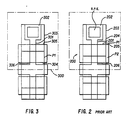
- Figure 2 is a top view of a pair of typical prior art EEPROM memory cells including N+ drain diffusion 201, which is connected via electrical contact 202 to metallization layer 203.
- Cell 200 also includes a first layer of polycrystalline silicon 204 which serves as the floating gate of the EEPROM memory transistor, and a second layer of polycrystalline silicon 205 which serves as the control gate and which forms part of a row line.
- programming, reading, and erasure of cell 200 is all performed from the drain 201 side of the memory cell.
- speed of an EEPROM device is enhanced by utilizing a unique circuit design and operating method which obviates the need for applying a high programming or erase voltage in the path between the memory array and sense amplifier.
- such high programming and erase voltages are applied, as needed, directly to the memory array, thereby allowing all transistors which carry signals from the memory array to the sense amplifier to be fabricated as low voltage devices, thereby increasing their speed of operation and thus the speed of operation of the memory device as a whole.
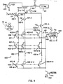
- FIGURE 4 is a schematic diagram of one embodiment of a memory device 400 constructed in accordance with the teachings of this invention.
- Figure 3 is a plan view of a pair of EEPROM memory cells constructed in accordance with the teachings of this invention in which a first layer Pl of polycrystalline silicon forms floating gate 304 located near source 306, rather than near drain 301.
- reading is performed from the drain 301 side of memory cell 300, and programming and erasing performed from the source 306 side of memory cell 300.
- memory device 400 includes row lines 401-1 through 401-N, bit lines 402-1 through 402-M, column select transistors 104-1 through 104-M, and memory array transistors 405-1-1 through 405-N-M.
- Block select transistor 406 is utilized to access the block of memory cells 405-1-1 through 405-N-M.
- memory cell transistors 405-1-1 through 405-N-M are fabricated such that their floating gates are located near their sources, rather than near their drains.
- V DSAT the drain saturation voltage
- V GS the gate-to-source voltage
- V T the threshold voltage
- the read current is limited by the floating gate voltage, which is typically 60 to 70% of the control gate voltage.
- the floating gate voltage typically 60 to 70% of the control gate voltage.
- the read current through the selected memory cell during the read operation is increased since the saturation voltage V DSAT is increased since the drain is influenced by the control gate voltage, rather than the lesser floating gate voltage.
- reading speed is increased. It has been determined that placing the floating gate near the source rather than near the drain increases the read current by about 10 to 15 percent.
- increased speed is also provided due to the fact that column read voltages may be increased, thereby additionally providing increased read current through a selected array transistor, without risking undesirable "soft" writes of the memory cell being read, since the higher read voltage is applied to the drain which is not located near the floating gate.
- undesirable charging may cause a cumulative charge to be placed on the floating gate of a deselected transistor, thereby causing a "soft" write.
- P+ (e.g., Boron) ion implants need not be made to the drains of the memory array transistors as is often the case in prior art structures for enhancing the ability to program the cell, since having a P+N+ junction rather than a P-N+ junction increases the maximum field at the junction leading to greater hot electron generation.
- ion implants can be used on the source side of the memory array transistors where, in accordance with the teachings of this invention, programming occurs by charging the floating gate. By avoiding ion implants on the drains of the memory array transistors, bit line capacitance is reduced, thereby increasing reading speed.
- the P type field implant is not performed near the source of the memory cell transistors, thus increasing the gated diode breakdown voltage of the source junction, which in turn allows greater voltages to be applied to the source in order to improve the performance of the Fowler Nordheim electron tunnelling between the source and the floating gate, as well as decreasing susceptibility of the junction to breakdown.
- Fowler Nordheim tunnelling is independent of temperature and is effective only at high electric fields (typically 7 to 10 Megavolts per centimeter).
- Programming of a selected memory array transistor is performed by applying programming voltage VPP to a selected row line while holding deselected row lines at zero volts, and applying programming voltage VPP through transistor 443 to the sources of all memory array transistors.
- a selected column is grounded by turning on its associated column select transistor, and block select transistor 406 and transistor 421. This causes electrons to be tunneled from the source to the floating gate of the selected transistor.
- programming set transistors 432-1 through 432-M and programming reset transistors 423-1 through 423-M are utilized to minimize the potential for soft programming cells along the selected row line but along deselected columns, which are left floating and thus may be undesirably charged by current flowing from its source to its drain.
- such soft writing is avoided by precharging the deselected bit lines, thereby preventing current from flowing through deselected memory array transistors, which in turn prevents any amount of charging of the floating gates of deselected transistors during the programming of a selected memory array transistor.
- programming a selected memory array cell for example transistor 405-1-1, is performed by first applying a PRGSET signal to lead 432, thus turning on precharge transistors 432-1 through 432-M which apply a predefined voltage (for example, 10 volts) to bit lines 402-1 through 402-M, respectively.
- the PRGSET signal then goes low, turning off transistors 432-1 through 432-M while leaving bit lines 402-1 through 402-M precharged.
- Transistor 421 is then turned on, thereby causing selected bit line 402-1 to be discharged through conducting column select transistor 104-1 and block select transistor 406.
- the deselected columns 402-2 through 402-M remain precharged since their column select transistors 104-2 through 104-M are turned off.
- Source pull down transistor 442 is turned off, and programming voltage VPP is applied through transistor 443 to the sources of all memory array transistors 405-1-1 through 405-N-M.
- Selected memory array transistor 405-1-1 conducts current from its source to its drain, thereby placing a charge on its floating gate.
- bit lines 402-2 through 402-M are discharged by applying a PRG reset signal to lead 422, thus turning on reset transistors 423-1 through 423-M.
- reset transistors 423-1 through 423-M are not used, and the bit lines are discharged by enabling all column select transistors 104-1 through 104-M while transistor 421 is turned on.
- Table 2 reflects, similar to table 1, the programming, reading , and erasure modes of the memory device according to the present invention.
- Row line (control gate) selected VCC (5 volts) deselected: 0 volts bit line (drain) precharged to V ref -V T (typically 1.5 volts) logical 1 stored: pulled low by array transistor, by at least 0.2 volts from precharged level logical 0 stored: not pulled low by array transistor erase line (source) : 0 volts
- Row line (control gate) 0 volts bit line (drain) : 17 volts erase line (source) : Floating
- Row line (control gate) selected VCC (5 volts) deselected : 0 bit line (drain) logical 0 stored: 2 volts logical 1 stored: 1.8 volts erase line (source) : 0
Abstract
Description
- This invention pertains to memory devices and more particularly to flash erase EEPROM memories.
- Electrically erasable programmable read only memories (EEPROMs) are well known in the art. EEPROMs, like other memory devices, include a plurality of memory cells, each capable of storing a single binary digit (bit). The binary value stored in each cell is programmed to a logical zero or logical one value by placing an appropriate charge on the floating gate of a MOS transistor forming the cell. By altering the charge stored on the floating gate, the threshold voltage required to be applied to the control gate of the floating gate transistor is changed to either a voltage level representing a logical one or a voltage level representing a logical zero. When the memory cell is accessed for reading, a voltage is applied to the control gate which is greater than the threshold voltage associated with a logical one but less than the threshold voltage associated with a logical zero. In this manner, with a read signal applied to the control gate, the floating gate transistor turns on if it stores a logical one, but remains off if it stores a logical zero. A sense amplifier, well known in the art, is used to determine if the transistor is on or off.
- FIGURE 1 is a schematic diagram of a typical prior art EEPROM. The circuit of Figure 1 allows for flash erasure of all bits stored in the memory array, that is to say the cells are written on a bit-by-bit, or word-by-word basis, the array is read on a word-by-word basis, and the array is erased by erasing all cells simultaneously to the logical one state. As shown in Figure 1, flash
erase EEPROM circuit 100 includes a plurality of row lines 101-1 through 101-N, and a plurality of columns or "bit lines" 102-1 through 102-M. Associated with each combination of row line and bit line is one of floating gate memory cell transistors 105-1-1 through 105-N-M. The control gates of each memory cell transistor 105-1-1 through 105-N-M are connected to their associated row lines 101-1 through 101-N. The drains of each memory cell transistor are connected to their associated bit lines. The sources of each memory cell transistor are connected in common to the drain oferase transistor 112, as is more fully described later. - Power is supplied to each bit line 102-1 through 102-M through column select transistors 104-1 through 104-M, each receiving an appropriate column select signal on their gate leads 103-1 through 103-M, respectively. The entire block of array transistors 105-1-1 through 105-N-M is selected by
block transistor 106 receiving a block select signal (for example, a decoded signal based on one or more most significant address bits, with the least significant address bits defining individual memory cells within the block) applied to itsgate lead 107. When blockselect transistor 106 is turned on, the block containing memory cells 105-1-1 through 105-N-M is selected and when one or more column select transistors 104-1 through 104-M are turned on, desired ones of bit lines 102-1 through 102-M are selected. This enables the appropriate voltages to be applied to desired ones of bit lines of 102-1 through 102-M. - For example, a programming voltage VPP (typically 12 volts during programming and 17 volts during erasure) is selectively applied to selected bit lines when programming/
erase control circuitry 119 provides a signal to the gate of programming/erase transistor 108 causing transistor 108 to conduct. Similarly, during the read operation, the voltage level of a selected bit line is applied viatransistor 110 to senseamplifier 111 in order to determine the value of the bit stored in a selected memory cell. - The operation of
circuit 100 in the programming, reading, and erasure modes is depicted in Table 1. During programming, memory array transistors are written individually by selectively addressing desired rows and columns. Thus, a selected row receives a voltage (typically approximately 14 volts) thereby enabling the memory transistors within the row to turn on. At the same time, deselected rows each receive a logical zero, preventing the memory transistors of the deselected rows from turning on. For those memory cells within the selected row which are to store a logical one (floating gate uncharged, relatively low control gate threshold voltage), their associated bit lines receive a logical zero by causing their associated column select transistors 104-1 through 104-M to remain off. In other words, columns whose memory cells are to store a logical one are deselected. Conversely, columns associated with memory cells which are to store a logical zero are selected by turning on their associated column select transistors 104-1 through 104-M, and programming/erase control circuitry 119 causes transistor 108 to turn on, thereby applying programming voltage VPP to the selected columns. This action causes the memory transistors which are to store a logical one to turn on and, with a relatively high voltage VPP applied to their drains, 0 volts on their sources, and a high voltage (typically 14 volts) applied to the control gate, cause hot electrons to be injected from the drain to the floating gate, thereby increasing the control gate threshold voltage to that threshold voltage associated with a logical zero. - During reading of
circuit 100, individual memory cells are selected by an appropriate combination of column select and row select signals, allowing the data stored in the selected memory cell to be detected bysense amplifier 111. Thus, for example, to read the data stored in memory cell 105-1-1, row line 101-1 is selected by applying voltage VCC of approximately 5 volts with row lines 101-2 through 101-N being deselected by applying zero volts. Bit line 102-1 is selected by causing column select transistor 104-1 to turn on, while deselecting bit lines 102-2 through 102-M by causing column select transistors 104-2 through 104-M to be turned off. During the read operation, programming/erase transistor 108 is turned off, and a reference voltage VREF (typically 2.5 volts) is applied to the gate ofpass transistor 110. This causes the voltage on the selected bit line 102-1 to be applied to the input lead ofsense amplifier 111, which in turn provides an output signal indicating whether the selected memory cell 105-1-1 stores a logical zero or a logical one. - When memory cell 105-1-1 stores a logical one, its control gate threshold voltage is less than the read voltage applied to row line 101-1, and thus memory cell transistor 105-1-1 is turned on pulling the input lead of
sense amplifier 111 low throughtransistors sense amplifier 111 is not pulled low. Thus,sense amplifier 111 can detect the two possible values of the bits stored by the memory selected for reading. - During erasure, memory cells 105-1-1 through 105-N-M are "flash" erased, i.e., all erased simultaneously such that they store logical zeros. This is accomplished by applying 0 volts to the row lines connected to the control gates of the memory transistors, a high voltage (typically 17 volts) to the bit lines connected to the drains of the memory cell transistors, and leaving the erase line, which is connected to the sources of the memory cell transistors, floating.
- Of importance, during programming and erasing of memory cells 105-1-1 through 105-N-M, a relatively high voltage VPP is applied to selected bit lines 102-1 through 102-M. This requires all transistors between
VPP terminal 120 and bit lines 102-1 through 102-M, as well astransistor 110 located betweenVPP terminal 120 and the input lead ofsense amplifier 111, to be fabricated to ensure they will not break down due to the use of the relatively high voltage VPP. MOS transistors utilized in this fashion, when subjected to relatively high voltages, are subject to gated diode breakdown which, of course, must be eliminated if the device is to operate properly and be reliable over a long period of time. A gated diode is a PN junction located under the gate electrode. When the gate electrode is grounded, the breakdown voltage of the gated diode is much lower than the breakdown voltage of the gated diode when the gate is not grounded. Furthermore, the gated diode breakdown voltage is lower with thinner gate oxides and shallower junctions depths. In order to prevent such gated diode breakdown problems, these transistors are typically formed utilizing a relatively thick gate oxide (typically 350Å thick) as compared with the relatively thin gate oxide utilized by the peripheral transistors in the speed path, such as the transistors (not shown) ofsense amplifier 111, and the transistors of the address buffers, also not shown, which typically have gate oxide thicknesses on the order of 250Å. While the use of thick gate oxide satisfies the requirement that these transistors be impervious to breakdown problems when a high programming/erasure voltage VPP is applied, it has a deleterious effect of decreasing the gain of these transistors, which in turn decreases their switching speed. A decreased switching speed of any transistors located betweensense amplifier 111 and the memory array transistors 105-1-1 through 105 N-M decreases the speed of operation of the device, clearly an undesirable feature. - Figure 2 is a top view of a pair of typical prior art EEPROM memory cells including
N+ drain diffusion 201, which is connected viaelectrical contact 202 tometallization layer 203.Cell 200 also includes a first layer ofpolycrystalline silicon 204 which serves as the floating gate of the EEPROM memory transistor, and a second layer ofpolycrystalline silicon 205 which serves as the control gate and which forms part of a row line. As described above with regard to the schematic diagram of Figure 1, programming, reading, and erasure ofcell 200 is all performed from thedrain 201 side of the memory cell. The drawbacks discussed above are overcome by the present invention as defined in the independent and dependent claims. - In accordance with the teachings of this invention, speed of an EEPROM device is enhanced by utilizing a unique circuit design and operating method which obviates the need for applying a high programming or erase voltage in the path between the memory array and sense amplifier. In accordance with the teachings of this invention, such high programming and erase voltages are applied, as needed, directly to the memory array, thereby allowing all transistors which carry signals from the memory array to the sense amplifier to be fabricated as low voltage devices, thereby increasing their speed of operation and thus the speed of operation of the memory device as a whole. By applying the relatively high programming and erase voltages to the source of the memory transistors, and reading from the drain of the memory transistors, the source and drain, as well as associated circuitry, are fabricated to optimize their intended functions.
- These and other features and advantages of the invention will be more readily apparent upon reading the following description of a preferred exemplified embodiment of the invention and upon reference to the accompanying drawings wherein:
- Figure 1 is a schematic diagram of a typical prior art flash erase EEPROM device;
- Figure 2 is a plan view of a typical prior art EEPROM cell;
- Figure 3 is a plan view of an EEPROM cell constructed in accordance with the teachings of this invention;
- Figure 4 is a schematic diagram of one embodiment of a flash erase EEPROM constructed in accordance with the teaching of this invention; and
- Figure 5 is a schematic diagram of another embodiment of a flash erase EEPROM constructed in accordance with the teachings of this invention.
- FIGURE 4 is a schematic diagram of one embodiment of a
memory device 400 constructed in accordance with the teachings of this invention. Figure 3 is a plan view of a pair of EEPROM memory cells constructed in accordance with the teachings of this invention in which a first layer Pl of polycrystalline silicon forms floatinggate 304 located nearsource 306, rather than neardrain 301. In this embodiment, reading is performed from thedrain 301 side ofmemory cell 300, and programming and erasing performed from thesource 306 side ofmemory cell 300. - Referring now to Figure 4,
memory device 400 includes row lines 401-1 through 401-N, bit lines 402-1 through 402-M, column select transistors 104-1 through 104-M, and memory array transistors 405-1-1 through 405-N-M. Blockselect transistor 406 is utilized to access the block of memory cells 405-1-1 through 405-N-M. In contrast to the prior art, as depicted in FIGURE 1, memory cell transistors 405-1-1 through 405-N-M are fabricated such that their floating gates are located near their sources, rather than near their drains. This allows high programming and erase voltages to be applied to the sources of memory array transistors 405-1-1 through 405-N-M, thereby precluding the application of high programming/erase voltage VPP from blockselect transistor 406 and column select transistors 104-1 through 104-M and passtransistor 410. Therefore these transistors located between bit lines 402-1 and 402-M andsense amplifier 411 need not be fabricated to ensure a high breakdown voltage; thus these transistors can be fabricated utilizing a relatively thin (typically approximately 250Å) gate oxide ensuring high gain and fast switching speed. - It is desirable to increase the read current through a selected memory cell during the read operation in order to provide faster speed of operation and a greater noise immunity. The read current is dependent on the drain saturation voltage VDSAT, which is defined as:
VDSAT ≃ VGS - VT;
where
VDSAT = the drain saturation voltage;
VGS = the gate-to-source voltage; and
VT = the threshold voltage. - In prior art devices, where the floating gate is located near the drain, the read current is limited by the floating gate voltage, which is typically 60 to 70% of the control gate voltage. However, in accordance with the teachings of this invention, by placing the floating gate close to the source rather than the drain as in the prior art, the read current through the selected memory cell during the read operation is increased since the saturation voltage VDSAT is increased since the drain is influenced by the control gate voltage, rather than the lesser floating gate voltage. By increasing the read current, reading speed is increased. It has been determined that placing the floating gate near the source rather than near the drain increases the read current by about 10 to 15 percent.
- In accordance with the teachings of this invention, increased speed is also provided due to the fact that column read voltages may be increased, thereby additionally providing increased read current through a selected array transistor, without risking undesirable "soft" writes of the memory cell being read, since the higher read voltage is applied to the drain which is not located near the floating gate. As is well known, over a large number of read cycles, undesirable charging may cause a cumulative charge to be placed on the floating gate of a deselected transistor, thereby causing a "soft" write.
- Furthermore, utilizing the memory array transistors of this invention, more P+ (e.g., Boron) ion implants need not be made to the drains of the memory array transistors as is often the case in prior art structures for enhancing the ability to program the cell, since having a P+N+ junction rather than a P-N+ junction increases the maximum field at the junction leading to greater hot electron generation. However, such ion implants can be used on the source side of the memory array transistors where, in accordance with the teachings of this invention, programming occurs by charging the floating gate. By avoiding ion implants on the drains of the memory array transistors, bit line capacitance is reduced, thereby increasing reading speed.
- In one embodiment of this invention, the P type field implant is not performed near the source of the memory cell transistors, thus increasing the gated diode breakdown voltage of the source junction, which in turn allows greater voltages to be applied to the source in order to improve the performance of the Fowler Nordheim electron tunnelling between the source and the floating gate, as well as decreasing susceptibility of the junction to breakdown. As is well known, Fowler Nordheim tunnelling is independent of temperature and is effective only at high electric fields (typically 7 to 10 Megavolts per centimeter). Such a pull back of the field implant in order to improve Fowler Nordheim tunnelling from the drains was not possible in the prior art since the pull back of the field implant would have to be performed around the drains of the memory array transistors, which would undesirably degrade the isolation between bit lines and have a deleterious effect on the ability to program memory array transistors due to increased leakage currents leading to lower programming currents.
- Programming of a selected memory array transistor is performed by applying programming voltage VPP to a selected row line while holding deselected row lines at zero volts, and applying programming voltage VPP through
transistor 443 to the sources of all memory array transistors. A selected column is grounded by turning on its associated column select transistor, and blockselect transistor 406 andtransistor 421. This causes electrons to be tunneled from the source to the floating gate of the selected transistor. - In the embodiment of FIG. 5, programming set transistors 432-1 through 432-M and programming reset transistors 423-1 through 423-M are utilized to minimize the potential for soft programming cells along the selected row line but along deselected columns, which are left floating and thus may be undesirably charged by current flowing from its source to its drain.
- In the embodiment of FIG. 5, such soft writing is avoided by precharging the deselected bit lines, thereby preventing current from flowing through deselected memory array transistors, which in turn prevents any amount of charging of the floating gates of deselected transistors during the programming of a selected memory array transistor. In the embodiment of FIG. 5, programming a selected memory array cell, for example transistor 405-1-1, is performed by first applying a PRGSET signal to lead 432, thus turning on precharge transistors 432-1 through 432-M which apply a predefined voltage (for example, 10 volts) to bit lines 402-1 through 402-M, respectively. The PRGSET signal then goes low, turning off transistors 432-1 through 432-M while leaving bit lines 402-1 through 402-M precharged.
Transistor 421 is then turned on, thereby causing selected bit line 402-1 to be discharged through conducting column select transistor 104-1 and blockselect transistor 406. The deselected columns 402-2 through 402-M remain precharged since their column select transistors 104-2 through 104-M are turned off. Source pull downtransistor 442 is turned off, and programming voltage VPP is applied throughtransistor 443 to the sources of all memory array transistors 405-1-1 through 405-N-M. Selected memory array transistor 405-1-1 conducts current from its source to its drain, thereby placing a charge on its floating gate. However, the remaining, deselected memory array transistors do not conduct current since their drains are connected to precharged bit lines 402-2 through 402-M, thereby preventing any charge from being introduced to their floating gates and preventing soft write errors. When memory array transistor 405-1-1 has been programmed,transistor 443 is turned off andtransistor 442 is turned on, thereby connecting the sources of memory array transistors 405-1-1 through 405-N-M to be connected to ground. Bit lines 402-2 through 402-M are discharged by applying a PRG reset signal to lead 422, thus turning on reset transistors 423-1 through 423-M. In an alternative embodiment, reset transistors 423-1 through 423-M are not used, and the bit lines are discharged by enabling all column select transistors 104-1 through 104-M whiletransistor 421 is turned on. - Table 2 reflects, similar to table 1, the programming, reading , and erasure modes of the memory device according to the present invention.
- Although the foregoing invention has been described in some detail by way of illustration and example for purposes of clarity of understanding, it will be readily apparent to those of ordinary skill in the art in light of the teachings of this application that certain changes and modifications may be practiced within the scope of the appended claims.
- Row line (control gate)
selected : 14 volts
deselected: 0 volts
bit line (drain)
logical 1: 0 volts (column deselected)
logical 0: VPP = 9 volts (column selected)
erase line (source) : 0 volts - Row line (control gate)
selected : VCC (5 volts)
deselected: 0 volts
bit line (drain) precharged to Vref-VT (typically 1.5 volts)
logical 1 stored: pulled low by array transistor, by at least 0.2 volts from precharged level
logical 0 stored: not pulled low by array transistor
erase line (source) : 0 volts - Row line (control gate) : 0 volts
bit line (drain) : 17 volts
erase line (source) : Floating - Row line (control gate)
selected : VPP = 14 volts
deselected: 0 volts
bit line (drain)
logical 0 :
selected: approximately 0 volts
deselected: approximately 9 volts volts
logical 1 : 0 volts
erase line (source) : VSP = 9 volts - Row line (control gate)
selected : VCC (5 volts)
deselected : 0
bit line (drain)
logical 0 stored: 2 volts
logical 1 stored: 1.8 volts
erase line (source) : 0 - Row line (control gate) : 0 volts
bit line (drain) : Floating
erase line (source) : VEE = 17 volts
Claims (28)
a memory cell comrpising:
a source region;
a drain region located apart from said source region;
a channel region located between said source and said drain regions;
a floating gate electrode above said channel region sufficiently close to said source region to allow charge transfer between said floating gate electrode and that portion of said channel region adjacent said source region, and sufficiently distant from said drain region to prevent charge transfer between said floating gate electrode and that portion of said channel region adjacent said drain region;
a control gate electrode located above said channel region and said floating gate electrode and separated from said channel region and said floating gate electrode by a second dielectric layer;
programming means connected to said source region for selectively causing a change in the charge stored on said floating gate electrode, thereby altering the control gate threshold voltage of said memory cell; and
reading means connected to said drain region for deter,mining the amount of current flow through said channel region in response to the application of a set of read voltages to said control gate electrode, source region, and drain region.
a plurality of bit lines;
a plurality of word lines;
bit line addressing means for selecting a desired one of said bit lines and deselecting the remaining bit lines;
word line addressing means for selecting a desired one of said word lines and deselecting the remaining word lines;
a plurality of memory cells, each uniquely associated with a bit line-word line pair, each said memory cell comprising:
a source region;
a drain region located apart from said source region and connected to the bit line associated with said memory cell;
a channel region located between said source and said drain regions;
a floating gate electrode located above said channel region near said source region and not near said drain region, said floating gate electrode separated from said channel by a first dielectric layer;
a control gate electrode located above said channel region and said floating gate electrode and separated from said channel region and said floating gate electrode by a second dielectric layer, said control gate electrode being connected to the word line associated with said memory cell;
programming means for applying a programming potential between said source region and said word line of a selected memory cell in order to selectively cause a change in the charge stored on said floating gate electrode of said selected memory cell, thereby altering the control gate threshold voltage of said selected memory cell; and
a sense amplifier having an input lead connected to said selected bit line and having an output lead for providing an output signal indicative of the data stored in said selected memory cell.
a precharge source for providing a precharge potential; and
a plurality of precharge transistors, each uniquely associated with one of said bit lines, and having a source connected to said bit line, a drain connected to said precharge source, and a control gate connected to means for providing a precharge control signal.
forming a source region in a semiconductor material;
forming a drain region in said semiconductor material and located apart from said source region, thereby forming a channel region between said source and said drain regions;
forming a first layer of dielectric above said channel region;
forming a floating gate electrode above said channel region sufficiently close to said source region to allow charge transfer between said floating gate electrode and that portion of said channel region adjacent said source region, and sufficiently distant from said drain region to prevent charge transfer between said floating gate electrode and that portion of said channel region adjacent said drain region;
forming a second layer of dielectric above said floating gate electrode; and
forming a control gate electrode above said second layer of dielectric.
a source region;
a drain region located apart from said source region;
a channel region located between said source and said drain regions;
a floating gate electrode located above said channel region sufficiently close to said source region to allow charge transfer between said floating gate electrode and that portion of said channel region adjacent said source region, and sufficiently distant from said drain region to prevent charge transfer between said floating gate electrode and that portion of said channel region adjacent said drain region, said floating gate electrode separated from said channel by a first dielectric layer; and
a control gate electrode located above said channel region and said floating gate electrode and separated from said channel region and said floating gate electrode by a second dielectric layer, said method comprising the steps of:
applying a set of programming voltages to said control gate electrode and said source region in order to cause a change in the charge stored on said floating gate electrode, thereby storing data in said memory device by altering the control gate threshold voltage of said memory device; and
sensing at said drain region the current flow through said channel region in response to a set of read voltages applied to said control gate electrode, source region, and drain region, thereby determining the state of said data stored in said memory device.
Applications Claiming Priority (2)
| Application Number | Priority Date | Filing Date | Title |
|---|---|---|---|
| US275380 | 1988-11-23 | ||
| US07/275,380 US4999812A (en) | 1988-11-23 | 1988-11-23 | Architecture for a flash erase EEPROM memory |
Publications (2)
| Publication Number | Publication Date |
|---|---|
| EP0370416A2 true EP0370416A2 (en) | 1990-05-30 |
| EP0370416A3 EP0370416A3 (en) | 1990-12-05 |
Family
ID=23052047
Family Applications (1)
| Application Number | Title | Priority Date | Filing Date |
|---|---|---|---|
| EP19890121391 Withdrawn EP0370416A3 (en) | 1988-11-23 | 1989-11-18 | Novel architecture for a flash erase eprom memory |
Country Status (4)
| Country | Link |
|---|---|
| US (1) | US4999812A (en) |
| EP (1) | EP0370416A3 (en) |
| JP (1) | JPH03155667A (en) |
| KR (1) | KR0155357B1 (en) |
Families Citing this family (27)
| Publication number | Priority date | Publication date | Assignee | Title |
|---|---|---|---|---|
| DE69129492T2 (en) * | 1990-10-02 | 1998-11-05 | Toshiba Kk | SEMICONDUCTOR MEMORY |
| US5241507A (en) * | 1991-05-03 | 1993-08-31 | Hyundai Electronics America | One transistor cell flash memory assay with over-erase protection |
| US5541878A (en) * | 1991-05-09 | 1996-07-30 | Synaptics, Incorporated | Writable analog reference voltage storage device |
| US5166562A (en) * | 1991-05-09 | 1992-11-24 | Synaptics, Incorporated | Writable analog reference voltage storage device |
| JP3375087B2 (en) * | 1991-10-21 | 2003-02-10 | ローム株式会社 | Semiconductor memory device and storage information reading method thereof |
| US5293328A (en) * | 1992-01-15 | 1994-03-08 | National Semiconductor Corporation | Electrically reprogrammable EPROM cell with merged transistor and optiumum area |
| FR2688333B1 (en) * | 1992-03-06 | 1994-04-29 | Sgc Thomson Microelectronics S | DEVICE AND METHOD FOR DELETING BY SECTORS OF A FLASH EPROM MEMORY. |
| KR960006748B1 (en) * | 1993-03-31 | 1996-05-23 | 삼성전자주식회사 | Nonvolatile semiconductor integrated circuit device |
| DE69305986T2 (en) * | 1993-07-29 | 1997-03-06 | Sgs Thomson Microelectronics | Circuit structure for memory matrix and corresponding manufacturing processes |
| US5427963A (en) * | 1993-12-10 | 1995-06-27 | Advanced Micro Devices, Inc. | Method of making a MOS device with drain side channel implant |
| US5376573A (en) * | 1993-12-10 | 1994-12-27 | Advanced Micro Devices, Inc. | Method of making a flash EPROM device utilizing a single masking step for etching and implanting source regions within the EPROM core and redundancy areas |
| US5581485A (en) * | 1994-12-08 | 1996-12-03 | Omni Microelectronics, Inc. | Analog vector distance measuring and vector quantization architecture |
| US5920296A (en) * | 1995-02-01 | 1999-07-06 | Pixel International | Flat screen having individually dipole-protected microdots |
| US5801076A (en) * | 1995-02-21 | 1998-09-01 | Advanced Micro Devices, Inc. | Method of making non-volatile memory device having a floating gate with enhanced charge retention |
| KR0172403B1 (en) * | 1995-11-15 | 1999-03-30 | 김광호 | Data read circuit of non-volatile semiconductor memory |
| US5828603A (en) * | 1997-04-23 | 1998-10-27 | Atmel Corporation | Memory device having a power supply-independent low power consumption bit line voltage clamp |
| JPH10312694A (en) * | 1997-05-08 | 1998-11-24 | Oki Electric Ind Co Ltd | Semiconductor non-volatile memory and power source circuit therefor |
| US6175520B1 (en) | 1997-05-30 | 2001-01-16 | Alliance Semiconductor Corporation | Nonvolatile memory array having local program load line repeaters |
| US6031765A (en) * | 1999-04-22 | 2000-02-29 | Aplus Flash Technology, Inc. | Reversed split-gate cell array |
| US6181607B1 (en) | 1999-04-22 | 2001-01-30 | Aplus Flash Technology, Inc. | Reversed split-gate cell array |
| US6977841B2 (en) * | 2002-11-21 | 2005-12-20 | Micron Technology, Inc. | Preconditioning of defective and redundant columns in a memory device |
| US8324667B2 (en) * | 2004-01-05 | 2012-12-04 | International Business Machines Corporation | Amplifiers using gated diodes |
| US7116594B2 (en) * | 2004-09-03 | 2006-10-03 | International Business Machines Corporation | Sense amplifier circuits and high speed latch circuits using gated diodes |
| JP4642030B2 (en) * | 2004-09-30 | 2011-03-02 | スパンション エルエルシー | Semiconductor device and control method thereof |
| US20090307140A1 (en) | 2008-06-06 | 2009-12-10 | Upendra Mardikar | Mobile device over-the-air (ota) registration and point-of-sale (pos) payment |
| US7995384B2 (en) | 2008-08-15 | 2011-08-09 | Macronix International Co., Ltd. | Electrically isolated gated diode nonvolatile memory |
| US8862767B2 (en) | 2011-09-02 | 2014-10-14 | Ebay Inc. | Secure elements broker (SEB) for application communication channel selector optimization |
Citations (2)
| Publication number | Priority date | Publication date | Assignee | Title |
|---|---|---|---|---|
| US4462090A (en) * | 1978-12-14 | 1984-07-24 | Tokyo Shibaura Denki Kabushiki Kaisha | Method of operating a semiconductor memory circuit |
| EP0182198A2 (en) * | 1984-11-21 | 1986-05-28 | Rohm Corporation | Single transistor electrically programmable device and method |
Family Cites Families (1)
| Publication number | Priority date | Publication date | Assignee | Title |
|---|---|---|---|---|
| US4852062A (en) * | 1987-09-28 | 1989-07-25 | Motorola, Inc. | EPROM device using asymmetrical transistor characteristics |
-
1988
- 1988-11-23 US US07/275,380 patent/US4999812A/en not_active Expired - Fee Related
-
1989
- 1989-11-18 EP EP19890121391 patent/EP0370416A3/en not_active Withdrawn
- 1989-11-22 KR KR1019890016950A patent/KR0155357B1/en not_active IP Right Cessation
- 1989-11-24 JP JP1303482A patent/JPH03155667A/en active Pending
Patent Citations (2)
| Publication number | Priority date | Publication date | Assignee | Title |
|---|---|---|---|---|
| US4462090A (en) * | 1978-12-14 | 1984-07-24 | Tokyo Shibaura Denki Kabushiki Kaisha | Method of operating a semiconductor memory circuit |
| EP0182198A2 (en) * | 1984-11-21 | 1986-05-28 | Rohm Corporation | Single transistor electrically programmable device and method |
Non-Patent Citations (1)
| Title |
|---|
| PROCEEDINGS OF THE IEEE 1988 CUSTOM INTEGRATED CIRCUITS CONFERENCE, Rochester, New York, 16th - 19th May 1988, pages 4.1.1 - 4.1.4, IEEE, New York, US; T. MARUYAMA et al.: "Wide operating voltage range and low power consumption EPROM structure for consumer oriented ASIC applications" * |
Also Published As
| Publication number | Publication date |
|---|---|
| EP0370416A3 (en) | 1990-12-05 |
| JPH03155667A (en) | 1991-07-03 |
| US4999812A (en) | 1991-03-12 |
| KR900008528A (en) | 1990-06-04 |
| KR0155357B1 (en) | 1998-12-01 |
Similar Documents
| Publication | Publication Date | Title |
|---|---|---|
| US4999812A (en) | Architecture for a flash erase EEPROM memory | |
| US5511022A (en) | Depletion mode NAND string electrically erasable programmable semiconductor memory device and method for erasing and programming thereof | |
| EP0545904B1 (en) | Nonvolatile semiconductor memory device | |
| US5596525A (en) | Memory cell of nonvolatile semiconductor memory device | |
| US5812452A (en) | Electrically byte-selectable and byte-alterable memory arrays | |
| US5270969A (en) | Electrically programmable nonvolatile semiconductor memory device with nand cell structure | |
| KR0170707B1 (en) | Non-volatile memory device and its driving method | |
| US5666307A (en) | PMOS flash memory cell capable of multi-level threshold voltage storage | |
| US4366555A (en) | Electrically erasable programmable read only memory | |
| KR20010030062A (en) | Nonvolatile semiconductor memory | |
| JP2633252B2 (en) | Semiconductor storage device | |
| EP0025155A2 (en) | Nonvolatile semiconductor memory device | |
| KR0172422B1 (en) | Common source line control circuit | |
| EP0656627A2 (en) | An adjustable threshold voltage circuit | |
| JPH05159589A (en) | Single-transistor-cell flash memory array having excessive-erase protecting function | |
| US7995399B2 (en) | NAND memory device and programming methods | |
| EP0387889B1 (en) | Nonvolatile semiconductor memory | |
| KR19990014206A (en) | Nonvolatile Semiconductor Memory | |
| US6420753B1 (en) | Electrically selectable and alterable memory cells | |
| US6011717A (en) | EEPROM memory programmable and erasable by Fowler-Nordheim effect | |
| KR19990013057A (en) | Read and write method of flash memory device for selectively storing single bit data and multiple bit data on same chip | |
| US5943268A (en) | Non-volatile latch having PMOS floating gate memory cells | |
| JPH0314272A (en) | Nonvolatile semiconductor storage device | |
| JPH0512889A (en) | Nonvolatile semiconductor storage | |
| KR0165468B1 (en) | Semiconductor memory device & fabrication method & operation method |
Legal Events
| Date | Code | Title | Description |
|---|---|---|---|
| PUAI | Public reference made under article 153(3) epc to a published international application that has entered the european phase |
Free format text: ORIGINAL CODE: 0009012 |
|
| AK | Designated contracting states |
Kind code of ref document: A2 Designated state(s): DE FR GB IT NL |
|
| PUAL | Search report despatched |
Free format text: ORIGINAL CODE: 0009013 |
|
| AK | Designated contracting states |
Kind code of ref document: A3 Designated state(s): DE FR GB IT NL |
|
| 17P | Request for examination filed |
Effective date: 19910508 |
|
| 17Q | First examination report despatched |
Effective date: 19930308 |
|
| STAA | Information on the status of an ep patent application or granted ep patent |
Free format text: STATUS: THE APPLICATION IS DEEMED TO BE WITHDRAWN |
|
| 18D | Application deemed to be withdrawn |
Effective date: 19960501 |