EP0372045B1 - Metering pulse generators - Google Patents
Metering pulse generators Download PDFInfo
- Publication number
- EP0372045B1 EP0372045B1 EP89905966A EP89905966A EP0372045B1 EP 0372045 B1 EP0372045 B1 EP 0372045B1 EP 89905966 A EP89905966 A EP 89905966A EP 89905966 A EP89905966 A EP 89905966A EP 0372045 B1 EP0372045 B1 EP 0372045B1
- Authority
- EP
- European Patent Office
- Prior art keywords
- spring member
- pulse signal
- generating device
- further characterized
- signal generating
- Prior art date
- Legal status (The legal status is an assumption and is not a legal conclusion. Google has not performed a legal analysis and makes no representation as to the accuracy of the status listed.)
- Expired - Lifetime
Links
Images
Classifications
-
- G—PHYSICS
- G06—COMPUTING; CALCULATING OR COUNTING
- G06M—COUNTING MECHANISMS; COUNTING OF OBJECTS NOT OTHERWISE PROVIDED FOR
- G06M1/00—Design features of general application
- G06M1/27—Design features of general application for representing the result of count in the form of electric signals, e.g. by sensing markings on the counter drum
- G06M1/276—Design features of general application for representing the result of count in the form of electric signals, e.g. by sensing markings on the counter drum using mechanically-actuated contacts
Definitions
- This invention relates to metering pulse generators and more particularly to devices for installation on gas or water meters or the like to develop electrical pulses for transmission to a remote monitoring location.
- Metering pulse generators of the invention supply pulses of controlled amplitude and width, require a very low torque input, have minimal standby power requirements and a long operating life.
- the generators are quite compact and readily installed, are comparatively simple in construction and operation and are manufacturable at low cost.
- the Sears U.S. Patent No. 4,470,010 discloses an apparatus in which a dial arm of a meter engages a shoe which is affixed to one end of a shaft to rotate the shaft against the action of a coiled spring wrapped around the shaft. At its opposite end, the shaft has a striker arm portion which is engageable with a bar of piezoelectric material to generate an impulse. The impulse is transmitted through wires to remotely located circuitry.
- US 3,862,402 shows a flexible probe member which is fixed to a piezoelectronic element. Oscillation of an output signal depends on oscillation of the piezoelectronic element in an initial phase and upon oscillation of the probe in a later phase.
- US 3,962,691 discloses a pulse generating circuit for a metering element in which a cantilevered spring member is part of a mechanical cam follower mechanism. The present invention is directed to a compact arrangement of a cantilevered spring element, a piezoelectronic element and associated circuitry for responding to bending movements of the spring element to generate suitable pulses for metering utility consumption.
- This invention was evolved with the general object of providing metering pulse generators which have minimal energy consumption and which impose minimal mechanical loads on meters on which they are installed, while reliably generating metering pulses for transmission to a remote location. It is also an object of the invention to provide metering pulse generators which have a very compact size and which are easily installed and which are also economically manufacturable.
- a sensor is engaged and deformed by a metering element to develop an electrical signal
- the sensor preferably comprising a deformable spring member with a cantilevered free end and a sensing device directly secured thereto.
- the spring member is of resilient sheet material which is bent through engagement by a metering element and a strip of piezoelectric material is secured to the spring member to generate electrical signals in response to bending thereof.
- Very important features relate to the provision of an amplifier device in close proximity to the sensor and arranged to respond to the electrical signal developed by the sensor to transmit an output pulse signal to a remote location.
- the amplifier device and associated circuit components are mounted directly on the spring member and the spring member is of insulating material and functions as a printed circuit board for connections between the sensor and amplifier device and circuit components.
- the senor is arranged to develop a single high amplitude pulse signal of one polarity and the amplifier device is switched from a non-conductive state to a conductive state in response to each high amplitude pulse signal applied thereto.
- the amplifier device is switched from a non-conductive state to a conductive state in response to each high amplitude pulse signal applied thereto.
- Specific features relate to the development of the single high amplitude pulse signal in a manner such as to insure accurate and reliable metering.
- a bending movement of the spring member is gradually effected away from an initial rest condition and then the spring member is released to effect a rapid return movement to the rest condition.
- the high amplitude pulse is developed during the rapid return movement.
- the piezoelectric sensing device the a charge of one polarity developed during the movement away from the rest condition is allowed to gradually leak away, and the high amplitude pulse is developed in response to a charge of the opposite polarity which is developed during the rapid return movement.
- Oscillations of the member and the possibility of resultant multiple pulse generations are avoiding by damping and absorbing the energy of the spring member as it is rapidly returned to the initial rest position.
- Preferred methods include the absorption of energy in air which is entrapped between the spring member to be pressurized and displaced during the return movement and the provision of a stop structure which is engaged by the spring member to absorb energy and limit any substantial excursion beyond the initial rest condition.
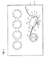
- Reference numeral 10 generally designates a pulse generating device which is constructed in accordance with the principles of this invention.
- the device 10 may be mounted on the face 11 of a gas meter 12 and is designed to produce a pulse in response to each rotation of a dial pointer 13.
- the illustrated device 10 includes a member 14 of resilient sheet material which extends from a housing 15 and which has a terminal end portion 14a engageable by the end of the dial pointer.
- the pointer 13 rotates in a counter-clockwise direction and it engages the member 14 to effect a gradual bending movement of the member 14 away from an initial rest position.
- the pointer 13 reaches a certain angular position, the resiliency of the member operates to effect a relatively rapid return movement of the member to an initial rest position as shown.
- the device 10 generates an electrical pulse signal in response to the rapid return movement of the spring member and has output terminals for connection to a connector 16 at one end of a cable 17, for transmission of the signal to a remote location which may be several feet away.
- the device 10 may be used to transmit metering pulses to an automatic meter reader or "AMR" which is arranged to periodically transmit metering data through a telephone line to a utility control center.
- AMR automatic meter reader
- the AMR is preferably battery operated and it is highly desirable that current consumption be minimized. Accuracy, reliability and a long operating life are also extremely important.
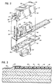
- the housing 15 comprises a bottom cover or base 18 and a top cover 19 both of which may be injection-molded plastic parts. Mounting arrangements may vary in accordance with the type and construction of the particular meter on which the device is mounted.
- a screw 20 has a shank extending through a slot 21 in an integral tab portion 22 of the base 18.
- the slot 21 is elongated in a direction generally parallel to the member 14 and permits accurate adjustment of the positional relationship of the member 14 relative to the path of movement of the end of the meter pointer 13.
- the bottom cover or base 18 also includes an integral tab 24 at one end which extends along the lower side of the member 14 and toward the free terminal end portion 14a thereof.
- the tab 24 operates as a damping means to control the duration of the return movement of the member 14 and to inhibit oscillation thereof. During such return movement, a cushion of air is developed between the member 14 and the tab 24 and is pressurized and displaced to absorb a portion of the energy stored during bending of the member 14 after which the member 14 engages the tab 24 to mechanically absorb the remaining energy.
- a deformation sensing means is secured to the spring member 14, preferably comprising a very thin and lightweight piezoelectric transducer 26 which is adhesively secured to the upper surface of the spring member 14.
- An electronic amplifying device is also provided which is preferably a field-effect transistor 28 mounted on the spring member 14 in close proximity to the transducer 26 and connected thereto through circuitry which is also mounted on the spring member.
- the spring member supports a resistor 29 and a rectangular package 30 which contains two resistors.
- a pair of pins 31 and 32 are provided which form output terminals and which extend upwardly through openings 33 and 34 in a wall portion 35 of the top cover 19 and into the connector 16 of the cable 17.
- the pins 31 and 32 are inserted in holes in the spring member 14 and, when the device is assembled, lower ends of the pins engage in underlying recesses in the base 18, for mechanical support and rigidity.
- the spring member 14 is of an electrically insulating material and forms a printed circuit board with traces of copper or the equivalent formed thereon to provide connections between the transducer 26, transistor 28 and resistor 29 and the resistors in package 30.
- the spring member 14 performs a number of important functions and a very compact assembly is provided.
- the top cover 19 includes an upper wall portion 36 which is overlies the transistor 28, resistor 29 and resistor package 30. Cover 19 may be secured to the base through a connecting screw 37 extended through a central hole 38 in the cover 19 and thence downwardly through a hole in the member 14 and into a hole in the base 18.
- the cover 19 is also formed with a slot 39 in one end wall 40 and a similar slot in the opposite end wall for embracing the spring member 14, and with a pair of notches 41 and 42 in one side wall 43 and similar notches in an opposite side wall for receiving tabs 45 and 46 which project from one side of the member 14 and similar tabs which project from the opposite side of the member 14.
- the member 14 is securely held in position relative to the housing 15.
- the base 18 is formed with recesses 18a and 18b for providing space to receive terminals and portions of the components which project from the underside of the member 14.
- FIG 3 is a cross-sectional view with certain thicknesses exaggerated to show how the transducer 26 is constructed and assembled on the member 14.
- the transducer 26 is in the form of a thin film of a piezoelectrically active material and electrodes secured thereto.
- it may preferably comprise a polyvinylidene fluoride film 48 which is approximately 0.200 inches (5,08 mm) wide by 0.750 inches (19,05 mm) long and 28 microns thick and which has electrodes 49 and 50 silk-screened onto its opposite faces.
- An adhesive 51 is provided between the lower electrode 49 and the upper face of the member 14 to secure the transducer 26 to the member 14.
- the adhesive 51 is a conductive adhesive to also function to provide an electrical connection between the electrode 49 on the lower face of the film 48 and a copper trace 52 on the upper face of the member.
- a connection 53 is similarly provided between the upper electrode 50 and a copper trace 54 on the member 14 which is electrically separate from the trace 52.
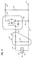
- Figure 4 is a circuit diagram.
- the transistor 26 is an N channel enhancement mode, metal oxide field effect transistor or "MOSFET". It has a drain electrode 55 connected to the pin 32 and to one terminal of the resistor 29 and a source electrode 56 connected to the pin 31, to the other terminal of resistor 29 and also to the transducer electrode 49 through the trace 52.
- a gate electrode 57 is connected to a terminal of one resistor 58 of the package 30, the other terminal of the resistor 58 being connected to the transducer electrode 50 through the trace 54.
- a second resistor 60 of the package 30 is connected between traces 52 and 54, in parallel relation to the transducer 26.
- the film 48 develops a charge between its opposite faces when deformed during bending of the member 14.
- the film 48 is compressed during bending of the member 14 away from its rest position, developing a charge having a polarity such that the voltage of the electrode 50 is negative relative to the electrode 49.
- the polarity of the charge so developed during bending is opposite that required to cause conduction of the transistor 28. Such bending takes place relatively slowly and the charge gradually bleeds off through the resistor 60.
- the charge is changed in the opposite direction and a voltage is developed at the electrode 50 which is of positive polarity and which is such as to cause conduction of the transistor 28 for a certain time interval, dependent upon the amount of deflection and the values and characteristics of the components.
- the voltage at the gate electrode 57 is sufficient to initiate conduction of the transistor 28, the effective resistance between the gate and source electrodes 57 and 56 is relatively low as compared to the resistances of the resistors 58 and 60.
- the electrical values which affect the conduction time are the values of the resistors 58 and 60, the capacitance of the transducer 26 and the voltage generated by the film during deflection, the capacitance of transducer 26 and the generated voltage being a function of the thickness and effective area of the film 48, its composition and the deflection thereof.
- the types and values of the components may be as follows: Reference number Type or value 28 Silconix VN2222L 29 249,000 ohms 58 10 megohms 60 22 megohms
- the film 48 of the transducer may be a polyvinylidene fluoride film marketed by Pennwalt Corporation under the trade name "KYNAR", approximately 0.200 inches (5,08 mm) wide, 0.750 inches (19,05 mm) long and 28 microns in thickness.
- the spring member 14 may be a multilayer epoxy/glass fabric laminate of a type used in conventional circuit boards, approximately 1.5 inches (38,1 mm) long, 0.200 inches (5,08 mm) wide and 0.020 inches (0,508 mm) thick, with copper surface paths on both surfaces and with holes for insertion of the terminals or leads of the transistor and resistor components. After wave soldering of the leads, a conformal coating is applied to protect the assembly from the environment.
- the duration of conduction of the transistor 26 may range from 2 to 20 milliseconds depending upon the deflection of member 14.
- the resistance between the pins 31 and 32 may be on the order of 7.5 ohms during conduction of the transistor 28 and is substantially the same as that of the resistor 29, i.e. 249,000 ohms, during non-conduction of the transistor 28.
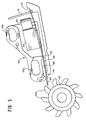
- FIG. 5 is a view illustrating portions of a modified device 62, shown with a cover thereof removed and shown in relation to a rotating meter element 63.
- Element 63 may be an element of a water meter, for example, to be rotated in proportion to the volume of water flowing through a metering mechanism. As shown, it has 10 arcuately spaced cam fingers 64 on its periphery which are engageable with a terminal end portion 65 of a spring member 66 of the device 62.
- Spring member 66 of device 62 is like the member 14 of the device 10 and has transducer and circuit components mounted thereon in the same way, including a piezoelectric film transducer 68 like transducer 26, a field-effect transistor 69 like transistor 28, a pair of resistors in a package 70, corresponding to resistors 58 and 60 in package 30, and an additional resistor which is not seen in Figure but which is like resistor 29 and behind the package 70.
- a pair of pins which are like pins 31 and 32 are secured to member 66 adjacent one end thereof to form output terminals, as indicated by reference numeral 71.
- a housing 72 is provided which is formed with slots 72 a and 72 b for receiving screws to mount the device on the face of a meter.
- the housing 72 is formed to provide a slot for receiving and supporting the member 66 in a slightly bowed configuration when in an initial rest condition thereof, the member 66 being engaged by a shoulder 73 and two ribs 74 and 75 which extend transversely relative to the member 66 at longitudinally spaced positions.
- the shoulder 73 engages the underside of the end portion of the member 66 adjacent the pins 71.
- the rib 74 engages a portion of the spring member 66 which is spaced from the terminal end portion 65 thereof engaged by the cam fingers 64.
- the rib 75 engages the upper side of the member 66 at a position which is intermediate the shoulder 73 and the rib 74, in the longitudinal direction, and is located below a plane through the shoulder 73 and the rib 74, thereby holding the member 66 in a bowed condition.
- each of the cam fingers 64 engages the terminal end portion of the spring member 66 to move the spring member 66 upwardly away from the rib 74, a fulcrum point being provided by the rib 75.
- the member 66 is released to move rapidly back toward the initial rest position as illustrated, and a high amplitude pulse is generated by the transducer 68 of a polarity such as to cause conduction of the transistor 69.
- the spring member 66 engages the rib 74 which absorbs energy and limits any substantial excursion beyond the rest condition.
- the arrangement prevents any deformation of the transducer 68 which might produce a pulse of an amplitude and polarity such as to cause development of a second pulse.
- the result is that a single and very clean high amplitude pulse is generated in response to movement of each cam finger into engagement with the member 66.
Abstract
Description
- This invention relates to metering pulse generators and more particularly to devices for installation on gas or water meters or the like to develop electrical pulses for transmission to a remote monitoring location. Metering pulse generators of the invention supply pulses of controlled amplitude and width, require a very low torque input, have minimal standby power requirements and a long operating life. The generators are quite compact and readily installed, are comparatively simple in construction and operation and are manufacturable at low cost.
- Devices have heretofore been provided for developing pulses in response to rotation of dial arms of gas, water or other utility meters or the like. For example, the Sears U.S. Patent No. 4,470,010 discloses an apparatus in which a dial arm of a meter engages a shoe which is affixed to one end of a shaft to rotate the shaft against the action of a coiled spring wrapped around the shaft. At its opposite end, the shaft has a striker arm portion which is engageable with a bar of piezoelectric material to generate an impulse. The impulse is transmitted through wires to remotely located circuitry.
- The problem to be solved is to provide a device for converting mechanical movements of a metering element to a suitable electrical pulse. US 3,862,402 (D1) shows a flexible probe member which is fixed to a piezoelectronic element. Oscillation of an output signal depends on oscillation of the piezoelectronic element in an initial phase and upon oscillation of the probe in a later phase. US 3,962,691 (D2) discloses a pulse generating circuit for a metering element in which a cantilevered spring member is part of a mechanical cam follower mechanism. The present invention is directed to a compact arrangement of a cantilevered spring element, a piezoelectronic element and associated circuitry for responding to bending movements of the spring element to generate suitable pulses for metering utility consumption.
- This invention was evolved with the general object of providing metering pulse generators which have minimal energy consumption and which impose minimal mechanical loads on meters on which they are installed, while reliably generating metering pulses for transmission to a remote location. It is also an object of the invention to provide metering pulse generators which have a very compact size and which are easily installed and which are also economically manufacturable.
- In accordance with this invention, a sensor is engaged and deformed by a metering element to develop an electrical signal, the sensor preferably comprising a deformable spring member with a cantilevered free end and a sensing device directly secured thereto. Thus, an electrical signal is directly generated in response to movement of the metering element and a simplified and compact device is provided. In preferred embodiments, the spring member is of resilient sheet material which is bent through engagement by a metering element and a strip of piezoelectric material is secured to the spring member to generate electrical signals in response to bending thereof.
- Very important features relate to the provision of an amplifier device in close proximity to the sensor and arranged to respond to the electrical signal developed by the sensor to transmit an output pulse signal to a remote location. Preferably, the amplifier device and associated circuit components are mounted directly on the spring member and the spring member is of insulating material and functions as a printed circuit board for connections between the sensor and amplifier device and circuit components.
- In accordance with another important feature, the sensor is arranged to develop a single high amplitude pulse signal of one polarity and the amplifier device is switched from a non-conductive state to a conductive state in response to each high amplitude pulse signal applied thereto. Thus, there is significant energy consumption only during development of the pulse signal.
- Specific features relate to the development of the single high amplitude pulse signal in a manner such as to insure accurate and reliable metering. In generators constructed in accordance with the invention, a bending movement of the spring member is gradually effected away from an initial rest condition and then the spring member is released to effect a rapid return movement to the rest condition. The high amplitude pulse is developed during the rapid return movement. In particular, with the piezoelectric sensing device, the a charge of one polarity developed during the movement away from the rest condition is allowed to gradually leak away, and the high amplitude pulse is developed in response to a charge of the opposite polarity which is developed during the rapid return movement.
- Oscillations of the member and the possibility of resultant multiple pulse generations are avoiding by damping and absorbing the energy of the spring member as it is rapidly returned to the initial rest position. Preferred methods include the absorption of energy in air which is entrapped between the spring member to be pressurized and displaced during the return movement and the provision of a stop structure which is engaged by the spring member to absorb energy and limit any substantial excursion beyond the initial rest condition.
- This invention contemplates other objects, features and advantages which will become more fully apparent from the following detailed description taken in conjunction with the accompanying drawings.
-
- FIGURE 1 is a front elevational view showing a metering pulse generator of the invention mounted on the face of a gas meter;
- FIGURE 2 is an isometric exploded view, showing the construction of components of the pulse generator of FIG. 1 and the manner of assembly thereof;
- FIGURE 3 is a cross-sectional view on an enlarged scale and with certain thicknesses exaggerated, showing the construction of a piezoelectric film transducer and the mounting thereof on a spring member of the generator;
- FIGURE 4 is a circuit diagram, showing connections of components of the generator; and
- FIGURE 5 is a front elevational view showing a modified metering pulse generator of the invention and diagrammatically showing the mounting thereof on a water meter, but with a cover of the generator removed to show the internal construction.
-
Reference numeral 10 generally designates a pulse generating device which is constructed in accordance with the principles of this invention. As shown in Figure 1, thedevice 10 may be mounted on the face 11 of agas meter 12 and is designed to produce a pulse in response to each rotation of adial pointer 13. The illustrateddevice 10 includes amember 14 of resilient sheet material which extends from ahousing 15 and which has a terminal end portion 14a engageable by the end of the dial pointer. In the arrangement as shown in Figure 1, thepointer 13 rotates in a counter-clockwise direction and it engages themember 14 to effect a gradual bending movement of themember 14 away from an initial rest position. When thepointer 13 reaches a certain angular position, the resiliency of the member operates to effect a relatively rapid return movement of the member to an initial rest position as shown. - The
device 10 generates an electrical pulse signal in response to the rapid return movement of the spring member and has output terminals for connection to aconnector 16 at one end of acable 17, for transmission of the signal to a remote location which may be several feet away. By way of example, thedevice 10 may be used to transmit metering pulses to an automatic meter reader or "AMR" which is arranged to periodically transmit metering data through a telephone line to a utility control center. The AMR is preferably battery operated and it is highly desirable that current consumption be minimized. Accuracy, reliability and a long operating life are also extremely important. - The
housing 15 comprises a bottom cover orbase 18 and atop cover 19 both of which may be injection-molded plastic parts. Mounting arrangements may vary in accordance with the type and construction of the particular meter on which the device is mounted. In the illustrated construction, ascrew 20 has a shank extending through aslot 21 in anintegral tab portion 22 of thebase 18. Theslot 21 is elongated in a direction generally parallel to themember 14 and permits accurate adjustment of the positional relationship of themember 14 relative to the path of movement of the end of themeter pointer 13. - The bottom cover or
base 18 also includes anintegral tab 24 at one end which extends along the lower side of themember 14 and toward the free terminal end portion 14a thereof. Thetab 24 operates as a damping means to control the duration of the return movement of themember 14 and to inhibit oscillation thereof. During such return movement, a cushion of air is developed between themember 14 and thetab 24 and is pressurized and displaced to absorb a portion of the energy stored during bending of themember 14 after which themember 14 engages thetab 24 to mechanically absorb the remaining energy. - Important features of the invention relate to the development of the electrical pulse signals in response to return movement of the spring member. A deformation sensing means is secured to the
spring member 14, preferably comprising a very thin and lightweightpiezoelectric transducer 26 which is adhesively secured to the upper surface of thespring member 14. An electronic amplifying device is also provided which is preferably a field-effect transistor 28 mounted on thespring member 14 in close proximity to thetransducer 26 and connected thereto through circuitry which is also mounted on the spring member. - In the illustrated
device 10, the spring member supports aresistor 29 and arectangular package 30 which contains two resistors. A pair ofpins openings top cover 19 and into theconnector 16 of thecable 17. Thepins spring member 14 and, when the device is assembled, lower ends of the pins engage in underlying recesses in thebase 18, for mechanical support and rigidity. A further feature is that thespring member 14 is of an electrically insulating material and forms a printed circuit board with traces of copper or the equivalent formed thereon to provide connections between thetransducer 26,transistor 28 andresistor 29 and the resistors inpackage 30. Thus thespring member 14 performs a number of important functions and a very compact assembly is provided. - The
top cover 19 includes anupper wall portion 36 which is overlies thetransistor 28,resistor 29 andresistor package 30.Cover 19 may be secured to the base through a connectingscrew 37 extended through acentral hole 38 in thecover 19 and thence downwardly through a hole in themember 14 and into a hole in thebase 18. Thecover 19 is also formed with aslot 39 in oneend wall 40 and a similar slot in the opposite end wall for embracing thespring member 14, and with a pair ofnotches side wall 43 and similar notches in an opposite side wall for receivingtabs member 14 and similar tabs which project from the opposite side of themember 14. Thus themember 14 is securely held in position relative to thehousing 15. - After assembly of the
transducer 26,transistor 28,resistor components member 14, electrical connections are effected, preferably by wave soldering. As shown, thebase 18 is formed withrecesses 18a and 18b for providing space to receive terminals and portions of the components which project from the underside of themember 14. - Figure 3 is a cross-sectional view with certain thicknesses exaggerated to show how the
transducer 26 is constructed and assembled on themember 14. Thetransducer 26 is in the form of a thin film of a piezoelectrically active material and electrodes secured thereto. By way of example it may preferably comprise apolyvinylidene fluoride film 48 which is approximately 0.200 inches (5,08 mm) wide by 0.750 inches (19,05 mm) long and 28 microns thick and which haselectrodes lower electrode 49 and the upper face of themember 14 to secure thetransducer 26 to themember 14. The adhesive 51 is a conductive adhesive to also function to provide an electrical connection between theelectrode 49 on the lower face of thefilm 48 and acopper trace 52 on the upper face of the member. Aconnection 53 is similarly provided between theupper electrode 50 and acopper trace 54 on themember 14 which is electrically separate from thetrace 52. - Figure 4 is a circuit diagram. As shown, the
transistor 26 is an N channel enhancement mode, metal oxide field effect transistor or "MOSFET". It has adrain electrode 55 connected to thepin 32 and to one terminal of theresistor 29 and asource electrode 56 connected to thepin 31, to the other terminal ofresistor 29 and also to thetransducer electrode 49 through thetrace 52. Agate electrode 57 is connected to a terminal of oneresistor 58 of thepackage 30, the other terminal of theresistor 58 being connected to thetransducer electrode 50 through thetrace 54. Asecond resistor 60 of thepackage 30 is connected betweentraces transducer 26. - In operation, the
film 48 develops a charge between its opposite faces when deformed during bending of themember 14. Thefilm 48 is compressed during bending of themember 14 away from its rest position, developing a charge having a polarity such that the voltage of theelectrode 50 is negative relative to theelectrode 49. The polarity of the charge so developed during bending is opposite that required to cause conduction of thetransistor 28. Such bending takes place relatively slowly and the charge gradually bleeds off through theresistor 60. When the spring member is released to move relatively rapidly back to its initial rest position, the charge is changed in the opposite direction and a voltage is developed at theelectrode 50 which is of positive polarity and which is such as to cause conduction of thetransistor 28 for a certain time interval, dependent upon the amount of deflection and the values and characteristics of the components. When the voltage at thegate electrode 57 is sufficient to initiate conduction of thetransistor 28, the effective resistance between the gate andsource electrodes resistors resistors transducer 26 and the voltage generated by the film during deflection, the capacitance oftransducer 26 and the generated voltage being a function of the thickness and effective area of thefilm 48, its composition and the deflection thereof. - By way of illustrative example, and not by way of limitation, the types and values of the components may be as follows:
Reference number Type or value 28 Silconix VN2222L 29 249,000 ohms 58 10 megohms 60 22 megohms - The
film 48 of the transducer may be a polyvinylidene fluoride film marketed by Pennwalt Corporation under the trade name "KYNAR", approximately 0.200 inches (5,08 mm) wide, 0.750 inches (19,05 mm) long and 28 microns in thickness. Thespring member 14 may be a multilayer epoxy/glass fabric laminate of a type used in conventional circuit boards, approximately 1.5 inches (38,1 mm) long, 0.200 inches (5,08 mm) wide and 0.020 inches (0,508 mm) thick, with copper surface paths on both surfaces and with holes for insertion of the terminals or leads of the transistor and resistor components. After wave soldering of the leads, a conformal coating is applied to protect the assembly from the environment. - Only a very small force is required to obtain the required deflection of the
spring member 14 but the desired electrical pulse signals are generated with a high degree of reliability. The duration of conduction of thetransistor 26 may range from 2 to 20 milliseconds depending upon the deflection ofmember 14. The resistance between thepins transistor 28 and is substantially the same as that of theresistor 29, i.e. 249,000 ohms, during non-conduction of thetransistor 28. - With the aforementioned mechanical damping and electrical characteristics, clean and uncluttered electrical pulse signals can be transmitted through substantial distances to a monitoring station and a very reliable and trouble-free metering operation is obtained.
- Figure 5 is a view illustrating portions of a modified device 62, shown with a cover thereof removed and shown in relation to a
rotating meter element 63.Element 63 may be an element of a water meter, for example, to be rotated in proportion to the volume of water flowing through a metering mechanism. As shown, it has 10 arcuately spacedcam fingers 64 on its periphery which are engageable with aterminal end portion 65 of aspring member 66 of the device 62. -
Spring member 66 of device 62 is like themember 14 of thedevice 10 and has transducer and circuit components mounted thereon in the same way, including apiezoelectric film transducer 68 liketransducer 26, a field-effect transistor 69 liketransistor 28, a pair of resistors in apackage 70, corresponding toresistors package 30, and an additional resistor which is not seen in Figure but which is likeresistor 29 and behind thepackage 70. A pair of pins which are likepins member 66 adjacent one end thereof to form output terminals, as indicated byreference numeral 71. - A
housing 72 is provided which is formed withslots housing 72 is formed to provide a slot for receiving and supporting themember 66 in a slightly bowed configuration when in an initial rest condition thereof, themember 66 being engaged by ashoulder 73 and tworibs member 66 at longitudinally spaced positions. Theshoulder 73 engages the underside of the end portion of themember 66 adjacent thepins 71. Therib 74 engages a portion of thespring member 66 which is spaced from theterminal end portion 65 thereof engaged by thecam fingers 64. Therib 75 engages the upper side of themember 66 at a position which is intermediate theshoulder 73 and therib 74, in the longitudinal direction, and is located below a plane through theshoulder 73 and therib 74, thereby holding themember 66 in a bowed condition. - When the
meter element 63 is rotated, each of thecam fingers 64 engages the terminal end portion of thespring member 66 to move thespring member 66 upwardly away from therib 74, a fulcrum point being provided by therib 75. When eachcam finger 64 reaches a certain position, themember 66 is released to move rapidly back toward the initial rest position as illustrated, and a high amplitude pulse is generated by thetransducer 68 of a polarity such as to cause conduction of thetransistor 69. When thespring member 66 reaches the initial rest position, it engages therib 74 which absorbs energy and limits any substantial excursion beyond the rest condition. The arrangement prevents any deformation of thetransducer 68 which might produce a pulse of an amplitude and polarity such as to cause development of a second pulse. The result is that a single and very clean high amplitude pulse is generated in response to movement of each cam finger into engagement with themember 66.
Claims (12)
- A pulse signal generating device (10) for transmitting an electrical pulse in response to movement of an external metering element (13, 63), comprising:a spring member (14, 65) having a cantilevered end portion means of resilient material for bending movement in one direction away from an initial rest condition in response to movement of the external metering element (13, 63) and for return movement in the opposite direction back to said initial rest condition; anda piezoelectric strip (48) mounted to one surface of said spring member (14, 65) for generating an electrical voltage in response to the bending and return movements of said spring member (14, 65)
characterized in thatan amplifier device (28, 69) is mounted on said spring member, electrically connected to said piezoelectric strip (48) and responsive to said voltage to produce an electrical pulse signal. - A pulse signal generating device as defined in claim 1, further characterized in that said amplifier is a MOSFET (28, 69).
- A pulse signal generating device as defined in claim 1, further characterized by circuit means (30, 49, 50, 51, 52, 53, 54) on said spring member connecting said piezoelectric strip (48) to said amplifier device (28, 69).
- A pulse signal generating device as defined in claim 3, wherein said circuit means are further characterized by:a pair of electrodes (49, 50) on opposite surfaces of said piezoelectric strip (48);a conductive circuit path (52) on an upper surface of said spring member; anda conductive adhesive (51) between a portion of said conductive circuit path (52) and one of said pair of electrodes (49).
- A pulse signal generating device as defined in claim 1, further characterized by damping and oscillation inhibiting means (24, 74) for controlling the duration of said return movement to control the duration of the electrical pulse signal and inhibiting oscillatory movement of said spring member (14, 65) following movement of said end portion means back to said initial rest position.
- A pulse signal generating device as defined in claim 5, wherein said damping and oscillation inhibiting means (24, 74) are further characterized by stop means limiting return movement of said spring member in said opposite direction beyond said initial rest condition.
- A pulse generating device as defined in claim 1, wherein said piezoelectric film (48) is operative during said gradual movement in said one direction to develop a charge of one polarity which is gradually bled off and is operative during said more rapid return movement to develop a voltage of the opposite polarity and of limited duration to generate the electrical pulse.
- A pulse signal generating device as defined in claim 1, wherein said amplifier device (28, 69) is further characterized in that the amplifier device (28, 69) responds to said voltage of said opposite polarity to be shifted from a non-conductive state to a conductive state.
- A pulse signal generating device as defined in claim 8, further characterized in that:significant energy consumption by said amplifier device (28, 69) takes place only during said conductive state.
- A pulse signal generating device as defined in claim 9, wherein said damping and oscillation inhibiting means (24, 74) are further characterized by stop means limiting return movement of said spring member in said opposite direction beyond said initial rest condition.
- A pulse generating device as defined in claim 10, further characterized by impedance means (29) connected to said amplifier device (28, 69) to present a certain output impedance when said amplifier means is in a non-conducting state.
- A pulse signal generating device as defined in claim 1, further characterized by means (74) supporting said spring member (65) in a bowed configuration when in said rest condition.
Applications Claiming Priority (3)
| Application Number | Priority Date | Filing Date | Title |
|---|---|---|---|
| US189533 | 1988-05-03 | ||
| US07/189,533 US4868566A (en) | 1988-05-03 | 1988-05-03 | Flexible piezoelectric switch activated metering pulse generators |
| PCT/US1989/001659 WO1989011133A1 (en) | 1988-05-03 | 1989-04-19 | Metering pulse generators |
Publications (3)
| Publication Number | Publication Date |
|---|---|
| EP0372045A1 EP0372045A1 (en) | 1990-06-13 |
| EP0372045A4 EP0372045A4 (en) | 1992-04-01 |
| EP0372045B1 true EP0372045B1 (en) | 1996-02-07 |
Family
ID=22697742
Family Applications (1)
| Application Number | Title | Priority Date | Filing Date |
|---|---|---|---|
| EP89905966A Expired - Lifetime EP0372045B1 (en) | 1988-05-03 | 1989-04-19 | Metering pulse generators |
Country Status (10)
| Country | Link |
|---|---|
| US (1) | US4868566A (en) |
| EP (1) | EP0372045B1 (en) |
| JP (1) | JPH03500590A (en) |
| AT (1) | ATE134054T1 (en) |
| AU (1) | AU621115B2 (en) |
| CA (1) | CA1288838C (en) |
| DE (1) | DE68925624T2 (en) |
| DK (1) | DK790D0 (en) |
| FI (1) | FI900015A0 (en) |
| WO (1) | WO1989011133A1 (en) |
Families Citing this family (37)
| Publication number | Priority date | Publication date | Assignee | Title |
|---|---|---|---|---|
| US5034648A (en) * | 1989-10-31 | 1991-07-23 | Atochem North America, Inc. | Dual direction switch |
| US5216316A (en) * | 1989-12-18 | 1993-06-01 | Ralph Ipcinski | Piezo electric transducer |
| DE69226519T2 (en) * | 1991-12-23 | 1999-02-04 | Atochem North America Elf | ACCELEROMETER WITH SEVERAL VIBRATION TYPES |
| US5298894A (en) * | 1992-06-17 | 1994-03-29 | Badger Meter, Inc. | Utility meter transponder/antenna assembly for underground installations |
| US5451937A (en) * | 1993-08-16 | 1995-09-19 | Badger Meter, Inc. | Universal generator interface module |
| US5869189A (en) * | 1994-04-19 | 1999-02-09 | Massachusetts Institute Of Technology | Composites for structural control |
| US5554981A (en) * | 1994-08-31 | 1996-09-10 | Badger Meter, Inc. | Capacitive number wheel encoder for utility meters |
| US5770914A (en) * | 1995-03-10 | 1998-06-23 | International Game Technology | Illuminated piezoelectric switch |
| US5744714A (en) * | 1996-10-29 | 1998-04-28 | Badger Meter, Inc. | Instrument housing with electrical discharge gap |
| WO1998057311A2 (en) | 1997-06-13 | 1998-12-17 | Itron, Inc. | Telemetry antenna system |
| CH692891A5 (en) * | 1997-10-13 | 2002-11-29 | Kk Holding Ag | Cable installation mechanism for piezoelectric piezo pickup. |
| AU1197899A (en) | 1997-10-24 | 1999-05-17 | Itron Inc. | Passive radiator |
| US6502468B1 (en) | 1999-12-27 | 2003-01-07 | Badger Meter, Inc. | Metering pulse transducer |
| DE10103952A1 (en) * | 2001-01-30 | 2002-10-02 | Enocean Gmbh | Device for supplying energy to a sensor |
| US6611769B2 (en) | 2001-04-13 | 2003-08-26 | Badger Meter, Inc. | Meter register with programming and data port and meter input resolution factor |
| US6708722B1 (en) | 2002-04-05 | 2004-03-23 | Robert A Goodenough | Water flow control system |
| US7444401B1 (en) | 2002-11-18 | 2008-10-28 | Arkion Systems Llc | Method and apparatus for inexpensively monitoring and controlling remotely distributed appliances |
| US7299814B2 (en) * | 2004-09-08 | 2007-11-27 | Fenton John A | Method and apparatus for selectively shutting off the flow of water to a building |
| US7299819B1 (en) | 2006-06-12 | 2007-11-27 | John A. Fenton | Water flow sensor alone and in combination with a method and apparatus for selectively shutting off the flow of water to a building |
| US7880369B2 (en) * | 2006-11-21 | 2011-02-01 | Goldman James A | Mold including a piezoelectric power generating arrangement |
| EP2068221A1 (en) | 2007-12-04 | 2009-06-10 | Succes A/S | Flow-sensing device |
| US20100001646A1 (en) * | 2008-07-02 | 2010-01-07 | Chien-An Yu | Device capable of generating electricity, and method of generating electricity |
| US9202362B2 (en) * | 2008-10-27 | 2015-12-01 | Mueller International, Llc | Infrastructure monitoring system and method |
| MX2011012383A (en) | 2009-05-22 | 2011-12-16 | Mueller Int Llc | Infrastructure monitoring devices, systems, and methods. |
| US8981959B2 (en) | 2010-06-02 | 2015-03-17 | Badger Meter, Inc. | Apparatus and method for priority addressing and message handling in a fixed meter reading network |
| EP2582886B1 (en) | 2010-06-16 | 2019-11-27 | Mueller International, LLC | Infrastructure monitoring devices, systems, and methods |
| US8833390B2 (en) | 2011-05-31 | 2014-09-16 | Mueller International, Llc | Valve meter assembly and method |
| US8660134B2 (en) | 2011-10-27 | 2014-02-25 | Mueller International, Llc | Systems and methods for time-based hailing of radio frequency devices |
| US8855569B2 (en) | 2011-10-27 | 2014-10-07 | Mueller International, Llc | Systems and methods for dynamic squelching in radio frequency devices |
| AU2014235054B2 (en) | 2013-03-15 | 2017-11-02 | Mueller International, Llc | Systems for measuring properties of water in a water distribution system |
| US9494249B2 (en) | 2014-05-09 | 2016-11-15 | Mueller International, Llc | Mechanical stop for actuator and orifice |
| US9565620B2 (en) | 2014-09-02 | 2017-02-07 | Mueller International, Llc | Dynamic routing in a mesh network |
| US11041839B2 (en) | 2015-06-05 | 2021-06-22 | Mueller International, Llc | Distribution system monitoring |
| JP6342974B2 (en) * | 2016-11-24 | 2018-06-13 | ファナック株式会社 | Manual pulse generator |
| US10914623B2 (en) | 2018-03-28 | 2021-02-09 | Sensus Spectrum, Llc | Cut wire detection system, method, and computer program product |
| KR102054115B1 (en) * | 2019-08-09 | 2019-12-09 | 조시온 | Airway intubation assembly for check of patient breathing |
| US11725366B2 (en) | 2020-07-16 | 2023-08-15 | Mueller International, Llc | Remote-operated flushing system |
Family Cites Families (6)
| Publication number | Priority date | Publication date | Assignee | Title |
|---|---|---|---|---|
| NL7310414A (en) * | 1972-07-29 | 1974-01-31 | ||
| US3962691A (en) * | 1973-11-29 | 1976-06-08 | Pont-A-Mousson S.A. | Device for the transmission over a distance of indications in particular of a meter |
| US4470010A (en) * | 1981-10-15 | 1984-09-04 | Sears Lawrence M | Piezoelectric apparatus for sensing movement of a moving element such as a dial arm of a utility meter |
| US4585970A (en) * | 1985-03-11 | 1986-04-29 | Koal Jan G | Flexible piezoelectric switch |
| US4584499A (en) * | 1985-04-12 | 1986-04-22 | General Electric Company | Autoresonant piezoelectric transformer signal coupler |
| US4763078A (en) * | 1986-03-27 | 1988-08-09 | Williams Bruce T | Sensor for electrostatic voltmeter |
-
1988
- 1988-05-03 US US07/189,533 patent/US4868566A/en not_active Expired - Lifetime
-
1989
- 1989-04-19 AT AT89905966T patent/ATE134054T1/en not_active IP Right Cessation
- 1989-04-19 AU AU35642/89A patent/AU621115B2/en not_active Ceased
- 1989-04-19 JP JP1505863A patent/JPH03500590A/en active Pending
- 1989-04-19 DE DE68925624T patent/DE68925624T2/en not_active Expired - Fee Related
- 1989-04-19 EP EP89905966A patent/EP0372045B1/en not_active Expired - Lifetime
- 1989-04-19 WO PCT/US1989/001659 patent/WO1989011133A1/en active IP Right Grant
- 1989-05-02 CA CA000598475A patent/CA1288838C/en not_active Expired - Lifetime
-
1990
- 1990-01-03 DK DK000790A patent/DK790D0/en not_active Application Discontinuation
- 1990-01-03 FI FI900015A patent/FI900015A0/en not_active IP Right Cessation
Also Published As
| Publication number | Publication date |
|---|---|
| EP0372045A4 (en) | 1992-04-01 |
| US4868566A (en) | 1989-09-19 |
| DK790A (en) | 1990-01-03 |
| WO1989011133A1 (en) | 1989-11-16 |
| DE68925624T2 (en) | 1996-06-20 |
| JPH03500590A (en) | 1991-02-07 |
| FI900015A (en) | 1990-01-03 |
| FI900015A0 (en) | 1990-01-03 |
| CA1288838C (en) | 1991-09-10 |
| ATE134054T1 (en) | 1996-02-15 |
| AU621115B2 (en) | 1992-03-05 |
| AU3564289A (en) | 1989-11-29 |
| DK790D0 (en) | 1990-01-03 |
| EP0372045A1 (en) | 1990-06-13 |
| DE68925624D1 (en) | 1996-03-21 |
Similar Documents
| Publication | Publication Date | Title |
|---|---|---|
| EP0372045B1 (en) | Metering pulse generators | |
| US6070337A (en) | Passive magnetic position sensor | |
| US7109638B2 (en) | Piezoelectric actuator, timepiece, and electronic device | |
| WO2004053431A3 (en) | Transducer and electronic device | |
| JPH0552613B2 (en) | ||
| US6064141A (en) | Piezoelectric switch | |
| US6310428B1 (en) | Piezoelectric switch with audible feedback | |
| CN110797710B (en) | Electronic equipment | |
| JP2000292567A (en) | Compact electronic equipment with sensor | |
| JP3145501B2 (en) | Engine stop device | |
| JPH0768083A (en) | Water level-detecting device for washing machine | |
| JPS5848758Y2 (en) | Touch switch device in small electronic equipment | |
| US4199931A (en) | Connection terminal construction for driving coils of electronic timepieces | |
| JP2995306B2 (en) | Small electronic devices with sensors | |
| JP3392114B2 (en) | Transmitter | |
| JP3134377B2 (en) | Small electronic devices with sensors | |
| EP0522280A1 (en) | Electric control signal-generating assembly | |
| EP1367369B1 (en) | Magnetostrictive transducer | |
| JP2535649Y2 (en) | Electronic clock with alarm | |
| JPS6034929Y2 (en) | Piezoelectric high voltage generator | |
| JP2737912B2 (en) | Switch structure of electronic wind instrument | |
| JPH0521118Y2 (en) | ||
| JPH0737207Y2 (en) | Electrical circuit switching equipment | |
| JP2574347Y2 (en) | Attack sensor | |
| JPH0114079Y2 (en) |
Legal Events
| Date | Code | Title | Description |
|---|---|---|---|
| PUAI | Public reference made under article 153(3) epc to a published international application that has entered the european phase |
Free format text: ORIGINAL CODE: 0009012 |
|
| 17P | Request for examination filed |
Effective date: 19891228 |
|
| AK | Designated contracting states |
Kind code of ref document: A1 Designated state(s): AT BE CH DE FR GB IT LI LU NL SE |
|
| A4 | Supplementary search report drawn up and despatched |
Effective date: 19920207 |
|
| AK | Designated contracting states |
Kind code of ref document: A4 Designated state(s): AT BE CH DE FR GB IT LI LU NL SE |
|
| 17Q | First examination report despatched |
Effective date: 19931020 |
|
| GRAA | (expected) grant |
Free format text: ORIGINAL CODE: 0009210 |
|
| AK | Designated contracting states |
Kind code of ref document: B1 Designated state(s): AT BE CH DE FR GB IT LI LU NL SE |
|
| PG25 | Lapsed in a contracting state [announced via postgrant information from national office to epo] |
Ref country code: CH Free format text: LAPSE BECAUSE OF FAILURE TO SUBMIT A TRANSLATION OF THE DESCRIPTION OR TO PAY THE FEE WITHIN THE PRESCRIBED TIME-LIMIT Effective date: 19960207 Ref country code: IT Free format text: LAPSE BECAUSE OF FAILURE TO SUBMIT A TRANSLATION OF THE DESCRIPTION OR TO PAY THE FEE WITHIN THE PRESCRIBED TIME-LIMIT;WARNING: LAPSES OF ITALIAN PATENTS WITH EFFECTIVE DATE BEFORE 2007 MAY HAVE OCCURRED AT ANY TIME BEFORE 2007. THE CORRECT EFFECTIVE DATE MAY BE DIFFERENT FROM THE ONE RECORDED. Effective date: 19960207 Ref country code: NL Free format text: LAPSE BECAUSE OF FAILURE TO SUBMIT A TRANSLATION OF THE DESCRIPTION OR TO PAY THE FEE WITHIN THE PRESCRIBED TIME-LIMIT Effective date: 19960207 Ref country code: LI Free format text: LAPSE BECAUSE OF FAILURE TO SUBMIT A TRANSLATION OF THE DESCRIPTION OR TO PAY THE FEE WITHIN THE PRESCRIBED TIME-LIMIT Effective date: 19960207 Ref country code: AT Effective date: 19960207 Ref country code: BE Effective date: 19960207 |
|
| REF | Corresponds to: |
Ref document number: 134054 Country of ref document: AT Date of ref document: 19960215 Kind code of ref document: T |
|
| REF | Corresponds to: |
Ref document number: 68925624 Country of ref document: DE Date of ref document: 19960321 |
|
| PG25 | Lapsed in a contracting state [announced via postgrant information from national office to epo] |
Ref country code: LU Free format text: LAPSE BECAUSE OF NON-PAYMENT OF DUE FEES Effective date: 19960430 |
|
| PG25 | Lapsed in a contracting state [announced via postgrant information from national office to epo] |
Ref country code: SE Effective date: 19960507 |
|
| ET | Fr: translation filed | ||
| NLV1 | Nl: lapsed or annulled due to failure to fulfill the requirements of art. 29p and 29m of the patents act | ||
| REG | Reference to a national code |
Ref country code: CH Ref legal event code: PL |
|
| PLBE | No opposition filed within time limit |
Free format text: ORIGINAL CODE: 0009261 |
|
| STAA | Information on the status of an ep patent application or granted ep patent |
Free format text: STATUS: NO OPPOSITION FILED WITHIN TIME LIMIT |
|
| 26N | No opposition filed | ||
| REG | Reference to a national code |
Ref country code: GB Ref legal event code: IF02 |
|
| PGFP | Annual fee paid to national office [announced via postgrant information from national office to epo] |
Ref country code: FR Payment date: 20060410 Year of fee payment: 18 |
|
| PGFP | Annual fee paid to national office [announced via postgrant information from national office to epo] |
Ref country code: DE Payment date: 20060413 Year of fee payment: 18 |
|
| PGFP | Annual fee paid to national office [announced via postgrant information from national office to epo] |
Ref country code: GB Payment date: 20060419 Year of fee payment: 18 |
|
| GBPC | Gb: european patent ceased through non-payment of renewal fee |
Effective date: 20070419 |
|
| PG25 | Lapsed in a contracting state [announced via postgrant information from national office to epo] |
Ref country code: DE Free format text: LAPSE BECAUSE OF NON-PAYMENT OF DUE FEES Effective date: 20071101 |
|
| PG25 | Lapsed in a contracting state [announced via postgrant information from national office to epo] |
Ref country code: GB Free format text: LAPSE BECAUSE OF NON-PAYMENT OF DUE FEES Effective date: 20070419 |
|
| PG25 | Lapsed in a contracting state [announced via postgrant information from national office to epo] |
Ref country code: FR Free format text: LAPSE BECAUSE OF NON-PAYMENT OF DUE FEES Effective date: 20070430 |