EP0372488A2 - Panel with anti-reflective multi-layered film thereon - Google Patents
Panel with anti-reflective multi-layered film thereon Download PDFInfo
- Publication number
- EP0372488A2 EP0372488A2 EP89122398A EP89122398A EP0372488A2 EP 0372488 A2 EP0372488 A2 EP 0372488A2 EP 89122398 A EP89122398 A EP 89122398A EP 89122398 A EP89122398 A EP 89122398A EP 0372488 A2 EP0372488 A2 EP 0372488A2
- Authority
- EP
- European Patent Office
- Prior art keywords
- layered film
- reflective multi
- electricity
- panel
- electricity collector
- Prior art date
- Legal status (The legal status is an assumption and is not a legal conclusion. Google has not performed a legal analysis and makes no representation as to the accuracy of the status listed.)
- Granted
Links
Images


Classifications
-
- H—ELECTRICITY
- H01—ELECTRIC ELEMENTS
- H01J—ELECTRIC DISCHARGE TUBES OR DISCHARGE LAMPS
- H01J29/00—Details of cathode-ray tubes or of electron-beam tubes of the types covered by group H01J31/00
- H01J29/86—Vessels; Containers; Vacuum locks
- H01J29/89—Optical or photographic arrangements structurally combined or co-operating with the vessel
- H01J29/896—Anti-reflection means, e.g. eliminating glare due to ambient light
-
- G—PHYSICS
- G02—OPTICS
- G02B—OPTICAL ELEMENTS, SYSTEMS OR APPARATUS
- G02B1/00—Optical elements characterised by the material of which they are made; Optical coatings for optical elements
- G02B1/10—Optical coatings produced by application to, or surface treatment of, optical elements
- G02B1/11—Anti-reflection coatings
- G02B1/113—Anti-reflection coatings using inorganic layer materials only
- G02B1/115—Multilayers
- G02B1/116—Multilayers including electrically conducting layers
-
- G—PHYSICS
- G02—OPTICS
- G02B—OPTICAL ELEMENTS, SYSTEMS OR APPARATUS
- G02B1/00—Optical elements characterised by the material of which they are made; Optical coatings for optical elements
- G02B1/10—Optical coatings produced by application to, or surface treatment of, optical elements
- G02B1/16—Optical coatings produced by application to, or surface treatment of, optical elements having an anti-static effect, e.g. electrically conducting coatings
-
- H—ELECTRICITY
- H01—ELECTRIC ELEMENTS
- H01J—ELECTRIC DISCHARGE TUBES OR DISCHARGE LAMPS
- H01J2229/00—Details of cathode ray tubes or electron beam tubes
- H01J2229/89—Optical components associated with the vessel
- H01J2229/8913—Anti-reflection, anti-glare, viewing angle and contrast improving treatments or devices
- H01J2229/8915—Surface treatment of vessel or device, e.g. controlled surface roughness
-
- H—ELECTRICITY
- H01—ELECTRIC ELEMENTS
- H01J—ELECTRIC DISCHARGE TUBES OR DISCHARGE LAMPS
- H01J2229/00—Details of cathode ray tubes or electron beam tubes
- H01J2229/89—Optical components associated with the vessel
- H01J2229/8913—Anti-reflection, anti-glare, viewing angle and contrast improving treatments or devices
- H01J2229/8918—Anti-reflection, anti-glare, viewing angle and contrast improving treatments or devices by using interference effects
Definitions
- the present invention relates to a panel with an anti-reflective multi-layered film thereon.
- an anti-reflective film consisting of a single or a plurality of layers
- the film is coated on the front surface of a display device such as a cathode ray tube or on a panel to be disposed in front of the display device in order to eliminate the difficulty that the display portion is hardly seen due to an image by the reflection of an external light, and to reduce a degree of reflection.
- a single layered anti-reflective film wherein a material having a low refractive index is used to form a layer having an optical thickness of ⁇ /4 of a wave length which causes reflection
- a two-layered anti-reflective film wherein two layers of a low refractive index layer and a high refractive index layer are coated to have respective optical thickness of ⁇ /4 and ⁇ /2 when viewed from the side of air
- a three-layered anti-reflective film wherein three layers of a low refractive index layer, a high refractive index layer and an intermediate refractive index layer are coated to have respective optical thickness of ⁇ /4, ⁇ /2 and ⁇ /4 when viewed from the side of air
- a four anti-reflective film wherein four layers of a low refractive index layer, a high refractive index layer, an intermediate refractive index layer and a low refractive index layer to have respective optical thickness of ⁇ /4, ⁇ /2, ⁇ /4 and
- glass or a plastic material used for a cathode ray tube or a front panel has no electric conducting property, and the surface of the cathode ray tube is electrified by an amount of static electricity produced during the operation of the cathode ray tube.
- the static electricity causes an electric discharge to a human body or is apt to attract dust. This causes a great problem in a terminal of a computer, a display device for a word processor, and so on.
- an anti-reflective film having electric conductive property namely, an anti-reflective film wherein at least one layer is composed of a transparent material having electric conductive property.
- a transparent conductive film ITO (tin-doped indium oxide), SnO2 (tin oxide) and so on.
- these materials have a high refractive index (for instance, ITO has a refractive index of about 2.0 and SnO2 has 1.90), and therefore the construction of film for the anti-reflective film is limited.
- the transparent electric conductive layer has a high refractive index, it does not function as a single-layered anti-reflective film and rather, it enhances reflectivity.
- an anti-reflective multi-layered film it is necessary to form a film having a low refractive index for the outermost layer facing the side of air as is clear from the construction of the above-mentioned anti-reflective film. Since there is no material for the transparent conductive film which satisfies the property of a low refractive index as required, it is necessary that a transparent conductive film is used for an inner layer and an insulating material having a low refractive index such a MgF2, SiO2 or the like is used for the outermost layer.
- a reference numeral 1 designates a glass substrate
- a numeral 2 designates an electricity collector formed by an electric conductive frit paste
- a numeral 3 designates an anti-reflective multi-layered film having an inner conductive layer and having antistatic effect
- a numeral 4 designates a lead terminal for earth
- a numeral 5 designates a panel with an anti-reflective multi-layered film having antistatic effect of the present invention.
- an electric conductive frit paste 2 is screen-printed or coated by using a roll coater or a meniscus coater or the like at a portion near the periphery of a surface of the glass substrate 1 after the glass substrate 1 has been cleaned.
- the electric conductive frit paste 2 may be formed in a dotted form or in a linear form having a length. Further, it may be formed at plural spots on the glass substrate 1.
- the electric conductive frit paste 2 is provisionally dried by heating it at about 80°C - 120°C, and it is baked at the inherent baking temperature to thereby bond the paste 2 on the glass substrate.
- the electric conductive frit paste 2 used in the present invention it is preferable to use such material that powder of a metal having excellent electric conductivity such as silver, aluminum, gold, copper, platinum, palladium or the like is mixed with glass frit having a low melting point (for instance, PbO-B2O3 series glass frit, PbO-B2O3-SiO2 series glass frit, or PbO-ZnO-B2O3 series glass frit), and an organic solvent, a thickening agent and an additive or additives are added to the mixture, if necessary, to obtain a paste of mixture.
- glass frit having a low melting point for instance, PbO-B2O3 series glass frit, PbO-B2O3-SiO2 series glass frit, or PbO-ZnO-B2O3 series glass frit
- the electric conductive frit paste prefferably has a range of baking temperature wherein the paste can be bonded to the glass substrate at a temperature range sufficient to bending glass (580°C - 640°C) or strengthening the glass substrate (610°C - 680°C).
- a panel having a curved surface for instance, a panel which is capable of attaching to the front surface of a cathode ray tube or a strengthened panel can be prepared at the same time of baking the electric conductive glass frit 2.
- Figure 1(2) shows a case that the glass substrate 1 is subjected to a predetermined bending operation at the same time of the baking of the electric conductive frit paste 2.
- a baking temperature for the electric conductive frit paste 2 is determined depending on a composition of the paste 2.
- the baking temperature is substantially same or very close to the softening temperature of glass. Accordingly, when a panel having a predetermined curved surface, for instance, a curved surface which is capable of attaching to the front surface of a cathode ray tube is prepared, the glass substrate is bend-shaped before, after or at the same time of the baking of the electric conductive frit paste 2.
- Figure 1(2) shows a case that a bend-shaping operation is applied to the glass substrate 1.
- the anti-reflective multi-layered film 3 having antistatic effect is formed on the glass substrate on which the electric conductive frit paste 2 is formed by baking.
- the film 3 may be formed to cover a part or its entirety of the electricity collector 2 made of the electric conductive frit paste as shown in Figure 1(3)(a).
- the film 3 may be formed on the glass substrate 1 except the electricity collector 2 by method of, for instance, masking the electricity collector 2 so that the film 3 is in contact with the electricity collector 2 as shown in Figure 1(3)(b).
- the outermost layer of the anti-reflective film it is obliged to form the outermost layer of the anti-reflective film by an insulating material having a low refractive index as described above.
- a material for the outermost layer it is sufficient to use a material having a low refractive index such as MgF2, SiO2, CaF2, cryolite or the like.
- MgF2 or SiO2 is preferably used from the viewpoint that it is chemically and physically durable, allows a large scale production, and is easily available.
- SiO2 including a small amount of Zr, Hf, Ti, In, Ta or Sn or the like to further improve acid resistance, for instance, SiTixOy, SiZrxOy or the like can be used.
- the lead terminal for earth 4 is provided on the outermost layer of the anti-reflective film 3 and above the electricity collector 2 as shown in Figure 1(4)(a), or it is attached to the electricity collector 2 as shown in Figure 1(4)(b).
- the panel 5 with an anti-reflective multi-layered film having antistatic effect is prepared.
- the lead terminal for earth 4 may be formed by solder, or by attaching a plate spring. Or, a plate spring may be sandwiched when the panel with an anti-reflective multi-layered film is fitted to a framework of display or television.
- the panel 5 with an anti-reflective multi-layered film having antistatic effect prepared as described above it is so adapted that static electricity produced on the glass substrate on which the anti-reflective multi-layered film is formed is collected to the electricity collector 2 through an electric conductive layer in the film and it is led to the outside through the lead terminal for earth 4.
- an end portion of an electric conductive layer in the anti-reflective multi-layered film 3 having antistatic effect and the electricity collector 2, and the electricity collector 2 and the lead terminal for earth 4 are respectively in direct contact with each other even though the electric conductive layer is formed at any number of layer from the glass plate in the anti-reflective multi-layered film 3. Accordingly, the resistance between the electric conductive layer in the anti-reflective multi-layered film 3 and the lead terminal for earth 4 is very low as about 0.5 ⁇ - 3 ⁇ , so that it is easy to lead the static electricity to the ground.
- the panel as shown in Figure 1(4)(a) is modified to be a panel as shown in Figure 1(5)(a)
- the electric conductive layer in the anti-reflective multi-layered film 3 and the electricity collector 2 and the electricity collector 2 and the lead terminal for earth 4 are respectively do not directly contact with each other, and static electricity is led through the insulating layer, whereby the resistance between the electric conductive layer in the anti-reflective multi-layered film 3 and the lead terminal for earth 4 becomes relatively high in comparison with the above-mentioned case wherein the panel as shown in Figure 1(4)(b) is used.
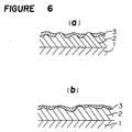
- the electricity collector of the electric conductive frit paste is formed to have a surface roughness having the maximum height more than the thickness of the anti-reflective multi-layered film, in particular, more than 0.5 ⁇ m. Accordingly, even though the anti-reflective multi-layered film (usually having a thickness of about 2,000 ⁇ - 3,000 ⁇ ) is formed on the electricity collector, a plurality of projections in the uneven surface of the electricity collector penetrate the anti-reflective multi-layered film and project from the surface of the anti-reflective multi-layered film as shown in Figure 6(a), or a plurality of projections in the uneven surface of the electricity collector come near the surface of the anti-reflective multi-layered film as shown in Figure 6(b), whereby it is possible to form the lead terminal for earth having a sufficiently low resistance.
- surface roughness and “maximum height” mean the surface roughness and the maximum height (Rmax) described in Japanese Industrial Standard JIS B 0601-1982 "Definitions and Designation of Surface Roughness".
- the panel as described above is attached to a cathode ray tube with a ultraviolet-curing resin and the electricity collector is formed to have a shape, for instance, the shape as shown in Figure 5 by the proposed electric conductive frit paste
- the electric collector absorbs and reflects ultraviolet rays to form partially a shadow, and the shadow portion produces a non-cured portion because the ultraviolet rays are not irradiated to the ultraviolet-curing resin.
- a panel with an anti-reflective film which eliminates a danger of producing a non-cured portion in the ultraviolet-curing resin, provides a sufficient antistatic effect and has an excellent geometric shape.
- a panel with an anti-reflective multi-layered film having antistatic effect wherein the electricity collector has a ultraviolet ray transmitting portion.
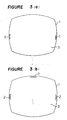
- Figure 3 is a plane view of an embodiment of the panel with an anti-reflective multi-layered film having antistatic effect of the present invention.
- a numeral 1 designates a glass substrate
- a numeral 2 designates an electricity collector formed by an electric conductive frit paste.
- An anti-reflective film 3 is formed on the entire surface of the glass substrate with the electricity collector 2.
- Figure 3a shows a panel in which two electricity collectors 2 are formed
- Figure 3b shows a panel in which three electricity collectors 2 are formed.
- the position and the number of the electricity collectors 2 are not particularly limited.
- FIG 4 are respectively plane views showing the shape of the electricity collectors according to the present invention.
- the collectors 2 as shown in Figure 4 are featurized by having ultraviolet ray transmitting portions T. It is desirable that the electricity collector has a plurality of slit-shaped ultraviolet ray transmitting portions S.
- the shapes as shown in Figures 4a and 4b are exemplified, however, the shape of the electricity collector is not limited to those and it is sufficient that it has a ultraviolet ray transmitting portion.
- An electric conductive frit paste having a composition of 10 weight % of an organic binder, 81 weight % of Ag, 6.6 weight % of PbO, 1.2 weight % of B2O3, 0.6 weight % of SiO2, and 0.6 weight % of Al2O3 was applied to two spots (as shown in Figure 3a) in the peripheral portion on a glass substrate 1 (450 mm x 350 mm) by screen-printing to thereby form a shape as shown in Figure 5.
- the frit paste was dried at 100°C for 5 minutes, and then it was baked in a heating furnace at 700°C for 4 minutes to form collectors 2 of electric conductive frit.
- the glass substrate 1 was placed on a bending mold and heated so that the glass substrate was bent by the action of dead weight wherein the surface on which the electricity collectors are formed constituted a convex surface. Then, the glass substrate was quenched for strengthening. Then, the electricity collectors were masked, and an anti-reflective multi-layered film having the construction of 1st layer 2nd layer 3rd layer 4th layer Glass ITO MgF2 ZrO2 + TiO2 MgF2 Thickness: 170 ⁇ 260 ⁇ 1200 ⁇ 900 ⁇ was formed on the convex surface of the glass substrate 1 by successively conducting vacuum deposition methods so that the anti-reflective multi-layered film was formed on the substrate except the electricity collectors 2 as shown in Figures 1(4)(b). Thus, a panel with an anti-reflective multi-layered film having antistatic effect of the present invention (sample A) was prepared.
- Lead terminals for earth was formed on the electricity collectors 2 of the sample A by using ordinary solder, and the resistance between the electric conductive layer (ITO layer) in the anti-reflective multi-layered film 3 and the lead terminal for earth was measured. As a result, the resistance was about 0.5 ⁇ .
- the panel prepared was attached to the front surface of a cathode ray tube 15 with an adhesive 16 as shown in Figure 2 to thereby form a display device.
- the lead terminal for earth was connected to the ground by a lead wire 13, and 10,000 times of ON-OFF operations of the switch of the cathode ray tube were repeated. The problem of electric breakdown did not occur at all, and there was no electric shock to a finger when touched the surface of the panel.
- a glass substrate with electricity collectors formed by baking the electric conductive frit paste was prepared in the same manner as Example 1.
- the surface of the electricity collectors had a surface roughness wherein the maximum height was about 0.5 ⁇ m.
- An anti-reflective multi-layered film was formed on the entire surface of the glass substrate in the same manner as in Example 1 to form a panel as shown in Figure 1(4)(a).
- the panel with an anti-reflective multi-layered film having antistatic effect (sample B) was prepared.
- Humidity resistance tests as described in MIL-C-675 were conducted on the sample B in the same manner as in Example. As a result, there was no change in the anti-reflective multi-layered film and the electricity collectors after the tests, and there was no deterioration of them in comparison with the state before the tests.
- a plate spring was brought into contact with the outermost layer (MgF2 layer) of the anti-reflective multi-layered film and the upper portion of an electricity collector to form a lead terminal for earth, and the resistance between the conductive layer (ITO layer) in the anti-reflective multi-layered film and the lead terminal for earth (plate spring) was measured.
- the resistance was about 1 ⁇ .
- the panel was attached to the front surface of a cathode ray tube with an adhesive in the same manner as in Example 1 to form a display device.
- the lead terminal for earth was grounded by a lead wire, and 10,000 times of ON-OFF operations of the switch of the cathode ray tube were repeated. A problem of electric breakdown did not occur at all, and there was no electric shock to a finger when touched the surface of the panel.
- An electric conductive frit paste having a composition of 10 weight % of an organic binder, 81 weight % of Ag, 6.6 weight % of PbO, 1.2 weight % of B2O3, 0.6 weight % of SiO2 and 0.6 weight % of Al2O3 was applied to two spots in a form as shown in Figure 4a on the circumference of a surface of a glass substrate 1 (450 mm x 350 mm) by using a roll coater.
- the glass substrate with the frit paste was dried at 100°C for 5 minutes, and it was baked in a heating furnace at 700°C for 4 minutes to thereby form electric collectors 2 of the electric conductive frit as shown in Figure 3a.
- the glass substrate was placed on a bending mold when it was heated, whereby it was bent by the action of dead weight so that the surface on which the electricity collectors were formed constituted a convex surface. Then, the glass substrate was rapidly quenched for strengthening.
- An anti-reflective multi-layered film having a construction of 1st layer 2nd layer 3rd layer Glass ITO ZrO2 MgF2 Optical thickness: ⁇ /4 ⁇ /2 ⁇ /4 ( ⁇ 550 nm) was formed sequentially by vacuum deposition methods so as to have the above-mentioned optical thickness while the electricity collectors were masked on the convex surface of the glass substrate 1.
- a panel with an anti-reflective multi-layered film having antistatic effect (sample C) was prepared wherein the anti-reflective multi-layered film was formed on the glass substrate except the electricity collectors 2 as shown in Figure 1(4)(b).
- a lead terminal for earth was formed on an electricity collector of sample C by using ordinary solder 14, and the resistance between the electric conductive layer (ITO layer) in the anti-reflective multi-layered film and the lead terminal for earth was measured.
- the resistance was about 0.5 ⁇ .
- the panel of sample C was attached to the front surface of a cathode ray tube 15 with an adhesive 16 of a ultraviolet-curing resin as shown in Figure 2, followed by curing the resin by irradiating ultraviolet rays. In this case, there was not found any non-cured portion of the ultraviolet-curing resin on a display device.
- the lead terminal for earth was grounded by a lead wire 13, and 10,000 times of ON-OFF operations of the switch of the cathode ray tube were repeated. As a result, there was no problem of electric breakdown and no electric shock was felt on a finger when touched the surface of the panel.
- Three electricity collectors (having a shape as shown in Figure 4b) were formed on a glass substrate as shown in Figure 3b by baking the electric conductive frit paste in the same manner as in Example 3.
- the surface of each of the electricity collectors has a surface roughness having the maximum height of about 1 ⁇ m.
- the same anti-reflective multi-layered film as in Example 3 was formed on the entire surface of the glass substrate as shown in Figure 1(4)(a), whereby a panel with the anti-reflective multi-layered film having antistatic effect was prepared (it is referred to as sample D).
- a plate spring was brought to contact with on the outermost layer of the anti-reflective multi-layered film (MgF2 layer) and above an electricity collector of sample B to thereby form a lead terminal for earth, and the resistance between the electric conductive layer (ITO layer) of the anti-reflective multi-layered film and the lead terminal for earth (plate spring) was measured.
- the resistance was about 1 ⁇ .
- the panel was attached to the front surface of a cathode ray tube with an adhesive 16 of a ultraviolet-curing resin to form a display device in the same manner as in Example 3. In this case also, there was not found any non-cured portion in the ultraviolet-curing resin.
- the lead terminal for earth was grounded by a lead wire, and 10,000 times of ON-OFF operations of the switch of the cathode ray tube were repeated. As a result, there was no problem such as electric breakdown, and there was no electrical shock on a finger when touched the surface of the panel.
- An anti-reflective multi-layered film was formed on a surface of a glass substrate which is same as in Example 1 except forming any electricity collector (it is referred to as sample E).
- a plate spring was brought to contact with a point of the circumference of the outermost layer (MgF2 layer) of the anti-reflective multi-layered film of sample E to form a lead terminal for earth, and the resistance between the electric conductive layer (ITO layer) in the anti-reflective multi-layered film and the lead terminal for earth was measured.
- the resistance in the order of 108 ⁇ .
- the panel thus formed was attached to the front surface of a cathode ray tube in the same manner as in Examples 1 and 2.
- the lead terminal for earth was grounded by a lead wire, and 10,000 times of ON-OFF operations of the switch of the cathode ray tube were repeated. As a result, there took place electric breakdown near the plate spring and the anti-reflective multi-layered film was greatly deteriorated.
- a panel with an anti-reflective multi-layered film having antistatic effect in which static electricity on the glass substrate can be led through the electric conductive layer of the anti-reflective multi-layered film to the ground at sufficiently low resistance, and which does not cause electric breakdown and deterioration of the anti-reflective multi-layered film, can be provided.
- the present invention is applicable to any type of anti-reflective multi-layered film. Namely, static electricity can be passed to the ground at sufficient low resistance by providing the electricity collectors formed by baking the electric conductive frit paste even when the electric conductive layer is formed at the nearest layer to the glass substrate, or the electric conductive layer is formed at the second layer or the layer remote from the second layer with respect to the glass substrate.
- the electricity collectors are formed by baking the electric conductive frit paste on the glass substrate at a high temperature, the electricity collectors are closely contacted to the glass substrate at a high bonding strength. Further, it has excellent humidity resistance property, is chemically and mechanically stable as is clear from Examples, and has wide practical applications.
- the panel of the present invention can be effectively produced.
- the electricity collectors are previously formed before the anti-reflective multi-layered film is formed. Accordingly, it is possible to supply the panel prepared in accordance with the present invention in a stable manner without damaging the film after the anti-reflective multi-layered film has been formed.
- the ultraviolet ray transmitting portion in the electricity collector in the panel with the anti-reflective multi-layered film having antistatic effect, there is provided a panel with an anti-reflective multi-layered film having antistatic effect which does not produce a non-cured portion in the ultraviolet-curing resin even when the panel is attached to a cathode ray tube with such resin.
Abstract
Description
- The present invention relates to a panel with an anti-reflective multi-layered film thereon.
- Various types of an anti-reflective film consisting of a single or a plurality of layers have been proposed wherein the film is coated on the front surface of a display device such as a cathode ray tube or on a panel to be disposed in front of the display device in order to eliminate the difficulty that the display portion is hardly seen due to an image by the reflection of an external light, and to reduce a degree of reflection.
- As the anti-reflective film, there have been proposed a single layered anti-reflective film wherein a material having a low refractive index is used to form a layer having an optical thickness of λ/4 of a wave length which causes reflection, a two-layered anti-reflective film wherein two layers of a low refractive index layer and a high refractive index layer are coated to have respective optical thickness of λ/4 and λ/2 when viewed from the side of air, a three-layered anti-reflective film wherein three layers of a low refractive index layer, a high refractive index layer and an intermediate refractive index layer are coated to have respective optical thickness of λ/4, λ/2 and λ/4 when viewed from the side of air, and a four anti-reflective film wherein four layers of a low refractive index layer, a high refractive index layer, an intermediate refractive index layer and a low refractive index layer to have respective optical thickness of λ/4, λ/2, λ/4 and λ/4 when viewed from the side of air.
- On the other hand, glass or a plastic material used for a cathode ray tube or a front panel has no electric conducting property, and the surface of the cathode ray tube is electrified by an amount of static electricity produced during the operation of the cathode ray tube. The static electricity causes an electric discharge to a human body or is apt to attract dust. This causes a great problem in a terminal of a computer, a display device for a word processor, and so on.
- Accordingly, there has been studied to propose an anti-reflective film having electric conductive property, namely, an anti-reflective film wherein at least one layer is composed of a transparent material having electric conductive property. There has been known as a transparent conductive film, ITO (tin-doped indium oxide), SnO₂ (tin oxide) and so on. However, these materials have a high refractive index (for instance, ITO has a refractive index of about 2.0 and SnO₂ has 1.90), and therefore the construction of film for the anti-reflective film is limited. Namely, since the transparent electric conductive layer has a high refractive index, it does not function as a single-layered anti-reflective film and rather, it enhances reflectivity. Further, in a case of an anti-reflective multi-layered film, it is necessary to form a film having a low refractive index for the outermost layer facing the side of air as is clear from the construction of the above-mentioned anti-reflective film. Since there is no material for the transparent conductive film which satisfies the property of a low refractive index as required, it is necessary that a transparent conductive film is used for an inner layer and an insulating material having a low refractive index such a MgF₂, SiO₂ or the like is used for the outermost layer.
- Various methods have been proposed to produce a panel with an anti-reflective multi-layered film wherein an electric charge produced on the surface of the panel by the electrification is led to the ground through a transparent conductive film which is formed as an inner layer in the anti-reflective-multi-layered film.
- An attempt to let an electric charge escape by forming a solder layer on the outermost layer of the anti-reflective film was made. As a result, it was found that the wettability of the outermost layer, e.g. MgF₂ or SiO₂ of the anti-reflective film to the solder layer was not so good, and provision of the solder layer on the outermost layer did not sufficiently function as earthing at a low resistance value because a non-conductive layer was interposed.
- An attempt of letting an electric charge escape by directly contacting a plate spring made of metal on the outermost layer of the anti-reflective film was made. However, the resistance between the plate spring and the transparent conductive layer was very high because the outermost layer without electric conductive property was intervened and a complete contacting state of the plate spring could not be obtained, whereby an electric breakdown was caused at a part of the anti-reflective multi-layered film to thereby deteriorate the film.
- Further, an attempt of bonding an electric conductive tape comprising a copper foil with an adhesive to the surface of the multi-layered film was made. However, the electric conductivity of the adhesive was not sufficient and an electric breakdown was caused.
- It is an object of the present invention to eliminate the above-mentioned problems and to provide a panel with an anti-reflective multi layered film thereon which comprises a glass substrate, an electricity collector for leading static electricity which is formed by baking an electric conductive frit paste on the glass substrate, and has a rough surface, an anti-reflective multi-layered film formed on said glass substrate so as to cover at least a portion of the electricity collector and including an inner electric conductive layer to provide antistatic effect, wherein the thickness of said anti-reflective multi-layered film is less than the maximum height of the surface roughness of said electricity collector, and a lead terminal for earth provided on the outermost layer of the anti-reflective film and above the electricity collector, whereby static electricity produced on the glass substrate with the anti-reflective multi-layered film is collected at the electricity collector through the electric conductive layer so that the static electricity is led to the outside through the lead terminal for earth via the electricity collector.
- In the accompanying drawings:
- Figure 1 is a diagram showing an embodiment of the process of preparing a panel with an anti-reflective multi-layered film thereon having antistatic effect according to the present invention;
- Figure 2 is a longitudinal cross-sectional view of a display device with a panel prepared by an embodiment of the present invention;
- Figure 3 is a plane view -of an embodiment of the panel with an anti-reflective multi-layered film having antistatic effect of the present invention;
- Figure 4 is plane views showing embodiments of an electricity collector used for the panel with an anti- reflective multi-layered film having antistatic effect of the present invention;
- Figure 5 is a plane view showing another embodiment of the electricity collector of the present invention; and
- Figure 6 is an enlarged cross-sectional view showing a part of the electricity collector of the panel shown in Figure 1(5)(a).
- Embodiments of the process for producing a panel with an anti-reflective multi-layered film having antistatic effect of the present invention will be described with reference to the drawings.
- In Figure 1, a
reference numeral 1 designates a glass substrate, anumeral 2 designates an electricity collector formed by an electric conductive frit paste, anumeral 3 designates an anti-reflective multi-layered film having an inner conductive layer and having antistatic effect, anumeral 4 designates a lead terminal for earth, and anumeral 5 designates a panel with an anti-reflective multi-layered film having antistatic effect of the present invention. - As shown in Figure 1(1), an electric conductive
frit paste 2 is screen-printed or coated by using a roll coater or a meniscus coater or the like at a portion near the periphery of a surface of theglass substrate 1 after theglass substrate 1 has been cleaned. The electric conductivefrit paste 2 may be formed in a dotted form or in a linear form having a length. Further, it may be formed at plural spots on theglass substrate 1. - Then, the electric conductive
frit paste 2 is provisionally dried by heating it at about 80°C - 120°C, and it is baked at the inherent baking temperature to thereby bond thepaste 2 on the glass substrate. - As the electric conductive
frit paste 2 used in the present invention, it is preferable to use such material that powder of a metal having excellent electric conductivity such as silver, aluminum, gold, copper, platinum, palladium or the like is mixed with glass frit having a low melting point (for instance, PbO-B₂O₃ series glass frit, PbO-B₂O₃-SiO₂ series glass frit, or PbO-ZnO-B₂O₃ series glass frit), and an organic solvent, a thickening agent and an additive or additives are added to the mixture, if necessary, to obtain a paste of mixture. It is necessary for the electric conductive frit paste to have a range of baking temperature wherein the paste can be bonded to the glass substrate at a temperature range sufficient to bending glass (580°C - 640°C) or strengthening the glass substrate (610°C - 680°C). With use of the above-mentioned glass frit, a panel having a curved surface, for instance, a panel which is capable of attaching to the front surface of a cathode ray tube or a strengthened panel can be prepared at the same time of baking the electric conductive glass frit 2. Figure 1(2) shows a case that theglass substrate 1 is subjected to a predetermined bending operation at the same time of the baking of the electric conductivefrit paste 2. - A baking temperature for the electric conductive
frit paste 2 is determined depending on a composition of thepaste 2. The baking temperature is substantially same or very close to the softening temperature of glass. Accordingly, when a panel having a predetermined curved surface, for instance, a curved surface which is capable of attaching to the front surface of a cathode ray tube is prepared, the glass substrate is bend-shaped before, after or at the same time of the baking of the electric conductivefrit paste 2. Figure 1(2) shows a case that a bend-shaping operation is applied to theglass substrate 1. - In the next place, the anti-reflective
multi-layered film 3 having antistatic effect is formed on the glass substrate on which the electric conductivefrit paste 2 is formed by baking. When thefilm 3 is to be formed, it may be formed to cover a part or its entirety of theelectricity collector 2 made of the electric conductive frit paste as shown in Figure 1(3)(a). Or, thefilm 3 may be formed on theglass substrate 1 except theelectricity collector 2 by method of, for instance, masking theelectricity collector 2 so that thefilm 3 is in contact with theelectricity collector 2 as shown in Figure 1(3)(b). - It is obliged to form the outermost layer of the anti-reflective film by an insulating material having a low refractive index as described above. As a material for the outermost layer, it is sufficient to use a material having a low refractive index such as MgF₂, SiO₂, CaF₂, cryolite or the like. In particular, MgF₂ or SiO₂ is preferably used from the viewpoint that it is chemically and physically durable, allows a large scale production, and is easily available. Further, SiO₂ including a small amount of Zr, Hf, Ti, In, Ta or Sn or the like to further improve acid resistance, for instance, SiTixOy, SiZrxOy or the like can be used.
- Finally, the lead terminal for
earth 4 is provided on the outermost layer of theanti-reflective film 3 and above theelectricity collector 2 as shown in Figure 1(4)(a), or it is attached to theelectricity collector 2 as shown in Figure 1(4)(b). Thus, thepanel 5 with an anti-reflective multi-layered film having antistatic effect is prepared. The lead terminal forearth 4 may be formed by solder, or by attaching a plate spring. Or, a plate spring may be sandwiched when the panel with an anti-reflective multi-layered film is fitted to a framework of display or television. - In the
panel 5 with an anti-reflective multi-layered film having antistatic effect prepared as described above, it is so adapted that static electricity produced on the glass substrate on which the anti-reflective multi-layered film is formed is collected to theelectricity collector 2 through an electric conductive layer in the film and it is led to the outside through the lead terminal forearth 4. - In a case that the panel as shown in Figure 1(4)(b) is modified to be a panel as shown in Figure 1(5)(b), an end portion of an electric conductive layer in the anti-reflective
multi-layered film 3 having antistatic effect and theelectricity collector 2, and theelectricity collector 2 and the lead terminal forearth 4 are respectively in direct contact with each other even though the electric conductive layer is formed at any number of layer from the glass plate in the anti-reflectivemulti-layered film 3. Accordingly, the resistance between the electric conductive layer in the anti-reflectivemulti-layered film 3 and the lead terminal forearth 4 is very low as about 0.5 Ω - 3 Ω, so that it is easy to lead the static electricity to the ground. - In a case that the panel as shown in Figure 1(4)(a) is modified to be a panel as shown in Figure 1(5)(a), the electric conductive layer in the anti-reflective
multi-layered film 3 and theelectricity collector 2, and theelectricity collector 2 and the lead terminal forearth 4 are respectively do not directly contact with each other, and static electricity is led through the insulating layer, whereby the resistance between the electric conductive layer in the anti-reflectivemulti-layered film 3 and the lead terminal forearth 4 becomes relatively high in comparison with the above-mentioned case wherein the panel as shown in Figure 1(4)(b) is used. - However, in the present invention, the electricity collector of the electric conductive frit paste is formed to have a surface roughness having the maximum height more than the thickness of the anti-reflective multi-layered film, in particular, more than 0.5 µm. Accordingly, even though the anti-reflective multi-layered film (usually having a thickness of about 2,000 Å - 3,000 Å) is formed on the electricity collector, a plurality of projections in the uneven surface of the electricity collector penetrate the anti-reflective multi-layered film and project from the surface of the anti-reflective multi-layered film as shown in Figure 6(a), or a plurality of projections in the uneven surface of the electricity collector come near the surface of the anti-reflective multi-layered film as shown in Figure 6(b), whereby it is possible to form the lead terminal for earth having a sufficiently low resistance.
- In the description of the present invention, "surface roughness" and "maximum height" mean the surface roughness and the maximum height (Rmax) described in Japanese Industrial Standard JIS B 0601-1982 "Definitions and Designation of Surface Roughness".
- In a case that the panel as described above is attached to a cathode ray tube with a ultraviolet-curing resin and the electricity collector is formed to have a shape, for instance, the shape as shown in Figure 5 by the proposed electric conductive frit paste, there is a possibility that the electric collector absorbs and reflects ultraviolet rays to form partially a shadow, and the shadow portion produces a non-cured portion because the ultraviolet rays are not irradiated to the ultraviolet-curing resin. As another embodiment of the present invention, there is provided a panel with an anti-reflective film which eliminates a danger of producing a non-cured portion in the ultraviolet-curing resin, provides a sufficient antistatic effect and has an excellent geometric shape. Namely, there is provided a panel with an anti-reflective multi-layered film having antistatic effect wherein the electricity collector has a ultraviolet ray transmitting portion.
- Figure 3 is a plane view of an embodiment of the panel with an anti-reflective multi-layered film having antistatic effect of the present invention. In Figure 3, a
numeral 1 designates a glass substrate, and anumeral 2 designates an electricity collector formed by an electric conductive frit paste. Ananti-reflective film 3 is formed on the entire surface of the glass substrate with theelectricity collector 2. - Figure 3a shows a panel in which two
electricity collectors 2 are formed, and Figure 3b shows a panel in which threeelectricity collectors 2 are formed. In the present invention, however, the position and the number of theelectricity collectors 2 are not particularly limited. - Figure 4 are respectively plane views showing the shape of the electricity collectors according to the present invention. The
collectors 2 as shown in Figure 4 are featurized by having ultraviolet ray transmitting portions T. It is desirable that the electricity collector has a plurality of slit-shaped ultraviolet ray transmitting portions S. The shapes as shown in Figures 4a and 4b are exemplified, however, the shape of the electricity collector is not limited to those and it is sufficient that it has a ultraviolet ray transmitting portion. - Now, the present invention will be described in detail with reference to Examples. However, it should be understood that the present invention is by no means restricted to such specific Examples.
- An electric conductive frit paste having a composition of 10 weight % of an organic binder, 81 weight % of Ag, 6.6 weight % of PbO, 1.2 weight % of B₂O₃, 0.6 weight % of SiO₂, and 0.6 weight % of Al₂O₃ was applied to two spots (as shown in Figure 3a) in the peripheral portion on a glass substrate 1 (450 mm x 350 mm) by screen-printing to thereby form a shape as shown in Figure 5. The frit paste was dried at 100°C for 5 minutes, and then it was baked in a heating furnace at 700°C for 4 minutes to form
collectors 2 of electric conductive frit. Theglass substrate 1 was placed on a bending mold and heated so that the glass substrate was bent by the action of dead weight wherein the surface on which the electricity collectors are formed constituted a convex surface. Then, the glass substrate was quenched for strengthening. Then, the electricity collectors were masked, and an anti-reflective multi-layered film having the construction of1st layer 2nd layer 3rd layer 4th layer Glass ITO MgF₂ ZrO₂ + TiO₂ MgF₂ Thickness: 170 Å 260 Å 1200 Å 900Å glass substrate 1 by successively conducting vacuum deposition methods so that the anti-reflective multi-layered film was formed on the substrate except theelectricity collectors 2 as shown in Figures 1(4)(b). Thus, a panel with an anti-reflective multi-layered film having antistatic effect of the present invention (sample A) was prepared. - In heat tests (the sample A was kept at -40°C and 150°C for 4 hours respectively) and dissolving tests (it was immersed in 50% of CH₃COOH aq for 24 hours and 10% of NaCl aq for 24 hours), there was no change of anti-reflective multi-layered film and the electricity collectors.
- Further, abrasion resistance tests by reciplocating 20 times with an eraser and bonding tests with an adhesive tape were carried out for the anti-reflective multi-layered film and the electricity collectors of the sample A. In these tests, no change was found.
- Lead terminals for earth was formed on the
electricity collectors 2 of the sample A by using ordinary solder, and the resistance between the electric conductive layer (ITO layer) in the anti-reflectivemulti-layered film 3 and the lead terminal for earth was measured. As a result, the resistance was about 0.5 Ω. - The panel prepared was attached to the front surface of a
cathode ray tube 15 with an adhesive 16 as shown in Figure 2 to thereby form a display device. The lead terminal for earth was connected to the ground by alead wire 13, and 10,000 times of ON-OFF operations of the switch of the cathode ray tube were repeated. The problem of electric breakdown did not occur at all, and there was no electric shock to a finger when touched the surface of the panel. - A glass substrate with electricity collectors formed by baking the electric conductive frit paste was prepared in the same manner as Example 1. The surface of the electricity collectors had a surface roughness wherein the maximum height was about 0.5 µm. An anti-reflective multi-layered film was formed on the entire surface of the glass substrate in the same manner as in Example 1 to form a panel as shown in Figure 1(4)(a). Thus, the panel with an anti-reflective multi-layered film having antistatic effect (sample B) was prepared.
- Humidity resistance tests as described in MIL-C-675 were conducted on the sample B in the same manner as in Example. As a result, there was no change in the anti-reflective multi-layered film and the electricity collectors after the tests, and there was no deterioration of them in comparison with the state before the tests.
- Further, tests on the heat resistance property, the dissolving property, the abrasion resistance property and the bonding property were conducted in the same manner as in Example 1. No change was found.
- A plate spring was brought into contact with the outermost layer (MgF₂ layer) of the anti-reflective multi-layered film and the upper portion of an electricity collector to form a lead terminal for earth, and the resistance between the conductive layer (ITO layer) in the anti-reflective multi-layered film and the lead terminal for earth (plate spring) was measured. The resistance was about 1 Ω.
- The panel was attached to the front surface of a cathode ray tube with an adhesive in the same manner as in Example 1 to form a display device. The lead terminal for earth was grounded by a lead wire, and 10,000 times of ON-OFF operations of the switch of the cathode ray tube were repeated. A problem of electric breakdown did not occur at all, and there was no electric shock to a finger when touched the surface of the panel.
- An electric conductive frit paste having a composition of 10 weight % of an organic binder, 81 weight % of Ag, 6.6 weight % of PbO, 1.2 weight % of B₂O₃, 0.6 weight % of SiO₂ and 0.6 weight % of Al₂O₃ was applied to two spots in a form as shown in Figure 4a on the circumference of a surface of a glass substrate 1 (450 mm x 350 mm) by using a roll coater. The glass substrate with the frit paste was dried at 100°C for 5 minutes, and it was baked in a heating furnace at 700°C for 4 minutes to thereby form
electric collectors 2 of the electric conductive frit as shown in Figure 3a. The glass substrate was placed on a bending mold when it was heated, whereby it was bent by the action of dead weight so that the surface on which the electricity collectors were formed constituted a convex surface. Then, the glass substrate was rapidly quenched for strengthening. An anti-reflective multi-layered film having a construction of1st layer 2nd layer 3rd layer Glass ITO ZrO₂ MgF₂ Optical thickness: λ/4 λ/2 λ/4 (λ = 550 nm) glass substrate 1. Thus, a panel with an anti-reflective multi-layered film having antistatic effect (sample C) was prepared wherein the anti-reflective multi-layered film was formed on the glass substrate except theelectricity collectors 2 as shown in Figure 1(4)(b). - Heat resistance tests (it was heated at -40°C and 150°C for 4 hours respectively) and dissolving tests (it was immersed in 50% of CH₃COOH aq for 24 hours and in 10% of NaCl aq for 24 hours) were respectively conducted. As a result, no change was found in the anti-reflective multi-layered film and the electricity collectors.
- Further, abrasion resistance tests by reciplocating times by using an eraser and bonding tests by using an adhesive tape were conducted on the anti-reflective multi-layered film and the electricity collectors of sample C. As a result, no change was found.
- A lead terminal for earth was formed on an electricity collector of sample C by using
ordinary solder 14, and the resistance between the electric conductive layer (ITO layer) in the anti-reflective multi-layered film and the lead terminal for earth was measured. The resistance was about 0.5 Ω. - The panel of sample C was attached to the front surface of a
cathode ray tube 15 with an adhesive 16 of a ultraviolet-curing resin as shown in Figure 2, followed by curing the resin by irradiating ultraviolet rays. In this case, there was not found any non-cured portion of the ultraviolet-curing resin on a display device. - The lead terminal for earth was grounded by a
lead wire 13, and 10,000 times of ON-OFF operations of the switch of the cathode ray tube were repeated. As a result, there was no problem of electric breakdown and no electric shock was felt on a finger when touched the surface of the panel. - Three electricity collectors (having a shape as shown in Figure 4b) were formed on a glass substrate as shown in Figure 3b by baking the electric conductive frit paste in the same manner as in Example 3. The surface of each of the electricity collectors has a surface roughness having the maximum height of about 1 µm. Then, the same anti-reflective multi-layered film as in Example 3 was formed on the entire surface of the glass substrate as shown in Figure 1(4)(a), whereby a panel with the anti-reflective multi-layered film having antistatic effect was prepared (it is referred to as sample D).
- Humidity resistance tests described in MIL-C-675A were conducted on sample D in the same manner as in Example 3. As a result, there was no change in the anti-reflective multi-layered film and the electricity collectors after the tests, and there was no deterioration.
- Various tests on the heat resistance property, the dissolving property, the abrasion resistance property and the bonding property were conducted in the same manner as in Example 3. However, there was no change.
- A plate spring was brought to contact with on the outermost layer of the anti-reflective multi-layered film (MgF₂ layer) and above an electricity collector of sample B to thereby form a lead terminal for earth, and the resistance between the electric conductive layer (ITO layer) of the anti-reflective multi-layered film and the lead terminal for earth (plate spring) was measured. The resistance was about 1 Ω.
- The panel was attached to the front surface of a cathode ray tube with an adhesive 16 of a ultraviolet-curing resin to form a display device in the same manner as in Example 3. In this case also, there was not found any non-cured portion in the ultraviolet-curing resin.
- The lead terminal for earth was grounded by a lead wire, and 10,000 times of ON-OFF operations of the switch of the cathode ray tube were repeated. As a result, there was no problem such as electric breakdown, and there was no electrical shock on a finger when touched the surface of the panel.
- An anti-reflective multi-layered film was formed on a surface of a glass substrate which is same as in Example 1 except forming any electricity collector (it is referred to as sample E).
- A plate spring was brought to contact with a point of the circumference of the outermost layer (MgF₂ layer) of the anti-reflective multi-layered film of sample E to form a lead terminal for earth, and the resistance between the electric conductive layer (ITO layer) in the anti-reflective multi-layered film and the lead terminal for earth was measured. The resistance in the order of 10⁸ Ω.
- The panel thus formed was attached to the front surface of a cathode ray tube in the same manner as in Examples 1 and 2. The lead terminal for earth was grounded by a lead wire, and 10,000 times of ON-OFF operations of the switch of the cathode ray tube were repeated. As a result, there took place electric breakdown near the plate spring and the anti-reflective multi-layered film was greatly deteriorated.
- In accordance with the present invention, a panel with an anti-reflective multi-layered film having antistatic effect in which static electricity on the glass substrate can be led through the electric conductive layer of the anti-reflective multi-layered film to the ground at sufficiently low resistance, and which does not cause electric breakdown and deterioration of the anti-reflective multi-layered film, can be provided.
- The present invention is applicable to any type of anti-reflective multi-layered film. Namely, static electricity can be passed to the ground at sufficient low resistance by providing the electricity collectors formed by baking the electric conductive frit paste even when the electric conductive layer is formed at the nearest layer to the glass substrate, or the electric conductive layer is formed at the second layer or the layer remote from the second layer with respect to the glass substrate.
- In the present invention, since the electricity collectors are formed by baking the electric conductive frit paste on the glass substrate at a high temperature, the electricity collectors are closely contacted to the glass substrate at a high bonding strength. Further, it has excellent humidity resistance property, is chemically and mechanically stable as is clear from Examples, and has wide practical applications.
- Further, in the present invention, since the electricity collectors can be formed by baking at the same time of bending and/or strengthening operations of the glass substrate, the panel of the present invention can be effectively produced. The electricity collectors are previously formed before the anti-reflective multi-layered film is formed. Accordingly, it is possible to supply the panel prepared in accordance with the present invention in a stable manner without damaging the film after the anti-reflective multi-layered film has been formed.
- Further, by forming the ultraviolet ray transmitting portion in the electricity collector in the panel with the anti-reflective multi-layered film having antistatic effect, there is provided a panel with an anti-reflective multi-layered film having antistatic effect which does not produce a non-cured portion in the ultraviolet-curing resin even when the panel is attached to a cathode ray tube with such resin.
Claims (11)
a glass substrate,
an electricity collector for leading static electricity which is formed by baking an electric conductive frit paste on the glass substrate, and which has a rough surface, an anti-reflective multi-layered film formed on said glass substrate so as to cover at least a portion of the electricity collector and including an inner electric conductive layer to provide antistatic effect, wherein the thickness of said anti-reflective multi-layered film is less than the maximum height of the surface roughness of said electricity collector, and
a lead terminal for earth provided on the outermost layer of the anti-reflective film and above the electricity collector, whereby static electricity produced on the glass substrate with the anti-reflective multi-layered film is collected at the electricity collector through the electric conductive layer so that the static electricity is led to the outside through the lead terminal for earth via the electricity collector.
a glass substrate,
an electricity collector for leading static electricity which is formed by baking an electric conductive frit paste on the glass substrate,
an anti-reflective multi-layered film formed on the glass substrate except the electricity collector, which has an inner electric conductive layer to provide antistatic effect, and
a lead terminal for earth formed on the electricity collector, whereby static electricity produced on the glass substrate with the anti-reflective multi-layered film is collected at the electricity collector through the electric conductive layer so that the static electricity is led to the outside through the lead terminal for each via the electricity collector.
a ultraviolet-curing resin layer formed on the front surface of the cathode ray tube main body, and
a panel with an anti-reflective multi-layered film which has antistatic effect defined in any one of Claims 1 to 6, and has a surface without an anti-reflective multi-layered film thereon, which is attached to the ultraviolet-curing resin layer.
forming an electricity collector for leading static electricity having a surface roughness having the maximum height more than the thickness of an anti-reflective multi-layered film to be formed, on a glass substrate by printing, or coating an electric conductive frit paste, followed by drying and baking the paste,
forming the anti-reflective multi-layered film having an inner electric conductive layer and having antistatic effect on the glass substrate with the electricity collector so as to cover at least a part of the electricity collector, and
forming a lead terminal for earth on the outermost layer of the anti-reflective multi-layered film and above the electricity collector.
forming an electricity collector for leading static electricity by printing or coating an electric conductive frit paste on a glass plate, followed by drying and baking the paste,
forming an anti-reflective multi-layered film having an inner electric conductive layer and having antistatic effect on the glass plate except the electricity collector so that the anti-reflective multi-layered film is in contact with the electricity collector, and
forming a lead terminal for earth on the electricity collector.
Applications Claiming Priority (4)
| Application Number | Priority Date | Filing Date | Title |
|---|---|---|---|
| JP30681888 | 1988-12-06 | ||
| JP306818/88 | 1988-12-06 | ||
| JP7122889 | 1989-06-20 | ||
| JP71228/89U | 1989-06-20 |
Publications (3)
| Publication Number | Publication Date |
|---|---|
| EP0372488A2 true EP0372488A2 (en) | 1990-06-13 |
| EP0372488A3 EP0372488A3 (en) | 1991-09-25 |
| EP0372488B1 EP0372488B1 (en) | 1995-03-29 |
Family
ID=26412336
Family Applications (1)
| Application Number | Title | Priority Date | Filing Date |
|---|---|---|---|
| EP89122398A Expired - Lifetime EP0372488B1 (en) | 1988-12-06 | 1989-12-05 | Panel with anti-reflective multi-layered film thereon |
Country Status (4)
| Country | Link |
|---|---|
| US (1) | US5051652A (en) |
| EP (1) | EP0372488B1 (en) |
| KR (1) | KR960004588B1 (en) |
| DE (1) | DE68921964D1 (en) |
Cited By (6)
| Publication number | Priority date | Publication date | Assignee | Title |
|---|---|---|---|---|
| EP0552796A1 (en) * | 1992-01-24 | 1993-07-28 | Asahi Glass Company Ltd. | Conductive film and low reflection conductive film and processes for their production |
| EP0565026A1 (en) * | 1992-04-06 | 1993-10-13 | Matsushita Electronics Corporation | Display device and a method for producing the same |
| EP0568702A1 (en) * | 1991-11-05 | 1993-11-10 | Mitsubishi Denki Kabushiki Kaisha | Cathode-ray tube |
| EP0600551A1 (en) * | 1992-12-03 | 1994-06-08 | Koninklijke Philips Electronics N.V. | Method of manufacturing a display window for a cathode ray tube |
| CN100361325C (en) * | 2004-11-04 | 2008-01-09 | 李德杰 | LED with total antireflection film and method for making same |
| EP1280868B1 (en) * | 2000-05-12 | 2008-05-07 | 3M Innovative Properties Company | Rigid substrate lamination adhesive |
Families Citing this family (22)
| Publication number | Priority date | Publication date | Assignee | Title |
|---|---|---|---|---|
| KR940011569B1 (en) * | 1990-10-24 | 1994-12-21 | 미쯔비시덴끼 가부시끼가이샤 | Crt having low reflectivity film |
| US5660876A (en) * | 1991-06-07 | 1997-08-26 | Sony Corporation | Method of manufacturing cathode ray tube with a nonglare multi-layered film |
| JP3223261B2 (en) * | 1992-06-04 | 2001-10-29 | 三菱電機株式会社 | Cathode ray tube and method of manufacturing the same |
| US5444329A (en) * | 1992-11-06 | 1995-08-22 | Kabushiki Kaisha Toshiba | Antireflection film and display apparatus comprising the same |
| JP2981528B2 (en) * | 1992-12-25 | 1999-11-22 | 三菱電機株式会社 | Cathode ray tube and method of manufacturing the same |
| US5652477A (en) * | 1995-11-08 | 1997-07-29 | Chunghwa Picture Tubes, Ltd. | Multilayer antistatic/antireflective coating for display device |
| US5773150A (en) * | 1995-11-17 | 1998-06-30 | Chunghwa Picture Tubes, Ltd. | Polymeric antistatic coating for cathode ray tubes |
| JPH1031425A (en) * | 1996-07-17 | 1998-02-03 | Canon Inc | Projection type display device |
| JPH10186102A (en) * | 1996-12-26 | 1998-07-14 | Yazaki Corp | Anti-reflection film |
| JP3313298B2 (en) * | 1997-02-24 | 2002-08-12 | 富士通株式会社 | Plasma display panel and method of manufacturing the same |
| TW417025B (en) * | 1997-04-10 | 2001-01-01 | Sumitomo Chemical Co | Front plate for plasma display |
| KR100396367B1 (en) * | 1998-06-18 | 2003-09-02 | 후다바 덴시 고교 가부시키가이샤 | Aluminum paste for fluorescent display device, fluorescent display device using aluminum paste and method for manufacturing same |
| US6623662B2 (en) | 2001-05-23 | 2003-09-23 | Chunghwa Picture Tubes, Ltd. | Carbon black coating for CRT display screen with uniform light absorption |
| US6746530B2 (en) | 2001-08-02 | 2004-06-08 | Chunghwa Pictures Tubes, Ltd. | High contrast, moisture resistant antistatic/antireflective coating for CRT display screen |
| US6521346B1 (en) | 2001-09-27 | 2003-02-18 | Chunghwa Picture Tubes, Ltd. | Antistatic/antireflective coating for video display screen with improved refractivity |
| US6764580B2 (en) * | 2001-11-15 | 2004-07-20 | Chungwa Picture Tubes, Ltd. | Application of multi-layer antistatic/antireflective coating to video display screen by sputtering |
| US20030179455A1 (en) * | 2002-03-22 | 2003-09-25 | Jeffrey Hunt | Fingerprint resistant anti-reflection coatings for plastic substrates |
| US6656331B2 (en) | 2002-04-30 | 2003-12-02 | Chunghwa Picture Tubes, Ltd. | Application of antistatic/antireflective coating to a video display screen |
| US6590352B1 (en) | 2002-04-30 | 2003-07-08 | Chunghwa Picture Tubes, Ltd. | Electrical grounding of CRT antistatic/antireflective coating |
| KR20060059267A (en) * | 2003-10-30 | 2006-06-01 | 젠텍스 코포레이션 | Electrochromic device having a self-cleaning hydrophilic coating with an acid resistant under layer |
| JP4783301B2 (en) * | 2006-02-08 | 2011-09-28 | 株式会社ブリヂストン | Display optical filter manufacturing method, display optical filter, display including the same, and plasma display panel |
| KR20140095343A (en) | 2013-01-24 | 2014-08-01 | 삼성디스플레이 주식회사 | Flexible display |
Citations (4)
| Publication number | Priority date | Publication date | Assignee | Title |
|---|---|---|---|---|
| US3721595A (en) * | 1969-07-01 | 1973-03-20 | Ppg Industries Inc | Applying electroconductive heating circuits to glass |
| US4010304A (en) * | 1974-07-26 | 1977-03-01 | Saint-Gobain Industries | Heated windows having vacuum-deposited layers |
| EP0145201A1 (en) * | 1983-11-10 | 1985-06-19 | Optical Coating Laboratory, Inc. | Antireflection optical coating with antistatic properties |
| EP0200452A2 (en) * | 1985-04-22 | 1986-11-05 | Toray Industries, Inc. | Light-transmissible plate shielding electromagnetic waves |
Family Cites Families (2)
| Publication number | Priority date | Publication date | Assignee | Title |
|---|---|---|---|---|
| US4563612A (en) * | 1984-06-25 | 1986-01-07 | Rca Corporation | Cathode-ray tube having antistatic silicate glare-reducing coating |
| DE3629996A1 (en) * | 1986-09-03 | 1988-03-17 | Flachglas Ag | ATTACHMENT UNIT FOR THE CATHODE RAY TUBES OF MONITORS, TELEVISION DEVICES AND THE LIKE |
-
1989
- 1989-12-04 US US07/445,026 patent/US5051652A/en not_active Expired - Fee Related
- 1989-12-05 KR KR1019890017996A patent/KR960004588B1/en not_active IP Right Cessation
- 1989-12-05 DE DE68921964T patent/DE68921964D1/en not_active Expired - Lifetime
- 1989-12-05 EP EP89122398A patent/EP0372488B1/en not_active Expired - Lifetime
Patent Citations (4)
| Publication number | Priority date | Publication date | Assignee | Title |
|---|---|---|---|---|
| US3721595A (en) * | 1969-07-01 | 1973-03-20 | Ppg Industries Inc | Applying electroconductive heating circuits to glass |
| US4010304A (en) * | 1974-07-26 | 1977-03-01 | Saint-Gobain Industries | Heated windows having vacuum-deposited layers |
| EP0145201A1 (en) * | 1983-11-10 | 1985-06-19 | Optical Coating Laboratory, Inc. | Antireflection optical coating with antistatic properties |
| EP0200452A2 (en) * | 1985-04-22 | 1986-11-05 | Toray Industries, Inc. | Light-transmissible plate shielding electromagnetic waves |
Cited By (9)
| Publication number | Priority date | Publication date | Assignee | Title |
|---|---|---|---|---|
| EP0568702A1 (en) * | 1991-11-05 | 1993-11-10 | Mitsubishi Denki Kabushiki Kaisha | Cathode-ray tube |
| EP0568702A4 (en) * | 1991-11-05 | 1993-11-24 | Mitsubishi Denki Kabushiki Kaisha | Cathode-ray tube |
| EP0552796A1 (en) * | 1992-01-24 | 1993-07-28 | Asahi Glass Company Ltd. | Conductive film and low reflection conductive film and processes for their production |
| US5320913A (en) * | 1992-01-24 | 1994-06-14 | Asahi Glass Company Ltd. | Conductive film and low reflection conductive film, and processes for their production |
| EP0565026A1 (en) * | 1992-04-06 | 1993-10-13 | Matsushita Electronics Corporation | Display device and a method for producing the same |
| US5539275A (en) * | 1992-04-06 | 1996-07-23 | Matsushita Electric Corporation | Display device and a method for producing the same |
| EP0600551A1 (en) * | 1992-12-03 | 1994-06-08 | Koninklijke Philips Electronics N.V. | Method of manufacturing a display window for a cathode ray tube |
| EP1280868B1 (en) * | 2000-05-12 | 2008-05-07 | 3M Innovative Properties Company | Rigid substrate lamination adhesive |
| CN100361325C (en) * | 2004-11-04 | 2008-01-09 | 李德杰 | LED with total antireflection film and method for making same |
Also Published As
| Publication number | Publication date |
|---|---|
| EP0372488A3 (en) | 1991-09-25 |
| DE68921964D1 (en) | 1995-05-04 |
| KR900010894A (en) | 1990-07-11 |
| KR960004588B1 (en) | 1996-04-09 |
| US5051652A (en) | 1991-09-24 |
| EP0372488B1 (en) | 1995-03-29 |
Similar Documents
| Publication | Publication Date | Title |
|---|---|---|
| EP0372488B1 (en) | Panel with anti-reflective multi-layered film thereon | |
| US4412255A (en) | Transparent electromagnetic shield and method of manufacturing | |
| EP1031111B1 (en) | Touch panel | |
| US6379509B2 (en) | Process for forming electrodes | |
| US4563612A (en) | Cathode-ray tube having antistatic silicate glare-reducing coating | |
| EP1216147B1 (en) | Glazing | |
| JPH05109341A (en) | Thin film switch | |
| EP0386235B1 (en) | Panel for cathode ray tube | |
| US20020101409A1 (en) | Glass touch panel | |
| US4778732A (en) | Electrically conductive glass sheet | |
| JPS63265499A (en) | Electromagnetic shielding panel | |
| JP3592830B2 (en) | Display element substrate | |
| EP0589147B1 (en) | Cathode ray tube and method of producing the same | |
| JPH066393Y2 (en) | Panel with antireflection multilayer film having antistatic effect | |
| JP2770013B2 (en) | Electroluminescence display device | |
| JPS61176035A (en) | Plasma display panel | |
| JPH02256089A (en) | Panel with multilayered antireflection film having antistatic effect and production thereof | |
| JP3141527B2 (en) | Method for manufacturing transparent conductive film | |
| GB2060895A (en) | Capacitive touch control switch panels and method of manufacturing them | |
| JP2553810Y2 (en) | Panel with electric field shielding anti-reflection multilayer film | |
| KR100189623B1 (en) | Coating layer structure of screen panel | |
| JPH08304602A (en) | Antireflection coating | |
| JPH0590798U (en) | Anti-reflection multilayer film panel with anti-static effect | |
| JP3015682B2 (en) | Pen input touch panel | |
| CN2213410Y (en) | Low reflecting radiation-proof observation mirror |
Legal Events
| Date | Code | Title | Description |
|---|---|---|---|
| PUAI | Public reference made under article 153(3) epc to a published international application that has entered the european phase |
Free format text: ORIGINAL CODE: 0009012 |
|
| AK | Designated contracting states |
Kind code of ref document: A2 Designated state(s): DE FR GB NL |
|
| 17P | Request for examination filed |
Effective date: 19901221 |
|
| PUAL | Search report despatched |
Free format text: ORIGINAL CODE: 0009013 |
|
| AK | Designated contracting states |
Kind code of ref document: A3 Designated state(s): DE FR GB NL |
|
| 17Q | First examination report despatched |
Effective date: 19931216 |
|
| GRAA | (expected) grant |
Free format text: ORIGINAL CODE: 0009210 |
|
| AK | Designated contracting states |
Kind code of ref document: B1 Designated state(s): DE FR GB NL |
|
| PG25 | Lapsed in a contracting state [announced via postgrant information from national office to epo] |
Ref country code: NL Free format text: LAPSE BECAUSE OF NON-PAYMENT OF DUE FEES Effective date: 19950329 Ref country code: FR Effective date: 19950329 |
|
| REF | Corresponds to: |
Ref document number: 68921964 Country of ref document: DE Date of ref document: 19950504 |
|
| PG25 | Lapsed in a contracting state [announced via postgrant information from national office to epo] |
Ref country code: DE Effective date: 19950630 |
|
| EN | Fr: translation not filed | ||
| NLV1 | Nl: lapsed or annulled due to failure to fulfill the requirements of art. 29p and 29m of the patents act | ||
| PLBE | No opposition filed within time limit |
Free format text: ORIGINAL CODE: 0009261 |
|
| STAA | Information on the status of an ep patent application or granted ep patent |
Free format text: STATUS: NO OPPOSITION FILED WITHIN TIME LIMIT |
|
| 26N | No opposition filed | ||
| PGFP | Annual fee paid to national office [announced via postgrant information from national office to epo] |
Ref country code: GB Payment date: 19961126 Year of fee payment: 8 |
|
| PG25 | Lapsed in a contracting state [announced via postgrant information from national office to epo] |
Ref country code: GB Free format text: LAPSE BECAUSE OF NON-PAYMENT OF DUE FEES Effective date: 19971205 |
|
| GBPC | Gb: european patent ceased through non-payment of renewal fee |
Effective date: 19971205 |