EP0377840A2 - Nonvolatile semiconductor memory device having reference potential generating circuit - Google Patents
Nonvolatile semiconductor memory device having reference potential generating circuitInfo
- Publication number
- EP0377840A2 EP0377840A2 EP89122914A EP89122914A EP0377840A2 EP 0377840 A2 EP0377840 A2 EP 0377840A2 EP 89122914 A EP89122914 A EP 89122914A EP 89122914 A EP89122914 A EP 89122914A EP 0377840 A2 EP0377840 A2 EP 0377840A2
- Authority
- EP
- European Patent Office
- Prior art keywords
- potential
- node
- gate
- memory cell
- transistor
- Prior art date
- Legal status (The legal status is an assumption and is not a legal conclusion. Google has not performed a legal analysis and makes no representation as to the accuracy of the status listed.)
- Granted
Links
Images


Classifications
-
- G—PHYSICS
- G11—INFORMATION STORAGE
- G11C—STATIC STORES
- G11C17/00—Read-only memories programmable only once; Semi-permanent stores, e.g. manually-replaceable information cards
- G11C17/14—Read-only memories programmable only once; Semi-permanent stores, e.g. manually-replaceable information cards in which contents are determined by selectively establishing, breaking or modifying connecting links by permanently altering the state of coupling elements, e.g. PROM
- G11C17/18—Auxiliary circuits, e.g. for writing into memory
-
- G—PHYSICS
- G11—INFORMATION STORAGE
- G11C—STATIC STORES
- G11C16/00—Erasable programmable read-only memories
- G11C16/02—Erasable programmable read-only memories electrically programmable
- G11C16/06—Auxiliary circuits, e.g. for writing into memory
- G11C16/26—Sensing or reading circuits; Data output circuits
- G11C16/28—Sensing or reading circuits; Data output circuits using differential sensing or reference cells, e.g. dummy cells
Definitions
- This invention relates to a nonvolatile semiconductor memory device in which a sense amplifier compares a sense potential generated from a memory cell, with a reference potential generated from a reference cell having the same structure as the memory cell to sense data, and more particularly to a semiconductor memory device having a reference cell transistor for generating the reference potential whose gate voltage can be controlled in the readout and write-in operations.
- Fig. 1 shows the schematic construction of a conventional semiconductor memory device, for example, a conventional electrically data programmable read only memory (EPROM).
- memory cell MCl (like memory cell MCn) is a stacked gate transistor.
- Fig. 2 is a cross sectional view showing the construction of memory cell MCl.
- Source 72 and drain 73 formed of n+-type diffusion regions are formed in the surface area of p-type substrate 71, floating gate 74 is formed on that portion of the substrate which lies between the source and drain, and control gate 75 is formed on the floating gate.
- the film thickness of that portion of insulation film 76 which lies between substrate 71 and floating gate 74 is set to tox1 and the film thickness of that portion of insulation film 76 which lies between floating gate 74 and control gate 75 is set to tox2.
- the EPROM is a nonvolatile memory
- data programmed into memory cell MCl can be permanently stored unless all the stored data is erased by application of ultraviolet rays.
- the "data programming" means that electrons are injected into floating gate 74 of memory cell MCl and the data of the memory cell is set to "0".
- Memory cell MCl having data of "1" is in the erased state.
- write-in voltage Vpp of 12.5 V, for example is simultaneously applied to drain 73 and control gate 75 of the memory cell, thereby causing hot electrons to be injected into the floating gate from the channel.
- Vpp 12.5 V
- Vcc voltage Vcc of 5 V, for example, is applied to control gate 75 to read out data stored in memory cell MCl.
- the level of a voltage applied to control gate 75 when data is programmed into memory cell MCl is different from that applied when data is read out from the memory cell.
- Voltage Vcc (5 V) is applied in the data readout operation
- voltage Vpp (12.5 V) is applied in the data programming operation. Therefore, it is necessary to provide a switching circuit for internal power source which supplies voltages Vcc and Vpp in accordance with the internal state in addition to externally supplied power source voltages Vcc (5 V) and Vpp (12.5 V).
- the switching between voltages Vcc and Vpp is effected by use of voltage switching circuit 102.
- Switching circuit 102 is supplied with data readout voltage Vcc via terminal 142 and data programming voltage Vpp via terminal 144.
- the voltage Vcc or Vpp as voltage SW is selectively supplied according to an programming control signal (write enable signal).
- Voltage Vpp is also supplied to programming control section 104.
- Programming control section 104 includes transistor 134 whose drain and source are respectively connected to terminal 144 and column selection gate circuit 108 and programming control buffer 132 connected to receive voltage Vpp as a power source voltage for controlling the gate voltage of transistor 134 according to programming data Din.
- Column decoder 106 decodes a column address included in the input address to output the decoded result to column selection gate circuit 108.
- Circuit 108 includes N-channel MOS transistors and selects bit line 120 based on the decoded result of decoder 106.
- Row decoder 110 decodes a row address included in the input address to output the decoded result to word line buffer 112.
- Buffer 112 is supplied with voltage SW from circuit 102 as the power source voltage and supplies a voltage to control gate 75 of memory cell MCl.
- the source and drain of memory cell MCl are respectively connected to ground voltage Vss and bit line 120.
- Bit line 120 is connected to one input terminal of sense amplifier 116 via transistors of column selection gate circuit 108.
- Sense amplifier 116 senses "1" or "0" of data stored in memory cell MCl by comparing the potential of sense line 123 varying according to data stored in one of memory cells MCl selected by row decoder 110 and column decoder 106 with a reference potential on line 124 to be described later.
- Reference voltage generation circuit 122 supplies a reference voltage to sense amplifier 116.
- Circuit 122 includes reference cell DC constructed by the same stacked gate transistor as memory cell MCl and that is in the erased state normally turned-on transistors 114 of the same number as the transistors series-connected in column selection gate circuit 108.
- the gate of reference cell DC is supplied with power source voltage Vcc.
- the level of the reference voltage is determined by turning on reference cell DC. In order to obtain a stable reference potential, it is necessary to design the transistor characteristics of memory cell MCl and reference cell DC equal to each other.
- programming voltage Vpp is supplied as voltage SW from power source switching circuit 102 to word line buffer circuit 112.
- programming voltage Vpp is supplied from programming controlling buffer 12 to the gate of programming controlling transistor 134. If the threshold voltage of transistor 134 is Vth, a voltage of (Vpp-Vth) is supplied to the drain of memory cell MCl via column selection gate circuit 108.
- Word line buffer 112 supplies programming voltage Vpp to the control gate of memory cell MCl. As a result, hot electrons are injected into floating gate 74 to raise the threshold voltage of memory cell MCl. In this way, data is programmed into memory cell MCl.
- voltage Vcc When data is read out from memory cell MCl, voltage Vcc is supplied as voltage SW from power source switching circuit 102 to word line buffer 112. At this time, voltage Vcc is supplied from word line buffer 112 to the control gate of memory cell MCl. A voltage corresponding to data stored in memory cell MCl to be supplied to sense amplifier 116 via column selection gate circuit 108. A reference voltage is also supplied from reference voltage generating circuit 122 to sense amplifier 116. Then, sense amplifier 116 compares the voltage supplied from memory cell MCl with that supplied from reference cell DC and outputs the comparison result as readout data to the data line.
- the control gates of the memory cell and reference cell may be commonly connected to receive the same power source voltage SW.
- programming voltage Vpp is supplied to the control gate of the reference cell when data is programmed into the memory cell.
- no electron is injected into the floating gate of the reference cell, but in this case, electrons may be injected into the floating gate by the high voltage stress due to application of voltage Vpp to the control gate thereof although it is small in amount. Accordingly, when the memory device is used over a long period of time, the operation characteristic of the reference cell may be changed. Further, with this method, each time a new one of the memory cells is selected, a corresponding one of the reference cells is selected, and therefore the reference potential may be changed depending on the selection of reference cell.
- the gate of the reference cell is connected to directly receive the readout power source voltage and therefore there is a possibility that the sense amplifier may be erroneously operated by the influence of noise.
- the characteristic of the reference cell may be changed, or the reference potential may be changed when a new memory cell is selected, thus lowering the reliability thereof.
- This invention has been made in view of the above fact, and an object of this invention is to provide a highly reliable semiconductor memory device in which the operation characteristics of memory cells and reference cells can be set equal to each other without applying an unwanted voltage stress to the reference cell.
- a semiconductor memory device is characterized by comprising memory cells for storing data. The data being read out from the memory cell to generate a read voltage in a read mode and the data being written into the memory cell in a write mode; voltage switching circuit means for selectively generating one of first and second voltages according to a selected one of the read and write modes, the write modes being selectively set in response to a write-in control signal and the voltage switching circuit means generating the first voltage in the read mode and the second voltage in the write mode; a first driving circuit for driving the memory cell by a voltage output from the voltage switching circuit means according to a memory selection signal which is determined by an address; a sense amplifier for comparing a sense potential from the memory cell with a reference potential in the read mode to sense data stored in the memory cell; a reference cell for generating the reference potential in the read mode; and a second driving circuit for driving the reference cell by a voltage of the ground potential
- a method for protecting a reference cell from an unwanted voltage stress in the write-in operation of a semiconductor memory device is characterized by comprising the steps of: applying a first voltage for data write-in to the gate of a memory cell in the write mode and applying a second voltage to the gate of the memory cell so as to generate a read voltage corresponding to the data in the read mode; applying a ground potential to the gate of a reference cell in the write mode and applying the second voltage to the gate of the reference cell in the read mode so as to generate a reference potential; and comparing the read potential from the memory cell with the reference potential from the reference cell in the read mode to sense data stored in the memory cell.
- a semiconductor memory device according to the first embodiment of this invention is explained with reference to Fig. 3 by taking a nonvolatile semiconductor memory device (EPROM) as an example.
- EPROM nonvolatile semiconductor memory device
- an output of a word line buffer (first gate driving circuit) as shown in Fig. 1 is supplied to control gate 75 (Fig. 2) of memory cell MCl and an output of reference cell driving circuit (second driving circuit) 12 specifically shown in Fig. 6 is supplied to the control gate of reference cell DC.
- Fig. 4 shows the specific construction of voltage switching circuit 102 shown in Fig. 3.
- depletion type MOS transistor 21 whose gate is connected to receive inverted write control signal via voltage converter 24 WE is connected between terminal 144 to which programming voltage Vpp is supplied and output voltage node 23
- depletion type MOS transistor 22 whose gate is connected to receive inverted signal of write control signal WE is connected between terminal 142 to which voltage Vcc is supplied and output voltage node 23.
- transistors 21 and 22 are of N-channel type.
- write control signal WE is set to logic level "1" when data is programmed into memory cell MCl.
- transistor 21 is turned on to derive voltage Vpp as voltage SW at node 23.
- the write control signal WE is set to logic level "0" to turn on transistor 22, and as a result, voltage Vcc is generated as voltage SW.
- Voltage SW is supplied to control gate 75 (Fig. 2) of memory cell MCl via word line buffer 112.
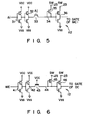
- Fig. 5 shows the construction of word line buffer 112 to which voltage SW is supplied.
- CMOS inverter 31 is supplied with signal Ai which is obtained by decoding the row address by use of decoder 110.
- An output of inverter 31 is supplied to CMOS inverter 32.
- an output of CMOS inverter 32 is supplied to node 34 via transistor 33 to which signal Aj obtained in the same manner as signal Ai is supplied.
- Depletion type transistor 35 having a gate connected to node 34 is connected between nodes 34 and 23. Further, a signal at node 34 is supplied to CMOS inverter 36 to which voltage SW is supplied.
- voltage SW or Vss is supplied from word line buffer 112 to control gate 75 of memory cell MCl via inverter 36 according to the input address.
- Fig. 6 shows the detail circuit construction of reference cell driving circuit 12.
- Write control signal WE which is set to logic level “1" when data is programmed into memory cell MCl and set to "0" at the other time is supplied to CMOS inverter 41.
- An output of inverter 41 is supplied to CMOS inverter 42 and an output of inverter 42 is supplied to node 44 via MOS transistor 43 whose gate is connected to receive power source voltage Vcc.
- Depletion type MOS transistor 45 is connected between nodes 44 and 23. Further, a signal at node 44 is supplied to CMOS inverter 46 to which voltage SW is supplied from node 23.
- signal WE is set at logic level "1" as shown in Fig. 7A when data is written into memory cell MCl.
- high voltage Vpp is output as voltage SW from voltage switching circuit 102 shown in Fig. 3.
- signals Ai and Aj are produced based on the input address, and one of voltage SW and ground voltage Vss is selected according to signals Ai and Aj in word line buffer 112 shown in Fig.5 and supplied to control gate 75 of memory cell MCl as shown in Fig. 7C.
- write control signal WE of logic level "1" is supplied to reference cell driving circuit 12 of Fig. 6 when data is programmed into memory cell MCl. Therefore, outputs of inverters 41 and 42 are respectively set to logic levels "0" and "1". As a result, voltage Vpp is supplied as voltage SW to node 44 via transistor 45, causing the N-channel MOS transistor of CMOS inverter 46 to be turned on and therefore voltage Vss of 0 V is applied to the control gate of reference cell DC as shown in Fig. 7D. Thus, high voltage Vpp is prevented from being applied to reference cell DC when data is written into memory cell MCl.
- signal WE When data is read out from memory cell MCl, signal WE is set at logic level "1" as shown in Fig. 7A. At this time, voltage Vcc is output from voltage switching circuit 102 as voltage SW as shown in Fig. 7B. Further, one of voltage SW and ground voltage Vss is selected based on signals Ai and Aj in word line buffer 112 of Fig. 3 and supplied to control gate of memory cell MCl. In this case, since voltage SW is at Vcc, voltage Vcc is applied to control gate 75 of a selected one of memory cells MCl. When data is read out from memory cell MCl, write control signal WE of logic level "0" is supplied to reference cell driving circuit 12 of Fig.
- inverters 41 and 42 are respectively set to logic levels "1" and "0". Therefore, current is caused to flow from node 23 via transistors 45 and 43 and the N-channel MOS transistor of CMOS inverter 42, thereby setting node 44 to ground voltage Vss. As a result, the P-channel MOS transistor of CMOS inverter 46 is turned on, causing voltage Vcc to be supplied as voltage SW to the control gate of reference cell DC as shown in Fig. 7D. In response to voltage Vcc, reference voltage generation circuit 122 supplies a preset reference potential to sense amplifier 116, which compares the reference potential with an output voltage of memory cell MCl and outputs the comparison result as readout data to the data line.
- voltage Vcc is applied to the control gate of the reference cell to generate a reference potential used in the sense amplifier only in the data readout mode.
- programming voltage Vpp is not applied to the control gate of the reference cell, causing no programming voltage stress and preventing electrons from being injected into the control gate.
- the reference cell driving circuit of Fig. 6 is controlled by write control signal WE, the reference potential is kept constant even if a different memory cell is selected.
- voltage Vcc applied to the control gate of the reference cell can be derived from an output voltage of voltage switching circuit 102 and is the same power source voltage as that for the memory cell.
- Fig. 8 shows the construction of reference cell driving circuit 12 according to another embodiment of this invention.
- write control signal WE when write control signal WE is at logic level "0" and potential at node 44 is set at logic level "0", current constantly flows from node 23 to ground voltage terminal Vss via transistors 45 and 43 and inverter 42, increasing the power consumption.
- CMOS gate circuit 49 constituted by P-channel MOS transistor 47 and N-channel MOS transistor 48 is used instead of CMOS inverter 46 of Fig. 6.
- the gate of transistor 47 is connected to node 44 and the gate of transistor 48 is connected to the output node of inverter 42.
- enhancement type P-channel MOS transistor 50 is connected between nodes 44 and 23 instead of depletion type MOS transistor 45.
- the gate of MOS transistor 50 is connected to the output node of gate circuit 49.
- P-channel MOS transistor 47 of gate circuit 49 is turned on and gate circuit 49 generates voltage SW when write-in control signal WE is at logic level "0" and the output of inverter 42 is set at logic level "0".
- P-channel transistor 50 is turned off, preventing current from flowing in a path from voltage terminal SW to ground voltage terminal Vss.
- write control signal WE is at logic level "1”
- the output of inverter 42 is set to logic level "1” and N-channel transistor 48 of gate circuit 49 is turned on, permitting gate circuit 49 to supply ground voltage Vss to the control gate of the reference cell.
Abstract
Description
- This invention relates to a nonvolatile semiconductor memory device in which a sense amplifier compares a sense potential generated from a memory cell, with a reference potential generated from a reference cell having the same structure as the memory cell to sense data, and more particularly to a semiconductor memory device having a reference cell transistor for generating the reference potential whose gate voltage can be controlled in the readout and write-in operations.
- Fig. 1 shows the schematic construction of a conventional semiconductor memory device, for example, a conventional electrically data programmable read only memory (EPROM). In Fig. 1, memory cell MCl (like memory cell MCn) is a stacked gate transistor. Fig. 2 is a cross sectional view showing the construction of memory cell MCl.
Source 72 anddrain 73 formed of n+-type diffusion regions are formed in the surface area of p-type substrate 71, floatinggate 74 is formed on that portion of the substrate which lies between the source and drain, andcontrol gate 75 is formed on the floating gate. The film thickness of that portion ofinsulation film 76 which lies betweensubstrate 71 and floatinggate 74 is set to tox1 and the film thickness of that portion ofinsulation film 76 which lies betweenfloating gate 74 andcontrol gate 75 is set to tox2. - Since the EPROM is a nonvolatile memory, data programmed into memory cell MCl can be permanently stored unless all the stored data is erased by application of ultraviolet rays. In this case, the "data programming" means that electrons are injected into
floating gate 74 of memory cell MCl and the data of the memory cell is set to "0". Memory cell MCl having data of "1" is in the erased state. In order to program data "0" into the memory cell, write-in voltage Vpp of 12.5 V, for example, is simultaneously applied to drain 73 and controlgate 75 of the memory cell, thereby causing hot electrons to be injected into the floating gate from the channel. As a result, the threshold voltage of the programmed memory cell transistor is raised and thus data is programmed into memory cell MCl of the EPROM. - In the readout mode, voltage Vcc of 5 V, for example, is applied to control
gate 75 to read out data stored in memory cell MCl. - As described above, in the EPROM, the level of a voltage applied to
control gate 75 when data is programmed into memory cell MCl is different from that applied when data is read out from the memory cell. Voltage Vcc (5 V) is applied in the data readout operation, and voltage Vpp (12.5 V) is applied in the data programming operation. Therefore, it is necessary to provide a switching circuit for internal power source which supplies voltages Vcc and Vpp in accordance with the internal state in addition to externally supplied power source voltages Vcc (5 V) and Vpp (12.5 V). - As shown in Fig. 1, the switching between voltages Vcc and Vpp is effected by use of
voltage switching circuit 102.Switching circuit 102 is supplied with data readout voltage Vcc viaterminal 142 and data programming voltage Vpp viaterminal 144. The voltage Vcc or Vpp as voltage SW is selectively supplied according to an programming control signal (write enable signal). Voltage Vpp is also supplied toprogramming control section 104.Programming control section 104 includestransistor 134 whose drain and source are respectively connected toterminal 144 and columnselection gate circuit 108 andprogramming control buffer 132 connected to receive voltage Vpp as a power source voltage for controlling the gate voltage oftransistor 134 according to programming data Din. -
Column decoder 106 decodes a column address included in the input address to output the decoded result to columnselection gate circuit 108.Circuit 108 includes N-channel MOS transistors and selectsbit line 120 based on the decoded result ofdecoder 106.Row decoder 110 decodes a row address included in the input address to output the decoded result toword line buffer 112.Buffer 112 is supplied with voltage SW fromcircuit 102 as the power source voltage and supplies a voltage to controlgate 75 of memory cell MCl. - The source and drain of memory cell MCl are respectively connected to ground voltage Vss and
bit line 120.Bit line 120 is connected to one input terminal ofsense amplifier 116 via transistors of columnselection gate circuit 108. Sense amplifier 116 senses "1" or "0" of data stored in memory cell MCl by comparing the potential ofsense line 123 varying according to data stored in one of memory cells MCl selected byrow decoder 110 andcolumn decoder 106 with a reference potential online 124 to be described later. - Reference
voltage generation circuit 122 supplies a reference voltage to senseamplifier 116.Circuit 122 includes reference cell DC constructed by the same stacked gate transistor as memory cell MCl and that is in the erased state normally turned-ontransistors 114 of the same number as the transistors series-connected in columnselection gate circuit 108. The gate of reference cell DC is supplied with power source voltage Vcc. The level of the reference voltage is determined by turning on reference cell DC. In order to obtain a stable reference potential, it is necessary to design the transistor characteristics of memory cell MCl and reference cell DC equal to each other. - With the above construction, when data is programmed into memory cell MCl, programming voltage Vpp is supplied as voltage SW from power
source switching circuit 102 to wordline buffer circuit 112. At the same time, programming voltage Vpp is supplied fromprogramming controlling buffer 12 to the gate ofprogramming controlling transistor 134. If the threshold voltage oftransistor 134 is Vth, a voltage of (Vpp-Vth) is supplied to the drain of memory cell MCl via columnselection gate circuit 108.Word line buffer 112 supplies programming voltage Vpp to the control gate of memory cell MCl. As a result, hot electrons are injected into floatinggate 74 to raise the threshold voltage of memory cell MCl. In this way, data is programmed into memory cell MCl. - When data is read out from memory cell MCl, voltage Vcc is supplied as voltage SW from power
source switching circuit 102 toword line buffer 112. At this time, voltage Vcc is supplied fromword line buffer 112 to the control gate of memory cell MCl. A voltage corresponding to data stored in memory cell MCl to be supplied tosense amplifier 116 via columnselection gate circuit 108. A reference voltage is also supplied from referencevoltage generating circuit 122 tosense amplifier 116. Then,sense amplifier 116 compares the voltage supplied from memory cell MCl with that supplied from reference cell DC and outputs the comparison result as readout data to the data line. - In the conventional EPROM, if power source voltage Vcc is varied by the influence of noise, the control gate voltage of the reference cell is also varied. However, since voltage SW is coupled with voltage Vcc via the transistor of
voltage switching circuit 102, variation in the control gate voltage of the memory cell will become different from that in the control gate voltage of the reference cell. As a result, the characteristics of the memory cell and reference cell may become different from each other in the data readout operation, thereby causing the sense amplifier to erroneously operate. - Conventionally, in order to make the characteristics of the memory cell and reference cell equal to each other, the control gates of the memory cell and reference cell may be commonly connected to receive the same power source voltage SW. However, in this case, programming voltage Vpp is supplied to the control gate of the reference cell when data is programmed into the memory cell. In the ordinary operation, no electron is injected into the floating gate of the reference cell, but in this case, electrons may be injected into the floating gate by the high voltage stress due to application of voltage Vpp to the control gate thereof although it is small in amount. Accordingly, when the memory device is used over a long period of time, the operation characteristic of the reference cell may be changed. Further, with this method, each time a new one of the memory cells is selected, a corresponding one of the reference cells is selected, and therefore the reference potential may be changed depending on the selection of reference cell.
- As described above, in the conventional semiconductor memory device, the gate of the reference cell is connected to directly receive the readout power source voltage and therefore there is a possibility that the sense amplifier may be erroneously operated by the influence of noise. Further, in the prior art, if the same voltage is supplied from the same power source to the control gates of the memory cell and reference cell in order to set the characteristics of the memory cell and reference cell equal to each other, the characteristic of the reference cell may be changed, or the reference potential may be changed when a new memory cell is selected, thus lowering the reliability thereof.
- This invention has been made in view of the above fact, and an object of this invention is to provide a highly reliable semiconductor memory device in which the operation characteristics of memory cells and reference cells can be set equal to each other without applying an unwanted voltage stress to the reference cell.
- In order to achieve the above object, a semiconductor memory device is characterized by comprising memory cells for storing data. The data being read out from the memory cell to generate a read voltage in a read mode and the data being written into the memory cell in a write mode; voltage switching circuit means for selectively generating one of first and second voltages according to a selected one of the read and write modes, the write modes being selectively set in response to a write-in control signal and the voltage switching circuit means generating the first voltage in the read mode and the second voltage in the write mode; a first driving circuit for driving the memory cell by a voltage output from the voltage switching circuit means according to a memory selection signal which is determined by an address; a sense amplifier for comparing a sense potential from the memory cell with a reference potential in the read mode to sense data stored in the memory cell; a reference cell for generating the reference potential in the read mode; and a second driving circuit for driving the reference cell by a voltage of the ground potential level in the write mode and by the first voltage in the read mode.
- In order to achieve the above object, a method for protecting a reference cell from an unwanted voltage stress in the write-in operation of a semiconductor memory device is characterized by comprising the steps of:
applying a first voltage for data write-in to the gate of a memory cell in the write mode and applying a second voltage to the gate of the memory cell so as to generate a read voltage corresponding to the data in the read mode;
applying a ground potential to the gate of a reference cell in the write mode and applying the second voltage to the gate of the reference cell in the read mode so as to generate a reference potential; and
comparing the read potential from the memory cell with the reference potential from the reference cell in the read mode to sense data stored in the memory cell. - As described above, according to this invention, a highly reliable semiconductor memory device in which the operation characteristics of the reference cell and memory cell can be made equal to each other without applying an unnecessary voltage stress to the reference cell can be obtained.
- This invention can be more fully understood from the following detailed description when taken in conjunction with the accompanying drawings, in which:
- Fig. 1 is a block diagram showing the schematic construction of the conventional EPROM;
- Fig. 2 is a cross sectional view showing the construction of a memory cell shown in Fig. 1;
- Fig. 3 is a block diagram showing the schematic construction of an EPROM to which this invention is applied;
- Fig. 4 is a block diagram showing the construction of a voltage switching circuit shown in Fig. 3;
- Fig. 5 is a circuit diagram showing the construction of a word line buffer shown in Fig. 3;
- Fig. 6 is a circuit diagram showing the construction of a reference cell driving circuit shown in Fig. 3;
- Figs. 7A to 7D are timing charts for illustrating the operation of the semiconductor memory device of this invention; and
- Fig. 8 is a circuit diagram showing another construction of the reference cell driving circuit.
- There will now be described a semiconductor memory device according to one embodiment of this invention with reference to the accompanying drawings. Portions which are the same as those shown in Fig. 1 are denoted by the same reference numerals and the explanation therefor is omitted.
- First, the construction of a semiconductor memory device according to the first embodiment of this invention is explained with reference to Fig. 3 by taking a nonvolatile semiconductor memory device (EPROM) as an example. In the EPROM provided as the semiconductor memory device according to this invention, an output of a word line buffer (first gate driving circuit) as shown in Fig. 1 is supplied to control gate 75 (Fig. 2) of memory cell MCl and an output of reference cell driving circuit (second driving circuit) 12 specifically shown in Fig. 6 is supplied to the control gate of reference cell DC.
- Fig. 4 shows the specific construction of
voltage switching circuit 102 shown in Fig. 3. As shown in Fig. 4, depletion type MOS transistor 21 whose gate is connected to receive inverted write control signal viavoltage converter 24 WE is connected betweenterminal 144 to which programming voltage Vpp is supplied andoutput voltage node 23 and depletion type MOS transistor 22 whose gate is connected to receive inverted signal of write control signal WE is connected betweenterminal 142 to which voltage Vcc is supplied andoutput voltage node 23. In this case, transistors 21 and 22 are of N-channel type. - In
circuit 102, write control signal WE is set to logic level "1" when data is programmed into memory cell MCl. As a result, transistor 21 is turned on to derive voltage Vpp as voltage SW atnode 23. Further, in the data readout mode, the write control signal WE is set to logic level "0" to turn on transistor 22, and as a result, voltage Vcc is generated as voltage SW. Voltage SW is supplied to control gate 75 (Fig. 2) of memory cell MCl viaword line buffer 112. - Fig. 5 shows the construction of
word line buffer 112 to which voltage SW is supplied. CMOS inverter 31 is supplied with signal Ai which is obtained by decoding the row address by use ofdecoder 110. An output of inverter 31 is supplied toCMOS inverter 32. Further, an output ofCMOS inverter 32 is supplied tonode 34 viatransistor 33 to which signal Aj obtained in the same manner as signal Ai is supplied.Depletion type transistor 35 having a gate connected tonode 34 is connected betweennodes node 34 is supplied toCMOS inverter 36 to which voltage SW is supplied. - In this way, voltage SW or Vss is supplied from
word line buffer 112 to controlgate 75 of memory cell MCl viainverter 36 according to the input address. - Fig. 6 shows the detail circuit construction of reference
cell driving circuit 12. Write control signal WE which is set to logic level "1" when data is programmed into memory cell MCl and set to "0" at the other time is supplied to CMOS inverter 41. An output of inverter 41 is supplied toCMOS inverter 42 and an output ofinverter 42 is supplied tonode 44 viaMOS transistor 43 whose gate is connected to receive power source voltage Vcc. Depletiontype MOS transistor 45 is connected betweennodes node 44 is supplied toCMOS inverter 46 to which voltage SW is supplied fromnode 23. - Now, the operation of the first embodiment of this invention is explained with reference to the timing chart shown in Figs. 7A to 7D.
- In the EPROM of Fig. 3, signal WE is set at logic level "1" as shown in Fig. 7A when data is written into memory cell MCl. At this time, as shown in Fig. 7B, high voltage Vpp is output as voltage SW from
voltage switching circuit 102 shown in Fig. 3. Further, inrow decoder 112 of Fig. 5, signals Ai and Aj are produced based on the input address, and one of voltage SW and ground voltage Vss is selected according to signals Ai and Aj inword line buffer 112 shown in Fig.5 and supplied to controlgate 75 of memory cell MCl as shown in Fig. 7C. That is, when signal Ai is at logic level "0", outputs ofinverters 31 and 32 are respectively set to logic levels "1" and "0". At this time, if signal Aj is at logic level "1",transistor 33 is turned on to set the potential ofnode 34 to logic level "0", and as a result, voltage SW which is set at high voltage Vpp is supplied frominverter 36 to controlgate 75 of memory cell MCl. - In this case, write control signal WE of logic level "1" is supplied to reference
cell driving circuit 12 of Fig. 6 when data is programmed into memory cell MCl. Therefore, outputs ofinverters 41 and 42 are respectively set to logic levels "0" and "1". As a result, voltage Vpp is supplied as voltage SW tonode 44 viatransistor 45, causing the N-channel MOS transistor ofCMOS inverter 46 to be turned on and therefore voltage Vss of 0 V is applied to the control gate of reference cell DC as shown in Fig. 7D. Thus, high voltage Vpp is prevented from being applied to reference cell DC when data is written into memory cell MCl. - When data is read out from memory cell MCl, signal WE is set at logic level "1" as shown in Fig. 7A. At this time, voltage Vcc is output from
voltage switching circuit 102 as voltage SW as shown in Fig. 7B. Further, one of voltage SW and ground voltage Vss is selected based on signals Ai and Aj inword line buffer 112 of Fig. 3 and supplied to control gate of memory cell MCl. In this case, since voltage SW is at Vcc, voltage Vcc is applied to controlgate 75 of a selected one of memory cells MCl. When data is read out from memory cell MCl, write control signal WE of logic level "0" is supplied to referencecell driving circuit 12 of Fig. 6 and outputs ofinverters 41 and 42 are respectively set to logic levels "1" and "0". Therefore, current is caused to flow fromnode 23 viatransistors CMOS inverter 42, thereby settingnode 44 to ground voltage Vss. As a result, the P-channel MOS transistor ofCMOS inverter 46 is turned on, causing voltage Vcc to be supplied as voltage SW to the control gate of reference cell DC as shown in Fig. 7D. In response to voltage Vcc, referencevoltage generation circuit 122 supplies a preset reference potential to senseamplifier 116, which compares the reference potential with an output voltage of memory cell MCl and outputs the comparison result as readout data to the data line. - As described above, according to the construction of this invention, voltage Vcc is applied to the control gate of the reference cell to generate a reference potential used in the sense amplifier only in the data readout mode. On the other hand, in the data write mode, programming voltage Vpp is not applied to the control gate of the reference cell, causing no programming voltage stress and preventing electrons from being injected into the control gate. Further, since the reference cell driving circuit of Fig. 6 is controlled by write control signal WE, the reference potential is kept constant even if a different memory cell is selected. In the data readout mode, voltage Vcc applied to the control gate of the reference cell can be derived from an output voltage of
voltage switching circuit 102 and is the same power source voltage as that for the memory cell. For this reason, even if voltage Vcc is varied by the influence of noise, voltages of the control gates of the reference cell and memory cell vary in the same manner. Therefore, the transistor characteristics of the reference cell and memory cell can be made equal to each other, preventing the sense amplifier from being erroneously operated by the influence of noise. - Fig. 8 shows the construction of reference
cell driving circuit 12 according to another embodiment of this invention. In the embodiment of Fig. 6, when write control signal WE is at logic level "0" and potential atnode 44 is set at logic level "0", current constantly flows fromnode 23 to ground voltage terminal Vss viatransistors inverter 42, increasing the power consumption. - In the embodiment of Fig. 8,
CMOS gate circuit 49 constituted by P-channel MOS transistor 47 and N-channel MOS transistor 48 is used instead ofCMOS inverter 46 of Fig. 6. The gate oftransistor 47 is connected tonode 44 and the gate oftransistor 48 is connected to the output node ofinverter 42. Further, enhancement type P-channel MOS transistor 50 is connected betweennodes type MOS transistor 45. The gate ofMOS transistor 50 is connected to the output node ofgate circuit 49. - With reference
cell driving circuit 12 of the above construction, P-channel MOS transistor 47 ofgate circuit 49 is turned on andgate circuit 49 generates voltage SW when write-in control signal WE is at logic level "0" and the output ofinverter 42 is set at logic level "0". As a result, P-channel transistor 50 is turned off, preventing current from flowing in a path from voltage terminal SW to ground voltage terminal Vss. On the other hand, when write control signal WE is at logic level "1", the output ofinverter 42 is set to logic level "1" and N-channel transistor 48 ofgate circuit 49 is turned on, permittinggate circuit 49 to supply ground voltage Vss to the control gate of the reference cell. - Reference signs in the claims are intended for better understanding and shall not limit the scope.
Claims (10)
a memory cell (MCl) connected to a ground potential, for storing data, the data being read out from said memory cell (MCl) in a read mode and the data being written into said memory cell (MCl) in a write mode;
potential switching means (102) for selectively generating one of first and second potentials in accordance with a mode set as one of the read and write modes, the write mode being set in response to a write control signal and said potential switching means (102) generating the first potential in the read mode and the second potential in the write mode;
first driving means (112) for driving said memory cell (MCl) in accordance with one of the first and second potentials from said potential switching means (102) in accordance with a memory cell selection signal which is determined by an input address;
sense amplifier means (116) for comparing a sense potential corresponding to the data from said memory cell (MCl) with a reference potential input thereto in the read mode to sense the data stored in said memory cell (MCl);
a reference cell (DC) connected to the ground potential, for generating and outputting the reference potential to said sense amplifier means (116) in the read mode; and
second driving means (12) connected to the ground potential, for driving said reference cell (DC) in accordance with the reference potential in the write mode and the output of said potential switching means (102) in the read mode as a drive potential.
a first transistor (43) connected to a first node, for setting said first node to the ground potential in the read mode;
a second transistor (45) connected between said first node and said potential switching means (102), for setting said first node to a potential determined in accordance with the second potential from said potential switching means (102) in the write mode; and
a CMOS gate circuit (46) for receiving one of the first and second potentials from said potential switching means (102), for driving said reference cell (DC) in accordance with the potential of said first node.
a first transistor (43) connected between first and second nodes, for setting said first node to the ground potential in the read mode, the potential of said second node being set to the ground potential in the read mode and to the first potential in the write mode;
a second transistor (45) connected between said first node and said potential switching means (102), for setting said first node to a potential determined in accordance with the second potential from said potential switching means (102) in the write mode;
a P-channel MOS transistor (47) supplied with one of the first and second potentials from said potential switching means (102), for driving said reference cell (DC) in accordance with the potential of said first node, and
an N-channel MOS transistor (48) connected to said P-channel MOS transistor (47), for driving said reference cell (DC) in accordance with the potential of said second node.
a first transistor (43) for potential separation connected between a terminal to which the write control signal is supplied and a first node;
a second transistor (45) connected between said first node and said potential switching means (102) for charging said first node; and
a CMOS gate circuit (46) supplied with one of the first and second potentials from said potential switching means (102) for operating in accordance with a potential of said first node.
a first transistor (43) for potential separation connected between a terminal to which the write control signal is supplied and a first node;
a CMOS gate circuit (47, 48) supplied with one of the first and second potentials from said potentials switching means (102) and connected to receive the write control signal and a signal of said first node;
and
a second transistor (50) for charging connected between said first node and said potential switching means (102) and having a gate connected to an output of said CMOS gate circuit.
applying a first potential to the gate of a memory cell in a read mode to generate a sense potential corresponding to data and applying a second potential for data write to the gate of said memory cell in the write mode;
applying a ground potential to a gate of a reference cell in the write mode and applying the first potential to the gate of said reference cell in the read mode so as to generate a reference potential; and
comparing the sense potential from said memory cell with the reference potential from said reference cell in the read mode to sense the data stored in said memory cell.
setting a first node to the ground potential in the read mode;
setting said first node to the second potential in the write mode; and
applying the ground potential to the gate of said reference cell in the write mode or applying the first potential to the gate of said reference cell in the read mode in accordance with a potential of said first node.
setting a first node to the ground potential in the read mode;
setting a potential of a second node to the ground potential in the read mode and to the first potential in the write mode;
setting a potential of said first node to the second potential in the write mode;
applying the first potential to the gate of said reference cell in accordance with the potential of said first node in the read mode; and
applying the ground potential to the gate of said reference cell according to the potential of said second node.
Applications Claiming Priority (2)
| Application Number | Priority Date | Filing Date | Title |
|---|---|---|---|
| JP743489A JPH0814994B2 (en) | 1989-01-13 | 1989-01-13 | Semiconductor memory device |
| JP7434/89 | 1989-01-13 |
Publications (3)
| Publication Number | Publication Date |
|---|---|
| EP0377840A2 true EP0377840A2 (en) | 1990-07-18 |
| EP0377840A3 EP0377840A3 (en) | 1991-05-29 |
| EP0377840B1 EP0377840B1 (en) | 1995-02-08 |
Family
ID=11665761
Family Applications (1)
| Application Number | Title | Priority Date | Filing Date |
|---|---|---|---|
| EP89122914A Expired - Lifetime EP0377840B1 (en) | 1989-01-13 | 1989-12-12 | Nonvolatile semiconductor memory device having reference potential generating circuit |
Country Status (5)
| Country | Link |
|---|---|
| US (1) | US4974206A (en) |
| EP (1) | EP0377840B1 (en) |
| JP (1) | JPH0814994B2 (en) |
| KR (1) | KR920009058B1 (en) |
| DE (1) | DE68921062T2 (en) |
Cited By (3)
| Publication number | Priority date | Publication date | Assignee | Title |
|---|---|---|---|---|
| EP0484298A2 (en) * | 1990-10-31 | 1992-05-06 | SGS-THOMSON MICROELECTRONICS S.p.A. | Flash-EPROM with enhanced immunity from soft-programming of reference cells |
| EP0505051A1 (en) * | 1991-03-19 | 1992-09-23 | National Semiconductor Corporation | Data storage system with intrinsic burst detection |
| GB2232798B (en) * | 1989-06-12 | 1994-02-23 | Intel Corp | Electrically programmable read-only memory |
Families Citing this family (8)
| Publication number | Priority date | Publication date | Assignee | Title |
|---|---|---|---|---|
| US5327392A (en) * | 1989-01-13 | 1994-07-05 | Kabushiki Kaisha Toshiba | Semiconductor integrated circuit capable of preventing occurrence of erroneous operation due to noise |
| KR950004870B1 (en) * | 1992-11-24 | 1995-05-15 | 삼성전자 주식회사 | Isolation gate circuit with improved reliability in burn-in mode |
| KR100316521B1 (en) * | 1999-01-18 | 2001-12-12 | 김영환 | Over drive circuit for semiconductor memory |
| US6538922B1 (en) * | 2000-09-27 | 2003-03-25 | Sandisk Corporation | Writable tracking cells |
| US7237074B2 (en) * | 2003-06-13 | 2007-06-26 | Sandisk Corporation | Tracking cells for a memory system |
| US7301807B2 (en) | 2003-10-23 | 2007-11-27 | Sandisk Corporation | Writable tracking cells |
| JP4199765B2 (en) * | 2005-12-02 | 2008-12-17 | マイクロン テクノロジー,インコーポレイテッド | High voltage switching circuit |
| US10134477B2 (en) * | 2016-10-28 | 2018-11-20 | Samsung Electronics Co., Ltd. | Nonvolatile memory device detecting power noise and operating method thereof |
Citations (1)
| Publication number | Priority date | Publication date | Assignee | Title |
|---|---|---|---|---|
| EP0244628A1 (en) * | 1986-03-31 | 1987-11-11 | Kabushiki Kaisha Toshiba | Sense amplifier for a semiconductor memory device |
Family Cites Families (4)
| Publication number | Priority date | Publication date | Assignee | Title |
|---|---|---|---|---|
| JPS61270921A (en) * | 1985-05-25 | 1986-12-01 | Toshiba Corp | Decoder circuit |
| JPS6231094A (en) * | 1985-08-01 | 1987-02-10 | Toshiba Corp | Non-volatile semiconductor memory device |
| JPS6276098A (en) * | 1985-09-30 | 1987-04-08 | Toshiba Corp | Sense amplifier circuit |
| DE3768277D1 (en) * | 1987-12-15 | 1991-04-04 | Ibm | REFERENCE VOLTAGE GENERATOR FOR CMOS MEMORY. |
-
1989
- 1989-01-13 JP JP743489A patent/JPH0814994B2/en not_active Expired - Lifetime
- 1989-12-04 US US07/444,986 patent/US4974206A/en not_active Expired - Lifetime
- 1989-12-12 EP EP89122914A patent/EP0377840B1/en not_active Expired - Lifetime
- 1989-12-12 DE DE68921062T patent/DE68921062T2/en not_active Expired - Fee Related
-
1990
- 1990-01-13 KR KR1019900000398A patent/KR920009058B1/en not_active IP Right Cessation
Patent Citations (1)
| Publication number | Priority date | Publication date | Assignee | Title |
|---|---|---|---|---|
| EP0244628A1 (en) * | 1986-03-31 | 1987-11-11 | Kabushiki Kaisha Toshiba | Sense amplifier for a semiconductor memory device |
Cited By (6)
| Publication number | Priority date | Publication date | Assignee | Title |
|---|---|---|---|---|
| GB2232798B (en) * | 1989-06-12 | 1994-02-23 | Intel Corp | Electrically programmable read-only memory |
| US5390146A (en) * | 1989-06-12 | 1995-02-14 | Intel Corporation | Reference switching circuit for flash EPROM |
| EP0484298A2 (en) * | 1990-10-31 | 1992-05-06 | SGS-THOMSON MICROELECTRONICS S.p.A. | Flash-EPROM with enhanced immunity from soft-programming of reference cells |
| EP0484298A3 (en) * | 1990-10-31 | 1993-02-24 | Sgs-Thomson Microelectronics S.P.A. | Flash-eprom with enhanced immunity from soft-programming of reference cells |
| US5311466A (en) * | 1990-10-31 | 1994-05-10 | Sgs-Thomson Microelectronics S.R.L. | FLASH-EPROM with enhanced immunity from soft-programming of reference cells |
| EP0505051A1 (en) * | 1991-03-19 | 1992-09-23 | National Semiconductor Corporation | Data storage system with intrinsic burst detection |
Also Published As
| Publication number | Publication date |
|---|---|
| KR900012282A (en) | 1990-08-03 |
| JPH0814994B2 (en) | 1996-02-14 |
| JPH02187996A (en) | 1990-07-24 |
| US4974206A (en) | 1990-11-27 |
| DE68921062T2 (en) | 1995-07-20 |
| EP0377840B1 (en) | 1995-02-08 |
| DE68921062D1 (en) | 1995-03-23 |
| KR920009058B1 (en) | 1992-10-13 |
| EP0377840A3 (en) | 1991-05-29 |
Similar Documents
| Publication | Publication Date | Title |
|---|---|---|
| US5097152A (en) | Buffer circuit used in a semiconductor device operating by different supply potentials and method of operating the same | |
| KR100338772B1 (en) | Word line driver having divided bias line in non-volatile memory device and method thereof | |
| US5463583A (en) | Non-volatile semiconductor memory device | |
| EP0052566A2 (en) | Electrically erasable programmable read-only memory | |
| US4733371A (en) | Semiconductor memory device with high voltage switch | |
| US20020030204A1 (en) | Voltage level shifter circuit and nonvolatile semiconductor storage device using the circuit | |
| KR960005370B1 (en) | Method for erasing and verifying nonvolatile semiconductor memory device | |
| EP0377839A2 (en) | Semiconductor memory device capable of preventing data of non-selected memory cell from being degraded | |
| EP0377840A2 (en) | Nonvolatile semiconductor memory device having reference potential generating circuit | |
| JPH0793022B2 (en) | Semiconductor memory integrated circuit | |
| US5297095A (en) | Semiconductor non-volatile memory device improved in verifying operation for erased and write-in states | |
| EP0345791A2 (en) | Nonvolatile semiconductor memory | |
| KR940005694B1 (en) | Program optimization circuit and method of eeprom | |
| EP0368310A2 (en) | Nonvolatile memory device capable of outputting correct read data at proper time | |
| JP2510521B2 (en) | EEPROM device | |
| US5896319A (en) | Current control circuit and non-volatile semiconductor memory device having the same | |
| JP3362661B2 (en) | Nonvolatile semiconductor memory device | |
| KR930001653B1 (en) | Nonvolatile semiconductor memory device | |
| JPH09153294A (en) | Semiconductor memory device | |
| EP0377841A2 (en) | Semiconductor integrated circuit capable of preventing occurrence of erroneous operation due to noise | |
| JPH06349285A (en) | Nonvolatile semiconductor memory | |
| JPH06338197A (en) | Address decoder circuit | |
| KR100308120B1 (en) | Semiconductor memory device ahving static burn-in test circuit | |
| JP2714478B2 (en) | Nonvolatile semiconductor memory device | |
| JP2509023B2 (en) | Decoder circuit |
Legal Events
| Date | Code | Title | Description |
|---|---|---|---|
| PUAI | Public reference made under article 153(3) epc to a published international application that has entered the european phase |
Free format text: ORIGINAL CODE: 0009012 |
|
| 17P | Request for examination filed |
Effective date: 19891212 |
|
| AK | Designated contracting states |
Kind code of ref document: A2 Designated state(s): DE FR GB |
|
| PUAL | Search report despatched |
Free format text: ORIGINAL CODE: 0009013 |
|
| AK | Designated contracting states |
Kind code of ref document: A3 Designated state(s): DE FR GB |
|
| 17Q | First examination report despatched |
Effective date: 19931022 |
|
| GRAA | (expected) grant |
Free format text: ORIGINAL CODE: 0009210 |
|
| AK | Designated contracting states |
Kind code of ref document: B1 Designated state(s): DE FR GB |
|
| REF | Corresponds to: |
Ref document number: 68921062 Country of ref document: DE Date of ref document: 19950323 |
|
| ET | Fr: translation filed | ||
| PLBE | No opposition filed within time limit |
Free format text: ORIGINAL CODE: 0009261 |
|
| STAA | Information on the status of an ep patent application or granted ep patent |
Free format text: STATUS: NO OPPOSITION FILED WITHIN TIME LIMIT |
|
| 26N | No opposition filed | ||
| REG | Reference to a national code |
Ref country code: GB Ref legal event code: IF02 |
|
| PGFP | Annual fee paid to national office [announced via postgrant information from national office to epo] |
Ref country code: GB Payment date: 20061206 Year of fee payment: 18 |
|
| PGFP | Annual fee paid to national office [announced via postgrant information from national office to epo] |
Ref country code: DE Payment date: 20061207 Year of fee payment: 18 |
|
| PGFP | Annual fee paid to national office [announced via postgrant information from national office to epo] |
Ref country code: FR Payment date: 20061208 Year of fee payment: 18 |
|
| GBPC | Gb: european patent ceased through non-payment of renewal fee |
Effective date: 20071212 |
|
| PG25 | Lapsed in a contracting state [announced via postgrant information from national office to epo] |
Ref country code: DE Free format text: LAPSE BECAUSE OF NON-PAYMENT OF DUE FEES Effective date: 20080701 |
|
| REG | Reference to a national code |
Ref country code: FR Ref legal event code: ST Effective date: 20081020 |
|
| PG25 | Lapsed in a contracting state [announced via postgrant information from national office to epo] |
Ref country code: GB Free format text: LAPSE BECAUSE OF NON-PAYMENT OF DUE FEES Effective date: 20071212 |
|
| PG25 | Lapsed in a contracting state [announced via postgrant information from national office to epo] |
Ref country code: FR Free format text: LAPSE BECAUSE OF NON-PAYMENT OF DUE FEES Effective date: 20071231 |