EP0380855A2 - Memory configuration for use with means for interfacing a system control unit for a multi-processor system with the system main memory - Google Patents
Memory configuration for use with means for interfacing a system control unit for a multi-processor system with the system main memory Download PDFInfo
- Publication number
- EP0380855A2 EP0380855A2 EP89309275A EP89309275A EP0380855A2 EP 0380855 A2 EP0380855 A2 EP 0380855A2 EP 89309275 A EP89309275 A EP 89309275A EP 89309275 A EP89309275 A EP 89309275A EP 0380855 A2 EP0380855 A2 EP 0380855A2
- Authority
- EP
- European Patent Office
- Prior art keywords
- memory
- data
- scu
- segments
- command
- Prior art date
- Legal status (The legal status is an assumption and is not a legal conclusion. Google has not performed a legal analysis and makes no representation as to the accuracy of the status listed.)
- Granted
Links
Images


Classifications
-
- G—PHYSICS
- G06—COMPUTING; CALCULATING OR COUNTING
- G06F—ELECTRIC DIGITAL DATA PROCESSING
- G06F13/00—Interconnection of, or transfer of information or other signals between, memories, input/output devices or central processing units
- G06F13/14—Handling requests for interconnection or transfer
- G06F13/16—Handling requests for interconnection or transfer for access to memory bus
- G06F13/1605—Handling requests for interconnection or transfer for access to memory bus based on arbitration
- G06F13/1652—Handling requests for interconnection or transfer for access to memory bus based on arbitration in a multiprocessor architecture
- G06F13/1663—Access to shared memory
-
- G—PHYSICS
- G06—COMPUTING; CALCULATING OR COUNTING
- G06F—ELECTRIC DIGITAL DATA PROCESSING
- G06F12/00—Accessing, addressing or allocating within memory systems or architectures
- G06F12/02—Addressing or allocation; Relocation
- G06F12/06—Addressing a physical block of locations, e.g. base addressing, module addressing, memory dedication
- G06F12/0607—Interleaved addressing
-
- G—PHYSICS
- G06—COMPUTING; CALCULATING OR COUNTING
- G06F—ELECTRIC DIGITAL DATA PROCESSING
- G06F15/00—Digital computers in general; Data processing equipment in general
- G06F15/76—Architectures of general purpose stored program computers
- G06F15/80—Architectures of general purpose stored program computers comprising an array of processing units with common control, e.g. single instruction multiple data processors
- G06F15/8007—Architectures of general purpose stored program computers comprising an array of processing units with common control, e.g. single instruction multiple data processors single instruction multiple data [SIMD] multiprocessors
- G06F15/8015—One dimensional arrays, e.g. rings, linear arrays, buses
Definitions
- This invention relates generally to multiprocessor computer systems. More particularly, this invention relates to a memory configuration suitable for use with an interface provided between the system control unit used for operating a plurality of processors in a parallel fashion and the main system memory in a multi-processing system for efficient interaction between each of the plurality of processors and the various modules comprising the system memory.
- the invention also relates to a system control unit (SCU).
- SCU system control unit
- VAX The "VAX" brand family of computers from Digital Equipment Corporation, Maynard, Massachusetts 01754, is aimed at computing needs falling mid-range of the performance spectrum; this family of computers has been extremely successfully by virtue of ease-of-programming, compatibility, good cost/performance ratio, and higher reliability.
- VAX Very Recently-programming
- High performance computers are generally based upon the concept of multi-processing at the system level wherein a plurality of processors are used to work on a defined task through appropriate problem decomposition.
- Such multi-processing is also complemented by the process of pipelining, in which a given computer instruction is divided into a series of smaller and less complex operations which are executed in a pipeline fashion by several dedicated functional units that are optimized for specific purposes.
- multiple I/O buses are used to provide parallel paths to mass storage and other devices in order to achieve high speed and extensive connectivity and redundancy.
- a system control unit may be used to coordinate the parallel operation of the plurality of central processor units (CPU's) comprising the multi-processing system in conjunction with the main system memory, I/O devices and other components of the computing system.
- CPU's central processor units
- each of the system components must be ported into the SCU which in turn has to link all ports together in a manner analogous to functions traditionally provided by system buses.
- the SCU functions, among other things, to keep all system components active while avoiding inter-unit conflicts by the use of extensive communication and validity checking.
- each of the system units, particularly the CPU's, to independently access memory is critical to realizing efficient parallel and pipelined operation, and one of the main functions of the SCU is to manage memory access in a manner which most efficiently allows the system units to run in parallel.
- a critical aspect of this operation is providing an efficient SCU/main memory interface which regulates parallel access for each of the system CPU's to the various modules comprising the main memory of the system. It is also important that the system memory be configured and controlled in a manner which is compatible with and particularly adapted to the provision of such an efficient interface.
- a memory configuration adapted for use with interface means between a System Control Unit (SCU) and a main memory in a multi-processing system comprises at least one memory unit containing independently accessible DRAM based memory segments, each memory unit comprising means for providing a first dedicated data path for the transfer of read data (the "read path") from address memory segments to the interface means for transfer to the SCU, means for providing a second dedicated data path (the “write path”) for transfer of write data received from the SCU through the interface means to addressed memory segments, and means for providing a third dedicated path for transfer of memory addresses (the "address path”) from the SCU for identification of addressed memory segments.
- SCU System Control Unit
- each MMU of the main memory is split between two memory ports on the SCU and the data storage section of each MMU comprises a pair of segments each comprising a pair of DRAM based memory banks.
- the memory addresses for the memory banks are interleaved on boundaries of blocks having a predetermined size corresponding to the size of cache blocks used in the system CPUs.
- Each memory segment is operated independently while a common data path is shared by the segments.
- the two banks comprising each MMU segment are controlled in such a way that only one bank may be active for a given memory command by providing different address lines to the segments while retaining common data lines.
- a single MMU is made up of a plurality of memory modules (MMs) each comprising a main array card (MAC) module which provides buffering of write and read data, maintains integrity of DRAM data during power failure, and provides connections and logic support for additional storage modules.
- DRAM data path (DDP) modules are provided on each memory module for handling level translation between logic levels, provision of the read data path and related buffering, provision of the right data path and related buffering, and provision of a DRAM by-pass path for special memory operations.
- Each memory module also includes a DRAM control and address (DCA) module for level translation, buffering of DRAM-related control signals, and generation of appropriate system control commands.
- DCA DRAM control and address
- the memory configuration according to this invention is particularly adapted for use with dedicated interface means provided between the SCU and the system main memory of the type disclosed in the above mentioned co-pending application Serial No. 306,326, filed February 3, 1989, by Gagliardo et al. titled “Method And Means For Interfacing A System Control Unit For A Multi-Processor System With The System Main Memory," the disclosure in which is incorporated in full herein by reference.
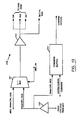
- FIG. 1 there is shown a simplified block diagram of a multiprocessing system 10 which uses a plurality of central processing units (CPUs) 12 and is configured to permit simultaneous, i.e., parallel operation, of the system CPUs by allowing them to share a common main memory 16 for the system.
- the main memory 16 itself typically comprises a plurality of memory modules or units 16A and 16B.
- a system control unit (SCU) 14 links the CPUs 12 to the main memory 16 and to the input output (I/O) controller 18 which allows the processing system in general and the CPUs in particular to communicate with the external world through appropriate I/O interfaces 20 and associated I/O units 20A for the system.
- I/O input output
- the SCU 14 also links the various system modules to a service processor/console unit (SPU) 22 which performs traditional console functions including status determination and the control of the overall operation of the processing system.
- SPU service processor/console unit
- the SCU 14 provides the SPU 22 with means for communicating with the plurality of CPUs 12 and provides access to all storage elements in the CPUs.
- Efficient communication between all system units ported into the SCU 14 and the main memory 16, and more particularly between each of the CPUs 12 and the main memory 16, is critical for insuring efficient parallel operation of the processing system.
- this critical operation is provided by means of a dedicated interface means 30 linking the SCU 14 and the main memory 16.
- the interface 30 provides the SCU 14 with means for interfacing and controlling the various modules comprising the main memory 16 in response to memory interaction commands or signals received from each of the CPUs 12 or I/O units 20A that are ported into the SCU.
- each CPU 12 typically includes a memory module 24 which provides the CPU interface to memory, I/O and other CPU units.
- the memory module serves as means for accepting memory references, usually virtual, translating the references to physical addresses, and initiating accesses to memory data, either in main memory through the SCU 14 and the interface means 30 or within a local cache.
- Each CPU 12 also includes an instruction module 26 for fetching instructions, decoding operation codes (op-codes) and specifiers, fetching operands, and updating the system program counter.
- each CPU has an execution module 28 which serves as the execution stage for decoded instructions and fetched operands provided by the other CPU modules.
- the interface means 30 is provided in the form of a memory sub-system 32 essentially comprising an array control unit (ACU) 34 which accepts command signals and data transfer requests from the SCU and a main memory unit (MMU) 36 functioning as the storage section of main memory 16 to which the SCU 14 is interfaced.
- ACU array control unit
- MMU main memory unit
- the ACU 34 includes all the control logic for providing the interfacing action and is preferably located physically on the SCU module itself.
- the interfacing of the SCU 14 to the main memory 16 is provided by means of the ACU 34 through a bi-sectional interface comprising (i) the ACU 34 and the links between the SCU 14 and the ACU 34 (collectively designated as 30A) and (ii) the link between the ACU 34 and a MMU 36 of main memory 16 (collectively designated as 30B).
- the following description will focus on the ACU, its links with the SCU, and its operation in providing the SCU with means through which transfer of memory commands, and associated data and address data, to and from the storage modules in the main memory may be accomplished.
- a memory configuration for the MMU 36 which is particularly adapted for use with the efficient interfacing action of the ACU 34 will also be provided.
- the SCU 14 is preferably interfaced to a main memory which has a non-bused, high bandwidth, and block oriented configuration. All CPU accesses to or from memory are made through the ACU 34 in block increments comprising a selected number of bytes (typically 64 bytes). Data storage in the main memory is provided through the use of extended hex-size modules, each preferably providing 64 megabits (M-bit) of storage using a one M-bit DRAM. Four such memory modules are grouped together to form a single MMU 36 and the main memory 16 includes at least one such MMU.
- M-bit megabits
- the ACU 34 provides the interface and control for the memory modules included within the MMU 36 and includes means for accepting a command/status/index signal over control line 38 from the SCU 14 indicative of the particular memory operation that is required, such as, read-from-memory, write-to-memory, etc. This signal also indicates the status of buffers within the logic portion of the SCU designated for receiving commands back from the ACU.
- the SCU 14 accepts memory access commands from requesting system units (such as CPUs or I/O units), decodes the command, initiates the translation of virtual addresses to physical addresses so as to correspond to byte address in the MMU segments, identifies and prioritizes non-conflicting memory accesses which may be executed, and generates command signals for initiating the execution of memory operations by transfer of data to and from memory.
- requesting system units such as CPUs or I/O units
- the operation of the ACU in providing the interfacing action is independent of the manner in which the pre-execution prioritizing and decoding is accomplished by the SCU. It is merely required that row/column addresses associated with memory access operations being requested by a system unit be stored in separate address registers in the control logic section of the SCU. The SCU then only needs to relay to the ACU information indicative of the particular memory port or segment that is the object of a particular memory operation; the associated row/column address can be relayed directly from the SCU to the MMU on the basis of a signal or index field from the ACU identifying the particular SCU address register to be used as the source of the row/column address.
- a direct address path 42 is provided between the SCU 14 and the corresponding MMU 36 so that the row/column address designating a particular segment of memory being addressed by a memory command can be transferred directly from the SCU 14 to the corresponding MMU 36 under control of the ACU 34.
- the command signal relayed from the SCU on line 38 includes an index which is used by the ACU as a basis for initiating direct transfer, from the SCU, of designated ones of the stored addresses referencing desired rows or columns within addressed memory segments in the MMU 36.
- the ACU accepts the index accompanying a memory command over the command/status signal line 38 and relays the index back if and when the particular memory segment being referenced by the command is available to be accessed.
- the memory access requests prioritized by the SCU for being executed are stored within address registers provided in the SCU.
- the execution of the particular memory command selected by the SCU for being executed at a given time is initiated by transmission of a load command to the ACU along with an index identifying the location of the corresponding memory address in the SCU address registers.
- the ACU subsequently receives the index and the associated memory command information which includes a designation of the memory segment/bank to be accessed. If the ACU determines, through its links to the MMU, that the desired memory segment is indeed available the associated index is relayed back to the SCU so that the corresponding row/column address identified by the index may be transferred directly to the MMU over the row/column address path between the SCU and the MMU.
- the ACU continues monitoring the segment and relays the index back to the SCU only when the address segment becomes available.
- the ACU through suitable buffering, continues the processing, on a sequential basis, of other memory access commands which are logged with the SCU and require access to a memory segment which is available at the time. More specifically, as will be described below, the ACU uses a command buffer for each memory segment for accepting an incoming memory command corresponding to a segment while a current memory command related to the same segment is being executed.
- the use of the index also permits the ACU to control multiplexed signals relayed over the address lines from the SCU 14 to the MMU 36.
- the ACU relays the index back to the SCU over the command/status line when it is ready to execute the associated memory command.
- the index relayed back to the SCU 14 identifies the stored row/column address which corresponds to a particular available segment of memory within the MMU. Receipt of the relayed index from the ACU initiates the transfer of the corresponding row/column address stored in the SCU over line 42 directly to the MMU.
- the index represents a predefined bit field in the command information transferred from the SCU to the ACU, which identifies one of the plurality of address registers provided within the SCU for storing row/column addresses associated with memory commands prioritized for execution by the SCU.
- the index preferably has a 4-bit field so that it is capable of identifying one of up to 16 address registers.
- Row/column addresses are transmitted in a multiplexed manner over the direct address path from the SCU to the MMU.
- the ACU also relays back to the SCU a signal, preferably in the form of a single bit added to the index field, which serves as a row/column select signal indicative of whether a row or column is being addressed in a memory segment by the address directly transmitted from the selected SCU address register to memory.
- the ACU also relays back with the index a signal, preferably a single bit signal, indicative of the particular one of the row and column addresses stored in the SCU address registers.
- the multiplexing of row addresses with column addresses is performed on the basis of the row/column select signal generated by the ACU by means of a standard multiplexing arrangement (not shown) provided within the SCU.
- the row/column select signal can be used to index up to 12 addresses, thereby making it possible to support addressability of up to 16M-bits of memory.
- the index associated with a memory command preferably includes at least one designated code bit for identifying the system CPU or an I/O unit originating the memory operation being executed; this facilitates prioritizing of memory commands and helps routing of accessed data appropriately through the ACU and SCU to the system unit originating the command.
- such an arrangement allows memory commands to be executed according to different predefined procedures depending on whether requesting unit is a system CPU or an I/O unit. For instance, it may be desirable to restrict write operation by a CPU to a selected number of quad-words, typically eight quad-words at one time while allowing I/O units to write anywhere from one byte up to number of bytes permitted for CPU writes.
- the ACU 34 is also linked to the SCU 14 through a communication line 40 through which a command/status signal is relayed to the SCU for providing an indication of availability and status of data requested from memory by the SCU.
- Data communication lines 44 and 46 serve as means for transfer of data between the SCU and the ACU. It should be noted that the ACU 34 does not serve as a means for storing data for subsequent transfer to or from the SCU; instead, the ACU merely functions as a means for relaying data on-the-fly from addressed portions of memory modules within the MMU to the SCU or vice versa.
- the modular composition of the ACU and its operation in providing the above function will be described in detail below.
- the ACU is linked to the MMU 36 by means of communication line 48 for transfer of control/command signals from the ACU indicative of the particular memory operation desired by the SCU.
- Communication line 50 serves as a means for transfer of the status of requested data from the MMU to the ACU.
- Data communication lines 52, 54 are provided as means a for transfer of data between the ACU and the MMU.
- the ACU 34 is linked to the SPU 22 through a control line 56.
- This link serves as a means for adapting the ACU, and hence the interfacing action provided by it, to the various timing modes between which the main memory may be switched.
- the SPU 22 is linked to the main memory via control line 58 and status line 60 in order to initialize the memory and switch the memory between three different timing modes: (1) a normal mode for supporting regular system operation; (2) a step mode to support single-step operation on the basis of system clocks; and (3) a stand-by mode for retaining system integrity during power failure and scan operation.
- the switching action is performed by the SPU 22 in responses to the transfer of appropriate signals from the SCU 14 via control lines 62 and 64.
- the communication link provided by line 56 between the ACU and the SPU permits the operation of the SCU-ACU interface for the SCU to be consistent with the memory mode in operation at a given time.
- clock means 66 for operating the interface to access memory is conveniently provided through clock means 66 provided on the SCU.
- the clock means 66 is preferably a programmable clock capable of generating a plurality of time-staggered clock signals having preselected clock periods.
- Such clocks are conventional and available in the form of I.C.s typically generating up to eight clock signals with different time periods. Different ones of the clock signals may be selected to control memory access on the basis of the clock period best suited for optimal data transfer timing as well as the mode under which the system is operating at a given time.
- FIG. 2 shows the interface between the SCU and the main memory as comprising a single memory sub-system 32 which includes a single MMU 36 and a corresponding ACU 34, it will be understood that additional MMU-ACU pairs or memory sub-systems may be used to permit the system CPUs to share increased memory.
- each MMU 36 of the main memory 16 is split between two memory ports on the SCU with each port having two segments and all segments being interleaved on block boundaries.
- the SCU can then be used to cycle all four segments in parallel through use of a single memory sub-system thereby permitting up to four memory references to be operated upon in a parallel fashion; in such a case, the ACU allows the SCU 14 to accept a memory request from any of the CPUs and to pass it on to the designated segment in memory.
- the interleaving of segments is based on matching the memory access block size to the size of the cache blocks used in the system CPUs.
- each MMU forming the main memory A preferred segment-based organization for each MMU forming the main memory is illustrated at FIG. 2A.
- the data storage section of each MMU 36 comprises a pair of segments 124, 126 each of which comprises a pair of memory banks.
- the four memory banks are respectively designated as 128, 130, 132, and 134.
- the memory banks are DRAM-based and may each store, for example, up to 64 Megabytes of data.
- FIG. 2A wherein interleaving is shown for a preferred data block size of 64 bytes.
- a first block (BLOCK 0) has byte addresses 0-63 associated with it and is stored in the first bank 128 of the first memory segment 124; the next consecutive block comprising byte addresses 64-127, i.e., the second block (BLOCK 1), is stored in the first memory bank 132 of the second memory segment 126; the third block (BLOCK 2) having byte addresses 128-191 associated with it is stored in the second memory bank 130 of the first memory segment 124; the fourth memory block (BLOCK 3) has byte addresses 192-225 associated with it and is stored in the second memory block 134 of the second memory segment 126; the fifth block (BLOCK 4) has byte addresses of 256-319 associated with it and is stored in the first memory bank 128 of the first memory segment 124; and so on.
- the main memory 36 comprised of the plurality of memory modules is provided with an access control circuit 136 which permits independent and simultaneous access to a plurality of the memory banks for obtaining blocks of data spread over different ranges of byte addresses.
- the choice of the data block size on which interleaving of memory segments is based is matched to the size of the cache blocks used in the various CPU's comprising the multi-processor system to maintain a correspondence between data blocks requested by a CPU and the corresponding interleaved data blocks available from the segments of each MMU.
- the ACU logic is implemented in macro-cell arrays and essentially provides the data path and control for the memory system.
- the ACU includes a main memory control (MMC) module 70 which in combination with the memory control DRAM (MCD) module 72 provides control for the data path and the memory modules.
- MMC main memory control
- MCD memory control DRAM
- the MMC 70 and MCD 72 are linked to each other for exchange of command signals and to the MMU 36 through control/status lines.
- the MMC 70 is in direct communication with SCU 14 by virtue of similar control/status lines.
- the MMC 70 is a gate array module including data control means 77 for generation of control signals for the data path, address control means 78 for generation of control signals for the address path, DRAM control means 79 for generation of DRAM control commands to the MCD (72 in FIG. 3), means 80 for provision of the command, control and status interface to the logic portion of the SCU, and error detection means 82 for provision of error detection for all control lines of the MMC.
- the MCD 72 is a gate array which includes controller means for the DRAMs included therein and for self-test functions. More particularly, as seen in FIG. 4B, the MCD 72 includes means 84 for generation of control timing for the DRAMs, means 86 for generation of commands to the MMC during normal operation, and to the MMU when the system is under step-mode operation, means 88 for provision of error detection on control lines for the MCD, and controller means 89 for regulating self-test operation, as will be described in detail below.
- the data path section of the ACU 34 is divided between two memory data path modules (MDP's) 74 and 76 (see FIG. 3).
- MDP modules are linked to the MMC 70 for accepting and acknowledging command signals, and ported to both the SCU 14 and the MMU 36 through appropriate data lines for transfer of data between the SCU and memory.
- each MDP module provides data transfer over an independent or alternative path.
- each MDP 74,76 includes means 90 for provision of check bit generation for write data, means 92 for detection and correction of single bit errors (SBE) on read data, means 94 for detection of double bit errors (DBE) on read data, and means 96 for provision of byte merge paths for received data.
- SBE single bit errors
- DBE double bit errors
- system memory is interfaced to the control logic in the SCU at three distinct junctions as below:
- each MMU is preferably comprised of four memory modules (MMs) 100 providing four memory banks (128, 130, 132 and 134 in FIG. 2A).
- MMs memory modules
- FIG. 2A the operation of the ACU is not restricted to a specific configuration of the MMU.
- the MMU is preferably divided into two memory segments, each having two banks as described above.
- the MMU contains all DRAMs associated with a single memory sub-system and the DRAMs are logically spread across the four MMs 100 so that a single data path is supported between the MMU and the ACU.
- the two segments of the MMU thus share a common data path even though the segments are operated independently.
- the two banks comprising each MMU segment are controlled by the ACU so that only one bank may be active for a given memory command. This is accomplished by making the address lines to the segments different while retaining common data lines. More specifically, the write enable and column address select signals are common to both segments while the status (asserted or negated) of the row address select signals is different and determines which of the two segments is rendered active.
- each memory module is made up of a main array card (MAC) module 102 with added storage capacity being provided by a pair of "daughter array card” (DAC) modules 104 capable of being plugged into the MAC.
- MAC main array card
- DAC aughter array card
- Each MAC is an extended hex module that contains surface mounted DRAMs and related logic.
- the MAC includes means for providing the following functions in addition to the storage capacity provided by the DRAMs: (1) provision of write data buffering; (2) provision of read data buffering; (3) insuring integrity of DRAM data during power failure; (4) provision of connections and logic support for the two DAC; and (5) control of memory cycles during step-mode operation.
- Each memory module 100 has four DRAM data path (DDP) modules 106 located on it. As seen in FIG. 6A, each DDP has provided on it means 108 for handling level translation between the logic levels (ECL to TTL and vice versa) used in the module, means 110 for provision of the read data path and related buffering, means 112 for provision of the write data path and related buffering, and means 114 for provision of a DRAM by-pass path when required.
- DDP DRAM data path
- Each memory module 100 also has a DRAM control and address (DCA) module 116 which, as seen in FIG. 6B, includes means 118 for providing level translation, means 120 for providing buffering and control signals to the DDP modules 106 including memory commands which are discussed in detail below, and means 122 for execution of handshake sequences when switching between different system timing modes under control of the SPU 22 (of FIG. 2).
- DCA DRAM control and address
- the overall interfacing action provided by the ACU 34 can be divided into four distinct segments:
- Communication between the SCU 14, and more particularly, the control logic portion of the SCU, which is also referred to herein as the SCU for the sake of convenience, is accomplished through the transfer of memory commands from the SCU to the particular MMC 70 located within the ACU 34 that is linked to the segment of memory that needs to be accessed. This action is performed by the use of segment command buffers (180 and 181 in FIG. 10) which are located within each MMC and which correspond to the memory segments controlled by the MMC.
- the ACU Upon receiving a memory command from the SCU, the ACU loads the command into the appropriate command buffer. Designated bits are used to indicate, inter alia, the segment or bank of memory that is being addressed, the particular memory operation to be performed, the length of the memory word being transferred, the type of parity being used and its validity with respect to the clock cycle, the availability of the command buffers and hence the ACU to accept memory commands from the SCU, the availability of the command buffers to accept requested data from memory for transfer to the SCU, cancellation of a specified memory command, the index to be relayed back to the SCU for use in specifying the memory address to be transferred directly to the MMU, and initiation of command loading into the buffers.
- the command is loaded into the appropriate segment command buffer by decoding the most significant bit (MSB) of the BANKADDR bits designating the particular bank of memory to be accessed.
- MSB most significant bit
- a BUFAVAIL signal is asserted for a clock cycle indicating the availability of the segment command buffers for accepting MMC commands.
- the CYCLESTAT bits permit a request to be cancelled when a read cycle is being executed.
- the MCD 72 in FIG. 3 completes the DRAM cycle timing to avoid occurrence of problems resulting from the cycle being cutoff.
- the CYCLESTAT bits are ignored during write cycles.
- the ACU in serving as a communication link between the memory and the SCU, it should be noted that there are four specific conditions under which the ACU allows the memory to communicate with the SCU: (1) when a read request was made and the data are ready to be sent; (2) when an error is detected during the transfer of read data; (3) when an error is detected during the transfer of write data; and (4) when a command buffer is available.
- a memory command When a memory command is accepted by the ACU, it is loaded into the appropriate command buffer, decoded on the basis of the bit designations and acted upon as required.
- a command from memory for instance, is relayed through the ACU command buffers to the SCU and the accompanying data are transferred through the ACU upon receipt of the SENDDATA signal indicating that the SCU is ready to receive data which was either requested by and is available for transfer from memory.
- Specific command designations are used by the ACU to indicate to the SCU the status of data transfer as well as to regulate instantaneous flow of data corresponding to a memory command being processed. More specifically, designated bits relayed from the ACU to SCU are used to indicate existence of data errors, the need for read data to be returned, the corresponding memory segment, the availability of segment command buffers and the initiation of loading thereto, the indication of error-free completion of read-data and write-data operations, and the parity status on data relayed to the SCU.
- a listing of typical command bit designations forming part of an 8-bit information word generated by the MMC within the ACU and used to relay information from memory through the ACU to the SCU is given below as Table B.
- the ACU regulates data movement between the SCU and the memory in such a manner that a fixed number of cycles is provided between the receipt of a data transfer command at the SCU and the point when corresponding data gets to a data switch in the SCU control logic for being transferred over to the memory through the ACU.
- the ACU When the ACU is ready to accept data from the SCU pursuant to a valid command for subsequent transfer of the data to memory, the ACU relays the availability of the segment command buffers to the SCU and awaits receipt of a SENDDATA signal from the SCU.
- the SCU is not at this point in time in a position to transmit the SENDDATA signal because the device or CPU requesting the memory command also has to be notified of the SENDDATA signal in order for the corresponding memory transfer to occur, and the transfer of signals through the interconnect between the SCU and the requesting CPU requires at least one system cycle in either direction. This delay is accommodated by the provision of a data delay signal from the SCU to the ACU and more particularly to the MMC module (70 in FIG. 3) located therein.
- FIG. 7 is a timing diagram illustrating the relative disposition of data transfer commands and the corresponding movement of data between the SCU and the ACU.
- the dashed vertical lines referenced with alternating letters A and B represent successive system clock cycles.
- the MMC preferably receives the starting quad-word (an eight-byte word) data information from the SCU at the same time it receives the command information.
- This information includes bit designations specifying the address of the first eight bytes of memory being accessed for data transfer, the parity status on the address designation bits, and the parity status on all the address bits.
- Typical bit designations for the address command information provided to the MMC are listed below as Table C. TABLE C # Bits Name Description 3 STADDR specifies starting quad-word address 1 STADDRPAR designates odd parity on address bits 1 ADDRPAR indicates parity on address bits
- the DRAM row and column addresses corresponding to memory operations that need to be performed by the ACU are stored within the SCU.
- the MMC provides the control signals to the SCU for transmitting the appropriate row or column address at proper time within the DRAM cycle. This is accomplished by the use of bit designated signals indicating the index to be used by the SCU for specifying the row/column address to be transferred to memory, the selection of either a row or column on the basis of the row/column address, and the parity status on the signals. Typical bit designations for signals used for this purpose are listed below as Table D. TABLE D # Bits Name Description 4 INDEX specifies the index to be loaded into the segment command buffer 1 COLADDRSEL designates a row or column address 1 INDEXPAR indicates odd parity on loaded bits
- memory command information put out by a requesting system unit is received from the SCU 14 by the MMC 70 in the ACU where the information is decoded and the appropriate DRAM commands passed to the MCD 72.
- the MMC 70 provides control over the entire data path while the MCD 72 provides all the control timing for the DRAMs.
- ECC error-correcting code
- data are received by the MDPS 74 and 76 from the MMU 36.
- Each MDP then decodes the check bits provided with the data and subsequently corrects single bit errors and detects double bit errors before transferring the data on to the SCU 14. From the SCU, the transferred data are passed on to the system unit originating the memory command.
- each DRAM controller 201 and 202 generates a bypass select signal for use in executing the write-pass memory operation; this signal allows the memory write path to be regulated in such a way as to bypass the access path to the DRAMs so that data being written to memory may be read directly from the write buffers without having to access the DRAMs a second time to read the same data.
- the bypass select signal is relayed to the MMU and causes data that has just been written to DRAMs within a selected segment and residing in the corresponding write buffer to be latched into the corresponding read buffer for being read out instantaneously without going through a DRAM-access operation.
- the DRAM controllers 201 and 202 In response to receipt of the segment cycle commands, the DRAM controllers 201 and 202 generate a control signal for causing the latching of data from the DRAMS into the corresponding input read buffer to initiate a data read sequence as described above with respect to FIG. 8.
- FIG. 12 there is shown a more detailed illustration of a preferred modular configuration for the DDP module 106 of FIG. 6 for use in accordance with the present invention.
- write data entering the DDP module 106 is latched into a first write buffer 220 on the basis of a write select signal generated within the MMU.
- Data being written is preferably clocked in 5 bits at a time and the write select signal is preferably in the form of a 3-bit signal which is strobed into a decoder unit 221 on the basis of a write strobe signal also generated within the MMU module.
- the write buffer 220 is provided with a plurality of 5-bit latches.
- data from addressed DRAMs is first translated to compatible logic levels by means of a level translator unit 224 and is fed to a 2:1 multiplexer 225 which also receives the 40-bit write data generated by the write buffer 222 prior to storage in memory.
- the multiplexer 225 is indexed by the DRAM bypass signal generated by the MCD module (see FIG. 11) and when the bypass signal is found to be asserted, the write data put out by write buffer 222 are transferred onto a first read buffer 226 for being relayed out to the SCU.
- Read buffer 227 is similar to the first write buffer 220 and includes a plurality of sets of latches. Each set of latches is capable of storing 5 bits of data on the basis of the read enable signal for the buffer in conjunction with a read select signal generated by the MMU.
- the 40 bits of latched data from buffer 227 are transferred in 5-bit data blocks to a 5-bit 8:1 multiplexer 228 from where data are transferred to a 5-bit output latch for eventually being transmitted to the SCU as read data on the basis of a read strobe signal relayed through the MMU.
- the read strobe signal is preferably a buffered clock signal which can conveniently be extracted from the programmable clock (66 in FIG. 2) provided on the SCU.
- An enable signal which is asserted during step mode operation or self-test operation is fed to MUX 231 and serves as a basis for enabling the non-MCD DRAM control signals when the memory sub-system is being operated outside the normal mode of operation. These signals are then passed through suitable level translation means 233 and are available for being applied to corresponding memory segments. During the normal mode of operation the multiplexer 231 selects the DRAM control signals generated by the MCD as its output and these signals are subsequently level translated and are available for being applied to the DRAMs located in corresponding memory segments.
- the command outputs generated by the command buffer 234 include signals indicative of the standby mode of operation, of the fact that a given module in the MMU is busy at a given part of the memory cycle, and of the enabling of the self-test mode of operation for the memory sub-system.
- FIG. 15 there is shown a simplified flowchart generally designated 260 illustrating the interfacing action provided according to the system of this invention in executing a typical read-from-memory request.
- the interfacing action is initiated at step 261 by the transmission of a signal from the ACU to the SCU indicating that a command buffer is available for accepting memory commands.
- a memory command prioritized for execution by the SCU is transferred to the ACU along with the corresponding index field.
- the received memory command is checked at step 263 to determine whether the command was initiated by a system CPU or I/O unit so that the appropriate protocol of restrictions applicable to either a CPU or I/O memory operation may be followed. More specifically, if the requesting unit is found to be a CPU, step 264 is initiated and the memory system follows the CPU restriction protocol which preferably includes the restriction of write transfers to eight quad-words at a time and the specification of a single mask bit for every long-word of transferred data.
- step 265 is undertaken wherein the I/O protocol of restrictions is followed wherein write transfers are preferably permitted for any one of 1, 2, 4, 6, or 8 quad-words.
- write transfers are preferably permitted for any one of 1, 2, 4, 6, or 8 quad-words.
- a single mask bit is preferably specified for every byte of transferred data in the case of I/O operations.
- a check is performed to see if the MCD module is available for performing memory commands; the MCD module provides an indication at this stage of whether or not the required segment of memory is available, if the address memory segment is available the corresponding memory address is strobed into the MMU using the index field and the row/column select signal relayed back to the SCU.
- the control path between the ACU and the MMU is provided with parity checking while the data path between the ACU and the MMU is provided with ECC check bits; odd parity calculations are calculated by the MMU and relayed back to the ACU because the absence of system clock timing makes latching of control signals difficult.
- the ACU is designed to have a single output signal line on each macro-cell array module on which the ACU modular structure is based dedicated for reporting fatal errors. All fatal error signals are routed to a single macro-cell array module, preferably the MMC 70 on the ACU 34 (FIG 3) for efficient handling.
- the MMC 70 routes a reported fatal error signal directly to the appropriate control logic in the SCU, which in turn relays the signals to the service processor unit 18.
- the SPU 18 (FIG. 2) causes the system clocks to be halted and the system proceeds functioning through appropriate SPU initiated handshaking, under a scan mode of operation wherein memory modules are put on standby operation and refresh cycles are activated on the DRAMs so that contents of memory are not compromised.
- the above process ensures that fatal errors are promptly reported and allows rectifying measures to be undertaken under the scan mode of operation.
Abstract
Description
- This invention relates generally to multiprocessor computer systems. More particularly, this invention relates to a memory configuration suitable for use with an interface provided between the system control unit used for operating a plurality of processors in a parallel fashion and the main system memory in a multi-processing system for efficient interaction between each of the plurality of processors and the various modules comprising the system memory. The invention also relates to a system control unit (SCU).
- A variety of super computers are available today which are directed to satisfying high-performance computing needs; the high performance, typically providing operating speeds well exceeding 100-125 million floating point operations per second (Mega-FLOPS), is normally achieved at prohibitive costs and at the expense of user friendliness and convenient interaction ability. At the lower end of the performance spectrum, a large number of computer systems exist today which do satisfy less complex computing needs; these systems, however, are severely restricted as to memory capacity as well as input/output (I/O) capacity.
- The "VAX" brand family of computers from Digital Equipment Corporation, Maynard, Massachusetts 01754, is aimed at computing needs falling mid-range of the performance spectrum; this family of computers has been extremely successfully by virtue of ease-of-programming, compatibility, good cost/performance ratio, and higher reliability. However, there exists a demand for extension of the popular VAX characteristics to a computer system which provides increased performance in combination with substantially larger memory and input/output capacity without being subjected to the traditional disadvantages of super computers, i.e., restrictive cost and lack of user-friendliness and interaction.
- High performance computers are generally based upon the concept of multi-processing at the system level wherein a plurality of processors are used to work on a defined task through appropriate problem decomposition. Such multi-processing is also complemented by the process of pipelining, in which a given computer instruction is divided into a series of smaller and less complex operations which are executed in a pipeline fashion by several dedicated functional units that are optimized for specific purposes. In such systems, multiple I/O buses are used to provide parallel paths to mass storage and other devices in order to achieve high speed and extensive connectivity and redundancy.
- In extending the VAX type of architecture and the associated system characteristics and instruction set to high performance computer systems, a system control unit (SCU) may be used to coordinate the parallel operation of the plurality of central processor units (CPU's) comprising the multi-processing system in conjunction with the main system memory, I/O devices and other components of the computing system. In a system of this type, each of the system components must be ported into the SCU which in turn has to link all ports together in a manner analogous to functions traditionally provided by system buses. The SCU functions, among other things, to keep all system components active while avoiding inter-unit conflicts by the use of extensive communication and validity checking.
- The ability of each of the system units, particularly the CPU's, to independently access memory is critical to realizing efficient parallel and pipelined operation, and one of the main functions of the SCU is to manage memory access in a manner which most efficiently allows the system units to run in parallel. A critical aspect of this operation is providing an efficient SCU/main memory interface which regulates parallel access for each of the system CPU's to the various modules comprising the main memory of the system. It is also important that the system memory be configured and controlled in a manner which is compatible with and particularly adapted to the provision of such an efficient interface.
- A memory configuration adapted for use with interface means between a System Control Unit (SCU) and a main memory in a multi-processing system comprises at least one memory unit containing independently accessible DRAM based memory segments, each memory unit comprising means for providing a first dedicated data path for the transfer of read data (the "read path") from address memory segments to the interface means for transfer to the SCU, means for providing a second dedicated data path (the "write path") for transfer of write data received from the SCU through the interface means to addressed memory segments, and means for providing a third dedicated path for transfer of memory addresses (the "address path") from the SCU for identification of addressed memory segments.
- According to a preferred embodiment of this invention, each MMU of the main memory is split between two memory ports on the SCU and the data storage section of each MMU comprises a pair of segments each comprising a pair of DRAM based memory banks. The memory addresses for the memory banks are interleaved on boundaries of blocks having a predetermined size corresponding to the size of cache blocks used in the system CPUs. Each memory segment is operated independently while a common data path is shared by the segments. The two banks comprising each MMU segment are controlled in such a way that only one bank may be active for a given memory command by providing different address lines to the segments while retaining common data lines.
- In accordance with a preferred logic implementation, a single MMU is made up of a plurality of memory modules (MMs) each comprising a main array card (MAC) module which provides buffering of write and read data, maintains integrity of DRAM data during power failure, and provides connections and logic support for additional storage modules. DRAM data path (DDP) modules are provided on each memory module for handling level translation between logic levels, provision of the read data path and related buffering, provision of the right data path and related buffering, and provision of a DRAM by-pass path for special memory operations. Each memory module also includes a DRAM control and address (DCA) module for level translation, buffering of DRAM-related control signals, and generation of appropriate system control commands.
- The memory configuration according to this invention is particularly adapted for use with dedicated interface means provided between the SCU and the system main memory of the type disclosed in the above mentioned co-pending application Serial No. 306,326, filed February 3, 1989, by Gagliardo et al. titled "Method And Means For Interfacing A System Control Unit For A Multi-Processor System With The System Main Memory," the disclosure in which is incorporated in full herein by reference.
- Other objects and advantages of the invention will become apparent upon reading the following detailed description and upon reference to the drawings in which:
- FIG. 1 is a simplified block diagram representing the use of the present invention in a multi-processing computer system in which a plurality of processors are operated under the control of a system control unit (SCU);
- FIG. 2 is a block diagrammatic illustration of the memory sub-system that serves as the communication link between the SCU and the system memory according to this invention;
- FIG. 2A is a block diagram of a preferred memory organization showing interleaving of memory segments on block boundaries;
- FIG. 3 is breakdown of the modular composition of the array control unit (ACU) which provides the interfacing action between the SCU and system memory;
- FIG. 4A is a block diagram illustrating a main memory control (MMC) module that is used within the ACU module;
- FIG. 4B is a block diagram illustrating a memory control DRAM (MCD) module that is used within the ACU module;
- FIG. 4C is a block diagram illustrating a memory data path (MDP) module that is used within the ACU module;
- FIG. 5 is a schematic diagram illustrating the modular composition of a main memory unit (MMU) for use with the ACU of FIGS. 3 and 4 in providing the interface between the SCU and memory;
- FIG. 6A is a block diagram of a DRAM data path (DDP) module of the kind used in memory modules of the main memory unit (MMU);
- FIG. 6B is a block diagram of a DRAM control and address (DCA) module used in the memory modules of the main memory unit (MMU);
- FIG. 7 is a timing diagram showing the relative disposition of the data transfer signals between the SCU and the ACU;
- FIG. 8 is a block diagram illustrating in detail the modular composition and operation of the MMU and the MDP modules in providing the read path for memory operations;
- FIG. 9 is a block diagram illustrating the provision of the write path for memory operations by the MMU and the MDP modules;
- FIG. 10 is a block diagram providing a more detailed diagram of a preferred organization for the MMC module in the ACU;
- FIG. 11 is a block diagram illustrating in detail the modular composition of the MCD module in the ACU;
- FIG. 12 is a detailed illustration of a preferred modular configuration for the DDP module of FIG. 6A;
- FIG. 13 is a schematic diagram illustrating the control signal path inside a DCA module for use in the memory modules of the MMU;
- FIG. 14. is a schematic diagram illustrating the address path inside the DCA module according to the preferred memory configuration of this invention; and
- FIG. 15 is a simplified flowchart illustrating the basic procedure involved in executing a memory operation, according to this invention.
- While the invention is susceptible to various modifications and alternative forms, specific embodiments thereof have been shown by way of example in the drawings and will herein be described in detail. It should be understood, however, that it is not intended to limit the invention to the particular forms disclosed, but on the contrary, the intention is to cover all modifications, equivalents, and alternatives falling within the spirit and scope of the invention as defined by the appended claims.
- Referring now to FIG. 1, there is shown a simplified block diagram of a
multiprocessing system 10 which uses a plurality of central processing units (CPUs) 12 and is configured to permit simultaneous, i.e., parallel operation, of the system CPUs by allowing them to share a commonmain memory 16 for the system. Themain memory 16 itself typically comprises a plurality of memory modules orunits CPUs 12 to themain memory 16 and to the input output (I/O)controller 18 which allows the processing system in general and the CPUs in particular to communicate with the external world through appropriate I/O interfaces 20 and associated I/O units 20A for the system. The SCU 14 also links the various system modules to a service processor/console unit (SPU) 22 which performs traditional console functions including status determination and the control of the overall operation of the processing system. In particular, the SCU 14 provides theSPU 22 with means for communicating with the plurality ofCPUs 12 and provides access to all storage elements in the CPUs. - Efficient communication between all system units ported into the
SCU 14 and themain memory 16, and more particularly between each of theCPUs 12 and themain memory 16, is critical for insuring efficient parallel operation of the processing system. According to this invention, this critical operation is provided by means of a dedicated interface means 30 linking theSCU 14 and themain memory 16. Theinterface 30 provides theSCU 14 with means for interfacing and controlling the various modules comprising themain memory 16 in response to memory interaction commands or signals received from each of theCPUs 12 or I/O units 20A that are ported into the SCU. - Although the interface means 30 of this invention, which will be described in detail below, is not restricted to any particular CPU architecture, it should be noted that each
CPU 12 typically includes amemory module 24 which provides the CPU interface to memory, I/O and other CPU units. In particular, the memory module serves as means for accepting memory references, usually virtual, translating the references to physical addresses, and initiating accesses to memory data, either in main memory through theSCU 14 and the interface means 30 or within a local cache. EachCPU 12 also includes aninstruction module 26 for fetching instructions, decoding operation codes (op-codes) and specifiers, fetching operands, and updating the system program counter. In addition, each CPU has anexecution module 28 which serves as the execution stage for decoded instructions and fetched operands provided by the other CPU modules. - Referring now to FIG. 2, there is shown a preferred embodiment of dedicated interface means 30 linking the
SCU 14 to themain memory 16 according to the system of this invention. The interface means 30 is provided in the form of amemory sub-system 32 essentially comprising an array control unit (ACU) 34 which accepts command signals and data transfer requests from the SCU and a main memory unit (MMU) 36 functioning as the storage section ofmain memory 16 to which theSCU 14 is interfaced. TheACU 34 includes all the control logic for providing the interfacing action and is preferably located physically on the SCU module itself. - The interfacing of the
SCU 14 to themain memory 16 is provided by means of theACU 34 through a bi-sectional interface comprising (i) theACU 34 and the links between theSCU 14 and the ACU 34 (collectively designated as 30A) and (ii) the link between theACU 34 and aMMU 36 of main memory 16 (collectively designated as 30B). The following description will focus on the ACU, its links with the SCU, and its operation in providing the SCU with means through which transfer of memory commands, and associated data and address data, to and from the storage modules in the main memory may be accomplished. A memory configuration for theMMU 36 which is particularly adapted for use with the efficient interfacing action of theACU 34 will also be provided. - The
SCU 14 is preferably interfaced to a main memory which has a non-bused, high bandwidth, and block oriented configuration. All CPU accesses to or from memory are made through theACU 34 in block increments comprising a selected number of bytes (typically 64 bytes). Data storage in the main memory is provided through the use of extended hex-size modules, each preferably providing 64 megabits (M-bit) of storage using a one M-bit DRAM. Four such memory modules are grouped together to form asingle MMU 36 and themain memory 16 includes at least one such MMU. - The
ACU 34 provides the interface and control for the memory modules included within theMMU 36 and includes means for accepting a command/status/index signal overcontrol line 38 from theSCU 14 indicative of the particular memory operation that is required, such as, read-from-memory, write-to-memory, etc. This signal also indicates the status of buffers within the logic portion of the SCU designated for receiving commands back from the ACU. - It should be noted that all pre-execution decoding for memory operations is accomplished by the
SCU 14, and corresponding memory addresses are stored within address buffers within the SCU. More specifically, the SCU accepts memory access commands from requesting system units (such as CPUs or I/O units), decodes the command, initiates the translation of virtual addresses to physical addresses so as to correspond to byte address in the MMU segments, identifies and prioritizes non-conflicting memory accesses which may be executed, and generates command signals for initiating the execution of memory operations by transfer of data to and from memory. - The operation of the ACU in providing the interfacing action is independent of the manner in which the pre-execution prioritizing and decoding is accomplished by the SCU. It is merely required that row/column addresses associated with memory access operations being requested by a system unit be stored in separate address registers in the control logic section of the SCU. The SCU then only needs to relay to the ACU information indicative of the particular memory port or segment that is the object of a particular memory operation; the associated row/column address can be relayed directly from the SCU to the MMU on the basis of a signal or index field from the ACU identifying the particular SCU address register to be used as the source of the row/column address. It thus becomes possible to regulate the transfer of the memory address in synchronism with the availability of memory segments being addressed. In addition, data resulting from execution of a memory operation can be directly associated with one of the address registers in the SCU on the basis of memory commands to the SCU; the need for relay of return addresses from memory to the SCU is eliminated.
- In order to accomplish the above, a
direct address path 42 is provided between theSCU 14 and the correspondingMMU 36 so that the row/column address designating a particular segment of memory being addressed by a memory command can be transferred directly from theSCU 14 to the correspondingMMU 36 under control of theACU 34. The command signal relayed from the SCU online 38 includes an index which is used by the ACU as a basis for initiating direct transfer, from the SCU, of designated ones of the stored addresses referencing desired rows or columns within addressed memory segments in theMMU 36. The ACU accepts the index accompanying a memory command over the command/status signal line 38 and relays the index back if and when the particular memory segment being referenced by the command is available to be accessed. - More specifically, the memory access requests prioritized by the SCU for being executed are stored within address registers provided in the SCU. The execution of the particular memory command selected by the SCU for being executed at a given time is initiated by transmission of a load command to the ACU along with an index identifying the location of the corresponding memory address in the SCU address registers. The ACU subsequently receives the index and the associated memory command information which includes a designation of the memory segment/bank to be accessed. If the ACU determines, through its links to the MMU, that the desired memory segment is indeed available the associated index is relayed back to the SCU so that the corresponding row/column address identified by the index may be transferred directly to the MMU over the row/column address path between the SCU and the MMU.
- However, if the addressed memory segment is found to be busy, possibly for a variety of reasons including the cycle delay in loading and unloading DRAMs and more commonly due to the need for the memory system DRAMs to be periodically refreshed on a per segment basis, the ACU continues monitoring the segment and relays the index back to the SCU only when the address segment becomes available. In the meanwhile, the ACU, through suitable buffering, continues the processing, on a sequential basis, of other memory access commands which are logged with the SCU and require access to a memory segment which is available at the time. More specifically, as will be described below, the ACU uses a command buffer for each memory segment for accepting an incoming memory command corresponding to a segment while a current memory command related to the same segment is being executed.
- When two or more memory commands arriving at the SCU are found to address the same segment in memory, they are handled sequentially in the order they are received and while a segment is being accessed on a given command it is made inaccessible to the other command requesting the same segment; the ACU accomplishes this by controlling the transmission of the index back to the SCU. The index of the unprocessed command is held back from the SCU until the ACU is in a position to process the command. In essence the ACU proceeds with execution of a memory command on a segment basis while buffering successive commands and processing them on the basis of availability or validity of addressed memory segments. In this manner, the ACU can synchronize accesses to memory segments without any need to rely upon memory clocks for detecting and resolving access conflicts.
- In addition, the use of the index also permits the ACU to control multiplexed signals relayed over the address lines from the
SCU 14 to theMMU 36. As noted above, the ACU relays the index back to the SCU over the command/status line when it is ready to execute the associated memory command. The index relayed back to theSCU 14 identifies the stored row/column address which corresponds to a particular available segment of memory within the MMU. Receipt of the relayed index from the ACU initiates the transfer of the corresponding row/column address stored in the SCU overline 42 directly to the MMU. More specifically, the index represents a predefined bit field in the command information transferred from the SCU to the ACU, which identifies one of the plurality of address registers provided within the SCU for storing row/column addresses associated with memory commands prioritized for execution by the SCU. The index preferably has a 4-bit field so that it is capable of identifying one of up to 16 address registers. - Row/column addresses are transmitted in a multiplexed manner over the direct address path from the SCU to the MMU. Along with the index, the ACU also relays back to the SCU a signal, preferably in the form of a single bit added to the index field, which serves as a row/column select signal indicative of whether a row or column is being addressed in a memory segment by the address directly transmitted from the selected SCU address register to memory. The ACU also relays back with the index a signal, preferably a single bit signal, indicative of the particular one of the row and column addresses stored in the SCU address registers. The multiplexing of row addresses with column addresses is performed on the basis of the row/column select signal generated by the ACU by means of a standard multiplexing arrangement (not shown) provided within the SCU. For the case where the SCU is provided with 12 address storage registers, the row/column select signal can be used to index up to 12 addresses, thereby making it possible to support addressability of up to 16M-bits of memory.
- The index associated with a memory command preferably includes at least one designated code bit for identifying the system CPU or an I/O unit originating the memory operation being executed; this facilitates prioritizing of memory commands and helps routing of accessed data appropriately through the ACU and SCU to the system unit originating the command. In addition, such an arrangement allows memory commands to be executed according to different predefined procedures depending on whether requesting unit is a system CPU or an I/O unit. For instance, it may be desirable to restrict write operation by a CPU to a selected number of quad-words, typically eight quad-words at one time while allowing I/O units to write anywhere from one byte up to number of bytes permitted for CPU writes.
- The
ACU 34 is also linked to theSCU 14 through acommunication line 40 through which a command/status signal is relayed to the SCU for providing an indication of availability and status of data requested from memory by the SCU.Data communication lines ACU 34 does not serve as a means for storing data for subsequent transfer to or from the SCU; instead, the ACU merely functions as a means for relaying data on-the-fly from addressed portions of memory modules within the MMU to the SCU or vice versa. The modular composition of the ACU and its operation in providing the above function will be described in detail below. - On the memory end of the
memory sub-system 32, the ACU is linked to theMMU 36 by means ofcommunication line 48 for transfer of control/command signals from the ACU indicative of the particular memory operation desired by the SCU. Communication line 50 serves as a means for transfer of the status of requested data from the MMU to the ACU.Data communication lines - As also seen in FIG. 2 the
ACU 34 is linked to theSPU 22 through acontrol line 56. This link serves as a means for adapting the ACU, and hence the interfacing action provided by it, to the various timing modes between which the main memory may be switched. More specifically, theSPU 22 is linked to the main memory viacontrol line 58 andstatus line 60 in order to initialize the memory and switch the memory between three different timing modes: (1) a normal mode for supporting regular system operation; (2) a step mode to support single-step operation on the basis of system clocks; and (3) a stand-by mode for retaining system integrity during power failure and scan operation. The switching action is performed by theSPU 22 in responses to the transfer of appropriate signals from theSCU 14 viacontrol lines line 56 between the ACU and the SPU permits the operation of the SCU-ACU interface for the SCU to be consistent with the memory mode in operation at a given time. - Clocking for operating the interface to access memory is conveniently provided through clock means 66 provided on the SCU. The clock means 66 is preferably a programmable clock capable of generating a plurality of time-staggered clock signals having preselected clock periods. Such clocks are conventional and available in the form of I.C.s typically generating up to eight clock signals with different time periods. Different ones of the clock signals may be selected to control memory access on the basis of the clock period best suited for optimal data transfer timing as well as the mode under which the system is operating at a given time.
- While FIG. 2 shows the interface between the SCU and the main memory as comprising a
single memory sub-system 32 which includes asingle MMU 36 and acorresponding ACU 34, it will be understood that additional MMU-ACU pairs or memory sub-systems may be used to permit the system CPUs to share increased memory. In the preferred embodiment for using the SCU-ACU interface means of this invention to advantage, eachMMU 36 of themain memory 16 is split between two memory ports on the SCU with each port having two segments and all segments being interleaved on block boundaries. The SCU can then be used to cycle all four segments in parallel through use of a single memory sub-system thereby permitting up to four memory references to be operated upon in a parallel fashion; in such a case, the ACU allows theSCU 14 to accept a memory request from any of the CPUs and to pass it on to the designated segment in memory. The interleaving of segments is based on matching the memory access block size to the size of the cache blocks used in the system CPUs. - A preferred segment-based organization for each MMU forming the main memory is illustrated at FIG. 2A. As shown therein, the data storage section of each
MMU 36 comprises a pair ofsegments first bank 128 of thefirst memory segment 124; the next consecutive block comprising byte addresses 64-127, i.e., the second block (BLOCK 1), is stored in thefirst memory bank 132 of thesecond memory segment 126; the third block (BLOCK 2) having byte addresses 128-191 associated with it is stored in thesecond memory bank 130 of thefirst memory segment 124; the fourth memory block (BLOCK 3) has byte addresses 192-225 associated with it and is stored in thesecond memory block 134 of thesecond memory segment 126; the fifth block (BLOCK 4) has byte addresses of 256-319 associated with it and is stored in thefirst memory bank 128 of thefirst memory segment 124; and so on. - In addition, the
main memory 36 comprised of the plurality of memory modules is provided with anaccess control circuit 136 which permits independent and simultaneous access to a plurality of the memory banks for obtaining blocks of data spread over different ranges of byte addresses. The choice of the data block size on which interleaving of memory segments is based is matched to the size of the cache blocks used in the various CPU's comprising the multi-processor system to maintain a correspondence between data blocks requested by a CPU and the corresponding interleaved data blocks available from the segments of each MMU. - Turning now to FIG. 3, there is presented a block diagram of the physical breakdown of components within the ACU. The ACU logic is implemented in macro-cell arrays and essentially provides the data path and control for the memory system. The ACU includes a main memory control (MMC)
module 70 which in combination with the memory control DRAM (MCD)module 72 provides control for the data path and the memory modules. For providing this control operation, theMMC 70 andMCD 72 are linked to each other for exchange of command signals and to theMMU 36 through control/status lines. TheMMC 70 is in direct communication withSCU 14 by virtue of similar control/status lines. - Referring to FIG. 4A, the
MMC 70 is a gate array module including data control means 77 for generation of control signals for the data path, address control means 78 for generation of control signals for the address path, DRAM control means 79 for generation of DRAM control commands to the MCD (72 in FIG. 3), means 80 for provision of the command, control and status interface to the logic portion of the SCU, and error detection means 82 for provision of error detection for all control lines of the MMC. - The
MCD 72 is a gate array which includes controller means for the DRAMs included therein and for self-test functions. More particularly, as seen in FIG. 4B, theMCD 72 includesmeans 84 for generation of control timing for the DRAMs, means 86 for generation of commands to the MMC during normal operation, and to the MMU when the system is under step-mode operation, means 88 for provision of error detection on control lines for the MCD, and controller means 89 for regulating self-test operation, as will be described in detail below. - The data path section of the
ACU 34 is divided between two memory data path modules (MDP's) 74 and 76 (see FIG. 3). The MDP modules are linked to theMMC 70 for accepting and acknowledging command signals, and ported to both theSCU 14 and theMMU 36 through appropriate data lines for transfer of data between the SCU and memory. Moreover, each MDP module provides data transfer over an independent or alternative path. - As shown in FIG. 4C, each
MDP means 90 for provision of check bit generation for write data, means 92 for detection and correction of single bit errors (SBE) on read data, means 94 for detection of double bit errors (DBE) on read data, and means 96 for provision of byte merge paths for received data. - It will be understood from the above that the system memory is interfaced to the control logic in the SCU at three distinct junctions as below:
- 1) all command and status information is handled through the MMC module provided on the ACU;
- 2) all data transfers are handled through the pair of MDP modules, also provided on the ACU and ported into the SCU; and
- 3) information representing row and column addresses is relayed by the SCU to the corresponding MM segment upon initiation by the ACU.
- Turning now to FIG. 5, there is shown a schematic diagram of the modular composition of the main memory unit (MMU) 36 which forms part of the system main memory to which the SCU is interfaced. As noted above, each MMU is preferably comprised of four memory modules (MMs) 100 providing four memory banks (128, 130, 132 and 134 in FIG. 2A). It should be understood that while the
ACU 34 serves as the primary means through which the SCU interacts with the system memory through a particular MMU, the operation of the ACU is not restricted to a specific configuration of the MMU. In terms of storage allocation, the MMU is preferably divided into two memory segments, each having two banks as described above. The MMU contains all DRAMs associated with a single memory sub-system and the DRAMs are logically spread across the fourMMs 100 so that a single data path is supported between the MMU and the ACU. The two segments of the MMU thus share a common data path even though the segments are operated independently. The two banks comprising each MMU segment are controlled by the ACU so that only one bank may be active for a given memory command. This is accomplished by making the address lines to the segments different while retaining common data lines. More specifically, the write enable and column address select signals are common to both segments while the status (asserted or negated) of the row address select signals is different and determines which of the two segments is rendered active. - According to a preferred logic implementation, each memory module (MM) is made up of a main array card (MAC)
module 102 with added storage capacity being provided by a pair of "daughter array card" (DAC)modules 104 capable of being plugged into the MAC. Each MAC is an extended hex module that contains surface mounted DRAMs and related logic. In particular, the MAC includes means for providing the following functions in addition to the storage capacity provided by the DRAMs: (1) provision of write data buffering; (2) provision of read data buffering; (3) insuring integrity of DRAM data during power failure; (4) provision of connections and logic support for the two DAC; and (5) control of memory cycles during step-mode operation. - Each
memory module 100 has four DRAM data path (DDP)modules 106 located on it. As seen in FIG. 6A, each DDP has provided on it means 108 for handling level translation between the logic levels (ECL to TTL and vice versa) used in the module, means 110 for provision of the read data path and related buffering, means 112 for provision of the write data path and related buffering, and means 114 for provision of a DRAM by-pass path when required. - Each
memory module 100 also has a DRAM control and address (DCA)module 116 which, as seen in FIG. 6B, includes means 118 for providing level translation, means 120 for providing buffering and control signals to theDDP modules 106 including memory commands which are discussed in detail below, and means 122 for execution of handshake sequences when switching between different system timing modes under control of the SPU 22 (of FIG. 2). - Turning now to the operation of the interface according to the invention, the overall interfacing action provided by the
ACU 34 can be divided into four distinct segments: - 1) the SCU to memory command;
- 2) the DRAM address action;
- 3) the memory to SCU command; and
- 4) the data movement action.
- In the case of write-to-memory operations, all four segments are applicable whereas read-from-memory operations do not involve segment three since there is no need for relay of commands from the memory to the SCU.
- Communication between the
SCU 14, and more particularly, the control logic portion of the SCU, which is also referred to herein as the SCU for the sake of convenience, is accomplished through the transfer of memory commands from the SCU to theparticular MMC 70 located within theACU 34 that is linked to the segment of memory that needs to be accessed. This action is performed by the use of segment command buffers (180 and 181 in FIG. 10) which are located within each MMC and which correspond to the memory segments controlled by the MMC. - Upon receiving a memory command from the SCU, the ACU loads the command into the appropriate command buffer. Designated bits are used to indicate, inter alia, the segment or bank of memory that is being addressed, the particular memory operation to be performed, the length of the memory word being transferred, the type of parity being used and its validity with respect to the clock cycle, the availability of the command buffers and hence the ACU to accept memory commands from the SCU, the availability of the command buffers to accept requested data from memory for transfer to the SCU, cancellation of a specified memory command, the index to be relayed back to the SCU for use in specifying the memory address to be transferred directly to the MMU, and initiation of command loading into the buffers. A listing of typical command bit designations (and corresponding descriptions) for use in regulating the action of the segment command buffers is set forth below as Table A.
TABLE A # Bits Name Description 1 CTLPAR specifies odd parity across all bits; valid on every clock cycle 2 BANKADDR designates one of two segment banks and selection of command buffer 2 CMD specifies memory operation to be performed 4 INDEX designates index used to specify an SCU address 1 LDCMD indicates validity of loaded bits 1 BUFAVAIL specifies that SCU can accept commands 1 SENDDATA specifies that memory can transmit read data 2 CYCLESTAT specifies whether a request should be cancelled 2 LENGTH defines number of quadwords being transferred. The bits in the length field in Table A are decoded as follows: I/0 LENGTH FIELD TRANSFER LENGTH (Quad-words) 0 0 4 0 1 8 1 0 1 1 1 2 - When the MMC receives a command as indicated by the LDCMD bit, the command is loaded into the appropriate segment command buffer by decoding the most significant bit (MSB) of the BANKADDR bits designating the particular bank of memory to be accessed. When the MMC is ready to accept another command a BUFAVAIL signal is asserted for a clock cycle indicating the availability of the segment command buffers for accepting MMC commands.
- The CYCLESTAT bits permit a request to be cancelled when a read cycle is being executed. In such a case the MCD (72 in FIG. 3) completes the DRAM cycle timing to avoid occurrence of problems resulting from the cycle being cutoff. The CYCLESTAT bits are ignored during write cycles.
- Considering the action of the ACU in serving as a communication link between the memory and the SCU, it should be noted that there are four specific conditions under which the ACU allows the memory to communicate with the SCU: (1) when a read request was made and the data are ready to be sent; (2) when an error is detected during the transfer of read data; (3) when an error is detected during the transfer of write data; and (4) when a command buffer is available. When a memory command is accepted by the ACU, it is loaded into the appropriate command buffer, decoded on the basis of the bit designations and acted upon as required. A command from memory, for instance, is relayed through the ACU command buffers to the SCU and the accompanying data are transferred through the ACU upon receipt of the SENDDATA signal indicating that the SCU is ready to receive data which was either requested by and is available for transfer from memory.
- Specific command designations are used by the ACU to indicate to the SCU the status of data transfer as well as to regulate instantaneous flow of data corresponding to a memory command being processed. More specifically, designated bits relayed from the ACU to SCU are used to indicate existence of data errors, the need for read data to be returned, the corresponding memory segment, the availability of segment command buffers and the initiation of loading thereto, the indication of error-free completion of read-data and write-data operations, and the parity status on data relayed to the SCU. A listing of typical command bit designations forming part of an 8-bit information word generated by the MMC within the ACU and used to relay information from memory through the ACU to the SCU is given below as Table B.
TABLE B # Bits Name Description 1 CMD specifies return of read data if = 0; specifies error data if = 1 1 SEGMENT designates memory segment number 1 LDCMD specifies a load command and segment for the SCU 2 BUFAVAIL indicates availability of each command buffer 1 WRITEOK implies transfer of data to memory from the SCU without a parity error 1 READOK implies that no ECC errors occurred during transfer of read data through the MDP in the ACU 1 CTLPAR indicates odd parity across all bits; valid on every clock cycle - The ACU regulates data movement between the SCU and the memory in such a manner that a fixed number of cycles is provided between the receipt of a data transfer command at the SCU and the point when corresponding data gets to a data switch in the SCU control logic for being transferred over to the memory through the ACU.
- When the ACU is ready to accept data from the SCU pursuant to a valid command for subsequent transfer of the data to memory, the ACU relays the availability of the segment command buffers to the SCU and awaits receipt of a SENDDATA signal from the SCU. However, the SCU is not at this point in time in a position to transmit the SENDDATA signal because the device or CPU requesting the memory command also has to be notified of the SENDDATA signal in order for the corresponding memory transfer to occur, and the transfer of signals through the interconnect between the SCU and the requesting CPU requires at least one system cycle in either direction. This delay is accommodated by the provision of a data delay signal from the SCU to the ACU and more particularly to the MMC module (70 in FIG. 3) located therein.
- The timing relationship between memory commands and the movement of data between the SCU and the memory will be apparent by referring to FIG. 7 which is a timing diagram illustrating the relative disposition of data transfer commands and the corresponding movement of data between the SCU and the ACU. As seen therein, the dashed vertical lines referenced with alternating letters A and B represent successive system clock cycles. After a valid command is received at the SCU, a data delay signal SENDDATADLY is transmitted from the SCU to the MMC and serves as a basis for accommodating the delay that occurs due to the time required for signals to traverse the interconnect (typically a data cable) between the SCU and the particular CPU involved in a memory operation. More specifically, the SCU transmits the SENDDATADLY to the MMC delayed by one cycle to take into account the cycle delay taken for the SENDDATA signal to reach the CPU. The MMC further delays the SENDDATADLY received from the SCU by another cycle to account for the single-cycle delay required for data to be transferred from the CPU to the SCU prior to its being transmitted to the corresponding segment in main memory.
- Considering now the address interface, the MMC preferably receives the starting quad-word (an eight-byte word) data information from the SCU at the same time it receives the command information. This information includes bit designations specifying the address of the first eight bytes of memory being accessed for data transfer, the parity status on the address designation bits, and the parity status on all the address bits. Typical bit designations for the address command information provided to the MMC are listed below as Table C.
TABLE C # Bits Name Description 3 STADDR specifies starting quad- word address 1 STADDRPAR designates odd parity on address bits 1 ADDRPAR indicates parity on address bits - It should be noted that the DRAM row and column addresses corresponding to memory operations that need to be performed by the ACU are stored within the SCU. The MMC provides the control signals to the SCU for transmitting the appropriate row or column address at proper time within the DRAM cycle. This is accomplished by the use of bit designated signals indicating the index to be used by the SCU for specifying the row/column address to be transferred to memory, the selection of either a row or column on the basis of the row/column address, and the parity status on the signals. Typical bit designations for signals used for this purpose are listed below as Table D.
TABLE D # Bits Name Description 4 INDEX specifies the index to be loaded into the segment command buffer 1 COLADDRSEL designates a row or column address 1 INDEXPAR indicates odd parity on loaded bits - Summarizing the interfacing operation of the ACU 34 (see FIG. 3), memory command information put out by a requesting system unit is received from the
SCU 14 by theMMC 70 in the ACU where the information is decoded and the appropriate DRAM commands passed to theMCD 72. TheMMC 70 provides control over the entire data path while theMCD 72 provides all the control timing for the DRAMs. As write operations are performed, data enters the twoMDP modules MDPS MMU 36. Each MDP then decodes the check bits provided with the data and subsequently corrects single bit errors and detects double bit errors before transferring the data on to theSCU 14. From the SCU, the transferred data are passed on to the system unit originating the memory command. - All data buffering needed for memory operations is contained within the
MMU 36. According to a preferred embodiment, theMMU stores 128 bytes of write data into 64-byte write buffers and one to eight bytes of read data into 64-byte read buffers. When write operations are being performed, data passes through the MDP modules and is stored within theMMU 30. Once this transfer is complete, data can be written to the DRAMs provided within the MMU. When read operations are being performed, a block of data are read into the MMU read buffer and the entire data are shifted out, preferably eight bytes at a time, through the MDPs until the entire block of read data has been transferred. - As noted above, all memory address decoding is provided by the SCU and for every command sent to the MMC the accompanying index is relayed back to the SCU by the MMC along with a row/column select bit if and when the requested memory segment is available. This relayed index is then used to select the appropriate row/column address which is then applied directly to the MMU over the row/column address line 42 (FIG. 2).
- A more detailed description of the modular composition and related operation of the ACU (of FIGS. 3 and 4) and an illustrative memory configuration for the MMU (of FIGS. 5 and 6) is provided below with reference to the interfacing action involved in executing typical read-from-memory and write-to-memory operations. In addition certain specialized operations, including the read-modify-write, the write-read and the write-pass operations, which allow efficient utilization of memory resources will also be described.
- Referring in particular to FIG. 8, there is shown a more detailed breakdown of the
MMU 36 and theMDP 74 of the ACU clearly illustrating the data path involved in performing a read operation between the SCU and the MMU. The preferred width of the data path in terms of the number of bits is indicated at various places where the data lines are intersected by a double-slash (//) symbol. As noted above, all memory operations are in 64-byte quantities. When a read data operation executes, one bank i.e., 640 DRAMs, of memory from a designated memory segment within the MMU are read and loaded through aDRAM bypass MUX 140 into afirst read buffer 141. Data inread buffer 141 is subsequently transferred to arecord read buffer 142, preferably in 80 bit segments, so that a second read operation from the other segment may continue immediately. Data from read buffer is fed into a 8:1multiplexer 143 for wrapping data out at 80 bits per clock cycle. The first 80-bit word to be transferred is determined by the "starting quad-word" field in the command buffer of the MMU. The number of subsequent 80-bit words to be transferred are determined by the "number of quad-words" field in the command buffer. - The 80-bit data word put out by the memory module is split and transferred to the two MDP modules 70 (see FIGS. 3 and 4) residing within the ACU. Each MDP then operates on 40 bits by performing double-bit error correction and detection, and single-bit error correction as necessary, preferably on the basis of some form of modified Hamming code.
- The operation and composition of the first
single MDP 74 is described below and also applies to thesecond MDP 76. More specifically, as shown for thefirst MDP buffer 141 are latched into alatch 70 and then transferred over into a syndrome decoder anddata correction unit 145. The output oflatch 144 is also used to generate a check bit throughcheck bit generator 146 the output of which is combined in thesyndrome decode unit 145 and used to ascertain data validity and make appropriate corrections or provide error signals as necessary. The corrected data are subsequently acted upon by aparity generator 147 and the resultant data are latched intolatch 148 from where it can be transmitted over to the SCU (14 in FIG. 3). Once the read operation is completed, the MMC (70 in FIG. 3) updates the "available status" indication in its respective segment command buffer (180 in FIG. 10) to indicate that further memory operations may be proceeded with. - The output of the syndrome decoder and
correction unit 145 is also provided to a pair of serially linked I/O merge buffers 149 and 150 from where the buffered data are transferred to abyte merge multiplexer 151. TheMUX 151 also accepts the corrected data directly from the decoder/correction unit 145 and uses a byte select signal applied directly to theMUX 151 as an index to generate read data to be relayed to the write path. Amark bit generator 152 is provided to accept the output of thecheck bit generator 146 and generate a single mark bit therefrom. The mark bit is available for ascertaining data integrity in the write path, which will be described in detail below. It should be noted that in the above operation, the MMC and MCD modules decode the command information and the index and strobe the address directly from the SCU into the MMU. DRAM cycling is performed through the DCA module 116 (FIG. 6B) in order to load or unload data to and from the DRAM banks which form part of a given segment of memory. The latching of data from the DRAMs into the MMU read buffer 141 (FIG. 8) and transfer of data into theread buffer 142 is performed under the control of the MMC and MDC modules. When this data transfer is complete, a "read ready" command is transmitted to the SCU and transfer of quad-words to the MDPS located in the ACU is initiated after receiving a corresponding "SENDDATA" command from the SCU over the command lines linking the SCU to the ACU. - Turning now to FIG. 9, there is shown a block diagram of the ACU/MMU logic blocks involved in processing a write data operation. As with the read data operation, the write data sequence is initiated by the transfer of appropriate command information from the SCU to the selected segment command buffer in the MMC. In transfer of data from the SCU to the memory sub-system, the MMC and MCD modules decode the command information and the index in order to determine whether the particular memory operation involved was requested by a CPU or an I/O device. In addition, the bank select information is decoded and the address from the SCU strobed into the selected segment for initiating the DRAM cycle timing.
- As shown in FIG. 9, data are received into each MDP through a
latch 160 and long-word (a 4-byte word) parity is checked on each quad-word transferred by means of a wordparity check module 162 and an appropriate error signal is generated if the test is positive. Otherwise, the latched long-word data from the SCU are fed to a 2:1MUX 164 which also receives a long-word input comprising read data (from the read data path of FIG. 8). The output ofMUX 164 is a long-word which is multiplexed in a 2:1MUX 166 receiving a long-word input from adata pattern generator 168. A checkbit generator module 170 accepts the data fed to it from theMUX 166 and generates a selected number of check bits, preferably seven, for each long-word on the basis of a modified Hamming code. This output is combined with the bit generated by themark bit generator 152 of FIG. 8 to produce a 40-bit output. The output is fed to alatch 172 from where the 40 bits of data are available for being transferred to the correspondingMMU 36 in memory. - The modular logic and operation described above with respect to the
first MDP 74 also applies to thesecond MDP 76 which also receives the long-word data from the SCU and generates 40-bits of latched data. These data are combined with the data output of thefirst MDP 76 and the resulting 80-bits of data are fed to theMMU 36. More specifically, the data are fed through a 1:8demultiplexer 174 and stored in an associatedfirst write buffer 176 under the control of the MMC (70 in FIG. 3) and the DCA modules (116 FIG. 5) as described above. The demultiplexed and buffered data are subsequently transferred over to asecond write buffer 178 in 80-bit segments so that successive blocks of data may be transferred from the SCU to the MMU with minimum idle time. - From the
write buffer 178, the data are transferred over to the selected DRAM banks within a designated memory segment. At the end of the write data operation, the MMU updates the data and segment command buffer status for the benefit of the SCU. - The read data path of FIG. 8 and the write data path of FIG. 9 are linked to facilitate a "read-modify-write operation." When a write command to the memory sub-system requires a byte write (i.e., a partial long-word) it is essential that the MMC (70 in FIG. 3) first read the complete block from memory to get sufficient data for generation of check bits. This is because generation of check bits for write data is performed on the basis of a fixed number of bytes defining a block of data, preferably four bytes. When less than the minimum number of bytes, here four bytes, of data is being written to memory, data are stored in memory locations sequentially adjacent to the particular addressed memory location is first read into the write path and merged with the subject data to be written in order to make up the minimum number of bytes needed for check bit generation. Required check bits are then generated on the basis of the merged data before the complete block of data including the data read from memory and the data to be written is written into memory. Integrity of data is maintained on the basis of the check bits generated for the merged data.
- In the diagram of FIG. 8, read data for the merge operation described above are obtained from memory through the byte merge path provided by the merge buffers 149, 150 and the
byte merge MUX 151 from where the data are fed to the write path MUX 164 (FIG. 9) for being merged prior to check bit generation for subsequently being written to memory. This type of a request can be generated by a I/O write which can be a byte write. During the initial stages of the read operation, the I/O write data are transferred through the first write buffer 176 (see FIG. 9), thesecond write buffer 178 through the DRAM bypass path defined by theDRAM bypass multiplexer 140 of FIG. 8 into thefirst read buffer 141, and finally thesecond read buffer 142. One or two quad-words are subsequently transferred from readbuffer 142 through thewrap multiplexer 143 into the corresponding MDP for byte merging with I/O write data throughmerge buffers byte merge multiplexer 151. In essence, the I/O write data bytes are combined with the needed read data bytes so that new check bits can be generated. Following check bit generation the available data are ready to be loaded into theMMU 36. - The read-modify-write operation sequence is initiated by the transfer of command information from the control logic in the SCU (14 in FIG. 3) to the respective segment command buffer (180, 181 in FIG. 10) in the MMC. MMC and MCD modules in combination subsequently decode the command information (i.e. the write command), information regarding the particular bank (0 or 1) of DRAMs to be selected, and strobe the designated address into the MMU beginning with the row address and ending with the column address. In addition, status bits from the SCU are received and decoded and the DRAM read cycle timing is initiated. Under the control of the MMC, the MDP then passes the I/O write data through to the MMU. Subsequently, under the combined control of the MMC and the MCD modules, the I/O write data are received at
write buffers 176, 178 (FIG. 9) through the associated 1:8DEMUX 176. The data are then moved through the DRAM bypass both to readbuffers MUX 143 to the corresponding MDP for byte merging. - Under the control of the MMC, the respective MDP receives the write data from the MMU, checks for errors and makes corrections if necessary or generates appropriate error signals, and merges the read data bytes with the I/O write data byte in the I/O merge buffers (159, 150 in FIG. 8) to generate a valid long-word. The MDP also generates seven check bits for each long-word and sets the mark bit and finally transfers one or two quad-words of data to the MMU as required by the SCU command signal. Additional error-indication bits such as a "mark" bit for double-bit error detection on stored data containing detected double-bit errors even when additional single-bit errors subsequently occur, may also be used.
- A single data quad-word is received per clock cycle by the MMU and each such quad-word is loaded into write buffers (176, 178 in FIG. 9) through the associated
DEMUX 174. All valid long-words of write data are subsequently loaded into the DRAMs on the basis of appropriate DRAM timing. The MMC and MCD modules complete the DRAM timing sequence and finally update the status of the data and segment command buffers (180, 181) for the SCU. - Another mixed mode memory operation is referred to as the "write-read data operation", in this operation data are first written to a location and then read out from the same location. It is preferable that not all 640 DRAMs forming the memory segments be written during the write cycle of the operation. However, during the read phase of the operation all of the 640 DRAMs are read. A typical write-read operation sequence is initiated by the transfer of appropriate command information from the SCU to the selected command buffer in the MMC. Transfer of data to the memory sub-system is accomplished by the SCU by passing data to the MDP and passing mask information to the MMC. The MMC and MCD in combination decode the command information (the write-read command and the associated index and bank-select information). The designated address is then strobed into the selected memory segment and DRAM cycle timing is initiated under the control of the MMC. The MDPs receive a single quad-word of data per clock cycle and check long-word parity on each quad-word transfer. Seven check bits are generated for each long-word and data are transferred form the MDP to the MMU.
- Under control of the MMC and MCD, the MMU receives 80 bits of data per clock cycle and loads the data into the write buffer (176 in FIG. 9) through the associated
demultiplexer 174. Data are then moved to thewrite buffer 178 and at the proper DRAM timing data are loaded into the DRAMs and the write part of the DRAM cycle is completed. - Subsequently, the read part of the DRAM cycle begins and at the proper DRAM timing point read data are available at the DRAMs and loaded into read buffer 141 (FIG. 8). Under the control of the MMC and MCD, the DRAM timing sequence is completed and a "read ready" signal is transmitted to the SCU. Each quad-word is then transferred through the MDPs through the SCU upon receipt of a "SENDDATA" command from the SCU. Under control of the MMC, the MDPs receive a single quad-word of data per clock cycle from the MMU and check for errors and make appropriate single bit corrections if necessary and generate long-word parity. Data are then transferred from the MDPs to the SCU and the MMC subsequently updates the segment command buffer status for the SCU.
- Yet another memory operation is referred to as the "write-pass data operation." This operation is based upon the same write timing as the normal write cycle, and during this operation the DRAM bypass path is used to pass data directly to the DRAM read buffers (141, 142 in FIG. 8) immediately after the DRAM write buffers (176, 178) are loaded. Since all data are valid during the write cycle, all the DRAMs constituting the segments of memory are written and data located in the DRAM read buffers are unloaded in exactly the same manner as a read operation.
- Referring now to FIG. 10, there is shown a more detailed block diagram of the
MMC module 70 for use with theACU 34 of FIGS. 2 and 3. TheMMC 70 includes a pair ofcommand buffers MMU module 36 to which the ACU is linked. Each command buffer is preferably a 16-bit register capable of accepting command signals from the SCU including signals indicative of the memory segments being addressed, the memory bank being addressed, the specific memory operation being performed, and the desired number of quad-words of data to be transferred. A comprehensive listing of the command bit designations for regulating the operation of the segment command buffers has been provided above. TheMMC 70 also includes a pair of commandexecution logic modules logic modules - A data path control
module 184 is provided for the generation of control signals for operation of the MDP modules (74, 76 in FIGS. 3 and 4C) and for the data path control in the DDP modules (106 in FIG. 5) on the basis of commands generated by thecommand execution logic 182. On a similar basis, an address path controlmodule 185 is also provided for accepting the address portion of accepted memory commands from the commandexecution logic modules execution logic modules MCD module 72 for the corresponding segment and signals indicative of the status of the MMC and the availability of corresponding segment buffers for accepting memory commands from the SCU. Referring now to FIG. 11, there is shown a detailed diagrammatic representation of a preferred modular composition for aMCD module 72 suitable for use in theACU 34 of this invention. The MCD includes an input latch/startlogic module 200 for accepting control and status commands from theMMC module 70. The signals fed to theinput latch 200 include commands directed to the two segments (segment 0 and segment 1) controlled by the MCD module, the MMC status signal, and a step mode (SM) enable signal indicating to the MCD module that a particular memory operation is to be performed under the step mode of operation. In response to the control signals input to it, the input latch/start-logic module 200 generates a corresponding set of control signals including the command signals for initiating the cycling of address DRAMs. - More specifically, a cycle command signal for
segment 0 is generated and provided to aDRAM controller 201 forsegment 0; a corresponding cycle command signal forsegment 1 is provided to asecond DRAM controller 202 forsegment 1. Upon receiving the cycle command, the DRAM controllers generate the DRAM control signals, including the row address select (RAS) signal, the column address select (CAS) signal, and the write enable (WE) signal, for use in controlling the action of the DRAMs located within addressed segments in the MMU. - The
MCD module 72 also includes a built-in self-test (BIST)controller 203 for generating control and status signals when the memory sub-system is being cycled through a self-test mode for testing the operational integrity of the various modules comprising the sub-system. More specifically, theBIST controller 203 accepts the MMC status signal and the step mode enable signal in order to generate corresponding self-test command and status signals along with specific step mode enable signals forsegments - A
step mode controller 204 is provided within theMCD 72 for accepting the SM cycle commands put out by the input latch/start logic 200 and generating corresponding SM commands, which are similar to the commands put out by theBIST controller 203 and include the CAS, RAS, and WE signals, for use in controlling DRAM operation within the MMU in the step mode. Thestep mode controller 204 also generates separate SM status commands forsegments BIST controller 203 and thestep mode controller 204 are fed to a 2:1multiplexer 205 which allows selection of SM commands from either of these modules on the basis of the SM enabling signal relayed from the MMC to the MCD. - The SM commands selected by the
MUX 205 are fed to another 2:1multiplexer 206 which also accepts the command signals generated byDRAM controller 201 forsegment 0 and permits selection of either of the input sets of commands on the basis of the SM enable command generated by theBIST controller 203 forsegment 0. The output ofmultiplexer 206 represents the final RAS, CAS, and WE commands to be relayed to the MMU for controlling the operation of the DRAMs based insegment 0 of the MMU. - Similarly, SM commands from the
MUX 205 are fed to a 2:1MUX 207 forsegment 1 which also accepts the command signals generated by the correspondingDRAM controller 202 and allows selection of either of the two input sets of commands on the basis of the SM enable command generated by theBIST controller 203 forsegment 1. The output ofMUX 207 represents the RAS, CAS, and WE signals to be relayed to the MMU for controlling operation of the DRAMs located insegment 1 of the MMU. - In essence, the above arrangement permits control of each of the two DRAM-based memory segments comprising the MMU on the basis of the
DRAM controllers step mode controller 204 or theBIST controller 203. - The
DRAM controllers MCD 72 are linked through a common data path (as apparent from the interleaving arrangement of FIG. 2A). Accordingly, arbitration or prioritizinglogic 208 is associated with the DRAM controllers for allowing utilization of the common data path in a non-conflicting manner. - Each of the
DRAM controllers multiplexers BIST controller 203. The status signals generated by the DRAM controllers are relayed to the MMC during normal memory operation; during self-test operation the self-test status signal generated by theBIST controller 203 is used. - In addition, each
DRAM controller - In response to receipt of the segment cycle commands, the
DRAM controllers - Referring now to FIG. 12, there is shown a more detailed illustration of a preferred modular configuration for the
DDP module 106 of FIG. 6 for use in accordance with the present invention. As shown in FIG. 12, write data entering theDDP module 106 is latched into afirst write buffer 220 on the basis of a write select signal generated within the MMU. Data being written is preferably clocked in 5 bits at a time and the write select signal is preferably in the form of a 3-bit signal which is strobed into adecoder unit 221 on the basis of a write strobe signal also generated within the MMU module. In order to accommodate incoming 5-bit groups of data, thewrite buffer 220 is provided with a plurality of 5-bit latches. Preferably, eight sets of latches are provided so that up to 40 bits of data may be latched into theread buffer 220. Each incoming 5-bit group of data is latched into a selected set of latches on the basis of a load enable signal which is provided by thedecoder unit 221 in response to the write select signal being clocked into the decoder unit by the write strobe signal. - The 40 bits of data stored within the
first write buffer 220 is subsequently latched into asecond write buffer 222 on the basis of a write enable signal generated within the MMU and provided to thebuffer 222 in conjunction with the write strobe signal. Write data frombuffer 222 is then transferred in a parallel manner after appropriate level translation (typically between the TTL logic used for the DRAMS to the ECL logic used generally through the memory system modules) by alevel translator unit 223 onto the DRAMs located in the corresponding memory segment. - Considering the read data path, data from addressed DRAMs is first translated to compatible logic levels by means of a
level translator unit 224 and is fed to a 2:1multiplexer 225 which also receives the 40-bit write data generated by thewrite buffer 222 prior to storage in memory. Themultiplexer 225 is indexed by the DRAM bypass signal generated by the MCD module (see FIG. 11) and when the bypass signal is found to be asserted, the write data put out bywrite buffer 222 are transferred onto afirst read buffer 226 for being relayed out to the SCU. On the other hand, if the DRAM bypass signal is not asserted, themultiplexer 225 transfers the 40-bit data read from the DRAMs to thefirst read buffer 226 on the basis of either the step mode read enable signal generated by the DCA module when the memory system is being operated under the step mode of operation, or the read enable signal forbuffer 226 generated by the MCD (see Fig. 11, blocks 206, 207) module during normal memory operation. - Subsequently, data from read
buffer 226 is transferred as a 40-bit data stream into asecond read buffer 227 on the basis of a write enable signal for the buffer. Readbuffer 227 is similar to thefirst write buffer 220 and includes a plurality of sets of latches. Each set of latches is capable of storing 5 bits of data on the basis of the read enable signal for the buffer in conjunction with a read select signal generated by the MMU. The 40 bits of latched data frombuffer 227 are transferred in 5-bit data blocks to a 5-bit 8:1multiplexer 228 from where data are transferred to a 5-bit output latch for eventually being transmitted to the SCU as read data on the basis of a read strobe signal relayed through the MMU. The read strobe signal is preferably a buffered clock signal which can conveniently be extracted from the programmable clock (66 in FIG. 2) provided on the SCU. - The read strobe signal also clocks the read select signal into the
multiplexer 228 for identifying the particular 5-bit set of latched data that are to be transferred first to the SCU through theoutput latch 229; the read select signal accordingly serves to control the manner in which data are "wrapped" out to the SCU on the basis of the first quad-word requested by the system unit originating the memory command. - Turning now to FIG. 13, there is shown a schematic diagram of the control signal path, generally designated 230, in the DCA module (116 in FIGS. 5 and 6B) for use in the memory modules (100 in FIG. 5) of the MMU (36 in FIG. 2). The DCA module essentially functions as a means for buffering control signals for the DRAM-based memory segments and the generation of corresponding command signals for operation of the various modules comprising a given MMU unit. More specifically, the DCA includes a 2:1
multiplexer 231 for accepting all DRAM control signals generated by the MCD module within the ACU (as has been described above in detail). In addition, themultiplexer 231 also receives non-MMC control signals such as those generated by thestep mode controller 204 and theBIST controller 203 in FIG. 11. The DRAM control signals from the MCD are fed to theMUX 231 after being translated to a suitable logic level by level translator means 232. - An enable signal which is asserted during step mode operation or self-test operation is fed to MUX 231 and serves as a basis for enabling the non-MCD DRAM control signals when the memory sub-system is being operated outside the normal mode of operation. These signals are then passed through suitable level translation means 233 and are available for being applied to corresponding memory segments. During the normal mode of operation the
multiplexer 231 selects the DRAM control signals generated by the MCD as its output and these signals are subsequently level translated and are available for being applied to the DRAMs located in corresponding memory segments. - The DCA module is adapted to receive the MCD DRAM control signals, after level translation, at a
command buffer 234 which also accepts other system control commands including commands for enabling thestep control MUX 231, for enabling the data transfer latches during step mode operation, and for receiving refresh flags indicating the need for refresh operations to be performed on the DRAMs. Thecommand buffer 234 is adapted to generate corresponding command outputs in response to receiving the MCD and the system control commands on the basis of predefined command outputs stored inside thecommand buffer 234 in correspondence with selected input commands. The command outputs generated by thecommand buffer 234 include signals indicative of the standby mode of operation, of the fact that a given module in the MMU is busy at a given part of the memory cycle, and of the enabling of the self-test mode of operation for the memory sub-system. - FIG. 14 shows a schematic diagram of the address path, generally designated 240, inside the DCA module (116 in FIGS. 5 and 6B) according to the preferred memory configuration of the invention and the manner in which memory addresses are handled by this module. The
DCA address path 240 includes afirst address latch 241 for accepting in combination the memory addresses provided to the MMU and the corresponding address parity bits after suitable level translation through translation means 242 and 243, respectively. The address data are then clocked into theaddress latch 241 on the basis of the address strobe signal generated by the MMC unit for the corresponding memory segment after passing through level translation means 244. Memory address data fromlatch 241 are subsequently transferred to anaddress multiplexer 245 for the corresponding segment (in this case segment 0) from where it is available for being relayed to the addressed memory segment after being processed by level translator means 246. - The memory address data at the input end are also fed to a
second address latch 247 corresponding to the second segment of memory within the MMU. These data are clocked into thelatch 247 on the basis of the address strobe signal generated by the MMC for the corresponding segment after level translation by translation means 248 (in this case segment 1). The address data fromlatch 247 are subsequently transferred out to amultiplexer 249 forsegment 1 from where the data are available to be relayed to the corresponding memory segment after passing through suitable level translator means 250. - During normal operation, address parity data are strobed into one of the address latches 241 and 247 depending on the particular memory segment that is being addressed. Preferably, the row address is stored in precedence to the column address. The address data are subsequently passed on through the following one of the
multiplexers - The address data from
latches segment 0 andsegment 1, can also be fed as separate inputs to astep mode multiplexer 251 which provides a separate address path allowing address data to be routed away from the DRAM controller means during step mode operation. During the step mode of operation themultiplexer 251 operates to selectively channel row and column addresses to corresponding memory segments. More specifically, in the step mode, row and column addresses are not stored sequentially with the same address latch. Instead, the incoming memory address is split so that the row and column addresses are separated and fed separately to the address latches. The row address, for instance, is stored atlatch 241 while the column address gets stored atlatch 247. Both the row and column address are subsequently latched and channeled through the step mode multiplexer to the designated memory segment (Segment 0 or 1) after being processed by the corresponding address multiplexer (245 or 249) and level translator (246 or 250). - Turning now to FIG. 15, there is shown a simplified flowchart generally designated 260 illustrating the interfacing action provided according to the system of this invention in executing a typical read-from-memory request.
- The interfacing action is initiated at
step 261 by the transmission of a signal from the ACU to the SCU indicating that a command buffer is available for accepting memory commands. Atstep 262, a memory command prioritized for execution by the SCU is transferred to the ACU along with the corresponding index field. The received memory command is checked atstep 263 to determine whether the command was initiated by a system CPU or I/O unit so that the appropriate protocol of restrictions applicable to either a CPU or I/O memory operation may be followed. More specifically, if the requesting unit is found to be a CPU,step 264 is initiated and the memory system follows the CPU restriction protocol which preferably includes the restriction of write transfers to eight quad-words at a time and the specification of a single mask bit for every long-word of transferred data. - If the requesting unit is found to be an I/O unit,
step 265 is undertaken wherein the I/O protocol of restrictions is followed wherein write transfers are preferably permitted for any one of 1, 2, 4, 6, or 8 quad-words. In addition, a single mask bit is preferably specified for every byte of transferred data in the case of I/O operations. - Subsequently, at
step 266, the accepted memory command is decoded to provide an indication, among other things, of the particular segment and bank of memory being accessed. - At
step 267, a check is performed to see if the MCD module is available for performing memory commands; the MCD module provides an indication at this stage of whether or not the required segment of memory is available, if the address memory segment is available the corresponding memory address is strobed into the MMU using the index field and the row/column select signal relayed back to the SCU. - DRAM control of the memory module is subsequently initiated at
step 269 by means of the DRAM control signals generated by the MCD. Atstep 260, the buffering of the MCD-generated control signals and appropriate level translation is performed through the DCA modules. - Read data from the addressed memory segments is subsequently latched into the read buffer of the memory module, at
step 271. After the latching of DRAM data, the MMC read data transfer sequence is performed atstep 272 and a "data ready" indication is subsequently transferred to the SCU from the MMC atstep 273. - When the SCU is ready to accept requested data, a "data transfer" indication signal is transmitted to the MMC, at
step 274. This results in the transfer of requested read data to the SCU through the DDP modules atstep 275 along with information indicating the starting data bits designated by the executed memory command. At this stage, read data are transferred to the system unit which originated the memory command and subsequently the ACU is available atstep 276 for receiving and executing the next memory command on the priority list generated by the SCU. - Error detection and correction in signals processed by and relayed through the ACU is accomplished by standard dedicated ECC logic (not shown) provided on the ACU module. Error detection logic allows detection of single intermittent failures and operates upon parity bits attached to all signal groups except those running between the ACU and the MMU. More particularly, all signal groups relayed between the SCU and the ACU as well as those between the modular macro-cell arrays within the ACU itself are parity protected. The direct address path from the SCU to the MMU is also protected by parity bits. The control path between the ACU and the MMU is provided with parity checking while the data path between the ACU and the MMU is provided with ECC check bits; odd parity calculations are calculated by the MMU and relayed back to the ACU because the absence of system clock timing makes latching of control signals difficult.
- Correction of errors, and more specifically, single bit error correction and double bit error detection on stored data are performed by standard ECC logic included on the ACU. Reporting of data errors is done through the use of error registers located in the ACU, whose contents are transferred after detection of errors via the data path described above to the SPU 18 (FIG. 2) through the control logic section of the SCU. The ACU ensures system integrity by bypassing the usual reporting mechanism (i.e., through the error register dumping process) when fatal errors, such as those relating to control and address signals, are detected.
- For accomplishing this, the ACU is designed to have a single output signal line on each macro-cell array module on which the ACU modular structure is based dedicated for reporting fatal errors. All fatal error signals are routed to a single macro-cell array module, preferably the
MMC 70 on the ACU 34 (FIG 3) for efficient handling. TheMMC 70 routes a reported fatal error signal directly to the appropriate control logic in the SCU, which in turn relays the signals to theservice processor unit 18. Through its control lines the SPU 18 (FIG. 2) causes the system clocks to be halted and the system proceeds functioning through appropriate SPU initiated handshaking, under a scan mode of operation wherein memory modules are put on standby operation and refresh cycles are activated on the DRAMs so that contents of memory are not compromised. The above process ensures that fatal errors are promptly reported and allows rectifying measures to be undertaken under the scan mode of operation.
Claims (7)
Applications Claiming Priority (2)
| Application Number | Priority Date | Filing Date | Title |
|---|---|---|---|
| US07/306,404 US5043874A (en) | 1989-02-03 | 1989-02-03 | Memory configuration for use with means for interfacing a system control unit for a multi-processor system with the system main memory |
| US306404 | 1989-02-03 |
Publications (3)
| Publication Number | Publication Date |
|---|---|
| EP0380855A2 true EP0380855A2 (en) | 1990-08-08 |
| EP0380855A3 EP0380855A3 (en) | 1991-02-06 |
| EP0380855B1 EP0380855B1 (en) | 1996-03-20 |
Family
ID=23185151
Family Applications (1)
| Application Number | Title | Priority Date | Filing Date |
|---|---|---|---|
| EP89309275A Expired - Lifetime EP0380855B1 (en) | 1989-02-03 | 1989-09-13 | Memory configuration for use with means for interfacing a system control unit for a multi-processor system with the system main memory |
Country Status (7)
| Country | Link |
|---|---|
| US (1) | US5043874A (en) |
| EP (1) | EP0380855B1 (en) |
| JP (1) | JPH02208771A (en) |
| AT (1) | ATE135833T1 (en) |
| AU (1) | AU628528B2 (en) |
| CA (1) | CA1323929C (en) |
| DE (1) | DE68926036T2 (en) |
Cited By (6)
| Publication number | Priority date | Publication date | Assignee | Title |
|---|---|---|---|---|
| EP0517415A1 (en) * | 1991-06-07 | 1992-12-09 | International Business Machines Corporation | Personal computer with enhanced memory access and method |
| EP0613088A1 (en) * | 1993-02-24 | 1994-08-31 | Digital Equipment Corporation | Method of memory interleaving and memory systems interleaved thereby |
| EP0617366A1 (en) * | 1993-03-22 | 1994-09-28 | Compaq Computer Corporation | Memory controller having all DRAM address and control signals provided synchronously from a single device |
| EP0848327A2 (en) * | 1996-12-12 | 1998-06-17 | Sun Microsystems, Inc. | Multiprocessor computer having configurable hardware system domains |
| EP1067461A1 (en) * | 1999-07-08 | 2001-01-10 | Texas Instruments France | Unified memory management system for multi process heterogeneous architecture |
| US7509391B1 (en) | 1999-11-23 | 2009-03-24 | Texas Instruments Incorporated | Unified memory management system for multi processor heterogeneous architecture |
Families Citing this family (36)
| Publication number | Priority date | Publication date | Assignee | Title |
|---|---|---|---|---|
| US6807609B1 (en) * | 1989-12-04 | 2004-10-19 | Hewlett-Packard Development Company, L.P. | Interleaving read and write operations on a bus and minimizing buffering on a memory module in a computer system |
| US5251310A (en) * | 1990-06-29 | 1993-10-05 | Digital Equipment Corporation | Method and apparatus for exchanging blocks of information between a cache memory and a main memory |
| US5367642A (en) * | 1990-09-28 | 1994-11-22 | Massachusetts Institute Of Technology | System of express channels in an interconnection network that automatically bypasses local channel addressable nodes |
| US5247643A (en) * | 1991-01-08 | 1993-09-21 | Ast Research, Inc. | Memory control circuit for optimizing copy back/line fill operation in a copy back cache system |
| JP2672916B2 (en) * | 1991-12-13 | 1997-11-05 | 富士通株式会社 | Data check method for array disk device |
| GB2277181B (en) * | 1991-12-23 | 1995-12-13 | Intel Corp | Interleaved cache for multiple accesses per clock in a microprocessor |
| US5265212A (en) * | 1992-04-01 | 1993-11-23 | Digital Equipment Corporation | Sharing of bus access among multiple state machines with minimal wait time and prioritization of like cycle types |
| US5377338A (en) * | 1993-10-12 | 1994-12-27 | Wang Laboratories, Inc. | Apparatus and methods for reducing numbers of read-modify-write cycles to a memory, and for improving DMA efficiency |
| US5464435A (en) * | 1994-02-03 | 1995-11-07 | Medtronic, Inc. | Parallel processors in implantable medical device |
| US5617534A (en) * | 1994-02-16 | 1997-04-01 | Intel Corporation | Interface protocol for testing of a cache memory |
| US5696917A (en) * | 1994-06-03 | 1997-12-09 | Intel Corporation | Method and apparatus for performing burst read operations in an asynchronous nonvolatile memory |
| TW304254B (en) | 1994-07-08 | 1997-05-01 | Hitachi Ltd | |
| JPH10507023A (en) * | 1994-10-06 | 1998-07-07 | ヴァーク・インコーポレイテッド | Shared memory system |
| US5590299A (en) * | 1994-10-28 | 1996-12-31 | Ast Research, Inc. | Multiprocessor system bus protocol for optimized accessing of interleaved storage modules |
| US5596740A (en) * | 1995-01-26 | 1997-01-21 | Cyrix Corporation | Interleaved memory conflict resolution with accesses of variable bank widths and partial return of non-conflicting banks |
| US5875470A (en) * | 1995-09-28 | 1999-02-23 | International Business Machines Corporation | Multi-port multiple-simultaneous-access DRAM chip |
| US5663924A (en) * | 1995-12-14 | 1997-09-02 | International Business Machines Corporation | Boundary independent bit decode for a SDRAM |
| US5761727A (en) * | 1996-04-02 | 1998-06-02 | United Microelectronics Corporation | Control apparatus for a memory architecture using dedicated and shared memory segments |
| US6041379A (en) * | 1996-10-04 | 2000-03-21 | Northrop Grumman Corporation | Processor interface for a distributed memory addressing system |
| US5946710A (en) * | 1996-11-14 | 1999-08-31 | Unisys Corporation | Selectable two-way, four-way double cache interleave scheme |
| US5960455A (en) * | 1996-12-30 | 1999-09-28 | Unisys Corporation | Scalable cross bar type storage controller |
| US6216240B1 (en) * | 1997-06-26 | 2001-04-10 | Samsung Electronics Co., Ltd. | Merged memory and logic (MML) integrated circuits including memory test controlling circuits and methods |
| US6128307A (en) * | 1997-12-01 | 2000-10-03 | Advanced Micro Devices, Inc. | Programmable data flow processor for performing data transfers |
| US6012136A (en) * | 1997-12-01 | 2000-01-04 | Advanced Micro Devices, Inc. | Communications system with a configurable data transfer architecture |
| US5872993A (en) * | 1997-12-01 | 1999-02-16 | Advanced Micro Devices, Inc. | Communications system with multiple, simultaneous accesses to a memory |
| EP2357564A3 (en) * | 1998-02-04 | 2011-11-23 | Panasonic Corporation | Memory control unit and memory control method and medium containing program for realizing the same |
| US6173367B1 (en) * | 1999-05-19 | 2001-01-09 | Ati Technologies, Inc. | Method and apparatus for accessing graphics cache memory |
| US6748480B2 (en) * | 1999-12-27 | 2004-06-08 | Gregory V. Chudnovsky | Multi-bank, fault-tolerant, high-performance memory addressing system and method |
| US6381669B1 (en) | 1999-12-27 | 2002-04-30 | Gregory V. Chudnovsky | Multi-bank, fault-tolerant, high-performance memory addressing system and method |
| US6760743B1 (en) | 2000-01-04 | 2004-07-06 | International Business Machines Corporation | Instruction memory system for multi-processor environment and disjoint tasks |
| US7788642B2 (en) * | 2005-05-16 | 2010-08-31 | Texas Instruments Incorporated | Displaying cache information using mark-up techniques |
| JP4617282B2 (en) * | 2006-08-31 | 2011-01-19 | 富士通株式会社 | Load generator and load test method |
| US7908530B2 (en) * | 2009-03-16 | 2011-03-15 | Faraday Technology Corp. | Memory module and on-line build-in self-test method thereof for enhancing memory system reliability |
| US8614920B2 (en) * | 2012-04-02 | 2013-12-24 | Winbond Electronics Corporation | Method and apparatus for logic read in flash memory |
| US9595350B2 (en) * | 2012-11-05 | 2017-03-14 | Nxp Usa, Inc. | Hardware-based memory initialization |
| US20140258780A1 (en) * | 2013-03-05 | 2014-09-11 | Micron Technology, Inc. | Memory controllers including test mode engines and methods for repair of memory over busses used during normal operation of the memory |
Citations (3)
| Publication number | Priority date | Publication date | Assignee | Title |
|---|---|---|---|---|
| EP0147295A2 (en) * | 1983-12-26 | 1985-07-03 | Fujitsu Limited | Data processing system including a plurality of multiprocessor systems |
| GB2171542A (en) * | 1985-02-27 | 1986-08-28 | Encore Computer Corp | System employing tightly coupled processors |
| EP0248906A1 (en) * | 1985-10-15 | 1987-12-16 | Japan as represented by Director-General, Agency of Industrial Science and Technology | Multi-port memory system |
Family Cites Families (10)
| Publication number | Priority date | Publication date | Assignee | Title |
|---|---|---|---|---|
| GB1394431A (en) * | 1971-06-24 | 1975-05-14 | Plessey Co Ltd | Multiprocessor data processing system |
| US4037210A (en) * | 1973-08-30 | 1977-07-19 | Burroughs Corporation | Computer-peripheral interface |
| US4207609A (en) * | 1978-05-08 | 1980-06-10 | International Business Machines Corporation | Method and means for path independent device reservation and reconnection in a multi-CPU and shared device access system |
| US4449183A (en) * | 1979-07-09 | 1984-05-15 | Digital Equipment Corporation | Arbitration scheme for a multiported shared functional device for use in multiprocessing systems |
| US4392200A (en) * | 1980-01-28 | 1983-07-05 | Digital Equipment Corporation | Cached multiprocessor system with pipeline timing |
| US4371929A (en) * | 1980-05-05 | 1983-02-01 | Ibm Corporation | Multiprocessor system with high density memory set architecture including partitionable cache store interface to shared disk drive memory |
| US4500958A (en) * | 1982-04-21 | 1985-02-19 | Digital Equipment Corporation | Memory controller with data rotation arrangement |
| US4543626A (en) * | 1982-12-06 | 1985-09-24 | Digital Equipment Corporation | Apparatus and method for controlling digital data processing system employing multiple processors |
| US4543628A (en) * | 1983-01-28 | 1985-09-24 | Digital Equipment Corporation | Bus for data processing system with fault cycle operation |
| US4876643A (en) * | 1987-06-24 | 1989-10-24 | Kabushiki Kaisha Toshiba | Parallel searching system having a master processor for controlling plural slave processors for independently processing respective search requests |
-
1989
- 1989-02-03 US US07/306,404 patent/US5043874A/en not_active Expired - Lifetime
- 1989-08-10 CA CA000607967A patent/CA1323929C/en not_active Expired - Fee Related
- 1989-09-13 AT AT89309275T patent/ATE135833T1/en not_active IP Right Cessation
- 1989-09-13 DE DE68926036T patent/DE68926036T2/en not_active Expired - Fee Related
- 1989-09-13 EP EP89309275A patent/EP0380855B1/en not_active Expired - Lifetime
- 1989-09-20 JP JP1244889A patent/JPH02208771A/en active Pending
-
1990
- 1990-04-27 AU AU53942/90A patent/AU628528B2/en not_active Ceased
Patent Citations (3)
| Publication number | Priority date | Publication date | Assignee | Title |
|---|---|---|---|---|
| EP0147295A2 (en) * | 1983-12-26 | 1985-07-03 | Fujitsu Limited | Data processing system including a plurality of multiprocessor systems |
| GB2171542A (en) * | 1985-02-27 | 1986-08-28 | Encore Computer Corp | System employing tightly coupled processors |
| EP0248906A1 (en) * | 1985-10-15 | 1987-12-16 | Japan as represented by Director-General, Agency of Industrial Science and Technology | Multi-port memory system |
Non-Patent Citations (1)
| Title |
|---|
| WESCON, vol. 29, November 1985, pages 1-4, New York, US; P.J. BAGNALL: "Hierarchical RAMS for static-like speeds" * |
Cited By (9)
| Publication number | Priority date | Publication date | Assignee | Title |
|---|---|---|---|---|
| EP0517415A1 (en) * | 1991-06-07 | 1992-12-09 | International Business Machines Corporation | Personal computer with enhanced memory access and method |
| EP0613088A1 (en) * | 1993-02-24 | 1994-08-31 | Digital Equipment Corporation | Method of memory interleaving and memory systems interleaved thereby |
| US5652861A (en) * | 1993-02-24 | 1997-07-29 | Digital Equipment Corporation | System for interleaving memory modules and banks |
| EP0617366A1 (en) * | 1993-03-22 | 1994-09-28 | Compaq Computer Corporation | Memory controller having all DRAM address and control signals provided synchronously from a single device |
| US5586286A (en) * | 1993-03-22 | 1996-12-17 | Compaq Computer Corporation | Memory controller having flip-flops for synchronously generating DRAM address and control signals from a single chip |
| EP0848327A2 (en) * | 1996-12-12 | 1998-06-17 | Sun Microsystems, Inc. | Multiprocessor computer having configurable hardware system domains |
| EP0848327A3 (en) * | 1996-12-12 | 2002-01-23 | Sun Microsystems, Inc. | Multiprocessor computer having configurable hardware system domains |
| EP1067461A1 (en) * | 1999-07-08 | 2001-01-10 | Texas Instruments France | Unified memory management system for multi process heterogeneous architecture |
| US7509391B1 (en) | 1999-11-23 | 2009-03-24 | Texas Instruments Incorporated | Unified memory management system for multi processor heterogeneous architecture |
Also Published As
| Publication number | Publication date |
|---|---|
| DE68926036T2 (en) | 1997-01-02 |
| US5043874A (en) | 1991-08-27 |
| DE68926036D1 (en) | 1996-04-25 |
| AU628528B2 (en) | 1992-09-17 |
| EP0380855A3 (en) | 1991-02-06 |
| EP0380855B1 (en) | 1996-03-20 |
| ATE135833T1 (en) | 1996-04-15 |
| AU5394290A (en) | 1991-12-19 |
| JPH02208771A (en) | 1990-08-20 |
| CA1323929C (en) | 1993-11-02 |
Similar Documents
| Publication | Publication Date | Title |
|---|---|---|
| EP0380855B1 (en) | Memory configuration for use with means for interfacing a system control unit for a multi-processor system with the system main memory | |
| US5146607A (en) | Method and apparatus for sharing information between a plurality of processing units | |
| US5450564A (en) | Method and apparatus for cache memory access with separate fetch and store queues | |
| US4768148A (en) | Read in process memory apparatus | |
| US5313624A (en) | DRAM multiplexer | |
| EP0384620B1 (en) | High performance memory system | |
| US5586258A (en) | Multilevel hierarchical multiprocessor computer system | |
| US5329629A (en) | Apparatus and method for reading, writing, and refreshing memory with direct virtual or physical access | |
| KR100295074B1 (en) | Application Custom Integrated Circuits Error Correction Code Memory Controller | |
| EP1291780A2 (en) | Node controller for a data storage system | |
| US20080184009A1 (en) | Shared Resources in a Chip Multiprocessor | |
| US11099786B2 (en) | Signaling for heterogeneous memory systems | |
| US5155834A (en) | Reference and change table storage system for virtual memory data processing system having a plurality of processors accessing common memory | |
| US5640531A (en) | Enhanced computer operational system using auxiliary mini-cache for enhancement to general cache | |
| US5537609A (en) | Mini cache operational module for enhancement to general cache | |
| CA1324679C (en) | Method and means for interfacing a system control unit for a multi-processor system with the system main memory | |
| EP0382390A2 (en) | Method and means for error checking of dram-control signals between system modules | |
| EP0251686B1 (en) | Method and apparatus for sharing information between a plurality of processing units | |
| EP0310446A2 (en) | Cache memory management method | |
| IE901515A1 (en) | Method and means for interfacing a system control unit for a¹multi-processor system with the system main memory | |
| IE901536A1 (en) | Memory configuration for use with means for interfacing a¹system control unit for a multi-processor system with the¹system main memory | |
| WO1992005486A1 (en) | Method and means for error checking of dram-control signals between system modules | |
| JPH04270440A (en) | Access system and access processing device | |
| JP2647092B2 (en) | Multi-processor system | |
| Blackmon et al. | EXA Memory/IO Controller |
Legal Events
| Date | Code | Title | Description |
|---|---|---|---|
| PUAI | Public reference made under article 153(3) epc to a published international application that has entered the european phase |
Free format text: ORIGINAL CODE: 0009012 |
|
| 17P | Request for examination filed |
Effective date: 19890925 |
|
| AK | Designated contracting states |
Kind code of ref document: A2 Designated state(s): AT BE CH DE ES FR GB GR IT LI LU NL SE |
|
| PUAL | Search report despatched |
Free format text: ORIGINAL CODE: 0009013 |
|
| AK | Designated contracting states |
Kind code of ref document: A3 Designated state(s): AT BE CH DE ES FR GB GR IT LI LU NL SE |
|
| 17Q | First examination report despatched |
Effective date: 19940715 |
|
| GRAA | (expected) grant |
Free format text: ORIGINAL CODE: 0009210 |
|
| AK | Designated contracting states |
Kind code of ref document: B1 Designated state(s): AT BE CH DE ES FR GB GR IT LI LU NL SE |
|
| PG25 | Lapsed in a contracting state [announced via postgrant information from national office to epo] |
Ref country code: NL Free format text: LAPSE BECAUSE OF FAILURE TO SUBMIT A TRANSLATION OF THE DESCRIPTION OR TO PAY THE FEE WITHIN THE PRESCRIBED TIME-LIMIT Effective date: 19960320 Ref country code: LI Effective date: 19960320 Ref country code: GR Free format text: LAPSE BECAUSE OF FAILURE TO SUBMIT A TRANSLATION OF THE DESCRIPTION OR TO PAY THE FEE WITHIN THE PRESCRIBED TIME-LIMIT Effective date: 19960320 Ref country code: ES Free format text: THE PATENT HAS BEEN ANNULLED BY A DECISION OF A NATIONAL AUTHORITY Effective date: 19960320 Ref country code: CH Effective date: 19960320 Ref country code: BE Effective date: 19960320 Ref country code: AT Effective date: 19960320 |
|
| REF | Corresponds to: |
Ref document number: 135833 Country of ref document: AT Date of ref document: 19960415 Kind code of ref document: T |
|
| REF | Corresponds to: |
Ref document number: 68926036 Country of ref document: DE Date of ref document: 19960425 |
|
| ITF | It: translation for a ep patent filed |
Owner name: STUDIO TORTA SOCIETA' SEMPLICE |
|
| PG25 | Lapsed in a contracting state [announced via postgrant information from national office to epo] |
Ref country code: SE Effective date: 19960620 |
|
| ET | Fr: translation filed | ||
| NLV1 | Nl: lapsed or annulled due to failure to fulfill the requirements of art. 29p and 29m of the patents act | ||
| PG25 | Lapsed in a contracting state [announced via postgrant information from national office to epo] |
Ref country code: LU Free format text: LAPSE BECAUSE OF NON-PAYMENT OF DUE FEES Effective date: 19960930 |
|
| REG | Reference to a national code |
Ref country code: CH Ref legal event code: PL |
|
| PLBE | No opposition filed within time limit |
Free format text: ORIGINAL CODE: 0009261 |
|
| STAA | Information on the status of an ep patent application or granted ep patent |
Free format text: STATUS: NO OPPOSITION FILED WITHIN TIME LIMIT |
|
| 26N | No opposition filed | ||
| PGFP | Annual fee paid to national office [announced via postgrant information from national office to epo] |
Ref country code: FR Payment date: 19980820 Year of fee payment: 10 |
|
| PGFP | Annual fee paid to national office [announced via postgrant information from national office to epo] |
Ref country code: GB Payment date: 19980826 Year of fee payment: 10 Ref country code: DE Payment date: 19980826 Year of fee payment: 10 |
|
| PG25 | Lapsed in a contracting state [announced via postgrant information from national office to epo] |
Ref country code: GB Free format text: LAPSE BECAUSE OF NON-PAYMENT OF DUE FEES Effective date: 19990913 |
|
| GBPC | Gb: european patent ceased through non-payment of renewal fee |
Effective date: 19990913 |
|
| PG25 | Lapsed in a contracting state [announced via postgrant information from national office to epo] |
Ref country code: FR Free format text: LAPSE BECAUSE OF NON-PAYMENT OF DUE FEES Effective date: 20000531 |
|
| PG25 | Lapsed in a contracting state [announced via postgrant information from national office to epo] |
Ref country code: DE Free format text: LAPSE BECAUSE OF NON-PAYMENT OF DUE FEES Effective date: 20000701 |
|
| REG | Reference to a national code |
Ref country code: FR Ref legal event code: ST |
|
| PG25 | Lapsed in a contracting state [announced via postgrant information from national office to epo] |
Ref country code: IT Free format text: LAPSE BECAUSE OF NON-PAYMENT OF DUE FEES;WARNING: LAPSES OF ITALIAN PATENTS WITH EFFECTIVE DATE BEFORE 2007 MAY HAVE OCCURRED AT ANY TIME BEFORE 2007. THE CORRECT EFFECTIVE DATE MAY BE DIFFERENT FROM THE ONE RECORDED. Effective date: 20050913 |