EP0380856A2 - Method and apparatus for interfacing a system control unit for a multi-processor - Google Patents
Method and apparatus for interfacing a system control unit for a multi-processor Download PDFInfo
- Publication number
- EP0380856A2 EP0380856A2 EP89309386A EP89309386A EP0380856A2 EP 0380856 A2 EP0380856 A2 EP 0380856A2 EP 89309386 A EP89309386 A EP 89309386A EP 89309386 A EP89309386 A EP 89309386A EP 0380856 A2 EP0380856 A2 EP 0380856A2
- Authority
- EP
- European Patent Office
- Prior art keywords
- data
- signal
- receiving
- buffer
- packets
- Prior art date
- Legal status (The legal status is an assumption and is not a legal conclusion. Google has not performed a legal analysis and makes no representation as to the accuracy of the status listed.)
- Withdrawn
Links
Images


Classifications
-
- G—PHYSICS
- G06—COMPUTING; CALCULATING OR COUNTING
- G06F—ELECTRIC DIGITAL DATA PROCESSING
- G06F13/00—Interconnection of, or transfer of information or other signals between, memories, input/output devices or central processing units
- G06F13/10—Program control for peripheral devices
- G06F13/12—Program control for peripheral devices using hardware independent of the central processor, e.g. channel or peripheral processor
- G06F13/122—Program control for peripheral devices using hardware independent of the central processor, e.g. channel or peripheral processor where hardware performs an I/O function other than control of data transfer
Definitions
- This invention relates generally to an interface between functional components of a computer system and, more particularly, to an interface between a system control unit of a multi-processor computer system and its associated input/output (I/O) devices.
- I/O input/output
- a system In the field of computer systems, it is not unusual for a system to include a plurality of central processing units (CPUs) operating in parallel to enhance the system's speed of operation.
- CPUs central processing units
- each of the CPUs operate on a particular aspect of a single computer program and will, therefore, require access to the same program and variables stored in memory. It can be seen that each of the CPUs requires access to a shared common main memory, as well as input/output units (I/O).
- I/O allows the computer system, in general, and the CPUs, in particular, to communicate with the external world.
- the I/O includes such well known devices as disc and tape drives, communication devices, printers, plotters, workstations, etc.
- a system control unit (SCU) is employed to manage these inter-unit communications.
- the SCU links the CPUs to the main memory and to the I/O through a series of independent interfaces.
- Data requests are received by the SCU from each of the units which, owing to the parallel nature of the CPU operation, occur at unscheduled times, and in particular, at the same time. These requests for data transfer are scheduled according to an arbitration algorithm and processed through the appropriate interface to/from the identified unit.
- Efficient communication between all system units ported into the SCU is critical to optimize parallel operation of the computer system.
- the speed of the interfaces is important to the overall operation of the computer system to ensure that a bottleneck of data does not develop. There is little point in individual units being able to operate at high speed if they must continually wait for data from other units.
- I/O devices are ordinarily of a standard design and construction and, in fact, are quite often purchased as off-the-shelf units from other manufacturers. Accordingly, the interface designer is constrained by the physical implementation of the I/O units. For example, one of the most significant design limitations is the physical number of communication lines. The limited number of communication lines has a direct impact on the speed at which data can be transferred.
- the width of the parallel interface can be increased to simply send more data during each clock cycle.
- the designer has no control over the width of the interface since he is limited to the number of communication lines provided by the I/O unit.
- the second method involves increasing the speed of the clock so that more transfers can occur within the same duration of time.
- the clock signal can be increased. There is a speed at which the hardware is simply incapable of operating.
- the I/O units are typically located remote from the SCU.
- the cable interconnecting the two units is subject to a harsh electromagnetic environment as it traverses multiple cabinets, each having a unique relative ground potential.
- the high frequency clock system also contributes to electromagnetic interference.
- the interface typically employs noise reduction methods, such as differential communication. Unfortunately, these noise reduction methods further reduce the number of communication lines.
- Intermediate distance communication (less than 20 feet) is typically accomplished using a simple asynchronous parallel communication scheme. This method generally yields much longer transmission distances for a given technology and available number of wires, but with significantly lower bandwidths. Data transfer is commonly signaled with asynchronous strobe signals and the corresponding handshaking signals.
- Ethernet is exemplary of such a communication scheme.
- the interface includes means for sequentially transmitting said packets of data between said system control unit and said input/output unit and means for sequentially receiving said packets of data transmitted between said system control unit and said input/output unit.
- the receiving means includes a buffer means for sequentially receiving and storing a plurality of said packets of data, means for controllably unloading packets of data from said receiving buffer means, and means for delivering a buffer emptied signal in response to a packet of data being unloaded from said receiving buffer means.
- the transmitting means includes means for calculating the number of packets of data stored in said receiving buffer means and delivering a signal responsive to the calculated number, and means for preventing said transmitting means from delivering additional packets of data in response to said calculated number being of a preselected magnitude.
- FIG. 1 there is shown a block diagram of a multi-processor computer system 10 which includes a plurality of central processing units (CPU1-CPU4) 11, 12, 13, 14.
- the CPUs require access to a shared common main memory 16, as well as, input/output units (I/O) 18.
- the I/O 18 allows the computer system 10, in general, and the CPUs, in particular, to communicate with the external world.
- the I/O 18 includes such well known devices as disc and tape drives, communication devices, printers, plotters, workstations, etc.
- the system is configured to allow CPU1-CPU4 to operate in parallel.
- This parallel operation presents some problems in the form of access conflicts to the shared memory 16 and I/O 18.
- a system control unit (SCU) 20 is employed to manage these inter-unit communications.
- the SCU 20 links CPU1-CPU4 to the main memory 16 and to the I/O 18 through a series of independent interfaces.
- Data requests are received by the SCU 20 from each of the units which, owing to the parallel nature of the CPU operation, occur at unscheduled times, and in particular, at the same time. These requests for data transfer are scheduled according to an arbitration algorithm and processed through the appropriate interface to/from the identified unit.
- the SCU 20 also links the various system units to a service processor unit (SPU) 22 which performs traditional console functions including status determination and the control of the overall operation of the processing system.
- SPU service processor unit
- the SCU 20 provides the SPU 22 with means for communicating with the plurality of CPUs and provides access to all storage elements within the CPUs.
- Efficient communication between all system units ported into the SCU 20 is critical to optimize parallel operation of the computer system 10. While the designer of such computer systems 10 typically has control over the interfaces between each of the system units, this is not entirely true of the SCU to I/O interface. Rather, I/O devices are ordinarily of a standard design and construction and, in fact, are quite often purchased as off-the-shelf units from other manufacturers. Accordingly, the interface designer is constrained by the physical implementation of the I/O units. For example, one of the most significant design limitations is the physical number of communication lines. In the present case the I/O devices are limited to 120 communication lines.
- the I/O units are typically located remote from the SCU 20 and can be up to twelve feet distant.
- the cable interconnecting the two units is subject to a harsh electromagnetic environment as it traverses multiple cabinets, each having a unique relative ground potential.
- the high frequency clock system e.g. 500 MHz
- the interface employs differential, series terminated ECL level signals. It should be noted that the use of series terminated ECL precludes the use of a single wire from communicating in two directions. That is, series terminated ECL allows signals to travel in only one direction on each wire. Thus, in order to transmit signals in both directions, twice as many lines are required.
- the signals transmitted over the interface will experience a significant delay (e.g. 20 nsec for a 12 foot interface cable).
- This skewing of the transmitted data results in synchronization problems between the remote units.
- the remote units each operate using an independent asynchronous clock signal and transmit their clock signal along with their data to the other remote unit. In this manner the clock signal and the data will be similarly affected by the transmission delay, so that using the delayed clock signal to enable the receiver latches eliminates the synchronization problem. Transmitting the clock signals does, however, further reduce the number of communication lines available for data transfer.
- the present invention though limited by 12 feet of cable and having only 120 transmission lines, has a raw communication speed of 125 megabytes/sec in each direction. Further, approximately 80 to 100 megabytes/sec of this raw speed consists of usable data. Moreover, it is also of interest to note that the clock cycle time is less than the cable delay (16 nsec versus 20 nsec). Accordingly, this means that two cycles of data are present on the twelve foot interface cable simultaneously.
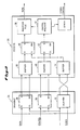
- FIG. 2 illustrates a general block diagram of the SCU to I/O interface. It should be recognized that while only a single transmitter 24 and receiver 26 are illustrated, both the SCU and the I/O include a transmitter and receiver to facilitate data transfer in each direction. Data contained in a D type flip flop 28 is delivered from the transmitter 24 over differential lines to a buffer 30 in the receiver 26. The clock signal for the flip flop 28 is provided by a source clock signal generated within the transmitter 24. To synchronize the transmitted data with the receiver hardware, the source clock signal is delivered from a buffer 32 over differential lines to a buffer 34 in the receiver 26. The receiver buffer 26, in turn, delivers the clock signal to the clock input of a D type flip flop 36 in the receiver 26.
- flip flops 28, 36 and buffer 30 While only a single set of flip flops 28, 36 and buffer 30 is illustrated, an additional seventeen of such sets are operated in parallel to allow the simultaneous transfer of a 2-byte word with 2-bit parity.
- the eighteen parallel flip flops 36 all deliver their outputs to a register file 38 where the data is maintained until the receiver specific logic acts to unload the register file and use the transmitted data.
- Handshaking between the two remote units is illustrated as initiating in the transmitter 24 from a source control with the actual signal being maintained in a D type flip flop 39.
- the transmitter clock signal is delivered to the clock input of the flip flop 39.
- Differential signals are delivered from the flip flop 39 to a buffer 40 in the receiver 26.
- the buffer 40 delivers the handshaking signal to a D type flip flop 42 which has its clock input connected to the buffer 34.
- the output of the flip flop 42 is connected to a control machine 44 which, in turn, passes signals to the register file 38.
- the handshaking signals have been reduced to a single set of differential lines communicating from the transmitter 24 to the receiver 26; however, the actual specific implementation includes four handshaking lines communicating in both directions.
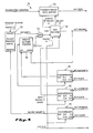
- FIGs. 3 and 4 there are shown detailed block diagrams of the transmitter and receiver control architecture, respectively.
- the discussion of FIGs. 3 and 4 should logically follow the flow of data and control signals between the two units.
- the data to be transmitted is provided by that unit which desires to send data to the other unit and is placed in the transmit packet data buffer 50. It is understood that either the I/O 18 or the SCU 20 can initiate data transfers in either direction; however, for ease of explanation it will be assumed here that the SCU 20 is sending data to the I/O 18. Accordingly, the SCU 20 places the packet of data in the buffer 50.
- the buffer 50 includes multiple storage locations separately identifiable with distinct packets of data. In other words, the buffer 50 actually consists of multiple buffers with an insert and remove pointer employed to store and access data at selected locations. Further, a packet of data consists of an indeterminate number of two-byte words.
- the receiver 26 includes a receive packet data buffer 51 similar in construction and number of buffers.
- a request to send the packet is delivered by the SCU 20 to a packet transmit queue 52.
- the queue 52 contains multiple storage locations with each queue storage location corresponding to one of the multiple buffers in the buffer 50. In this manner the queue 52 becomes a type of flag indicating to the transmitter 24, which of the buffers 50 contains data to be sent to the transmitter.
- the output of the queue 52 ultimately controls the delivery of data.
- a "not empty" signal is delivered to enable the buffer 50 to send the designated packet.
- the "not empty” signal is delivered to the input of an AND gate 54, thereby enabling the AND gate 54 to pass a signal from a receiver buffer counter 56.
- the receiver buffer counter 56 forms a portion of a means for the transmitter 24 to keep track of whether the receive packet data buffer 51 is full or not.
- This arrangement enhances the interface transfer speed.
- the alternative approach is to allow the receiver 26 to signal the transmitter 24 every time it is ready to receive a packet of data.
- the transmitter 26 must always wait before sending a packet of data.
- the transmitter 24 "knows" whether the receiver buffer 51 is full and does not need to wait. Rather, the transmitter 24 can continue to send packets with no delay.
- the receiver buffer counter 56 includes an increment and a decrement input.
- the decrement input is connected to the output of a transmit state machine 58, and in particular, to a transmit command available signal (XMT CMDAVAIL).
- the state machine 58 ultimately determines when the packet of data is sent and precedes the data with the XMT CMDAVAIL signal delivered to the receiver 26 and the counter 56.
- the counter 56 is initially set to a value equal to the number of buffers within the receive buffer 51. Thus, as each packet of data is transmitted to the receiver 26 the XMT CMDAVAIL signal decrements the counter 56 to indicate one less buffer is available. As long as the counter is not zero, the counter 56 supplies an enable signal through the AND gate 54 to the transmit state machine 58.
- the transmitter 24 and receiver 26 operate autonomously, such that, while the transmitter 24 is sending data to the receiver 26, the receiver 26 is unloading that data from the buffer and freeing those buffers to receive additional packets of data.
- a receiver buffer emptied signal (RCV BUFEMPTD) is delivered to the transmitter 24.
- This signal is synchronized with the transmitter clock via the synchronizer 60 and then delivered to the increment input of the receiver buffer counter 56. Therefore, as each receive buffer 51 is freed to receive additional data, the counter is incremented to indicate that an additional buffer is available. Thus, while the counter 56 is nonzero, the transmitter 24 continues to output packets of data without delay.
- the transmit state machine 58 also receives inputs from the transmit buffer 50 indicating the length of the packet. As discussed previously, bits 4 and 5 of the first two-byte word are encoded to indicate the length and are delivered to the transmit state machine 58. The state machine needs to "know" the length of the packet in order to "know” when to send the next packet of data. For example, four clock cycles are required to send an eight-byte packet. A two-byte word is sent during each clock cycle. Thus, by "knowing" that the packet requires four cycles, the state machine 58 can prepare to send the next packet on the fifth clock cycle.
- the state machine 58 delivers the XMT CMDAVAIL during the first clock cycle along with a select signal to the appropriate buffer of the transmit buffer 50. Thereafter, the transmit buffer 50 consecutively delivers each two-byte word over the sixteen-bit wide data interface.
- the receive buffer 51 receives each two-byte word and stores them in consecutive locations within a selected buffer.
- the parity and transmit clock signals are also delivered over the interface.
- the transmit clock signal enables the receive buffer 51 to synchronize the transmit data with the receive buffer 51.
- the parity of the received data is compared to the transmitted parity signals and any errors in parity are communicated to a receive state machine 62. A parity error ultimately results in the entire packet being retransmitted over the interface.
- a parity error detected by the receive buffer 51 is communicated to the receive state machine 62, which returns the signal to the transmitter 24 to initiate a retry on that packet of data.
- the bad parity signal from the state machine 62 is synchronized with the receive clock via synchronizer 64 and delivered to the transmitter 24 as a receive transfer retry signal (RCV XFERRETRY).
- a transmitter synchronizer 66 receives RCV XFERRETRY, synchronizes it with the transmitter clock, and delivers the signal to the transmit state machine 58.
- the state machine 58 responds by delivering XMT CMDAVAIL to the receiver and the buffer select signal to the same buffer as previously accessed. At the beginning of the next clock cycle, the transmit buffer 50 begins transmitting the packet of data again.
- the receiver 26 responds with a receive transfer acknowledge signal (RCV XFERACK) to indicate that the packet has been properly received and the transmitter 24 may safely remove that data transfer request from the queue 52.
- the receive state machine 62 receives a signal from the receive buffer 51 indicative of the length of the packet being transferred. As discussed previously, bits four and five of the first two-byte word are indicative of the packet length. These two bits are delivered to the state machine 62, so that at the end of the appropriate number of clock cycles, the transfer acknowledge signal is delivered. The signal is synchronized with the receive clock via synchronizer 68 and passed to the transmitter 24.
- a transmitter synchronizer 70 receives RCV XFERACK, synchronizes it with the transmit clock, and passes the signal to the packet transmit queue 52. In the queue 52, a valid bit is reset for that buffer and the remove pointer is incremented to indicate the next address.
- RCV XFERRETRY can also be initiated by the receiver specific logic.
- An OR gate 72 receives inputs from the synchronizer 62 and a receiver busy signal from the receiver specific logic. Thus, if for any reason the receiver unit (in this example, one of the I/O units) is unable or unwilling to receive the transmitted packet, it need only assert the receiver busy signal to generate RCV XFERRETRY. Further, it is desirable to block RCV XFERACK to prevent the receiver 26 from acknowledging the packet when the receiver busy signal is asserted.
- an AND gate 74 receives RCV XFERACK from the state machine 62 as one input. The second input to the AND gate 74 is the inverted receiver busy signal. Therefore, when the receiver busy signal is asserted, the AND gate 74 is not enabled to pass RCV XFERACK.
- the state machine 62 also provides a buffer available signal to the receiver specific logic to indicate when a packet receive is complete and in which buffer it is available.
- a synchronizer 76 synchronizes the buffer available signal with the receiver clock and passes that signal to the receiver specific logic. Thereafter, the receiver specific logic initiates an unload buffer signal to the receive buffer 51. The unload signal causes the buffer 51 to deliver the data contained in the designated buffer to the receiver specific logic.
- the counter 78 is configured to count between zero and the number of buffers in the receive buffer 51, such that, the output of the counter 78 acts as an insert pointer to the receive buffer 51.
- the increment input of the counter 78 receives its control signal from the XMT CMDAVAIL.
- the decrement input of the counter 78 receives its control signal from the receiver specific logic.
- the receiver specific logic When the receiver specific logic has successfully unloaded a buffer in the receive buffer 51, it generates a receive buffer emptied signal (RCV BUFEMPTD). This signal indicates that one of the buffers has been successfully unloaded and is now available to receive a new packet of data. As discussed previously, this same signal is supplied to the decrement input of the transmitter's receiver buffer counter 56. Accordingly, the counter 78 points to the next available buffer in the receive buffer 51.
- control begins at block 80 with the state machine 58 receiving the length of the packet from the transmit buffer 50.
- the length of the packet is significant in determining when the packet transfer is complete. For example, a packet that contains four two-byte words is finished transmitting at the beginning of the sixth clock cycle (one clock cycle for the XMT CMDAVAIL and one clock cycle for each two-byte word).
- the state machine 58 awaits the transmit packet signal from the AND gate 54. The absence of this signal indicates that either the receive buffer 51 is full or there is no data present in the transmit buffer 50 to be sent.
- Decision block 82 represents this portion of the state machine 58. As long as the transmit packet signal is not received, decision block 82 loops back on itself and does not allow control to proceed to the remainder of the function flow chart. Once the transmit packet signal is received, control transfers to block 84 where the actual transfer of data is initiated.
- the state machine 58 delivers XMT CMDAVAIL to the receiver 26. This signal informs the receiver 26 to begin monitoring the data lines at the next transmit clock signal.
- the state machine 58 delivers a select signal to the transmit buffer 50. This signal enables the selected buffer to begin unloading data in two-byte words beginning with the next transmit clock signal.
- XFERRETRY is monitored during the packet transfer to determine if the receiver 26 has detected any errors in the transmitted data.
- decision block 88 an asserted XFERRETRY causes control to return to block 84 where the transfer is attempted again. Otherwise, control passes to decision block 90 which acts to determine if the transfer is complete. Since the state machine knows the length of the packet and, consequently, the number of clock cycles required to transfer the packet, the completion of the transfer is simultaneous with the completion of the required number of clock cycles. Decision block 90 simply counts the number of clock cycles and returns control to decision block 88 if the requisite number of clock cycles has not yet occurred. This looping of control provides for periodic monitoring of the XFERRETRY signal. Upon completing the required number of clock cycles, the state machine 58 is freed to begin the process anew and send another packet of data.
- control begins at block 92 with the state machine 62 receiving the length of the packet from the transmit buffer 51. Once again, the length of the packet is significant in determining when the packet transfer is complete.
- decision block 94 the parity of each byte of data is compared to its corresponding parity bit generated by the transmit buffer 50 and delivered over the interface.
- decision block 96 transfers control back to decision block 94 to check the parity of the next two-bytes of data.
- the packet transfer is complete and successful. Accordingly, the buffer available signal is delivered to the receiver specific logic.
- the state machine 62 initiates XFERACK to the transmitter 24. The control process is complete and the state machine 62 is ready to receive the next packet of data.
- the synchronizers 64, 66, 68, 69, 70, 73, 76 have the same construction.
- the synchronizer 60 includes a series of five D type flip flops 110, 111, 112, 113, 114.
- the first flip flop 110 receives an input signal at its D input.
- the input signal is the signal which is to be synchronized with the clock signals.
- synchronizer 60 (see FIG. 3) receives, as its input, RCV BUFEMPTD which is to be synchronized with the transmit clock signal.
- the clock input to the flip flop 110 is the clock signal of the system which is generating the clock signal.
- the clock input to the synchronizer 60 is RCV CLOCK. This is provided to account for the skewing of the data and clock signals transmitted over the interface. It can be seen that since RCV BUFEMPTD is generated by the receiver 26 using RCV CLOCK and that both signals experience a similar delay from traversing the interface cable, then the value of RCV BUFEMPTD will be stable and valid at the RCV CLOCK transition.
- the Q output of the flip flop 110 is connected to the clock input of the flip flop 111.
- the D input of flip flop 111 is, however, connected to a logically high value.
- the flip flop 111 is clocked to pass the high signal through its Q output.
- the flip flop 111 also has a reset input which is used to set the value of its Q output from logically high to low.
- Each of the remaining flip flops 112, 113, 114 has its D input connected to the preceding flip flops Q output and its clock signal connected to the clock signal of the system to which the signal is to be synchronized.
- the synchronizer 60 has as its clock input, XMT CLOCK.
- the Q output of the final flip flop 114 serves as the output of the synchronizer while the not Q output is connected to the reset inputs of the flip flops 111, 112.
- Operation of the synchronizer begins with the input signal being stored in flip flop 110 coincident with the input clock signal.
- the synchronizer is intended to operate independently of the relative frequencies of the input and output clock signals.
- the operation of its internal flip flops are particularly sensitive to concurrent changes in the data and clock signals. Such a concurrent change produces unpredictable results from the flip flops, forcing the flip flops into a metastable state where their output is neither asserted nor unasserted.
- each flip flop stage of the synchronizer is increasing less likely to be forced into a metastable state.
- three stages are employed to give a probability that the final stage will attain a metastable state once in 107 years.
- the three stages synchronizer imposes a three cycle delay on all hand shaking signals delivered thereto. Accordingly, hand shaking signals can only be delivered at a rate of one-third of the output clock frequency.
- the Q110 output of the flip flop 110 is connected to a clock input of a flip flop 111.
- the D input of the flip flop 111 is connected to a logically high signal.
- a high data input and resulting Q110 transition from 0 to 1 causes the Q111 output to go high. That output is delivered to the first stage flip flop 112 of the three stages 112, 113, 114.
- the clock inputs to these three stages are controlled by the output clock signal.
- the high data signal will ripple through the three stages 112, 113, 114 in three output clock cycles and be delivered as an output of the synchronizer.
- the QN114 output of the final stage acts as a feedback signal to the flip flops 111, 112 to indicate that the data signal has been successfully synchronized with the output signal.
- the flip flops 111, 112 are reset by the low transition of the QN114 output in preparation of the next data signal.
- Flip flop 113 is not reset, so that the output of the synchronizer is at least two clock cycles in width. Since the flip flop 113 is not reset and it should be identical to the flip flop 114, its output will also ripple through the flip flop 114 on the fourth clock cycle.
- FIG. 8 the timing diagrams of the data and handshake signals for a simple single acknowledged packet are illustrated.
- the process begins with the transmit packet data buffer containing a 10-byte packet of data which it desires to send to its matching receiver. Accordingly, the transmit machine 58 delivers a XMT CMDAVAIL signal. The transmit machine 58 then delivers a "select N" signal to the transmit packet data buffer 50. Beginning immediately at the next clock cycle, the transmit packet data buffer 50 begins delivering the packet of data. 2-bytes of data are delivered in each of the five subsequent clock cycles until the transmit packet data buffer is emptied.
- the received control machine 62 checks for parity errors in the received packet of data and then assuming that the receiver was not busy, the RCV XFERACK signal is delivered to the transmitter.
- the RCV XFERACK signal is delivered to the packet transmit Queue 52 which removes the original request to send the packet N from the Queue 52.
- the receiver specific logic will deliver an UNLOAD BUFFER N signal to the receive packet data buffer 51 and remove that packet of data from the buffer 51.
- the receiver specific logic delivers a RCV BUFEMPTD signal to the transmitter.
- the RCV BUFEMPTD signal is used by the transmitter to increment the receive buffer counter 56, indicating that an additional buffer location is available in the receiver.
- the timing diagram for a simple single retried packet is illustrated. Like the simple single acknowledge packet the process begins with the transmitter receiving a request to send packet N into the packet transmit Queue 52.
- the transmit machine 58 delivers the transmit XMT CMDAVAIL signal and then selects the proper buffer in the transmit packet data buffer 50 from which to immediately begin sending the packet of data. In this case, however, owing either to the receiver being busy or a parity error occurring in the data transmission, the receiver delivers a RCV XFERRETRY signal to the transmitter. That RCV XFERRETRY signal is delivered to the transmit machine 58 indicating that packet N should be sent an additional time.
- the transmit machine 58 delivers the XMT CMDAVAIL signal and then selects the proper buffer in the transmit packet data buffer 50 to begin sending the packet of data.
- the transmit machine 58 sends another XMT CMDAVAIL signal to the receiver and then selects the other buffer in the transmit packet data buffer 50 to begin sending that packet of data.
- the receive control machine 62 initiates RCV XFERACK signals for both packet A and packet B causing the packet transmit Queue 52 to retire both requests to send packets of data.
- the receiver's specific logic will generate RCV BUFEMPTD signals for packets A and B to indicate to the receiver that both buffer locations in the receiver are free to receive additional packets of data.
- the timing diagrams of two back to back packets are sent, the first is retried, and the second is acknowledge.
- a XMT CMDAVAIL signal is delivered by the transmit machine 58 followed immediately by the packet of data for both of the selected packets A and B.
- the first handshaking signal returned by the receiver is the RCV XFERRETRY signal indicating that the first packet A has not been successfully received and should be retried.
- the second handshaking signal delivered by the receiver is, however, a RCV XFERACK signal indicating that packet B has been successfully received.
- the request to send packet B is removed from the packet transmit Queue 52 and the transmit machine 58 initiates a second transmission attempt for packet A.
- RCV BUFMEPTD signals are also returned from the receiver for both packet A and packet B thereby decrementing the counter 56 to indicate two additional buffer locations are available in the receiver.
Abstract
In the field of high speed digital computers it is common for the computer to be interfaced to a plurality of input/output (I/O) units. These I/O units allow the computer to interact with the external world and are typically purchased as off-the-shelf units. As the capabilities and speed of computers increase, so too must the rate of data transfer between the computer and its I/O units. This increased rate of transfer is effected without altering the physical connection to the I/O units by an interface having a transmitter (24) and a receiver (26) wherein the transmitter includes a counter which keeps track of the condition of a buffer in the receiver. The counter maintains a record of the number of packets of data sent to the receiver and the amount of remaining free buffer space. In this manner, the transmitter is free to continuously send data without waiting for permission to do so from the receiver.
Description
- This invention relates generally to an interface between functional components of a computer system and, more particularly, to an interface between a system control unit of a multi-processor computer system and its associated input/output (I/O) devices.
- In the field of computer systems, it is not unusual for a system to include a plurality of central processing units (CPUs) operating in parallel to enhance the system's speed of operation. Typically, each of the CPUs operate on a particular aspect of a single computer program and will, therefore, require access to the same program and variables stored in memory. It can be seen that each of the CPUs requires access to a shared common main memory, as well as input/output units (I/O). The I/O allows the computer system, in general, and the CPUs, in particular, to communicate with the external world. For example, the I/O includes such well known devices as disc and tape drives, communication devices, printers, plotters, workstations, etc.
- This parallel operation presents some problems in the form of access conflicts to the shared memory and I/O. A system control unit (SCU) is employed to manage these inter-unit communications. The SCU links the CPUs to the main memory and to the I/O through a series of independent interfaces. Data requests are received by the SCU from each of the units which, owing to the parallel nature of the CPU operation, occur at unscheduled times, and in particular, at the same time. These requests for data transfer are scheduled according to an arbitration algorithm and processed through the appropriate interface to/from the identified unit.
- Efficient communication between all system units ported into the SCU is critical to optimize parallel operation of the computer system. The speed of the interfaces is important to the overall operation of the computer system to ensure that a bottleneck of data does not develop. There is little point in individual units being able to operate at high speed if they must continually wait for data from other units.
- While the designers of such computer systems typically have control over the interfaces between each of the system units and can develop an interface capable of operating at the desired speed, this is not entirely true of the SCU to I/O interface. Rather, I/O devices are ordinarily of a standard design and construction and, in fact, are quite often purchased as off-the-shelf units from other manufacturers. Accordingly, the interface designer is constrained by the physical implementation of the I/O units. For example, one of the most significant design limitations is the physical number of communication lines. The limited number of communication lines has a direct impact on the speed at which data can be transferred.
- There are two methods to realize a desired rate of transfer. First, the width of the parallel interface can be increased to simply send more data during each clock cycle. However, in the instant case the designer has no control over the width of the interface since he is limited to the number of communication lines provided by the I/O unit. The second method involves increasing the speed of the clock so that more transfers can occur within the same duration of time. Of course, there are limitations as to how far the clock signal can be increased. There is a speed at which the hardware is simply incapable of operating.
- Further exacerbating this design limitation is the physical location of the I/O units. The I/O units are typically located remote from the SCU. The cable interconnecting the two units is subject to a harsh electromagnetic environment as it traverses multiple cabinets, each having a unique relative ground potential. Additionally, the high frequency clock system also contributes to electromagnetic interference. To contend with these noise problems and provide for data integrity, the interface typically employs noise reduction methods, such as differential communication. Unfortunately, these noise reduction methods further reduce the number of communication lines.
- Although noise immunity is improved by these methods, an occasional error will still occur. Therefore, some method of recognizing and communicating these errors must be provided. Accordingly, the limited number of communication lines is further reduced by the need for error communication.
- Traditionally, communication within a computing system is confined to relatively short distances (less than six feet). Accordingly, synchronous, parallel communication schemes are generally employed. This method of communication yields high bandwidths for the given technology and available number of wires. The length of interconnecting cables is usually limited by the system clock skew versus the propagation delay of the data path.
- Intermediate distance communication (less than 20 feet) is typically accomplished using a simple asynchronous parallel communication scheme. This method generally yields much longer transmission distances for a given technology and available number of wires, but with significantly lower bandwidths. Data transfer is commonly signaled with asynchronous strobe signals and the corresponding handshaking signals.
- Longer distance communication (greater than 20 feet) is generally accomplished with asynchronous, multidrop serial busses. Ethernet is exemplary of such a communication scheme.
- To provide an efficient, high-speed interface between a system control unit in a multi-processing system and various I/O units, the interface includes means for sequentially transmitting said packets of data between said system control unit and said input/output unit and means for sequentially receiving said packets of data transmitted between said system control unit and said input/output unit. The receiving means includes a buffer means for sequentially receiving and storing a plurality of said packets of data, means for controllably unloading packets of data from said receiving buffer means, and means for delivering a buffer emptied signal in response to a packet of data being unloaded from said receiving buffer means. The transmitting means includes means for calculating the number of packets of data stored in said receiving buffer means and delivering a signal responsive to the calculated number, and means for preventing said transmitting means from delivering additional packets of data in response to said calculated number being of a preselected magnitude.
- Other objects and advantages of the invention will become apparent upon reading the following detailed description and upon reference to the drawings in which:
- FIG. 1 is a block diagram of a computer system;
- FIG. 2 is a diagram of a SCU - I/O interface in the computer system of FIG. 1;
- FIG. 3 is a block diagram of transmitter control logic in the SCU - I/O interface;
- FIG. 4 is a block diagram of the receiver control logic in the SCU - I/O interface;
- FIG. 5 is a flowchart representation of the control scheme followed by a transmit state machine in the transmitter control logic of FIG. 3;
- FIG. 6 is a flowchart representation of the control scheme followed by a receive state machine in the receiver control logic of FIG. 4;
- FIG. 7 is a schematic diagram of a transmit or receive clock synchronizer;
- FIG. 8 is a timing diagram of the data and handshaking signals for a single acknowledged data packet transfer;
- FIG. 9 is a timing diagram of the data and handshaking signals for a single unacknowledged data packet transfer;
- FIG. 10 is a timing diagram of the data and handshaking signals for two consecutively acknowledged data packet transfers; and
- FIG. 11 is a timing diagram of the data and handshaking signals for two consecutive data packet transfers, where the first is acknowledged and the second is not.
- While the invention is susceptible to various modifications and alternative forms, specific embodiments thereof have been shown by way of example in the drawings and will herein be described in detail. It should be understood, however, that it is not intended to limit the invention to the particular forms disclosed, but on the contrary, the intention is to cover all modifications, equivalents, and alternatives falling within the spirit and scope of the invention as defined by the appended claims.
- Turning now to the drawings and referring first to FIG. 1, there is shown a block diagram of a
multi-processor computer system 10 which includes a plurality of central processing units (CPU1-CPU4) 11, 12, 13, 14. The CPUs require access to a shared commonmain memory 16, as well as, input/output units (I/O) 18. The I/O 18 allows thecomputer system 10, in general, and the CPUs, in particular, to communicate with the external world. For example, the I/O 18 includes such well known devices as disc and tape drives, communication devices, printers, plotters, workstations, etc. - To take full advantage of the multiple CPUs, the system is configured to allow CPU1-CPU4 to operate in parallel. This parallel operation presents some problems in the form of access conflicts to the shared
memory 16 and I/O 18. A system control unit (SCU) 20 is employed to manage these inter-unit communications. The SCU 20 links CPU1-CPU4 to themain memory 16 and to the I/O 18 through a series of independent interfaces. Data requests are received by the SCU 20 from each of the units which, owing to the parallel nature of the CPU operation, occur at unscheduled times, and in particular, at the same time. These requests for data transfer are scheduled according to an arbitration algorithm and processed through the appropriate interface to/from the identified unit. - The SCU 20 also links the various system units to a service processor unit (SPU) 22 which performs traditional console functions including status determination and the control of the overall operation of the processing system. In particular, the SCU 20 provides the
SPU 22 with means for communicating with the plurality of CPUs and provides access to all storage elements within the CPUs. - Efficient communication between all system units ported into the SCU 20 is critical to optimize parallel operation of the
computer system 10. While the designer ofsuch computer systems 10 typically has control over the interfaces between each of the system units, this is not entirely true of the SCU to I/O interface. Rather, I/O devices are ordinarily of a standard design and construction and, in fact, are quite often purchased as off-the-shelf units from other manufacturers. Accordingly, the interface designer is constrained by the physical implementation of the I/O units. For example, one of the most significant design limitations is the physical number of communication lines. In the present case the I/O devices are limited to 120 communication lines. - Further exacerbating this design limitation is the physical location of the I/O units. The I/O units are typically located remote from the SCU 20 and can be up to twelve feet distant. The cable interconnecting the two units is subject to a harsh electromagnetic environment as it traverses multiple cabinets, each having a unique relative ground potential. Additionally, the high frequency clock system (e.g. 500 MHz) also contributes to electromagnetic interference. To contend with these noise problems and provide for data integrity, the interface employs differential, series terminated ECL level signals. It should be noted that the use of series terminated ECL precludes the use of a single wire from communicating in two directions. That is, series terminated ECL allows signals to travel in only one direction on each wire. Thus, in order to transmit signals in both directions, twice as many lines are required.
- Unfortunately, these two methods of ensuring data integrity each reduce the number of communication lines by one-half. Accordingly, to provide a sufficient level of noise immunity, the number of communication lines is reduced from 120 to 30.
- Although noise immunity is improved by these two methods, an occasional error will still occur. Therefore, some method of recognizing and correcting these errors must be provided. Accordingly, parity signals are delivered along with the data. Further, in the event of a parity error, provision must be had for communicating the error back to the transmitter to allow the data to be communicated a second time. Thus, it can be seen that the limited number of communication lines is further reduced by the need for parity and some form of handshaking.
- Finally, owing to the great distance (12 feet) separating the SCU 20 and I/
O 18, the signals transmitted over the interface will experience a significant delay (e.g. 20 nsec for a 12 foot interface cable). This skewing of the transmitted data results in synchronization problems between the remote units. To solve this synchronization problem, the remote units each operate using an independent asynchronous clock signal and transmit their clock signal along with their data to the other remote unit. In this manner the clock signal and the data will be similarly affected by the transmission delay, so that using the delayed clock signal to enable the receiver latches eliminates the synchronization problem. Transmitting the clock signals does, however, further reduce the number of communication lines available for data transfer. - It should be appreciated that the present invention, though limited by 12 feet of cable and having only 120 transmission lines, has a raw communication speed of 125 megabytes/sec in each direction. Further, approximately 80 to 100 megabytes/sec of this raw speed consists of usable data. Moreover, it is also of interest to note that the clock cycle time is less than the cable delay (16 nsec versus 20 nsec). Accordingly, this means that two cycles of data are present on the twelve foot interface cable simultaneously.
- Further, the length of the interface cable is restricted according to the following formula:

LENGTH = cable length in inches;
TCYC = cycle time in picoseconds;
THLD = Hold time of the receive flip flop;
TSU = Set up time of the receive flip flop;
TSKI = Intrinsic skew of transmitter and receiver etch and SiO₂ in picoseconds;
TSKC = Skew contribution of cable in picoseconds/inch. - FIG. 2 illustrates a general block diagram of the SCU to I/O interface. It should be recognized that while only a
single transmitter 24 andreceiver 26 are illustrated, both the SCU and the I/O include a transmitter and receiver to facilitate data transfer in each direction. Data contained in a Dtype flip flop 28 is delivered from thetransmitter 24 over differential lines to abuffer 30 in thereceiver 26. The clock signal for theflip flop 28 is provided by a source clock signal generated within thetransmitter 24. To synchronize the transmitted data with the receiver hardware, the source clock signal is delivered from abuffer 32 over differential lines to abuffer 34 in thereceiver 26. Thereceiver buffer 26, in turn, delivers the clock signal to the clock input of a Dtype flip flop 36 in thereceiver 26. While only a single set offlip flops buffer 30 is illustrated, an additional seventeen of such sets are operated in parallel to allow the simultaneous transfer of a 2-byte word with 2-bit parity. The eighteenparallel flip flops 36 all deliver their outputs to aregister file 38 where the data is maintained until the receiver specific logic acts to unload the register file and use the transmitted data. - Handshaking between the two remote units is illustrated as initiating in the
transmitter 24 from a source control with the actual signal being maintained in a Dtype flip flop 39. The transmitter clock signal is delivered to the clock input of theflip flop 39. Differential signals are delivered from theflip flop 39 to abuffer 40 in thereceiver 26. Thebuffer 40 delivers the handshaking signal to a Dtype flip flop 42 which has its clock input connected to thebuffer 34. The output of theflip flop 42 is connected to acontrol machine 44 which, in turn, passes signals to theregister file 38. In this simplified block diagram, the handshaking signals have been reduced to a single set of differential lines communicating from thetransmitter 24 to thereceiver 26; however, the actual specific implementation includes four handshaking lines communicating in both directions. This specific implementation of the handshaking signals is discussed in greater detail in conjunction with the remaining specification. At this time it is sufficient to realize that thecontrol 44 responds to the handshaking signals to validate/invalidate the data contained in theregister file 38 and to initiate a retry on erroneous data. - Referring now simultaneously to FIGs. 3 and 4, there are shown detailed block diagrams of the transmitter and receiver control architecture, respectively. In view of the considerable interaction between the
transmitter 24 andreceiver 26, it is convenient to discuss the operation of each in light of the operation of the other. Accordingly, the discussion of FIGs. 3 and 4 should logically follow the flow of data and control signals between the two units. - The data to be transmitted is provided by that unit which desires to send data to the other unit and is placed in the transmit
packet data buffer 50. It is understood that either the I/O 18 or the SCU 20 can initiate data transfers in either direction; however, for ease of explanation it will be assumed here that the SCU 20 is sending data to the I/O 18. Accordingly, the SCU 20 places the packet of data in thebuffer 50. Thebuffer 50 includes multiple storage locations separately identifiable with distinct packets of data. In other words, thebuffer 50 actually consists of multiple buffers with an insert and remove pointer employed to store and access data at selected locations. Further, a packet of data consists of an indeterminate number of two-byte words. This is not to say that the length of the packet is unknown, merely that it may take on any desired length within a range of acceptable lengths. Bits four and five of the first two-byte word of data in the packet are encoded to contain information on the length of the packet. Similarly, thereceiver 26 includes a receivepacket data buffer 51 similar in construction and number of buffers. - At the same time, a request to send the packet is delivered by the SCU 20 to a packet transmit
queue 52. Like thebuffer 50, thequeue 52 contains multiple storage locations with each queue storage location corresponding to one of the multiple buffers in thebuffer 50. In this manner thequeue 52 becomes a type of flag indicating to thetransmitter 24, which of thebuffers 50 contains data to be sent to the transmitter. Thus, the output of thequeue 52 ultimately controls the delivery of data. As long as thequeue 52 contains a request to send a packet, a "not empty" signal is delivered to enable thebuffer 50 to send the designated packet. The "not empty" signal is delivered to the input of an ANDgate 54, thereby enabling the ANDgate 54 to pass a signal from areceiver buffer counter 56. - The receiver buffer counter 56 forms a portion of a means for the
transmitter 24 to keep track of whether the receivepacket data buffer 51 is full or not. This arrangement enhances the interface transfer speed. For example, the alternative approach is to allow thereceiver 26 to signal thetransmitter 24 every time it is ready to receive a packet of data. Thus, thetransmitter 26 must always wait before sending a packet of data. When one considers that the transmission time is significant (20 Nsec with only a 16 Nsec clock cycle), the delays become cumulative and performance of the interface is drastically reduced. However, in the instant implementation, thetransmitter 24 "knows" whether thereceiver buffer 51 is full and does not need to wait. Rather, thetransmitter 24 can continue to send packets with no delay. - The
receiver buffer counter 56 includes an increment and a decrement input. The decrement input is connected to the output of a transmitstate machine 58, and in particular, to a transmit command available signal (XMT CMDAVAIL). Thestate machine 58 ultimately determines when the packet of data is sent and precedes the data with the XMT CMDAVAIL signal delivered to thereceiver 26 and thecounter 56. Thecounter 56 is initially set to a value equal to the number of buffers within the receivebuffer 51. Thus, as each packet of data is transmitted to thereceiver 26 the XMT CMDAVAIL signal decrements thecounter 56 to indicate one less buffer is available. As long as the counter is not zero, thecounter 56 supplies an enable signal through the ANDgate 54 to the transmitstate machine 58. - It should be realized that the
transmitter 24 andreceiver 26 operate autonomously, such that, while thetransmitter 24 is sending data to thereceiver 26, thereceiver 26 is unloading that data from the buffer and freeing those buffers to receive additional packets of data. As thereceiver 26 retires data from thebuffer 51, a receiver buffer emptied signal (RCV BUFEMPTD) is delivered to thetransmitter 24. This signal is synchronized with the transmitter clock via thesynchronizer 60 and then delivered to the increment input of thereceiver buffer counter 56. Therefore, as each receivebuffer 51 is freed to receive additional data, the counter is incremented to indicate that an additional buffer is available. Thus, while thecounter 56 is nonzero, thetransmitter 24 continues to output packets of data without delay. - The transmit
state machine 58 also receives inputs from the transmitbuffer 50 indicating the length of the packet. As discussed previously, bits 4 and 5 of the first two-byte word are encoded to indicate the length and are delivered to the transmitstate machine 58. The state machine needs to "know" the length of the packet in order to "know" when to send the next packet of data. For example, four clock cycles are required to send an eight-byte packet. A two-byte word is sent during each clock cycle. Thus, by "knowing" that the packet requires four cycles, thestate machine 58 can prepare to send the next packet on the fifth clock cycle. - To initiate the transfer of data, the
state machine 58 delivers the XMT CMDAVAIL during the first clock cycle along with a select signal to the appropriate buffer of the transmitbuffer 50. Thereafter, the transmitbuffer 50 consecutively delivers each two-byte word over the sixteen-bit wide data interface. The receivebuffer 51 receives each two-byte word and stores them in consecutive locations within a selected buffer. At the same time, the parity and transmit clock signals are also delivered over the interface. The transmit clock signal enables the receivebuffer 51 to synchronize the transmit data with the receivebuffer 51. The parity of the received data is compared to the transmitted parity signals and any errors in parity are communicated to a receivestate machine 62. A parity error ultimately results in the entire packet being retransmitted over the interface. - A parity error detected by the receive
buffer 51 is communicated to the receivestate machine 62, which returns the signal to thetransmitter 24 to initiate a retry on that packet of data. The bad parity signal from thestate machine 62 is synchronized with the receive clock viasynchronizer 64 and delivered to thetransmitter 24 as a receive transfer retry signal (RCV XFERRETRY). Atransmitter synchronizer 66 receives RCV XFERRETRY, synchronizes it with the transmitter clock, and delivers the signal to the transmitstate machine 58. Thestate machine 58 responds by delivering XMT CMDAVAIL to the receiver and the buffer select signal to the same buffer as previously accessed. At the beginning of the next clock cycle, the transmitbuffer 50 begins transmitting the packet of data again. - Alternatively, if no parity error is detected, then the
receiver 26 responds with a receive transfer acknowledge signal (RCV XFERACK) to indicate that the packet has been properly received and thetransmitter 24 may safely remove that data transfer request from thequeue 52. The receivestate machine 62 receives a signal from the receivebuffer 51 indicative of the length of the packet being transferred. As discussed previously, bits four and five of the first two-byte word are indicative of the packet length. These two bits are delivered to thestate machine 62, so that at the end of the appropriate number of clock cycles, the transfer acknowledge signal is delivered. The signal is synchronized with the receive clock viasynchronizer 68 and passed to thetransmitter 24. Atransmitter synchronizer 70 receives RCV XFERACK, synchronizes it with the transmit clock, and passes the signal to the packet transmitqueue 52. In thequeue 52, a valid bit is reset for that buffer and the remove pointer is incremented to indicate the next address. - It should be noted that RCV XFERRETRY can also be initiated by the receiver specific logic. An OR gate 72 receives inputs from the
synchronizer 62 and a receiver busy signal from the receiver specific logic. Thus, if for any reason the receiver unit (in this example, one of the I/O units) is unable or unwilling to receive the transmitted packet, it need only assert the receiver busy signal to generate RCV XFERRETRY. Further, it is desirable to block RCV XFERACK to prevent thereceiver 26 from acknowledging the packet when the receiver busy signal is asserted. Thus, an ANDgate 74 receives RCV XFERACK from thestate machine 62 as one input. The second input to the ANDgate 74 is the inverted receiver busy signal. Therefore, when the receiver busy signal is asserted, the ANDgate 74 is not enabled to pass RCV XFERACK. - The
state machine 62 also provides a buffer available signal to the receiver specific logic to indicate when a packet receive is complete and in which buffer it is available. Asynchronizer 76 synchronizes the buffer available signal with the receiver clock and passes that signal to the receiver specific logic. Thereafter, the receiver specific logic initiates an unload buffer signal to the receivebuffer 51. The unload signal causes thebuffer 51 to deliver the data contained in the designated buffer to the receiver specific logic. - Loading of the receive
buffer 51 is controlled by a receivebuffer counter 78. Thecounter 78 is configured to count between zero and the number of buffers in the receivebuffer 51, such that, the output of thecounter 78 acts as an insert pointer to the receivebuffer 51. The increment input of thecounter 78 receives its control signal from the XMT CMDAVAIL. Conversely, the decrement input of thecounter 78 receives its control signal from the receiver specific logic. When the receiver specific logic has successfully unloaded a buffer in the receivebuffer 51, it generates a receive buffer emptied signal (RCV BUFEMPTD). This signal indicates that one of the buffers has been successfully unloaded and is now available to receive a new packet of data. As discussed previously, this same signal is supplied to the decrement input of the transmitter'sreceiver buffer counter 56. Accordingly, thecounter 78 points to the next available buffer in the receivebuffer 51. - Operation of the transmit and receive
state machines state machine 58 functional flow chart is illustrated, control begins atblock 80 with thestate machine 58 receiving the length of the packet from the transmitbuffer 50. The length of the packet is significant in determining when the packet transfer is complete. For example, a packet that contains four two-byte words is finished transmitting at the beginning of the sixth clock cycle (one clock cycle for the XMT CMDAVAIL and one clock cycle for each two-byte word). - Thereafter, the
state machine 58 awaits the transmit packet signal from the ANDgate 54. The absence of this signal indicates that either the receivebuffer 51 is full or there is no data present in the transmitbuffer 50 to be sent.Decision block 82 represents this portion of thestate machine 58. As long as the transmit packet signal is not received, decision block 82 loops back on itself and does not allow control to proceed to the remainder of the function flow chart. Once the transmit packet signal is received, control transfers to block 84 where the actual transfer of data is initiated. Thestate machine 58 delivers XMT CMDAVAIL to thereceiver 26. This signal informs thereceiver 26 to begin monitoring the data lines at the next transmit clock signal. - In
block 86, thestate machine 58 delivers a select signal to the transmitbuffer 50. This signal enables the selected buffer to begin unloading data in two-byte words beginning with the next transmit clock signal. - XFERRETRY is monitored during the packet transfer to determine if the
receiver 26 has detected any errors in the transmitted data. Indecision block 88, an asserted XFERRETRY causes control to return to block 84 where the transfer is attempted again. Otherwise, control passes todecision block 90 which acts to determine if the transfer is complete. Since the state machine knows the length of the packet and, consequently, the number of clock cycles required to transfer the packet, the completion of the transfer is simultaneous with the completion of the required number of clock cycles.Decision block 90 simply counts the number of clock cycles and returns control todecision block 88 if the requisite number of clock cycles has not yet occurred. This looping of control provides for periodic monitoring of the XFERRETRY signal. Upon completing the required number of clock cycles, thestate machine 58 is freed to begin the process anew and send another packet of data. - Referring now to FIG. 6, wherein the receive
state machine 62 functional flowchart is illustrated, control begins atblock 92 with thestate machine 62 receiving the length of the packet from the transmitbuffer 51. Once again, the length of the packet is significant in determining when the packet transfer is complete. - Control loops through decision blocks 94, 96 as each two-byte word of data is received. In
decision block 94, the parity of each byte of data is compared to its corresponding parity bit generated by the transmitbuffer 50 and delivered over the interface. As long as no parity errors are detected and all of the data has not been received,decision block 96 transfers control back todecision block 94 to check the parity of the next two-bytes of data. In the event of a parity error, control transfers to block 98 where thestate machine 62 initiates XFERRETRY to thetransmitter 24. - Alternatively, at the end of the requisite number of clock cycles without a parity error, control transfers to block 100. At this point, the packet transfer is complete and successful. Accordingly, the buffer available signal is delivered to the receiver specific logic. Similarly, in
block 102 thestate machine 62 initiates XFERACK to thetransmitter 24. The control process is complete and thestate machine 62 is ready to receive the next packet of data. - Referring now to FIG. 7, a general schematic diagram of the
synchronizer 60 is illustrated. Thesynchronizers synchronizer 60 includes a series of five Dtype flip flops first flip flop 110 receives an input signal at its D input. The input signal is the signal which is to be synchronized with the clock signals. For example, synchronizer 60 (see FIG. 3) receives, as its input, RCV BUFEMPTD which is to be synchronized with the transmit clock signal. - The clock input to the
flip flop 110 is the clock signal of the system which is generating the clock signal. For example, the clock input to thesynchronizer 60 is RCV CLOCK. This is provided to account for the skewing of the data and clock signals transmitted over the interface. It can be seen that since RCV BUFEMPTD is generated by thereceiver 26 using RCV CLOCK and that both signals experience a similar delay from traversing the interface cable, then the value of RCV BUFEMPTD will be stable and valid at the RCV CLOCK transition. - The Q output of the
flip flop 110 is connected to the clock input of theflip flop 111. The D input offlip flop 111 is, however, connected to a logically high value. Thus, when the input to flipflop 110 changes states, theflip flop 111 is clocked to pass the high signal through its Q output. Theflip flop 111 also has a reset input which is used to set the value of its Q output from logically high to low. - Each of the remaining
flip flops synchronizer 60 has as its clock input, XMT CLOCK. The Q output of thefinal flip flop 114 serves as the output of the synchronizer while the not Q output is connected to the reset inputs of theflip flops - Operation of the synchronizer begins with the input signal being stored in
flip flop 110 coincident with the input clock signal. The synchronizer is intended to operate independently of the relative frequencies of the input and output clock signals. However, it should be appreciated that the operation of its internal flip flops are particularly sensitive to concurrent changes in the data and clock signals. Such a concurrent change produces unpredictable results from the flip flops, forcing the flip flops into a metastable state where their output is neither asserted nor unasserted. - Therefore, in order to avoid ultimately delivering an output from the synchronizer which is metastable, multiple stages of sequential flip flops are employed. Each flip flop stage of the synchronizer is increasing less likely to be forced into a metastable state. Preferably, three stages are employed to give a probability that the final stage will attain a metastable state once in 10⁷ years.
- The three stages synchronizer imposes a three cycle delay on all hand shaking signals delivered thereto. Accordingly, hand shaking signals can only be delivered at a rate of one-third of the output clock frequency.
- The Q₁₁₀ output of the
flip flop 110 is connected to a clock input of aflip flop 111. The D input of theflip flop 111 is connected to a logically high signal. Thus, a high data input and resulting Q₁₁₀ transition from 0 to 1 causes the Q₁₁₁ output to go high. That output is delivered to the firststage flip flop 112 of the threestages - Assuming that the data and clock transitions are not concurrent, the high data signal will ripple through the three
stages flip flops flip flops Flip flop 113 is not reset, so that the output of the synchronizer is at least two clock cycles in width. Since theflip flop 113 is not reset and it should be identical to theflip flop 114, its output will also ripple through theflip flop 114 on the fourth clock cycle. - It can be seen that if the data input to the
flip flop 110 is a low value, then the Q₁₁₀ output remains low and does not clock theflip flop 111. Accordingly, since theflip flop 111 was previously reset, its output is low, thereby matching the data input. Like the high data input, this low data input ripples through the three stages offlip flops - Operation of the interface may best be described by way of example. Referring now to FIG. 8, the timing diagrams of the data and handshake signals for a simple single acknowledged packet are illustrated. The process begins with the transmit packet data buffer containing a 10-byte packet of data which it desires to send to its matching receiver. Accordingly, the transmit
machine 58 delivers a XMT CMDAVAIL signal. The transmitmachine 58 then delivers a "select N" signal to the transmitpacket data buffer 50. Beginning immediately at the next clock cycle, the transmitpacket data buffer 50 begins delivering the packet of data. 2-bytes of data are delivered in each of the five subsequent clock cycles until the transmit packet data buffer is emptied. The receivedcontrol machine 62 checks for parity errors in the received packet of data and then assuming that the receiver was not busy, the RCV XFERACK signal is delivered to the transmitter. The RCV XFERACK signal is delivered to the packet transmitQueue 52 which removes the original request to send the packet N from theQueue 52. Thereafter, the receiver specific logic will deliver an UNLOAD BUFFER N signal to the receivepacket data buffer 51 and remove that packet of data from thebuffer 51. Once thebuffer 51 is empty, the receiver specific logic delivers a RCV BUFEMPTD signal to the transmitter. The RCV BUFEMPTD signal is used by the transmitter to increment the receivebuffer counter 56, indicating that an additional buffer location is available in the receiver. - Referring now to FIG. 9, the timing diagram for a simple single retried packet is illustrated. Like the simple single acknowledge packet the process begins with the transmitter receiving a request to send packet N into the packet transmit
Queue 52. The transmitmachine 58 delivers the transmit XMT CMDAVAIL signal and then selects the proper buffer in the transmitpacket data buffer 50 from which to immediately begin sending the packet of data. In this case, however, owing either to the receiver being busy or a parity error occurring in the data transmission, the receiver delivers a RCV XFERRETRY signal to the transmitter. That RCV XFERRETRY signal is delivered to the transmitmachine 58 indicating that packet N should be sent an additional time. - Referring now to FIG. 10, the timing diagrams of two back to back packets are sent and both are acknowledged. The transmit
machine 58 delivers the XMT CMDAVAIL signal and then selects the proper buffer in the transmitpacket data buffer 50 to begin sending the packet of data. After the first packet of data has been sent to the receiver, the transmitmachine 58 sends another XMT CMDAVAIL signal to the receiver and then selects the other buffer in the transmitpacket data buffer 50 to begin sending that packet of data. Subsequently, the receivecontrol machine 62 initiates RCV XFERACK signals for both packet A and packet B causing the packet transmitQueue 52 to retire both requests to send packets of data. Similarly, the receiver's specific logic will generate RCV BUFEMPTD signals for packets A and B to indicate to the receiver that both buffer locations in the receiver are free to receive additional packets of data. - Referring now to FIG. 11, the timing diagrams of two back to back packets are sent, the first is retried, and the second is acknowledge. Like the timing diagrams of FIG. 10, a XMT CMDAVAIL signal is delivered by the transmit
machine 58 followed immediately by the packet of data for both of the selected packets A and B. Thereafter, the first handshaking signal returned by the receiver is the RCV XFERRETRY signal indicating that the first packet A has not been successfully received and should be retried. The second handshaking signal delivered by the receiver is, however, a RCV XFERACK signal indicating that packet B has been successfully received. Thus, the request to send packet B is removed from the packet transmitQueue 52 and the transmitmachine 58 initiates a second transmission attempt for packet A. RCV BUFMEPTD signals are also returned from the receiver for both packet A and packet B thereby decrementing thecounter 56 to indicate two additional buffer locations are available in the receiver.
Claims (20)
1. An interface for controlling the flow of data between a system control unit and an input/output unit, comprising: means (24) for sequentially transmitting packets of data and means (26) for sequentially receiving the packets; characterised in that:
(1) the receiving means (26) includes receiving buffer means (51) for sequentially receiving and storing a plurality of packets of data; means (62) for controllably unloading packets of data from the receiving buffer means (51); and means for delivering a buffer emptied signal in response to a packet of data being unloaded from the receiving buffer means; further characterised in that:
(2) the transmitting means (24) includes means (56) for determining the number of packets of data stored in the receiving buffer means (51) and delivering a signal representative of the said number; and means (58) for preventing the transmitting means (24) from delivering additional packets of data in response to the said number being of a certain magnitude.
2. An interface, as set forth in Claim 1, wherein the transmitting means (24) includes means (58) for calculating a parity signal representative of the transmitted data and delivering the parity signal to the receiving means (26).
3. An interface, as set forth in Claim 2, wherein the receiving means (26) includes means (62) for receiving the parity signal, determining the parity of the received data, comparing the received parity signal with the determined parity signal, delivering a retry signal to the transmitting means (24) in response to the determined and received parities being inconsistent, and delivering an acknowledge signal in response to the determined and received parities being consistent.
4. An interface, as set forth in Claim 3, wherein the transmitting means includes means (66, 58) for receiving the retry signal and restarting the transfer of the packet of data corresponding to the retry signal.
5. An interface, as set forth in Claim 3, wherein the transmitting means (24) includes means (78) for receiving the acknowledge signal and retiring the packet of data corresponding to the acknowledge signal.
6. An interface, as set forth in any one of the preceding claims wherein the transmitting means (24) includes means for generating a first periodic clock signal to synchronise the operation of the transmitting means, and means for delivering the first clock signal to the receiving means (26).
7. An interface, as set forth in Claim 6, wherein the receiving means (26) includes means for generating a second periodic clock signal, asynchronous with the first periodic clock signal, to synchronise the operation of the receiving means, and means for delivering the second clock signal to the transmitting means.
8. An interface, as set forth in Claim 1, wherein the transmitting means (24) includes means for delivering a command available signal during a first periodic clock signal prior to delivering a packet of data.
9. An interface, as set forth in Claim 8, wherein the receiving means (26) includes means for receiving the command available signal and incrementing an insert pointer to the receiving buffer means (51) in response to receiving the command available signal.
10. An interface, as set forth in Claim 8, wherein the means for determining the number of packets of data stored in the receiving buffer means receives the command available signal and decrements the said number.
11. An interface, as set forth in Claim 3, wherein the means for determining the number of packets of data stored in the receiving buffer (51) means receives the buffer emptied signal and increments the said number.
12. A method for controlling the flow of data in a computer system, the method being characterised by: sequentially transmitting packets of data; sequentially receiving the packets and storing them in a receiving buffer; controllably unloading packets of data from the receiving buffer; delivering a buffer emptied signal in response to a packet of data being unloaded from the receiving buffer; determining the number of packets of data stored in the receiving buffer; and selectively inhibiting the transmitting of additional packets of data in response to the said number being of a certain magnitude.
13. A method, as set forth in Claim 12, further comprising calculating a parity signal responsive to the transmitted data and transmitting the parity signal along with the packets of data.
14. A method, as set forth in Claim 13, further comprising receiving the parity signal determining the parity of the received data, comparing the received parity with the determined parity, returning a retry signal in response to the determined and received parities being inconsistent, and returning an acknowledge signal in response to the determined and received parities being consistent.
15. A method, as set forth in Claim 14, further comprising receiving the retry signal and restarting the transmission of the packet of data corresponding to the retry signal.
16. A method, as set forth in Claim 14, further comprising receiving the acknowledge signal and retiring the packet of data corresponding to the acknowledge signal.
17. A method, as set forth in Claim 12, further comprising generating a first periodic clock signal to synchronise the transmitting of data packets, and delivering the first clock signal to enable the receiving buffer to receive the transmitted data.
18. A method, as set forth in Claim 17, further comprising generating a second periodic clock signal, asynchronous with the first periodic clock signal, to synchronise the receiving of the packets of data, and delivering the second clock signal along with the buffer emptied signal.
19. A method, as set forth in Claim 12, further comprising transmitting a command available signal during a first periodic clock signal prior to transmitting a packet of data.
20. A method, as set forth in Claim 12, in which the determining of the number of packets of data stored in the receiving buffer is effected by incrementing the determined number in response to receiving the buffer emptied signal and decrementing the determined number for each transmission of one of the packets of data.
Applications Claiming Priority (2)
| Application Number | Priority Date | Filing Date | Title |
|---|---|---|---|
| US306862 | 1989-02-03 | ||
| US07/306,862 US4965793A (en) | 1989-02-03 | 1989-02-03 | Method and apparatus for interfacing a system control unit for a multi-processor |
Publications (2)
| Publication Number | Publication Date |
|---|---|
| EP0380856A2 true EP0380856A2 (en) | 1990-08-08 |
| EP0380856A3 EP0380856A3 (en) | 1992-01-29 |
Family
ID=23187200
Family Applications (1)
| Application Number | Title | Priority Date | Filing Date |
|---|---|---|---|
| EP19890309386 Withdrawn EP0380856A3 (en) | 1989-02-03 | 1989-09-15 | Method and apparatus for interfacing a system control unit for a multi-processor |
Country Status (5)
| Country | Link |
|---|---|
| US (1) | US4965793A (en) |
| EP (1) | EP0380856A3 (en) |
| JP (1) | JPH065519B2 (en) |
| AU (1) | AU628532B2 (en) |
| CA (1) | CA1325286C (en) |
Cited By (7)
| Publication number | Priority date | Publication date | Assignee | Title |
|---|---|---|---|---|
| AU652371B2 (en) * | 1990-06-29 | 1994-08-25 | Fujitsu Limited | Data transfer system |
| EP0646871A2 (en) * | 1993-10-05 | 1995-04-05 | Hitachi, Ltd. | Data transfer control system |
| EP0751465A1 (en) * | 1995-06-30 | 1997-01-02 | Bull S.A. | Apparatus for the exchange of messages between two computers and method of command execution using the apparatus |
| WO1997031459A1 (en) * | 1996-02-22 | 1997-08-28 | Hal Computer Systems, Inc. | Flow control protocol system and method |
| US5991296A (en) * | 1996-02-22 | 1999-11-23 | Fujitsu, Ltd. | Crossbar switch and method with reduced voltage swing and no internal blocking data path |
| FR2884035A1 (en) * | 2005-04-04 | 2006-10-06 | St Microelectronics Sa | System on chip for forming complex circuit on silicon chip, has transmitter circuit with data bus connecting receiver circuit`s input port to transmitter circuit`s output port, and two links connecting terminals of circuits |
| EP0823167B1 (en) * | 1996-02-22 | 2008-07-02 | Fujitsu Limited | Method and apparatus for coordinating access to an output of a routing device in a packet switching network |
Families Citing this family (34)
| Publication number | Priority date | Publication date | Assignee | Title |
|---|---|---|---|---|
| WO1991009366A1 (en) * | 1989-12-19 | 1991-06-27 | E-Systems, Incorporated | Method and apparatus for dispersed end-entity flow control in computer networks |
| JPH03225429A (en) * | 1990-01-30 | 1991-10-04 | Sharp Corp | Integrated circuit device |
| US5175727A (en) * | 1990-04-16 | 1992-12-29 | Maher John W | Communication system network interconnecting a plurality of communication systems |
| US5130986A (en) * | 1990-04-27 | 1992-07-14 | At&T Bell Laboratories | High speed transport protocol with two windows |
| JPH077975B2 (en) * | 1990-08-20 | 1995-01-30 | インターナショナル・ビジネス・マシーンズ・コーポレイション | System and method for controlling data transmission |
| US5132967A (en) * | 1990-10-29 | 1992-07-21 | International Business Machines Corporation | Single competitor arbitration scheme for common bus |
| US5226121A (en) * | 1990-11-19 | 1993-07-06 | Ag Communication Systems Corporation | Method of bit rate de-adaption using the ECMA 102 protocol |
| US5555438A (en) * | 1991-07-24 | 1996-09-10 | Allen-Bradley Company, Inc. | Method for synchronously transferring serial data to and from an input/output (I/O) module with true and complement error detection coding |
| JP2834927B2 (en) * | 1992-02-28 | 1998-12-14 | 三菱電機株式会社 | Computer system |
| US6157967A (en) * | 1992-12-17 | 2000-12-05 | Tandem Computer Incorporated | Method of data communication flow control in a data processing system using busy/ready commands |
| US6233702B1 (en) * | 1992-12-17 | 2001-05-15 | Compaq Computer Corporation | Self-checked, lock step processor pairs |
| US5664104A (en) * | 1992-12-18 | 1997-09-02 | Fujitsu Limited | Transfer processor including a plurality of failure display units wherein a transfer process is prohibited if failure is indicated in a failure display unit |
| US5604866A (en) * | 1993-09-30 | 1997-02-18 | Silicon Graphics, Inc. | Flow control system having a counter in transmitter for decrementing and incrementing based upon transmitting and received message size respectively for indicating free space in receiver |
| US5581705A (en) * | 1993-12-13 | 1996-12-03 | Cray Research, Inc. | Messaging facility with hardware tail pointer and software implemented head pointer message queue for distributed memory massively parallel processing system |
| US5602848A (en) * | 1995-06-05 | 1997-02-11 | International Business Machines Corporation | Multi-mode TDM interface circuit |
| US5841973A (en) * | 1996-03-13 | 1998-11-24 | Cray Research, Inc. | Messaging in distributed memory multiprocessing system having shell circuitry for atomic control of message storage queue's tail pointer structure in local memory |
| US5864738A (en) * | 1996-03-13 | 1999-01-26 | Cray Research, Inc. | Massively parallel processing system using two data paths: one connecting router circuit to the interconnect network and the other connecting router circuit to I/O controller |
| JPH1051514A (en) * | 1996-07-30 | 1998-02-20 | Oki Electric Ind Co Ltd | Interface device |
| US6209072B1 (en) * | 1997-05-06 | 2001-03-27 | Intel Corporation | Source synchronous interface between master and slave using a deskew latch |
| KR100280817B1 (en) * | 1997-12-03 | 2001-02-01 | 정선종 | Data transmission protocol and its control method point-to-point connetion in inter connetion network |
| US6128672A (en) * | 1998-03-10 | 2000-10-03 | Motorola, Inc. | Data transfer using software interrupt service routine between host processor and external device with queue of host processor and hardware queue pointers on external device |
| JP3592547B2 (en) | 1998-09-04 | 2004-11-24 | 株式会社ルネサステクノロジ | Information processing apparatus and signal transfer method |
| US6665807B1 (en) * | 1998-09-04 | 2003-12-16 | Hitachi, Ltd. | Information processing apparatus |
| US6216174B1 (en) | 1998-09-29 | 2001-04-10 | Silicon Graphics, Inc. | System and method for fast barrier synchronization |
| US6597692B1 (en) | 1999-04-21 | 2003-07-22 | Hewlett-Packard Development, L.P. | Scalable, re-configurable crossbar switch architecture for multi-processor system interconnection networks |
| US6378029B1 (en) | 1999-04-21 | 2002-04-23 | Hewlett-Packard Company | Scalable system control unit for distributed shared memory multi-processor systems |
| US6263415B1 (en) | 1999-04-21 | 2001-07-17 | Hewlett-Packard Co | Backup redundant routing system crossbar switch architecture for multi-processor system interconnection networks |
| KR20020031378A (en) * | 1999-07-06 | 2002-05-01 | 다니구찌 이찌로오, 기타오카 다카시 | Drive control system |
| US6298394B1 (en) * | 1999-10-01 | 2001-10-02 | Stmicroelectronics, Ltd. | System and method for capturing information on an interconnect in an integrated circuit |
| US6813275B1 (en) * | 2000-04-21 | 2004-11-02 | Hewlett-Packard Development Company, L.P. | Method and apparatus for preventing underflow and overflow across an asynchronous channel |
| US6910062B2 (en) * | 2001-07-31 | 2005-06-21 | International Business Machines Corporation | Method and apparatus for transmitting packets within a symmetric multiprocessor system |
| US6732207B2 (en) * | 2001-07-31 | 2004-05-04 | Pri Automation, Inc. | Fast serial interface used for controller to robot communications |
| JP2003177992A (en) * | 2001-12-10 | 2003-06-27 | Seiko Epson Corp | Differential communication system, differential communication equipment, differential communication program and differential communication method |
| US20050262311A1 (en) * | 2004-05-20 | 2005-11-24 | Lippincott Louis A | Hierarchical processor architecture for video processing |
Citations (5)
| Publication number | Priority date | Publication date | Assignee | Title |
|---|---|---|---|---|
| EP0077008A2 (en) * | 1981-10-05 | 1983-04-20 | Digital Equipment Corporation | Interface apparatus in a data processing system |
| US4392200A (en) * | 1980-01-28 | 1983-07-05 | Digital Equipment Corporation | Cached multiprocessor system with pipeline timing |
| EP0225024A2 (en) * | 1985-11-23 | 1987-06-10 | International Computers Limited | Data transmission system |
| EP0242634A2 (en) * | 1986-04-22 | 1987-10-28 | International Business Machines Corporation | Byte count handling in serial channel extender with buffering for data pre-fetch |
| EP0249116A2 (en) * | 1986-06-02 | 1987-12-16 | Hitachi, Ltd. | Method for controlling data transfer buffer |
Family Cites Families (10)
| Publication number | Priority date | Publication date | Assignee | Title |
|---|---|---|---|---|
| ZA83892B (en) * | 1982-02-19 | 1983-11-30 | Int Computers Ltd | Data transmission systems |
| IT1155644B (en) * | 1982-03-17 | 1987-01-28 | Cselt Centro Studi Lab Telecom | INTERFACE TO ACCESS A WIDEBAND BUS FOR INTEGRATED TRAFFIC DATA PHONE |
| US4500958A (en) * | 1982-04-21 | 1985-02-19 | Digital Equipment Corporation | Memory controller with data rotation arrangement |
| US4667287A (en) * | 1982-10-28 | 1987-05-19 | Tandem Computers Incorporated | Multiprocessor multisystem communications network |
| US4543626A (en) * | 1982-12-06 | 1985-09-24 | Digital Equipment Corporation | Apparatus and method for controlling digital data processing system employing multiple processors |
| US4543628A (en) * | 1983-01-28 | 1985-09-24 | Digital Equipment Corporation | Bus for data processing system with fault cycle operation |
| US4730308A (en) * | 1985-10-04 | 1988-03-08 | International Business Machines Corporation | Interface between a computer bus and a serial packet link |
| DE3686629T2 (en) * | 1985-10-07 | 1993-03-18 | Nec Corp | HIGH SPEED PACKAGE SWITCHING SYSTEM WITH CONTINUOUS FLOW CONTROL AND REPEAT RETRY. |
| GB8605613D0 (en) * | 1986-03-07 | 1986-04-16 | Limb J O | Traffic scheduler |
| US4823312A (en) * | 1986-10-30 | 1989-04-18 | National Semiconductor Corp. | Asynchronous communications element |
-
1989
- 1989-02-03 US US07/306,862 patent/US4965793A/en not_active Expired - Lifetime
- 1989-09-15 EP EP19890309386 patent/EP0380856A3/en not_active Withdrawn
- 1989-09-19 CA CA000611907A patent/CA1325286C/en not_active Expired - Fee Related
- 1989-11-29 JP JP1310482A patent/JPH065519B2/en not_active Expired - Lifetime
-
1990
- 1990-04-27 AU AU53953/90A patent/AU628532B2/en not_active Ceased
Patent Citations (5)
| Publication number | Priority date | Publication date | Assignee | Title |
|---|---|---|---|---|
| US4392200A (en) * | 1980-01-28 | 1983-07-05 | Digital Equipment Corporation | Cached multiprocessor system with pipeline timing |
| EP0077008A2 (en) * | 1981-10-05 | 1983-04-20 | Digital Equipment Corporation | Interface apparatus in a data processing system |
| EP0225024A2 (en) * | 1985-11-23 | 1987-06-10 | International Computers Limited | Data transmission system |
| EP0242634A2 (en) * | 1986-04-22 | 1987-10-28 | International Business Machines Corporation | Byte count handling in serial channel extender with buffering for data pre-fetch |
| EP0249116A2 (en) * | 1986-06-02 | 1987-12-16 | Hitachi, Ltd. | Method for controlling data transfer buffer |
Cited By (14)
| Publication number | Priority date | Publication date | Assignee | Title |
|---|---|---|---|---|
| AU652371B2 (en) * | 1990-06-29 | 1994-08-25 | Fujitsu Limited | Data transfer system |
| EP0646871A2 (en) * | 1993-10-05 | 1995-04-05 | Hitachi, Ltd. | Data transfer control system |
| EP0646871A3 (en) * | 1993-10-05 | 1996-07-31 | Hitachi Ltd | Data transfer control system. |
| US5623607A (en) * | 1993-10-05 | 1997-04-22 | Hitachi, Ltd. | Data transfer control method for controlling transfer of data through a buffer without causing the buffer to become empty or overflow |
| US5928326A (en) * | 1995-06-30 | 1999-07-27 | Bull S.A. | Programmable, multi-buffer device and method for exchanging messages between peer-to-peer network nodes |
| EP0751465A1 (en) * | 1995-06-30 | 1997-01-02 | Bull S.A. | Apparatus for the exchange of messages between two computers and method of command execution using the apparatus |
| FR2736176A1 (en) * | 1995-06-30 | 1997-01-03 | Bull Sa | DEVICE FOR EXCHANGING MESSAGES BETWEEN TWO COMPUTER MACHINES AND METHOD FOR PERFORMING CONTROLS USING THE DEVICE |
| WO1997031459A1 (en) * | 1996-02-22 | 1997-08-28 | Hal Computer Systems, Inc. | Flow control protocol system and method |
| US5991296A (en) * | 1996-02-22 | 1999-11-23 | Fujitsu, Ltd. | Crossbar switch and method with reduced voltage swing and no internal blocking data path |
| US6003064A (en) * | 1996-02-22 | 1999-12-14 | Fujitsu Limited | System and method for controlling data transmission between network elements |
| EP0823167B1 (en) * | 1996-02-22 | 2008-07-02 | Fujitsu Limited | Method and apparatus for coordinating access to an output of a routing device in a packet switching network |
| FR2884035A1 (en) * | 2005-04-04 | 2006-10-06 | St Microelectronics Sa | System on chip for forming complex circuit on silicon chip, has transmitter circuit with data bus connecting receiver circuit`s input port to transmitter circuit`s output port, and two links connecting terminals of circuits |
| EP1710710A1 (en) * | 2005-04-04 | 2006-10-11 | Stmicroelectronics SA | Circuit interface within an electronic integrated circuit |
| US7843945B2 (en) | 2005-04-04 | 2010-11-30 | Stmicroelectronics S.A. | Interfacing of circuits in an integrated electronic circuit |
Also Published As
| Publication number | Publication date |
|---|---|
| JPH02232758A (en) | 1990-09-14 |
| US4965793A (en) | 1990-10-23 |
| AU5395390A (en) | 1991-12-19 |
| EP0380856A3 (en) | 1992-01-29 |
| CA1325286C (en) | 1993-12-14 |
| AU628532B2 (en) | 1992-09-17 |
| JPH065519B2 (en) | 1994-01-19 |
Similar Documents
| Publication | Publication Date | Title |
|---|---|---|
| EP0380856A2 (en) | Method and apparatus for interfacing a system control unit for a multi-processor | |
| US4868742A (en) | Input/output bus for system which generates a new header parcel when an interrupted data block transfer between a computer and peripherals is resumed | |
| US5732094A (en) | Method for automatic initiation of data transmission | |
| US7328399B2 (en) | Synchronous serial data communication bus | |
| US4570220A (en) | High speed parallel bus and data transfer method | |
| US5469548A (en) | Disk array controller having internal protocol for sending address/transfer count information during first/second load cycles and transferring data after receiving an acknowldgement | |
| EP0335424B1 (en) | Improved parity checking apparatus | |
| US4999769A (en) | System with plural clocks for bidirectional information exchange between DMA controller and I/O devices via DMA bus | |
| EP0165600A2 (en) | Input/output bus for computer | |
| JPS60186956A (en) | Buffer unit for input/output section of digital data processing system | |
| US20050033896A1 (en) | Systems and methods for batched USB data transfers | |
| US5812875A (en) | Apparatus using a state device and a latching circuit to generate an acknowledgement signal in close proximity to the request signal for enhancing input/output controller operations | |
| EP0534529A1 (en) | Apparatus and method for burst data transfer | |
| EP0321628B1 (en) | Shared memory interface for a data processing system | |
| JPH0223456A (en) | Fast parallel transfer method and apparatus for data burst | |
| JPH0713926A (en) | Buffer control circuit and its operating method | |
| EP1010085B1 (en) | System and method of flow control for a high speed bus | |
| US7197582B2 (en) | Low latency FIFO circuit for mixed clock systems | |
| EP0592213B1 (en) | Synchronous/asynchronous partitioning of an asynchronous bus interface | |
| US6085285A (en) | Intermixing different devices along a single data communication link by placing a strobe signal in a parity bit slot | |
| EP0239952B1 (en) | High-speed link for connecting peer systems | |
| US7302508B2 (en) | Apparatus and method for high speed data transfer | |
| IE901534A1 (en) | Method and apparatus for interfacing a system control unit¹for a multiprocessor system with input/output units | |
| EP0829095B1 (en) | Method and apparatus for reducing latency time on an interface by overlapping transmitted packets | |
| US7882322B2 (en) | Early directory access of a double data rate elastic interface |
Legal Events
| Date | Code | Title | Description |
|---|---|---|---|
| PUAI | Public reference made under article 153(3) epc to a published international application that has entered the european phase |
Free format text: ORIGINAL CODE: 0009012 |
|
| 17P | Request for examination filed |
Effective date: 19890925 |
|
| AK | Designated contracting states |
Kind code of ref document: A2 Designated state(s): AT BE CH DE ES FR GB GR IT LI LU NL SE |
|
| PUAL | Search report despatched |
Free format text: ORIGINAL CODE: 0009013 |
|
| AK | Designated contracting states |
Kind code of ref document: A3 Designated state(s): AT BE CH DE ES FR GB GR IT LI LU NL SE |
|
| STAA | Information on the status of an ep patent application or granted ep patent |
Free format text: STATUS: THE APPLICATION HAS BEEN WITHDRAWN |
|
| 18W | Application withdrawn |
Withdrawal date: 19931118 |