EP0382581A2 - Image processing apparatus - Google Patents
Image processing apparatus Download PDFInfo
- Publication number
- EP0382581A2 EP0382581A2 EP90301476A EP90301476A EP0382581A2 EP 0382581 A2 EP0382581 A2 EP 0382581A2 EP 90301476 A EP90301476 A EP 90301476A EP 90301476 A EP90301476 A EP 90301476A EP 0382581 A2 EP0382581 A2 EP 0382581A2
- Authority
- EP
- European Patent Office
- Prior art keywords
- data
- target pixel
- difference
- average density
- value
- Prior art date
- Legal status (The legal status is an assumption and is not a legal conclusion. Google has not performed a legal analysis and makes no representation as to the accuracy of the status listed.)
- Granted
Links
Images


Classifications
-
- H—ELECTRICITY
- H04—ELECTRIC COMMUNICATION TECHNIQUE
- H04N—PICTORIAL COMMUNICATION, e.g. TELEVISION
- H04N1/00—Scanning, transmission or reproduction of documents or the like, e.g. facsimile transmission; Details thereof
- H04N1/40—Picture signal circuits
- H04N1/40087—Multi-toning, i.e. converting a continuous-tone signal for reproduction with more than two discrete brightnesses or optical densities, e.g. dots of grey and black inks on white paper
-
- H—ELECTRICITY
- H04—ELECTRIC COMMUNICATION TECHNIQUE
- H04N—PICTORIAL COMMUNICATION, e.g. TELEVISION
- H04N1/00—Scanning, transmission or reproduction of documents or the like, e.g. facsimile transmission; Details thereof
- H04N1/40—Picture signal circuits
- H04N1/405—Halftoning, i.e. converting the picture signal of a continuous-tone original into a corresponding signal showing only two levels
- H04N1/4051—Halftoning, i.e. converting the picture signal of a continuous-tone original into a corresponding signal showing only two levels producing a dispersed dots halftone pattern, the dots having substantially the same size
- H04N1/4052—Halftoning, i.e. converting the picture signal of a continuous-tone original into a corresponding signal showing only two levels producing a dispersed dots halftone pattern, the dots having substantially the same size by error diffusion, i.e. transferring the binarising error to neighbouring dot decisions
Definitions
- the above error diffusion method is of the type in which the difference between the input image data and the output image data is corrected, the densities of the input image and the output image can be preserved, so that an image having excellent resolution and gradation can be provided.
- Fig. 1 (2) is a diagram showing binary image data.
- B(i, j) denotes a density (having a value of 0 or 1) after the target pixel was binarized.
- the portion surrounded by a broken line relates to the pixel data which has already been binarized when the target pixel is processed. Those binarized pixel data are used when the target pixel is binarized.
- the weight mask 1 shown in Fig. 3 since the weight mask 1 shown in Fig. 3 has been used, in order to normalize to the 6-bit image density levels (0 to 63) which are actually input, the values obtained by the equations 1 and 2 are increased by 63 times and the resultant value is stored as the value which was converted into the 6-bit value into the average density calculation ROM table. In this case, the weight mask 1 is set as shown in Fig. 7.
- Fig. 8 is a block diagram of a binarizing circuit in the case of two-dimensionally distributing the binary difference E.
- Fig. 8 the same parts and elements as those in Fig. 5 are designated by the same reference numerals and their descriptions are omitted.
- the characteristic processes of the present system are as follows.
- the target pixel correction value lies within a predetermined (according to the value of a) region (namely, the difference E(i,j + 1) lies within a predetermined region) in which it has a value near the selected average value mi or mo
- the difference between the selected average value and the target pixel correction value is assigned as the correction value upon binarization of the next pixel in accordance with the equation 10 .
- the correction value is set to 0 and the correction upon binarization of the next pixel is not executed.
- the binary data relates to the binary images of the peripheral pixels as shown in Fig. 1. If the binary images are connected to input addresses in the ROM 8, the binary threshold value can be obtained at a high speed because the binary threshold value (mi(i,j) + mo(i,j))/2 shown in the equation 3 has previously been stored in the ROM 8 on the basis of the equations 1 and 2.
- the binary difference E-(i,j + 1 ) is previously calculated and stored into the difference calculation ROM 100. Due to this, the E(i,j+1) is obtained by the table conversion by inputting the binary data B(i,j) and f(i,j) + E(i,j) - (m 1 (i,j) + m o (i,j))/2 as an output of the subtracter 9 into the ROM 12.
Abstract
Description
- The present invention relates to an image processing apparatus for digitizing image data to binary values or multi-levels and, more particularly, to an image processing apparatus for half-tone processing input image data.
- Hitherto, in image processing apparatuses such as facsimile apparatus, digital copying machine, and the like, an error diffusion method and an average density approximating method have been proposed as a half-tone processing system.
- The former error diffusion method has been disclosed in the literature by R. Floyd & L. Steinberg, "AN ADAPTIVE ALGORITHM FOR SPATIAL GRAY SCALE", SID 75 DIGEST,
pp 36 to 37. According to the error diffusion method, multi-level image data of a target pixel is binarized (converted into a highest density level or a lowest density level) and a difference between the binary level and the multi-value image data before the binarization is added with a predetermined weight and the resultant data is added to the data of the pixel near the target pixel. - The applicant of the present invention has already filed U.S. Patent Application S. N. 137,439, S. N. 140,029, S. N. 145,593, S. N. 192,601, S. N. 203,880, S. N. 270,809, S. N. 284,603, S. N. 289,017 and S. N. 319,057 as techniques for half-tone processing image data by the error diffusion method.
- On the other hand, as disclosed in Japanese Unexamined Patent Publication (Kokai) No. 57-104369, according to the latter average density approximating method, the target pixel is binarized to black or white by using the already binarized data of pixels near the target pixel, the weighting average values with the respective pixels near the target pixel are obtained, the average of the two average values is set to a threshold value, and the image data of the target pixel is binarized on the basis of the threshold value.
- Since the above error diffusion method is of the type in which the difference between the input image data and the output image data is corrected, the densities of the input image and the output image can be preserved, so that an image having excellent resolution and gradation can be provided.
- However, in the error diffusion method, when the difference between the input image data and the output image data is corrected, many two-dimensional calculations must be executed, so that there is a drawback such that a hardware construction is very complicated because of a very large processing amount.
- On the other hand, in the average density approximating method, since the calculations are performed by using the binary data after completion of the binarization, a hardware construction can be simplified and a high processing speed can be realized because of a very small processing amount.
- However, in the average density approximating method, the target pixel is merely approximated to the average value of the region including the target pixel and is binarized. Therefore, there are drawbacks such that the number of gradations is limited, a texture of a low frequency which is peculiar to the image having a gentle density change occurs, and the picture quality deteriorates.
- It is an object of the present invention to eliminate the drawbacks of the conventional techniques as mentioned above and to provide an image processing apparatus in which an image having excellent gradation and resolution can be obtained in a short time by a simple hardware construction.
- To accomplish the above object, an image processing apparatus according to the invention comprises: input means for inputting data of a target pixel; calculating means for obtaining an average density value of a predetermined region; digitizing means for digitizing the data of the target pixel on the basis of the average density value obtained by the calculating means; and correcting means for correcting a difference which occurs upon digitization by the digitizing means.
- Another object of the invention is to provide an image processing apparatus in which an average density value which was calculated from binarized data is set to a threshold value and data of a target pixel is binarized on the basis of the threshold value.
- Still another object of the invention is to provide an image processing apparatus in which when a difference between the data of a target pixel and the average density value is set to a predetermined value or less, by correcting the difference, an image having an excellent gradation can be reproduced.
- Still another object of the invention is to provide an image processing apparatus in which when a difference between the data of a target pixel and the average density value is set to a predetermined value or more, the error is not corrected, so that the resolution of a character portion can be improved.
- The above and other objects and features of the present invention will become apparent from the following detailed description and the appended claims with reference to the accompanying drawings.
-
- Figs. 1 and 14 are diagrams showing a multi-level image, a binary image, and a weighting mask of each pixel;
- Figs. 2 and 15 are diagrams showing a difference which occurs upon binarization;
- Figs. 3, 13, 17A, and 17B are diagrams showing examples of weighting masks;
- Fig. 4 is a block diagram showing a construction of an image processing apparatus in an embodiment;
- Fig. 5 is a block diagram showing the details of a binarizing circuit in the
embodiment 1; - Fig. 6 is a diagram showing an example of a table stored in an
ROM 12 in Fig. 5; - Fig. 7 is a diagram showing the case where a
weighting mask 1 was converted into 6-bit data; - Figs. 8, 9, and 10 are block diagrams of binarizing circuits of embodiments in the case where the binarizing circuit of Fig. 5 is partially modified;
- Fig. 11 is a diagram showing an example of a table stored in an
ROM 100 in Fig. 10; - Fig. 12 is a diagram for explaining the
embodiment 4; - Figs. 16 and 18 are block diagrams showing the details of the binarizing circuit in the
embodiment 7; - Fig. 19 is a block diagram showing a binarizing circuit of the
embodiment 8; - Fig. 20 is a diagram for explaining the
embodiment 9; and - Fig. 21 is a block diagram showing binarizing circuits in the
embodiments - Embodiments of the present invention will be described in detail hereinbelow with reference to the drawings.
- The principle of the present system will be first described.
- Fig. 1(1) is a diagram showing multi-level data of each pixel of an input image.
- In Fig. 1(1), f(i, j) denotes multi-level density data of an input image at the position of a target pixel to be binarized and is set to a normalized value of 0 to 1. On the other hand, the binarizing process has already been finished at pixel positions above a broken line. After the target pixel was binarized, the similar processes are sequentially executed such that f(i, j + 1), f(i, j + 2), ....
- Fig. 1 (2) is a diagram showing binary image data. B(i, j) denotes a density (having a value of 0 or 1) after the target pixel was binarized. The portion surrounded by a broken line relates to the pixel data which has already been binarized when the target pixel is processed. Those binarized pixel data are used when the target pixel is binarized.
- Fig. 1 (3) is a diagram showing weighting masks. R denotes an example of a weighting mask to obtain an average density and is expressed by a matrix of a size of 3 x 3. The weight at the position corresponding to the target pixel is set to R(0, 0) and R(0, -1) = 0 is used.
- According to the system, the average densities of the output images near the target pixel in the case where the target pixel was binarized into either black or white are set to m, (i, j) and mo(i, j) and are obtained by the following equation.


- S denotes the sum of weights R. For instance, in the case of using the
weighting mask 1 in Fig. 3, S = 29. In the case of using theweighting mask 2, S = 58. - The multi-level density f(i,j) of the target pixel is binarized by using the average densities mi and mo is binarized by the following equations.

- In the equation @, E(i,j) denotes a difference which occurs when a multi-level density f(i,j-1) of the pixel (i,j-1) which is precedent to the target pixel (i,j) by one pixel was binarized to a binary density B(i,j-1). That is, the process such that the input pixel density f(i,j-1) was binarized to 1 or 0 means that the pixel (i,j-1) was approximated to either m1(i,j-1) or mo(i,j-1) as an average density near the pixel (i,j-1). In each case, the difference of f(i,j-1) -mi or f(i,j-1) - mo occurs with the multi-level density f(i,j-1) of the input image. Therefore, the value corrected by adding the binary difference E(i,j) to the target pixel f(i,j) is binarized, so that density on the image after completion of the binarization can be completely preserved with respect to the whole input image region. The present system has the maximum feature with respect to a point that the processes are executed in consideration of such a binarization difference. As compared with the above average density approximating method, the half-tone reproducing capability is remarkably improved.
- In the
equation ③, E(i, j +1) denotes a difference which is distributed to the pixel (i,j + 1) which is subsequent to the target pixel (i,j) by one pixel. As shown in Fig. 2, E(i,j + 1) is set to a value which is obtained by subtracting mi from f(i,j) + E(i,j) in the case where f(i,j) + E(i,j) > (m1 + mo)/2. E(i,j + 1) is set to a value which is obtained by subtracting mo from f(i,j) + E(i,j) in the case where f(i,j) + E(i,j) ≦ (m1 + mo)/2. - As mentioned above, the reason why in spite of the fact that a processing amount in the case of the average density preserving method in the embodiment is extremely smaller than that in the error diffusion method, the image reproducing capability which is equal to or higher than that in the error diffusion method can be obtained is because in spite of the fact that the difference is merely corrected by using one pixel adjacent to the target pixel, by obtaining the average densities by using a plurality of data after completion of the binarization, the effect similar to that in the case of correcting by distributing the differences to a plurality of pixels is equivalently obtained.
- In terms of this point, it will be obviously understood that the above average density approximating method does not consider the differences as in the present system and the image reproducing capability of the present system is fairly better than that of the average density approximating method.
- Fig. 4 is a block diagram of an image processing apparatus showing an embodiment of the invention. An input sensor unit A comprises a photoelectric converting element such as a CCD or the like and a drive apparatus for scanning the photoelectric converting element. The input sensor unit A reads and scans an original. The image data of the original which was read by the input sensor unit A is successively transmitted to an A/D converter B. The A/D converter B converts the data of each pixel into 6-bit digital data, thereby digitizing into the data having the gradations of 64 levels. Next, a shading correction and the like to correct a sensitivity variation of the CCD sensor and an illuminance variation by an illuminating light source are executed by digital calculating processes in a correction circuit C. Next, the corrected data is sent to a binarization circuit D. In the binarization circuit D, the 6-bit multi-level image data which was input is digitized into the 1-bit binary data by the foregoing system. A printer E is constructed by a laser beam system or an ink jet system. On the basis of the binary data sent from the binarization circuit D, the printer E on/off controls the dots and reproduces an image onto a recording paper.
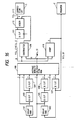
- Fig. 5 is a block diagram showing the details of the binarizing circuit D in Fig. 4.
- In Fig. 5,
reference numerals ROM 8 with the multi-level data of the target pixel; 11 the D F/F; 12 an ROM for calculating difference data to be added to the multi-level data which is input subsequently to the target pixel; and 13 an adder for adding the input data and the difference data which is output from theROM 12. - In the above construction, the
comparator 10 outputs data B(i,j) of one-bit which was binarized on the basis of theequation ③ to the D F/F 7 and the printer E. The binary data is input to theRAMs RAM 2 and the binary data B(i-2,j + 1) which was delayed by two lines by theRAM 1 are output to theROM 8. - Further, the D F/
F 3 outputs the binary data B(i-2,j) to theROM 8; the D F/F 4 outputs the B(i-2, j-1); the D F/F 5 outputs the B(i-1,j); D F/F 6 outputs the B(i-1,j-1); and the D F/F 7 outputs the B(i,j-1), respectively, to theROM 8. - As shown in Fig. 1, the binary data relates to binary images of the peripheral pixel for the input image f-(i,j). If the binary images are connected to input addresses in the
ROM 8, the binary threshold value can be obtained at a high speed because the binary threshold value (mi(i,j) + mo(i,j))/2 shown in theequation ③ has previously been stored in theROM 8 on the basis of theequations - The binary threshold value is input to the
subtracter 9 andcomparator 10. On the other hand, f(i,j) + E-(i,j) is input from the D F/F 11 to thesubtracter 9 andcomparator 10. - On the basis of those two inputs, the
subtracter 9 calculates the difference
f(i,j) + E(i,j) - (m1(i,j) + mo(i,j))/2
between both sides of the inequality in theequaiton ③. The difference value is input to theROM 12. When the above equation is modified by using theequations ① to ③, we have
- On the other hand, on the basis of the above two inputs, the
comparator 10 compares f(i,j) + E(i,j) and (m1(i,j) + mo(i,j))/2 and outputs the binary data B(i,j). - That is, in the
ROM 12, the E(i,j + 1) shown in theequation ④ is calculated on the basis of the value of B(i,j) from thecomparator 10 and f(i,j) + E(i,j) - (mi(i,j) + ma(i,j))/2 from thesubtracter 9. - In the
above equation ④, since the weight R(0,0) and S have already been known, by previously calculating the difference E(i,j + 1) from the average density value and storing into thedifference calculation ROM 12, if the binary data B(i,j) and
f(i,j) + E(i,j) - (m1(i,j) + m0(i,j))/2
as the output of thesubtracter 9 are input to theROM 12, E(i,j + 1) can be obtained by the table conversion. - Fig. 6 shows an example of the table stored in the
ROM 12. - In the embodiment, since the
weight mask 1 shown in Fig. 3 has been used, in order to normalize to the 6-bit image density levels (0 to 63) which are actually input, the values obtained by theequations weight mask 1 is set as shown in Fig. 7. - The output

subtracter 9 is input as an absolute value into theROM 12 and the positive/negative sign is determined in accordance with the value of B(i,j). The difference E(i,j + 1) obtained by theROM 12 is added to the input image data f(i,j + 1) by theadder 13. The D F/F 11 delays the addition value by a period of time of the data of one clock. - As mentioned above, the embodiment can be easily realized by merely adding calculation ICs of a few chips as compared with the average density approximating method. Moreover, the gradations can be extremely improved.
- As mentioned above, according to the above first embodiment, the average density is calculated on the basis of the binary data and the binarization is executed on the basis of the average density. Thus, a processing amount for binarization can be fairly reduced. In addition, the gradations can be remarkably improved by correcting the difference between the average density which is generated upon binarization and the input multi-level data.
- In the embodiment, the binary difference E has been distributed to only the next pixel and corrected in the equation @. However, if the binary difference E is distributed to a plurality of pixels in a manner such that 3E(i,j + 1 )/4 is distributed to the pixel (i,j + 1 ) and E(i,j + 1 )/4 is distributed to the pixel (i,j + 2) in Fig. 1, even if the average processing mask is small, the gradation reproducing capability is improved.
- The binary difference E can be also two-dimensionally distributed to a plurality of pixels near the target pixel at a predetermined distribution ratio. In this case, although a hardware construction is slightly complicated, the uniform image can be also obtained with respect to the sub scanning direction as well as in the main scanning direction and the reproducibility is improved.
- In the case of two-dimensionally distributing the binary difference E in two directions (one adjacent pixel and one pixel existing under the target pixel by one line), the
equation 0 is as follows.
- The difference transfer pixels are set to two pixel positions which are neighboring to the target pixel in two orthogonal directions, that is, two points of (i,j + 1) and (i + i,j). The difference value [f(i,j) + E(i,j) - m (i,j)] which is obtained in the embodiment is divided into two values of E1 (i,j + 1) and Edi + 1,j) and they are respectively added to the input density value, thereby executing the correction.
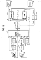
- Fig. 8 is a block diagram of a binarizing circuit in the case of two-dimensionally distributing the binary difference E. In Fig. 8, the same parts and elements as those in Fig. 5 are designated by the same reference numerals and their descriptions are omitted.
-
Reference numeral 14 denotes a distributor for distributing the binary difference E which was sent from theROM 12 into the half portions in order to distribute them to the f(i,j + 1) pixel and f(i + 1,j) pixel. -
Reference numeral 15 indicates an adder for adding f(i + 1,j) sent from the correction circuit C and E2-(i + 1,j) sent from thedistributor 14. -
Reference numeral 16 represents an RAM for delaying the data sent from theadder 15 by a period of time corresponding to one line - one pixel. By providing theRAM 16, the difference generated at the previous line can be added to the target pixel f(i,j). - As mentioned above, by two-dimensionally distributing the difference between the average density which is generated upon binarization and the input density, the regularity can be lightened as compared with the case of distributing the difference to one adjacent pixel and the generation of a periodic pattern can be prevented. On the other hand, even when an edge portion of a character, a diagram, or the like is reproduced, the directivity does not appear and the edge portion can be clearly reproduced.
- In the above embodiment, the
weighting mask 1 shown in Fig. 3 has been used as a weighting mask to obtain the average density. However, by enlarging a region to obtain the average density like aweighting mask 2, the reproducibility of the gradations can be also further improved and the reproducibility of the resolution information which is required in a character original or the like is also improved. The weighting mask is not limited to the above masks, but any mask of a similar form can be also used. - On the other hand, although the weighting mask has been set to increase as the pixel to be processed is near the target pixel, its gradient and distribution are not limited. Pixels at discrete positions which are not neighboring can be also used.
- In the embodiment, when the difference which is distributed to peripheral pixels is obtained by the error diffusion method, the inevitably dividing process is unnecessary. The difference generated in such a case is eliminated and the densities of the input image and output image can be completely preserved.
- In the
embodiment 1, the value which was corrected by adding the difference E(i,j) generated when the previous pixel (i,j-1) of the target pixel (i,j) is binarized to f(i,j) of the target pixel is compared with the. average density, thereby executing the binarization. However, in the embodiment, the difference E(i,j) is corrected upon calculation of the average value when the target pixel is binarized, thereby executing the binarization. - That is, in the
embodiment 2, mi (i,j) and mo(i,j) obtained by theequations embodiment 1 are set as follows.

- The multi-level density f(i,j) of the target pixel is binarized by the following equations.

- Fig. 9 is a block diagram of an image processing apparatus which realizes the
embodiment 2. - In Fig. 9,
reference numerals 1 to 12 indicate the same component elements as those in theembodiment 1 and their descriptions are omitted.Reference numeral 20 denotes a subtracter to subtract the difference E(i,j) generated at the previous pixel from the average density value sent form the averagedensity calculation ROM 8. In the above construction, the threshold value (m1(i,j) + mo'(i,j))/2 obtained by correcting the binary difference E by thesubtracter 20 for the average density which was output from theROM 8 is input to thesubtracter 9 andcomparator 10. On the other hand, the multi-level data f(i,j) of the input image is input to thesubtracter 9 andcomparator 10. - On the basis of those two inputs, the
subtracter 9 calculates the difference
f(i,j) - (m1(i,j) + m0(i,j))/2
between both sides of the inequality in theequation ⑦. When the above equation is modified by using theequations 

- On the other hand, the
comparator 10 compares f(i,j) with (m1(i,j) + mo (i,j))/2 and outputs the binary data B(i,j). - In the above equation since the weight R(0, 0) and S have already been known, the binary difference E(i,j + 1) is derived by the
ROM 12. The difference E(i,j + 1 ) is delayed by the D F/F 11 and is input to thesubtracter 20. By repeating the above processes, the input multi-level data can be sequentially binarized. Although theembodiments - Although the embodiments have been described with respect to the case where the number of kinds of the input data is set to one (one color), by setting the input data to three colors of R, G, and B, the invention can be also applied to a color image.
- A modified example of the
embodiment 1 will now be described as anembodiment 3. - In the
embodiment 3, when the data (f(i,j) + E(i,j)) (Fig. 2) in which the difference was corrected as described in theembodiment 1 lies within a predetermined range, the difference E(i,j+1) is corrected in a manner such that E(i,j + 1 ) = f(i,j) + E(i,j) - mo (i,j)). That is, when the difference E(i,j + 1) upon binarization of the next pixel is

- That is, the characteristic processes of the present system are as follows. As shown in the
equations equation ⑩ . On the other hand, when such a difference is out of the predetermined region, that is, when the difference between the target pixel correction values mi and mo is sufficiently large, the correction value is set to 0 and the correction upon binarization of the next pixel is not executed. - In other words, in the former case, the density change of the image near the target pixel is small, so that it is determined such that the image relates to the image area having a half tone. Therefore, the difference between the image density and the average density value generated by binarizing is corrected by the next pixel, thereby enabling the gentle density change of the image to be false half-tone processed with a high fidelity. Namely, the gradations can be improved. On the other hand, in the latter case, it is determined that the edge portion of a character, a diagram, or the like, namely, the target pixel density contrarily suddenly changes as compared with the density of the image near the target pixel. Therefore the correction value is set to 0 for the pixel in such a case and the deterioration in resolution due to the preservation of the density is suppressed, thereby binarizing and reproducing. Due to this, the resolution in the edge portion can be improved.
- As mentioned above, according to the characteristic processing system of the third embodiment, in the half-tone image region, the density is preserved on the binary image by using the binary difference in accordance with the image density change and in a resolution image portion of a character or the like, in order to prevent the fading of the image due to the preservation of the density, the binary difference is not corrected but is approximated to the average density values m1 and mo.
- Since the schematic circuit construction of the
embodiment 3 is similar to that shown in Fig. 4, its description is omitted. - Fig. 10 is a block diagram showing the details of the binarizing circuit D in the
embodiment 3. - In the diagram, the same parts and components as those in Fig. 5 are designated by the same reference numerals.
- In Fig. 10,
reference numerals ROM 8 with the multi-level data of the target pixel; 11 the D F/F; 100 an ROM for calculating difference data to be added to the multi-level data which is input next to the target pixel; and 13 the adder for adding the input data and the difference data which is output from theROM 100. - In the above construction, the
comparator 10 outputs the data B(i,j) of one-bit which was binarized on the basis of theequation ③ to the D F/F 7 and the printer E. The binary data is input to theRAMs RAM 2 is output to theROM 8. The binary data B(i-2, j + 1) which was delayed by two lines by theRAM 1 is output to theROM 8. - Further, the D F/
F 3 outputs the B(i-2,j), the D F/F 4 outputs the B(i-2,j-1), the D F/F 5 outputs the B(i-1,j), the D F/F 6 outputs the B(i-1 ,j-1), and the D F/F 7 outputs the B(i,j-1), respectively, to theROM 8. - For the input image f(i,j), the binary data relates to the binary images of the peripheral pixels as shown in Fig. 1. If the binary images are connected to input addresses in the
ROM 8, the binary threshold value can be obtained at a high speed because the binary threshold value (mi(i,j) + mo(i,j))/2 shown in theequation ③ has previously been stored in theROM 8 on the basis of theequations - The threshold value is input to the
subtracter 9 andcomparator 10. On the other hand, f(i,j) + E(i,j) is input from the D F/F 11 to thesubtracter 9 andcomparator 10. - On the basis of-those two inputs, the
subtracter 9 calculates the difference f(i,j) + E(i,j) - (mi(i,j) + mo(i,j))/2 between both sides of the inequality in theequation ③. When the above equation is modified by using theequations 

- On the other hand, on the basis of the above two inputs, the
comparator 10 compares f(i,j) + E(i,j) and (m1(i,j) + mo(i,j))/2 and outputs the binary data B(i,j). - That is, in the
ROM 100, the E(i,j+1) shown in theequation comparator 10 and f(i,j) + E(i,j) - (m1(i,j) + Mα(i,j))/2 from thesubtracter 0. - In the
equation ⑪ , since the weight R(0,0) and S have already been known, the binary difference E-(i,j + 1) according to theequations difference calculation ROM 100. Due to this, the E(i,j+1) is obtained by the table conversion by inputting the binary data B(i,j) and
f(i,j) + E(i,j) - (m1 (i,j) + mo(i,j))/2
as an output of thesubtracter 9 into theROM 12. - Fig. 11 shows an example of the table stored in the
ROM 100. - In the embodiment, the
weight mask 1 shown in Fig. 3 has been used. Therefore, in order to normalize to the image density levels (0 to 63) of six bits which are actually input, the value obtained by theequations weight mask 1 is set as shown in Fig. 7. - Fig. 11 shows the table in the case where a = 1 in the equation @. When E(i,j + 1) is larger than R(0,0) = 18, E(i,j + 1) is set to 0.
- The output f(i,j) + E(i,j) - (mi(i,j) + mo(i,j))/2 of the
subtracter 9 is input as an absolute value into theROM 100. The positive/negative sign is determined in accordance with the value of B(i,j). - The difference E(i,j + 1) obtained in the
ROM 100 is added to the input image data f(i,j + 1) by theadder 13. The D F/F 11 delays the addition value by a period of time of one clock of the data. - As mentioned above, as compared with the average density approximating method, the
embodiment 3 can be easily realized by merely adding calculation ICs of a few chips. - As described above, according to the
embodiment 3 of the invention, the average density is calculated on the basis of the data which has already been binarized and the binarization is executed on the basis of the average density, so that a processing amount for binarization can be remarkably reduced. Moreover, when the difference between the average density which is generated upon binarization and the input multi-level data lies within a predetermined range, the difference is corrected, so that the half-tone process having the excellent gradations can be executed. - Further, in the embodiment, when the difference between the average density and the input multi-level data is larger than the predetermined value, the difference is not corrected. Thus the deterioration in resolution due to the preservation of the densities is prevented and the edge portion can be clearly reproduced.
- In the embodiment, the binary difference E has been distributed to only the next pixel and the correction has been executed in the equation @. However, the binary difference E can be also two-dimensionally distributed to a plurality of pixels near the target pixel at a predetermined distribution ratio. In this case, although a hardware construction is slightly complicated, the uniform image can be also obtained with respect to the sub scanning direction as well as the main scanning direction and the reproducibility is improved.
- On the other hand, for instance, in Fig. 1, if the binary difference E is distributed to a plurality of pixels in a manner such that 3E(i,j + 1 )/4 is distributed to the pixel (i,j + 1) and E(i,j + 1 )/4 is distributed to the pixel (i,j+2), the reproducing capability of the gradations is improved even if the average processing mask is small.
- On the other hand, although the weighting mask is increased as the pixel is near the target pixel, its gradient and distribution are not limited. The pixels existing at discrete positions which are not neighboring can be also used.
- On the other hand, the invention can be widely used in image processing apparatuses such as facsimile apparatus, copying machine, and the like.
- In the
embodiment 3, the binary difference E has been divided to the cases shown by theequations - For instance, as shown in Fig. 12, if the value of α is set so as to decrease as the average density approaches 0 or 1, the edge portion of a black character in the white background, a blank character in the black background, or the like can be more finely binarized.
- The following
equation ⑫ is used in place of theequation ⑨ in theembodiment 3. In the case where
- Where, K is a constant and if it is set to about 0 or 1 (K = 0, 1), the good result can be obtained.
- According to the
embodiment 5, by setting the difference E to 0 in the case where the average density value approached 0 or 1, the character portion can be highly finely binarized in a manner similar to theembodiment 2. - In the
embodiments density calculation ROM 8 is input in place of the binary data B(i,j) to an address terminal of thedifference calculation ROM 100, those embodiments can be easily realized by the table converting processes based on the data which has previously been written in a manner similar to theembodiment 3. - In the
embodiment 3, the weighting mask of the matrix of 3 x 3 shown in Fig. 3 has been used. However, generally, in order to smoothly binarize the half-tone portion, it is desirable to set the weight R-(0,0) of the target pixel to a small value. In addition, as the weight R(0,0) is small for a density change of the data to be binarized, the edge portion shown by the equation @ can be accurately detected. Therefore, in the case of using the weighting mask of 4 x 5 shown in Fig. 14, R(0,0) in Fig. 3 in theembodiment 3 is set to 8/28 = 0.29, while that in Fig. 13 is set to 11/96 = 0.11. Thus, the half-tone portion can be more smoothly binarized and the edge portion of a character portion or the like can be more finely binarized and reproduced. - In the
embodiments 3 to 6, the calculation of the correction value E for preservation of all densities during the processing has been executed by using the average values mo and m1. However, for instance, the discrimination or the like to see if the value of E is set to 0 or not in the edge portion or the like can be realized by a well-known technique. For example, a two-dimensional Laplacian is obtained from the image data to be binarized, this value is processed on the basis of the threshold value, the edge portion is determined on the basis of the result of the discrimination of such a threshold value processing, and E is set to 0 in the edge portion. Even by this method, the similar effect is derived. On the other hand, the edge portion is designated in a wide region on the basis of a command obtained by an area designating operation of the operator without switching the processes every pixel and E can be also set to 0 in such a region. - In the
above embodiments 1 to 6, assuming that the average value when the target pixel was binarized to 0 is set to mi and the average value when the target pixel was binarized to 1 is set to mo, the data of the target pixel is binarized by using (mi + mo)/2 as a threshold value. - In the embodiment which will be explained hereinlater, explanation will now be made with respect to an example in the case where the average value of the binary data (the data which has previously been binarized before the target pixel) including no target pixel is set to a threshold value and the data of the target pixel is binarized.
- The principle of the above system will be first described.
- Fig. 14(1) is a diagram showing a multi-level density of each pixel of the input image.
- In Fig. 14(1), f(i,j) denotes multi-level density data of the input image at the position of the target pixel to be binarized and is set to a normalized value of 0 to 1. On the other hand, the binarization has already been finished at the pixel positions above a broken line. After the target pixel was binarized, the similar binarization is sequentially executed in a manner such that f(i,j + 1), f(i,j + 2), ....
- Fig. 14(2) is a diagram showing binary image data. B(i,j) shows the density (having the value of 0 or 1) after the target pixel was binarized. The portion surrounded by a broken line denote the pixel data which has already been binarized upon processing of the target pixel. Those pixel data are used to binarize the target pixel.
- Fig. 14(3) is a diagram showing weighting masks. R denotes an example of the weighting mask to obtain the average density and is expressed by a matrix of a size of 3 x 3. The weight R(0,0) for the pixels which are not binarized yet is used by setting such that R(0,0) = R(0,-1) = 0.
- In the system, the weighted average density of the binary images near the target pixel is set to m(i,j) and is obtained by the following equation.

- The target pixel f(i,j) is binarized by using the average density m(i,j) and the binary correction value E-(i,j) which has already been assigned in accordance with the following equation.

- Fig. 15 is a diagram showing the
equation ⑭ . - In the equation ⑭ E(i,j) denotes a difference which is generated when the multi-level density f(i,j-1) of the pixel which is precedent to the target pixel (i,j) by one pixel, that is, of the pixel (i,j-1) was binarized to the binary density B(i,j-1). Namely, E(i,j) corresponds to the difference value between the multi-level density f(i,j-1) and the average density m(i,j-1) of the pixel near the target pixel. By binarizing the corrected value which is obtained by adding the binary difference E(i,j) to the target pixel f(i,j), the image density after completion of the binarization can be completely preserved as an average density in the whole input image region.
- By executing the processes in consideration of the binary difference, the reproducing capability of the half tone is remarkably improved as compared with that in the average density approximating method.
- On the other hand, in the equation @ , E(i,j + 1) denotes a difference which is distributed to the pixel f(i,j + 1) which is located behind the target pixel (i,j) by one pixel.
- The reason why in spite of the fact that a processing amount in the binarization system in the embodiment is extremely smaller than that in the error diffusion method, the image reproducing capability which is equal to or higher than that in the error diffusion method is obtained is because in spite of the fact that the difference is merely corrected by one adjacent pixel, by obtaining the average density by using a plurality of data after completion of the binarization, the effect similar to that in the case of distributing the difference to a plurality of pixels and correcting is equivalently obtained.
- Since a schematic circuit construction in the embodiment is similar to that shown in Fig. 4, its description is omitted.
- Fig. 16 is a block diagram showing the details of the binarizing circuit D in the
embodiment 7. - In Fig. 16,
reference numerals ROM 108; 110 a comparator for comparing the threshold value which is output from theROM 108 with the multi-level data of the target pixel; and 112 an adder for adding the difference data which is output from thesubtracter 109 and the 6-bit multi-level data sent from the correction circuit. - In the above construction, the
comparator 110 outputs the 1-bit data B(i,j) which was binarized on the basis of the equation @ . The binary data is input to theRAMs RAM 102 is output to theROM 108. The binary data B(i-2,j + 1) which was delayed by two lines by theRAM 101 is output to theROM 108. - Further, the D F/
F 103 outputs the B(i-2,j), the D F/F 104 outputs the B(i-2,j-1), the D F/F 105 outputs the B(i-1,j), the D F/F 106 outputs the B(i-1,j-1), and the D F/F 107 outputs the B(i,j-1), respectively, to theROM 108. - The binary data denote the binary images of the peripheral pixels for the input image f(i,j) as shown in Fig. 14. By connecting the binary images to input addresses in the
ROM 108, the binarization threshold value can be obtained at a high speed because the binarization threshold value m(i,j) shown in the equation @ has previously been stored in theROM 108 on the basis of the equation @ - The threshold value is input to the
subtracter 109 andcomparator 110. On the other hand, f(i,j) + E(i,j) is input from the D F/F 111 to thesubtracter 109 andcomparator 110. - On the basis of those two inputs, the
subtracter 109 calculates the difference
- On the other hand, the
comparator 110 compares f(i,j) + E(i,j) and m(i,j) on the basis of the two inputs and outputs the binary data B(i,j). On the other hand, on the basis of the equation @ , the difference E-(i.j+1) which is output from thesubtracter 109 is added to the input image data f(i,j+1) by theadder 112. The D F/F 111 delays the addition value by a period of time of one clock of the data. - Fig. 17 shows examples of the weighting masks. The weighting mask of Fig. 17A is used to obtain the average value from the binary data of seven pixels. The weighting mask of Fig. 17B is used to obtain the average value from the binary data of twelve pixels. In the embodiment, since the weighting mask shown in Fig. 17A is used, in order to normalize to the image density levels (0 to 63) of six bits which are actually input, the values obtained by the equation @ are increased by 63 times and the resultant values are stored into the average density calculation ROM table as the values which were converted into the 6-bit values.
- As described above, according to the
embodiment 7, the average density is calcualted by using only the binary data which was binarized and the input multi-level data is binarized by using the average density as a threshold value. Therefore, a processing amount for binarization can be reduced as compared with that in the average density approximating method. Moreover, since the difference between the input multi-level data and the average density which is generated when the input multi-level data was binarized is corrected the gradations can be extremely improved. - In the embodiment, although the binary difference E has been distributed to only the next pixel and corrected, if the binary difference E is distributed to a plurality of pixels in the main scanning direction in a manner such that, for instance, in Fig. 14, 3E(i,j + 1 )/4 is distributed to the pixel (i,j + 1) and E(i,j + 1 )/4 is distributed to the pixel (i,j+2), the reproducing capability of the gradations is improved even when the average processing mask is small.
- On the other hand, the binary difference E can be also two-dimensionally distributed to a plurality of pixels near the target pixel at a predetermined distribution ratio in a manner similar to the case of the error diffusion method. In this case, although a hardware construction is slightly complicated, the uniform image can be obtained in the sub scanning direction as well as the main scanning direction and the reproducibility is improved.
- On the other hand, although the weighting mask has been increased as the pixel is close to the target pixel, its gradient and distribution are not limited. The pixels at the discrete positions which are not neighboring can be also used.
- In the
embodiment 7, the weighting mask of a matrix of 3 x 3 such as shown in an example of Fig. 17A has been used. However, generally, in order to smoothly binarize the half-tone portion, it is desirable to set the weight of the pixel adjacent to the target pixel to a small value. - Therefore, in the case of using the weighting matrix of a matrix of 3 x 5 shown in Fig. 17B, R(i-1,j) and R(i,j-1) are set to 7/48 = 0.15 as compared with 5/21 = 0.24 in the matrix of Fig. 17A, so that the half-tone portion can be smoothly binarized and reproduced.
- In the embodiment, the calculation of the average density m has easily been realized by the ROM table. However, such a calculation can be also realized even by using seven AND gates and a plurality of adders. In this case, the processing speed can be further made high. On the other hand, by assembling such a processing circuit into a gate array or the like, a hardware scale can be remarkably reduced.
- In the embodiment, the correction has been performed by directly adding the binary difference E(i,j) to the target pixel density f(i,j). However, as shown in Fig. 18, even when the difference E(i,j) is corrected by subtracting it from the average density by using a
subtracter 113, the similar effect can be also obtained. - The
embodiment 8 relates to a partially modified form of theembodiment 7. - That is, in the
embodiment 8, the difference E(i,j + 1) when the next pixel is binarized is expressed by the following equation. In the case where

- Therefore, as shown in the equations @ and in the comparison between the average density m upon binarization and the corrected target pixel density in which the difference was corrected, if the corrected target pixel density lies within a predetermined range of a value near the average density m (that is, when the difference between the average density m and the corrected target pixel density lies within a predetermined range), the difference between the corrected target pixel density and the average density is assigned as a correction value when the next pixel is binarized in accordance with the equation @ . On the other hand, if it is out of the predetermined range, that is, when the difference between the corrected target pixel density and the average density is sufficiently large, the correction value is set to 0 and the correction upon binarization of the next pixel is not executed. Namely, in the case of correcting the difference, the density change of the image near the target pixel is small, so that it is determined that such as image is in the image area having a half-tone. Therefore, the difference between the image density and the average density which occurs due to the binarization is corrected by the next pixel, so that the gentle density change of the image can be false half-tone processed with a high fidelity. That is, the gradations can be improved. On the other hand, in the case where the difference is not corrected, the edge portion in a character, a diagram, or the like, that is, the target pixel is contrarily determined to be suddenly changed as compared with the density of the image near the target pixel. Thus, the correction value is set to 0 for the pixel in such a case and the deterioration in resolution due to the preservation of the density is suppressed, thereby binarizing and reproducing. Consequently, the resolution in the edge portion can be improved.
- As mentioned above, according to the characteristic processing system of the
embodiment 8, in the half-tone image area, the density is preserved on the binary image by using the binary difference in accordance with the image density change. In the resolution image portion such as a character or the like, in order to prevent the fading of the image due to the preservation of the density, the correction of the binary difference is not executed by the density is approximated to the average density m. - Since a schematic circuit construction in the
embodiment 8 is similar to that shown in Fig. 4, its description is omitted. - Fig. 19 is a block diagram showing the details of the binarizing circuit D in the
embodiment 8. - In Fig. 19, the same parts and elements as those shown in Fig. 16 are designated by the same reference numerals and their descriptions are omitted.
-
Reference numeral 115 denotes a comparator for comparing the difference between the multi-level data of the target pixel which is sent from thesubtracter 109 and the threshold value with a predetermined value ( α ).Reference numeral 116 indicates a selector for selecting either 0 or an output of thesubtracter 109 on the basis of a select signal from the comparator. - In Fig. 19, the
comparator 110 outputs the 1-bit data B(i,j) which was binarized on the basis of the equation @ . The binary data is input to theRAMs RAM 102 is output to theROM 108. The binary data B(i-2,j+1) which was delayed by two lines by theRAM 101 is output to theROM 108. - Further, the D F/
F 103 outputs the B(i-2,j), the D F/F 104 outputs the B(i-2,j-1), the D F/F 105 outputs the B(i-1,j), the D F/F 106 outputs the B(i-1, j-1), and the D F/F 107 outputs the B(i,j-1), respectively, to theROM 108. - As shown in Fig. 14, the binary data denotes the binary images of the peripheral pixels for the input image f(i,j). By connecting the binary images to input addresses in the
ROM 108, the binarization threshold value can be obtained at a high speed because the binarization threshold value m(i,j) shown in the equation @ has previously been stored in theROM 108 on the basis of the equation @ . - The threshold value is input to the
subtracter 109 andcomparator 110. On the other hand, f(i,j) + E(i,j) is input from the D F/F 111 to thesubtracter 109 andcomparator 110. - On the basis of the two inouts, the
subtracter 109 calculates the difference
equation ⑭ . - On the other hand, the
comparator 110 compares f(i,j) + E(i,j) with m(i,j) on the basis of the two inputs and outputs the binary data B(i,j). On the other hand, the difference E(i,j + 1) which is output from thesubtracter 109 is input to theselector 116 and thecomparator 115 on the basis of theequation ⑱ - The
comparator 115 compares the difference E(i,j + 1) with the constant a by theequation ⑯ and outputs the select signal to theselector 116 on the basis of the result of the comparison. - As a result of the select signal sent from the
comparator 115, when the absolute value of the difference E(i,j+1) is larger than α theselector 116 selects and outputs-E(i,j + 1) = 0. If it is equal to or less than α, theselector 116 directly selects and outputs the output signal of thesubtracter 109. - The difference E(i,j+1) is added to the input image data f(i,j+1) by the
adder 112. The D F/F 111 delays the addition value by a period of time of one clock of the data. - In a manner similar to the above, by repeating the above processes, the binarization is sequentially executed.
- The weighting mask shown in Fig. 17 is used.
- As described above, according to the
embodiment 8, the average density is calculated by using only the binary data which was binarized and the input multi-level data is binarized by using the average density as a threshold value. Therefore, a processing amount for binarization can be reduced as compared with that in the average density approximating method. Moreover, when the difference between the input multi-level data which is generated upon binarization of the input multi-level data and the average density lies within a predetermined range, the difference is corrected, so that the gradations can be remarkably improved. - Further, in the embodiment, when the difference between the average density and the input multi-level data is larger than a predetermined value, the difference is not corrected. Thus, the deterioration in resolution due to the preservation of the density is prevented and the edge portion can be clearly reproduced.
- In the embodiment, the binary difference E has been distributed to only the next pixel and corrected. However, if the binary difference E is distributed to a pluraltiy of pixels in the main scanning direction in a manner such that, for instance, in Fig. 14, 3E(i,j+ 1 )/4 is distributed to the pixel (i,j + 1) and E(i,j + 1 )/4 is distributed to the pixel (i,j+2), the reproducing capability of the gradations is improved even if the average processing mask is small.
- On the other hand, the binary difference can be also two-dimensionally distributed to a plurality of pixels near the target pixel at a predetermined distribution ratio in a manner similar to the case of the error diffusion method. In this case, although a hardware construction is slightly complicated, the uniform image can be obtained in the sub scanning direction as well as the main scanning direction and the reproducibility is improved.
- On the other hand, although the weighting mask has been increased as the pixel is close to the target pixel, its gradient and distribution are not limited. The pixels existing at the discrete positions which are not neighboring can be also used.
- In the
embodiment 8, the binary difference E has been divided into two cases shown by the equations @ and @ and when the difference E is equal to or larger than a predetermined value using the constant α , the difference E is set to 0 and is not distributed to the next pixel. However, the value of the constant a can be also changed in accordance with the average density value or target pixel density value. - For instance, as shown in Fig. 20, if the value of a is set to be reduced as the average density approaches 0 or 1, the edge portion of a black character in the white background, a blank character in the black background, or the like can be more finely binarized.
- The following equation @ can be also used in place of the equation @ in the
embodiment 8.
- According to the embodiment, by setting the difference E to 0 in the case where the average density value approached 0 or 1, the character portion can be finely binarized in a manner similar to the
embodiment 9. - As shown in Fig. 21, in the
embodiments density calculation ROM 108 to an address terminal in adifference calculation ROM 120, those embodiments can be easily realized by the table converting processes based on the data which has previously been written. - In the
embodiment 8, the weighting mask of a matrix of 3 x 3 as shown in an example of Fig. 17A has been used. However, generally, to smoothly binarize the half-tone portion, it is desirable to set the weight of the pixel adjacent to the target pixel to a small value. - Therefore, in the case of using the weighting mask of a matrix of 3 x 5 shown in Fig. 17B, R(i-1,j) and R(i,j-1) in Fig. 17B are set to 7/48 = 0.15 while those in Fig. 17A in the
embodiment 8 are set to 5/21 = 0.24, so that the half-tone portion can be more smoothly binarized and reproduced. - In the
embodiment 8, the calculation of the average density m has easily been realized by the ROM table. However, such calculation can be also realized by using seven AND gates and a plurality of adders. In this case, the processing speed can be further made high. On the other hand, by assembling such a processing circuit into a gate array or the like, a hardware scale can be remarkably reduced. - In the embodiment, the average density m which is used in the present system has been used in the calculation of the correction value E for preservation of all densities during the processing. However, the determination or the like to see if E is set to 0 or not in the edge portion or the like can be also realized by the well-known technique. For instance, a two-dimensional Laplacian is obtained from the image data to be binarized, this value is processed to a threshold value, the edge portion is discriminated on the basis of the result of the discrimination of such a threshold value process, and E is set to 0 in the edge portion. The similar result is also obtained even by such a method. On the other hand, the edge portion is designated in a wide area on the basis of a command obtained by the area designating operation by the operator without switching the process every pixel and E can be also set to 0 in such an area.
- On the other hand, although the embodiment has been described with respect to the case where the number of kind of the input data is one (one color), the invention can be also applied to a color image by setting the input data to three colors of R, G, and B.
- As described above, according to the invention, an image having excellent gradation and resolution can be obtained in a short time by a simple hardware construction.
- The present invention is not limited to the foregoing embodiments but many modifications and variations are possible within the spirit and scope of the appended claims of the invention.
- Attention is drawn to concurrently filed related application (EP-A- ), agents' reference 2120530, which is incorporated herein by reference and a copy of which is filed herewith.
Claims (20)
Applications Claiming Priority (12)
| Application Number | Priority Date | Filing Date | Title |
|---|---|---|---|
| JP1031408A JP2810395B2 (en) | 1989-02-10 | 1989-02-10 | Image processing device |
| JP31405/89 | 1989-02-10 | ||
| JP1031409A JP2683085B2 (en) | 1989-02-10 | 1989-02-10 | Image processing device |
| JP31404/89 | 1989-02-10 | ||
| JP1031404A JPH02210959A (en) | 1989-02-10 | 1989-02-10 | Picture processor |
| JP31409/89 | 1989-02-10 | ||
| JP1031411A JP2810396B2 (en) | 1989-02-10 | 1989-02-10 | Image processing device |
| JP31411/89 | 1989-02-10 | ||
| JP1031405A JP2683084B2 (en) | 1989-02-10 | 1989-02-10 | Image processing device |
| JP31408/89 | 1989-02-10 | ||
| JP1284879A JPH03147480A (en) | 1989-11-02 | 1989-11-02 | Picture processing unit |
| JP284879/89 | 1989-11-02 |
Publications (3)
| Publication Number | Publication Date |
|---|---|
| EP0382581A2 true EP0382581A2 (en) | 1990-08-16 |
| EP0382581A3 EP0382581A3 (en) | 1991-10-16 |
| EP0382581B1 EP0382581B1 (en) | 1996-05-08 |
Family
ID=27549596
Family Applications (2)
| Application Number | Title | Priority Date | Filing Date |
|---|---|---|---|
| EP19900301475 Expired - Lifetime EP0382580B1 (en) | 1989-02-10 | 1990-02-12 | Image processing apparatus |
| EP19900301476 Expired - Lifetime EP0382581B1 (en) | 1989-02-10 | 1990-02-12 | Image processing apparatus |
Family Applications Before (1)
| Application Number | Title | Priority Date | Filing Date |
|---|---|---|---|
| EP19900301475 Expired - Lifetime EP0382580B1 (en) | 1989-02-10 | 1990-02-12 | Image processing apparatus |
Country Status (2)
| Country | Link |
|---|---|
| EP (2) | EP0382580B1 (en) |
| DE (2) | DE69027870T2 (en) |
Cited By (4)
| Publication number | Priority date | Publication date | Assignee | Title |
|---|---|---|---|---|
| EP0395404A3 (en) * | 1989-04-27 | 1992-06-03 | Canon Kabushiki Kaisha | Image processing apparatus |
| EP0712235A2 (en) * | 1994-11-08 | 1996-05-15 | Xerox Corporation | Pixel pair grid halftoning for a hyperacuity printer |
| EP0893910A1 (en) * | 1997-07-21 | 1999-01-27 | SYFAL S.p.A. | A process for reproducing high-definition images |
| US6118485A (en) * | 1994-05-18 | 2000-09-12 | Sharp Kabushiki Kaisha | Card type camera with image processing function |
Families Citing this family (4)
| Publication number | Priority date | Publication date | Assignee | Title |
|---|---|---|---|---|
| US5515180A (en) * | 1992-11-24 | 1996-05-07 | Sharp Kabushiki Kaisha | Image processing device |
| EP0670654B1 (en) * | 1994-03-02 | 2001-04-18 | Hewlett-Packard Company, A Delaware Corporation | Multiple tone image generation |
| EP0670653B1 (en) * | 1994-03-02 | 2001-07-11 | Hewlett-Packard Company, A Delaware Corporation | Multiple tone image generation |
| US7268919B2 (en) | 2002-01-17 | 2007-09-11 | Seiko Epson Corporation | Image data processing apparatus, method, and program that diffuses gradiation error for each pixel in target block |
Citations (3)
| Publication number | Priority date | Publication date | Assignee | Title |
|---|---|---|---|---|
| JPS57104369A (en) * | 1980-12-22 | 1982-06-29 | Toshiba Corp | Binary device for picture with contrast |
| US4622595A (en) * | 1983-12-21 | 1986-11-11 | Fuji Xerox Co., Ltd. | Image display unit capable of tone reproduction |
| EP0279419A2 (en) * | 1987-02-17 | 1988-08-24 | Sharp Kabushiki Kaisha | Image signal binary encoder |
Family Cites Families (3)
| Publication number | Priority date | Publication date | Assignee | Title |
|---|---|---|---|---|
| JPS60214160A (en) * | 1984-04-09 | 1985-10-26 | Ricoh Co Ltd | Picture signal binary-coding system |
| US4692811A (en) * | 1984-07-25 | 1987-09-08 | Matsushita Electric Industrial Co., Ltd. | Apparatus for processing image signal |
| EP0248616A3 (en) * | 1986-06-02 | 1990-03-07 | Kabushiki Kaisha Toshiba | Picture printing apparatus |
-
1990
- 1990-02-12 DE DE1990627870 patent/DE69027870T2/en not_active Expired - Fee Related
- 1990-02-12 DE DE1990626846 patent/DE69026846T2/en not_active Expired - Fee Related
- 1990-02-12 EP EP19900301475 patent/EP0382580B1/en not_active Expired - Lifetime
- 1990-02-12 EP EP19900301476 patent/EP0382581B1/en not_active Expired - Lifetime
Patent Citations (3)
| Publication number | Priority date | Publication date | Assignee | Title |
|---|---|---|---|---|
| JPS57104369A (en) * | 1980-12-22 | 1982-06-29 | Toshiba Corp | Binary device for picture with contrast |
| US4622595A (en) * | 1983-12-21 | 1986-11-11 | Fuji Xerox Co., Ltd. | Image display unit capable of tone reproduction |
| EP0279419A2 (en) * | 1987-02-17 | 1988-08-24 | Sharp Kabushiki Kaisha | Image signal binary encoder |
Non-Patent Citations (2)
| Title |
|---|
| LINKS FOR THE FUTURE, IEEE INTERNATIONAL CONFERENCE ON COMMUNICATIONS, Amsterdam, 14th - 17th May 1984, The Netherlands Proceedings, vol. 1, pages 228-233; K. NAKAZATO et al.: "Halftoning of continuous-tone image reproduction with alias suppression" * |
| PATENT ABSTRACTS OF JAPAN, vol. 6, no. 194 (E-134), 2nd October 1982; & JP-A-57 104 369 (TOSHIBA CORP.) 29-06-1982 * |
Cited By (5)
| Publication number | Priority date | Publication date | Assignee | Title |
|---|---|---|---|---|
| EP0395404A3 (en) * | 1989-04-27 | 1992-06-03 | Canon Kabushiki Kaisha | Image processing apparatus |
| US6118485A (en) * | 1994-05-18 | 2000-09-12 | Sharp Kabushiki Kaisha | Card type camera with image processing function |
| EP0712235A2 (en) * | 1994-11-08 | 1996-05-15 | Xerox Corporation | Pixel pair grid halftoning for a hyperacuity printer |
| EP0712235A3 (en) * | 1994-11-08 | 1997-12-17 | Xerox Corporation | Pixel pair grid halftoning for a hyperacuity printer |
| EP0893910A1 (en) * | 1997-07-21 | 1999-01-27 | SYFAL S.p.A. | A process for reproducing high-definition images |
Also Published As
| Publication number | Publication date |
|---|---|
| EP0382580A3 (en) | 1991-10-02 |
| DE69026846D1 (en) | 1996-06-13 |
| DE69027870T2 (en) | 1997-01-09 |
| EP0382581B1 (en) | 1996-05-08 |
| EP0382581A3 (en) | 1991-10-16 |
| EP0382580A2 (en) | 1990-08-16 |
| DE69027870D1 (en) | 1996-08-29 |
| EP0382580B1 (en) | 1996-07-24 |
| DE69026846T2 (en) | 1997-01-09 |
Similar Documents
| Publication | Publication Date | Title |
|---|---|---|
| US6118547A (en) | Image processing method and apparatus | |
| US5121447A (en) | Apparatus for performing gradation processing on image data | |
| US5008950A (en) | Image processing method and apparatus for error-dispersion digitization without moire or spurious stripe formation | |
| US5325448A (en) | Image treatment method and apparatus with error dispersion and controllable quantization | |
| US5153925A (en) | Image processing apparatus | |
| US4958238A (en) | Image processing method and apparatus with conditional correction of error data | |
| US5243445A (en) | Picture processing apparatus | |
| EP0781034B1 (en) | Image processing apparatus and method | |
| US6330075B1 (en) | Image processing method and apparatus | |
| US5208684A (en) | Half-tone image processing system | |
| US5157741A (en) | Image processing method and apparatus for out-putting dot-processed data with suppression of false contours and other noise | |
| US5577136A (en) | Image processing apparatus | |
| US6233360B1 (en) | Method and system for hybrid error diffusion processing of image information using adaptive white and black reference values | |
| EP0382581B1 (en) | Image processing apparatus | |
| US6134355A (en) | Binarization using a local average, and using error diffusion | |
| US6026199A (en) | Method and apparatus for halftoning grey value signals | |
| US5760918A (en) | Image processing apparatus with conversion and reconversion of the number of bits per pixel | |
| JP2683085B2 (en) | Image processing device | |
| JP2683084B2 (en) | Image processing device | |
| JPH01115271A (en) | Image processor | |
| US5200839A (en) | Image processing apparatus | |
| JP2810395B2 (en) | Image processing device | |
| JP2848566B2 (en) | Image processing device | |
| JP2810396B2 (en) | Image processing device | |
| JP2900907B2 (en) | Image processing device |
Legal Events
| Date | Code | Title | Description |
|---|---|---|---|
| PUAI | Public reference made under article 153(3) epc to a published international application that has entered the european phase |
Free format text: ORIGINAL CODE: 0009012 |
|
| AK | Designated contracting states |
Kind code of ref document: A2 Designated state(s): DE FR GB |
|
| 17P | Request for examination filed |
Effective date: 19901231 |
|
| PUAL | Search report despatched |
Free format text: ORIGINAL CODE: 0009013 |
|
| AK | Designated contracting states |
Kind code of ref document: A3 Designated state(s): DE FR GB |
|
| 17Q | First examination report despatched |
Effective date: 19940201 |
|
| GRAA | (expected) grant |
Free format text: ORIGINAL CODE: 0009210 |
|
| AK | Designated contracting states |
Kind code of ref document: B1 Designated state(s): DE FR GB |
|
| REF | Corresponds to: |
Ref document number: 69026846 Country of ref document: DE Date of ref document: 19960613 |
|
| ET | Fr: translation filed | ||
| PLBE | No opposition filed within time limit |
Free format text: ORIGINAL CODE: 0009261 |
|
| STAA | Information on the status of an ep patent application or granted ep patent |
Free format text: STATUS: NO OPPOSITION FILED WITHIN TIME LIMIT |
|
| 26N | No opposition filed | ||
| REG | Reference to a national code |
Ref country code: GB Ref legal event code: IF02 |
|
| PGFP | Annual fee paid to national office [announced via postgrant information from national office to epo] |
Ref country code: GB Payment date: 20080226 Year of fee payment: 19 Ref country code: DE Payment date: 20080229 Year of fee payment: 19 |
|
| PGFP | Annual fee paid to national office [announced via postgrant information from national office to epo] |
Ref country code: FR Payment date: 20080221 Year of fee payment: 19 |
|
| GBPC | Gb: european patent ceased through non-payment of renewal fee |
Effective date: 20090212 |
|
| REG | Reference to a national code |
Ref country code: FR Ref legal event code: ST Effective date: 20091030 |
|
| PG25 | Lapsed in a contracting state [announced via postgrant information from national office to epo] |
Ref country code: DE Free format text: LAPSE BECAUSE OF NON-PAYMENT OF DUE FEES Effective date: 20090901 |
|
| PG25 | Lapsed in a contracting state [announced via postgrant information from national office to epo] |
Ref country code: GB Free format text: LAPSE BECAUSE OF NON-PAYMENT OF DUE FEES Effective date: 20090212 Ref country code: FR Free format text: LAPSE BECAUSE OF NON-PAYMENT OF DUE FEES Effective date: 20090302 |