EP0384403A2 - A method for controlling a multi-gradation display and a multi-gradation display device - Google Patents
A method for controlling a multi-gradation display and a multi-gradation display device Download PDFInfo
- Publication number
- EP0384403A2 EP0384403A2 EP90103253A EP90103253A EP0384403A2 EP 0384403 A2 EP0384403 A2 EP 0384403A2 EP 90103253 A EP90103253 A EP 90103253A EP 90103253 A EP90103253 A EP 90103253A EP 0384403 A2 EP0384403 A2 EP 0384403A2
- Authority
- EP
- European Patent Office
- Prior art keywords
- dots
- effective
- gradation
- display
- image
- Prior art date
- Legal status (The legal status is an assumption and is not a legal conclusion. Google has not performed a legal analysis and makes no representation as to the accuracy of the status listed.)
- Granted
Links
Images


Classifications
-
- G—PHYSICS
- G09—EDUCATION; CRYPTOGRAPHY; DISPLAY; ADVERTISING; SEALS
- G09G—ARRANGEMENTS OR CIRCUITS FOR CONTROL OF INDICATING DEVICES USING STATIC MEANS TO PRESENT VARIABLE INFORMATION
- G09G3/00—Control arrangements or circuits, of interest only in connection with visual indicators other than cathode-ray tubes
- G09G3/20—Control arrangements or circuits, of interest only in connection with visual indicators other than cathode-ray tubes for presentation of an assembly of a number of characters, e.g. a page, by composing the assembly by combination of individual elements arranged in a matrix no fixed position being assigned to or needed to be assigned to the individual characters or partial characters
- G09G3/34—Control arrangements or circuits, of interest only in connection with visual indicators other than cathode-ray tubes for presentation of an assembly of a number of characters, e.g. a page, by composing the assembly by combination of individual elements arranged in a matrix no fixed position being assigned to or needed to be assigned to the individual characters or partial characters by control of light from an independent source
- G09G3/36—Control arrangements or circuits, of interest only in connection with visual indicators other than cathode-ray tubes for presentation of an assembly of a number of characters, e.g. a page, by composing the assembly by combination of individual elements arranged in a matrix no fixed position being assigned to or needed to be assigned to the individual characters or partial characters by control of light from an independent source using liquid crystals
- G09G3/3611—Control of matrices with row and column drivers
-
- G—PHYSICS
- G02—OPTICS
- G02F—OPTICAL DEVICES OR ARRANGEMENTS FOR THE CONTROL OF LIGHT BY MODIFICATION OF THE OPTICAL PROPERTIES OF THE MEDIA OF THE ELEMENTS INVOLVED THEREIN; NON-LINEAR OPTICS; FREQUENCY-CHANGING OF LIGHT; OPTICAL LOGIC ELEMENTS; OPTICAL ANALOGUE/DIGITAL CONVERTERS
- G02F1/00—Devices or arrangements for the control of the intensity, colour, phase, polarisation or direction of light arriving from an independent light source, e.g. switching, gating or modulating; Non-linear optics
- G02F1/01—Devices or arrangements for the control of the intensity, colour, phase, polarisation or direction of light arriving from an independent light source, e.g. switching, gating or modulating; Non-linear optics for the control of the intensity, phase, polarisation or colour
- G02F1/13—Devices or arrangements for the control of the intensity, colour, phase, polarisation or direction of light arriving from an independent light source, e.g. switching, gating or modulating; Non-linear optics for the control of the intensity, phase, polarisation or colour based on liquid crystals, e.g. single liquid crystal display cells
- G02F1/133—Constructional arrangements; Operation of liquid crystal cells; Circuit arrangements
- G02F1/1333—Constructional arrangements; Manufacturing methods
- G02F1/1343—Electrodes
- G02F1/134309—Electrodes characterised by their geometrical arrangement
- G02F1/134345—Subdivided pixels, e.g. for grey scale or redundancy
-
- G—PHYSICS
- G09—EDUCATION; CRYPTOGRAPHY; DISPLAY; ADVERTISING; SEALS
- G09G—ARRANGEMENTS OR CIRCUITS FOR CONTROL OF INDICATING DEVICES USING STATIC MEANS TO PRESENT VARIABLE INFORMATION
- G09G3/00—Control arrangements or circuits, of interest only in connection with visual indicators other than cathode-ray tubes
- G09G3/20—Control arrangements or circuits, of interest only in connection with visual indicators other than cathode-ray tubes for presentation of an assembly of a number of characters, e.g. a page, by composing the assembly by combination of individual elements arranged in a matrix no fixed position being assigned to or needed to be assigned to the individual characters or partial characters
- G09G3/2007—Display of intermediate tones
- G09G3/2018—Display of intermediate tones by time modulation using two or more time intervals
- G09G3/2022—Display of intermediate tones by time modulation using two or more time intervals using sub-frames
- G09G3/2025—Display of intermediate tones by time modulation using two or more time intervals using sub-frames the sub-frames having all the same time duration
-
- G—PHYSICS
- G09—EDUCATION; CRYPTOGRAPHY; DISPLAY; ADVERTISING; SEALS
- G09G—ARRANGEMENTS OR CIRCUITS FOR CONTROL OF INDICATING DEVICES USING STATIC MEANS TO PRESENT VARIABLE INFORMATION
- G09G3/00—Control arrangements or circuits, of interest only in connection with visual indicators other than cathode-ray tubes
- G09G3/20—Control arrangements or circuits, of interest only in connection with visual indicators other than cathode-ray tubes for presentation of an assembly of a number of characters, e.g. a page, by composing the assembly by combination of individual elements arranged in a matrix no fixed position being assigned to or needed to be assigned to the individual characters or partial characters
- G09G3/2007—Display of intermediate tones
- G09G3/2044—Display of intermediate tones using dithering
- G09G3/2051—Display of intermediate tones using dithering with use of a spatial dither pattern
Abstract
Description
- This invention relates to a multi-gradation display for displaying images, as of letters, patterns, etc., and to a method for controlling the display of images in multi-gradations by selectively turning on or not turning on a number of dots.
- As one example of devices which can display images in multi-gradations liquid crystal displays (LCD) are known which are practically used as displays for televisions, personal computers, etc. In these LCDs, gradations are realized as described below. First, in order to display an image on a display panel in multi-gradations, different gradations are created by effecting a selected number of n dots (n: a natural number) in the horizontal direction of the display panel. The positions of these effective dots which are turned on or off depending on the data they receive , on the display panel are repeatedly changed from frame to frame with a period of a certain number of frames. Conventionally this period or the cycle of repetition is the same for every gradation. In other words, in an n dots x n dots effective dot matrix, effective dots are shifted vertically up or down, and horizontally right or left to thereby enable multi-gradation displays. This will be explained below with reference to Fig. 1.
- First, an 8 dots x 8 dots effective matrix as shown in Figs. 1A and 1B is set on an LCD panel. In the example of Fig. 1A, in a first frame all the dots in the first horizontal row indicated by the circles become effective, in the second frame all the dots indicated by the triangles in the eighth horizontal row become effective, and in the third frame all the dots indicated by the crosses in the seventh horizontal row become effective. Accordingly the respective 8 x 8 = 64 dots become effective once from the first to the eighth frame, and the display can be in 1/8 gradation. In the example of Fig. 1B, the distributions of the effective dots in the respective frames are respective single oblique rows. In this example as well as the example of Fig. 1A, the display can be in 1/8 gradation.
- But this prior art has a problem that when a gradation image occupies on an LCD panel a larger area than an n x n dot effective matrix, slight fringes occur, but when the former occupies a smaller area than the latter, the effective dots interfere with one another with the result that more conspicuous fringes occur. The fringes become especially conspicuous when a tiling pattern is made between different gradations. On the other hand, Tateuchi et al. describe in JP-A-287828/1988 an LCD driving method in which effective dots which turn on and off in the same phase are scattered on a display panel to thereby prevent flickers (display flickering). It is difficult to use this process for the purpose of solving the problem that effective dots interfere with one another, causing fringes.
- A first object of this invention is to provide a display control method which can realize a multi-gradation image display which is free from the above-described fringes.
- A second object of this invention is to provide a multi-gradation display which can display easily perceivable images.
- These objects are achieved with a method as claimed in
claim 1 and a display device as claimed inclaim 7, respectively. - The present invention will become more fully understood from the detailed description given hereinbelow and the accompanying drawings which are given by way of illustration only, and thus are not to be considered as limiting the present invention.
- Figs. 1A and 1B are views explaining effective dot matrices involved in the prior art;
- Figs. 2A - 2F are effective dot matrices involved in the control method according to one embodiment of this invention;
- Figs. 3A - 3F are views explaining effective dot matrices involved in the control method according to another embodiment of this invention;
- Figs. 4A and 4B are block diagrams of an LCD as one embodiment of a display device according to the invention;
- Fig. 5 is a block diagram of element circuits of a signal electrodes driving circuit of the display device;
- Fig. 6 is a block diagram of an effective dot matrices generating circuit of the display device;
- Fig. 7 is a timing chart of the operation of the display device;
- Figs 8A - 8C are views explaining shifts of the effective dots in the effective dot matrices of the display device; and
- Fig. 9 is a view of another example of the shifts of the effective dots in the effective dot matrices of the display device.
- Figs. 2A - 2F are views explaining the LCD driving method according to an embodiment of this invention and show the sizes of respective effective dot matrices from
Gradation 1, i.e., 1/8-gradation display toGradation 6, i.e., 7/8-gradation display. The respective effective dot matrices have 8 dots in the horizontal direction. In thevertical direction Gradations Gradations Gradations - To be specific, for example, the eight dots of the first horizontal row indicated by the circles in Fig. 2A are set as effective dots in a first frame, in the second frame the eight dots of the bottom row are set as effective dots, and in the third frame the dots of a row of dots immediately next above the bottom row are set as effective dots. In the fourth to eighth frames the dots of the sixth to the second row, respectively, are sequentially made effective. In the ninth frame the dots of the first row are made effective as in the first frame. This occurrence is repeated. Then, in the effective dot matrix of Fig. 2A, the respective 8 x 8 = 64 dots become effective once in 8 frames. Accordingly a 1/8 gradation display can be made.
- Fig. 3 shows a modification of the embodiment. In this modification as well as the embodiment of Fig. 2, effective dot matrices of different sizes are set for different gradations as in the first embodiment of Fig. 2. But this modification is different from the first embodiment in that in the former the effective dots in the respective frames are scattered in the effective dot matrices. That is, the effective dots of the respective frames are scattered substantially homogeneously both in the horizontal and the vertical directions of the effective dot matrices, and the positions of the effective dots are shifted vertically in the respective frames. Accordingly, control is conducted so that the respective dots become effective once within 8 frames for
Gradation 1, once within 5 frames forGradation 2, and once within 3 frames forGradation 3. Control is conducted so that the respective dots become effective twice within 3 frames forGradation 4, four times within 5 frames forGradation Gradation 6. - A characteristic of the method according to this invention is that at least either of the horizontal and the vertical sizes of an effective dot matrix is changed in accordance with a gradation of an image to be displayed. That is, when an effective dot matrix is n dots x m dots (m and n: natural numbers), at least either of m and n is a variable value in accordance with a gradation. Here it is assumed that effective dots, in one frame form a two-dimensional pattern on a display panel as an initial pattern and need K (K: a natural number) frames until the same pattern appears again, the respective dots become effective equal times in K frames. Specifically, in Fig. 3A, the respective dots become effective once within 8 frames. In Fig. 3E, the respective dots become effective four times within 5 frames. Consequently, white spots and black spots do not occur on display panel, and, in addition, homogeneous gradation displays are enabled without uneven gradations.
- Accordingly it is not an essential feature of this invention to control an LCD so that a dot immediately below a dot which has become effective in one frame becomes effective in the next frame. According to this invention, effective dot matrices of different sizes are set for different gradations, and respective dots become effective equal times in a set number of frames, whereby the distribution of effective dots in a frame, and the shift of the effective dots in a next frame can be varied. In applying this invention to color displays the same method as in this embodiment is usable except that three kinds of dots, R (red), G (green) and B (blue), are turned on or not turned on. The display body is not limited to LCDs and may be EL (electroluminescence) panels, or PD (plasma display) panels as long as they display in multi-gradations by selectively turning on and not turning on a number of dots.
- Next, an embodiment of the LCD control method according to this invention will be explained below in connection with an embodiment of a display device according to the invention.
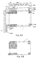
- Figs. 4A and 4B contain diagrammatic views of an LCD and Fig. 4A is a diagrammatic view of the LCD, and Fig. 4B is a diagrammatic view of a dot matrix of the display body or liquid crystal panel. A
display portion 1 of the liquid crystal panel is formed at a position where 200 horizontal scanning electrodes 2₁ - 2₂₀₀, and 640 signal electrodes 3₁ - 3₆₄₀ are crossed and consequently contains 200 x 640 dots. A scanningelectrodes driving circuit 4 supplies horizontal scanning signals X₁ - X₂₀₀ to the scanning electrodes 2₁ - 2₂₀₀. A signalelectrodes driving circuit 5 supplies data signals Y₁ - Y₆₄₀ to the signal electrodes 3₁ - 3₆₄₀. The signalelectrodes driving circuit 5 comprises 80 element circuits 5₁ - 5₈₀. Each element circuit is in charge of outputting the data signals Y for a respective group of 8 dots, i.e., afirst element circuit 5 outputs data signals Y₁ - Y₈, asecond element circuit 5₂ outputs data signals Y₉ - Y₁₆ and so on. Thus, in the device of Fig. 4A, the signalelectrodes driving circuit 5 having 80 element circuits 5₁ - 5₈₀ outputs a total of 640 data signals Y₁ - Y₆₄₀. - The scanning
electrodes driving circuit 4 repeatedly outputs horizontal scanning signals sequentially from X₁ to X₂₀₉. There are no scanning electrodes 2₂₀₁ - 2₂₀₉ corresponding to the scanning signals X₂₀₁ - X₂₀₉. Accordingly the effective area of the panel, i.e., the area of the panel where an image can be displayed comprises 200 dots in the vertical direction of the panel. Thedisplay portion 1 provided by the LCD of Fig. 4A can thus be represented as in a dot matrix shown in Fig. 4B. That is, thedisplay portion 1 has a size of 640 dots, i.e., 80 times 8-dot elements in the horizontal direction, and 200 dots in the vertical direction. In designing LCDs for image displays for practical uses in, e.g., personal computers, etc., it is preferable that two sheets of 200 dots x 640 dots panels are used to provide a 400 dots x 640 dots display body. - Fig. 5 shows the detailed structure of the
element circuits 5 of Fig. 4A. - As seen in Fig. 5, the element circuit comprises a
gradation data decoder 6, an effective dotmatrices generating circuit 7, and an output gate circuit having eight gate units GT₁ - GT₈. Thegradation decoder 6 decodes a color signal of 3 bits, R and G (most significant bits) and B (least significant bit) to supply an effective signal to one of output terminals 0 - 7 for outputting gradation signals, i.e., to place the output terminal in the state "1". The output terminal forGradation 0 is open, and when the gradation is 0, the data signals Y₁ - Y₈ are always 0. The output terminal forGradation 7 is directly connected to an OR gate of the output gate circuit, and when the gradation is 7, the data signals Y₁ - Y₈ are always "1", i.e., effective. For Gradations 1 - 6, lighting control for the respective dots is required. The effective dotmatrices generating circuit 7 conducts this control. - The effective dot
matrices generating circuit 7 has effective dot matrix generating circuit units 7₁ - 7₆ for the respective gradations which generate effective dot matrices for Gradations 1 - 6, and output signals from the terminals indicated by A - H,A -H are supplied to the output gate circuit. The eight gate units GT₁ - GT₈ of the output gate circuit correspond to the data signals Y₁ - Y₈. The respective gate units GT₁ - GT₈ are supplied with gradation outputs from thegradation data decoder 6 and output signals from the A - H output terminals and theA -H output terminals of the effective dotmatrices generating circuit 7. When the output signals of the output terminals A - H andA -H are "1", effective dot signals are obtained. - An output for
Gradation 1 of thegradation data decoder 6 is supplied to an AND gate gt₁ of the respective gate units GT₁ - GT₈, an output forGradation 2 to an AND gate gt₂, an output forGradation 3 to an AND gate gt₃,...., and an output forGradation 6 to an AND gate gt₆ of the respective gate units GT₁ - GT₈. The outputs A - H of the effective dotmatrix generating unit 7₁ forGradation 1 are supplied to the AND gates gt₁ of the respective gate units GT₁ - GT₈ in the sequential order of 1, 4, 6, 3, 5, 8, 2, 7 from the top as indicated in Fig. 5. In other words, the outputs of the output terminals A - H of the effective dotmatrix generating circuit 7₁ are supplied to the respective AND gates in combinations of A = GT₁, B = GT₄, C = GT₆, D = GT₃, E = GT₅, F = GT₈, G = GT₂ and H = GT₇. The outputs of the output terminals A - E of the effective dot matrix generating unit 7₂ forGradation 2 are supplied to the respective AND gate units gt₂ in combinations of A = GT₁, B = GT₃, GT₇, C = GT₅, D= GT₂, GT₈ , E = GT₄, GT₆. The outputs of the output terminals A - C of the effective dotmatrix generating unit 7₃ forGradation 3 are supplied to the respective AND gate units gt₃ in combinations of A = GT₂, GT₃, GT₇, B = GT₂, GT₆, C = GT₄, GT₈. The outputs forGradation 4 are supplied in the same combinations as forGradation 3. Those forGradation 5 are supplied in the same combinations as forGradation 2. Those forGradation 6 are supplied in the same combinations as forGradation 1. The outputs of the output terminalsA -H are supplied to the gate units GT₁ - GT₈. For example, the outputs of the output terminalsA -H , are supplied to the AND gates gt₆ of the respective gate units GT₁ - GT₈ in the sequential order of 1, 4, 6, 3, 5, 8, 2, 7 from the top. These input combinations determine distributions of effective dots in the horizontal and the vertical directions as shown in Fig. 3. - Fig. 6 shows in more detail the effective dot
matrices generating circuit 7. - As shown, the effective dot
matrices generating circuit 7 comprises a D-flip-flop 71, three OR gates 72₁ - 72₃ for receiving an outputQ of the D-flip-flop 71, three shift registers 73₁ - 73₃ each having an input terminal IN and eight output terminals corresponding to the output terminals A - H, and totally sixteen inverters 74₁ - 74₃. The effective dotmatrices generating circuit 7 is characteri zed in that the output terminal H of theshift register 73₁ is connected to theOR gate 72₁ so that eight signal outputs of the output terminals A - H are repeated many times. The output terminal E of theshift register 73₂ is connected to theOR gate 72₂ so that 5 signal outputs of the output terminals A - E are repeated many times. The output terminal C of theshift register 73₃ is connected to theOR gate 72₃ so that 3 output signals of the output terminal A - C are repeated many times. Thecircuit 7 is also characterized in that the inverters 74₁ - 74₃ are provided on the output side of the shift registers 73₁ - 73₃, which are respectively used commonly by circuits forGradations Gradations Gradations shift register 73₁supply 8 effective signals of the output terminals A - H forGradation 1, and by passing the 8 effective signals A - H through theinverter A -H forGradation 6 are obtained. Similarly from the output terminals of theshift register Gradation 2 are obtained, from the output terminals of theshift register 73₃, effective signal A - C are obtained, and by passing the 5 effective signals through theinverters A -E forGradations 5 and effective signalsA -C forGradation 4 are obtained. - In this embodiment, as described above, a 640 dots x 200 dots liquid crystal panel is used. Effective dot matrices are repeated 80 times in the horizontal direction. When a repetition cycle on turning of the dots in the vertical direction i.e., a repetition cycle of a horizontal scanning line, is a multiple of 8, 5 and 3 which are vertical sizes of the effective dot matrices, positions of the effective dots are fixed in every frame. Therefore, the scanning line has to be repeated in a cycle other than the above-descri bed multiples and larger than 200. That is, it is necessary that a vertical scanning signal is outputted every certain number of horizontal scanning signals, such as 202, 203, 206, 209, 211, 213, etc. But since more than 201 horizontal scannings are wasteful in the image display, it is preferable that the repetition cycle number is as small as possible.
- In this embodiment, when the horizontal scanning signal has been outputted 209 times, that is, the horizontal scanning signal X₂₀₉ is outputted, the vertical scanning signal is outputted, and then the horizontal scanning signal returns to the horizontal scanning signal X₁. It takes principally the least common multiple, or 8 x 5 x 3 frames = 120 frames for an effective dot distribution pattern to return to its initial pattern. In contrast to this, conventionally 8 dots x 8 dots effective dot matrices are set for respective gradations, and accordingly effective dots interfere with one another in every frame. But in this invention, the interferences are lessened to once 120 frames, with a result that gradation display is made more effective.
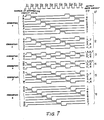
- Next, the operation of the embodiment of Figs. 4 - 6 will be explained with reference to Figs. 7 and 8.
- Fig. 7 is a timing chart of the operation of the above-described LCD. In Fig. 7, A - H and
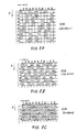
A -H represent output terminals of the effective dot matrix generating units 7₁ - 7₆ of Fig. 5 for generating effective dot matrices, and correspond to the output terminals of the shift registers 73₁ - 73₃, and to the output terminals of the inverters 74₁ - 74₃. When the output terminals A - H andA -H are in the state "1", effective signals for lighting dots are obtained. X₁ - X₁₂ represent horizontal scanning signals. This timing chart shows that the shift registers 73₁ - 73₃ are reset to shift the outputs of the effective signals sequentially from A -> B -> C -> .. every time a horizontal scanning signal is supplied to their respective terminals CK. - Fig. 8 shows effective dots obtained when the circuits of Fig. 4 - 6 are operated based on the signals of Fig. 7. Fig. 8A is for
Gradation 1, Fig. 8B is forGradation 2, and Fig. 8C is forGradation 3. In Fig. 8, the circles indicate effective dots in a first frame, the triangles indicate effective dots in a following second frame, and the crosses indicate effective dots in a third frame following the second one. - First, when the horizontal scanning signals X₁ - X₈ are sequentially outputted as shown in Fig. 7, the output terminals A - H of the effective dot
matrix generating unit 7₁ forGradation 1 become sequentially "1", i.e., have an effective signal. Then, since the output terminals A - H are connected to the respective gate units GT₁ - GT₈ in the sequential order of 1, 4, 6, 3, 5, 8, 2, 7 from the top as shown in Fig. 6, the effective dots are at X = 1 - 8, Y = 1, 4, 6, 3, 5, 8, 2, 7 as indicated by the circles in Fig. 8A. This operation is repeated. As shown in Fig. 4A, the scanningelectrodes driving circuit 4 has output terminals for the horizontal scanning signals X₁ - X₂₀₉, but thedisplay body 1 has only 200 scanning electrodes 2₁ - 2₂₀₀. Accordingly, the 8 dots x 8 dots effective dot matrix forGradation 1 is repeated 26 times a frame. In the next frame, the effective dots are shifted by one dot as indicated by the triangles in Fig. 8A, and in the frame after the next frame the effective dots are shifted further by one dot as indicated by the crosses in Fig. 8A. This is understood from thecalculation 209 = 8 x 26 + 1. - This explanation is for an 8 dots x 8 dots effective dot matrix for
Gradation 1. ForGradation 2, the effective dot matrix is 8 dots x 5 dots. Accordingly the effective dot matrix is repeated 41 times a frame. In the next frame, effective dots are shifted by 4 dots as indicated by the triangles in Fig. 8B, and in the frame following said next frame the effective dots are further shifted by 4 dots as indicated by the crosses in Fig. 8B. This is understood from thecalculation 209 = 5 x 41 + 4. The effective dot matrix forGradation 3 is repeated 69 times a frame. In the next frame, the effective dots are shifted by 2 dots as indicated by the triangles in Fig. 8C, and in the frame following said next frame the effective dots are further shifted by 2 dots as indicated by the crosses in Fig. 8C. This is understood from thecalculation 209 = 3 x 69 + 2. - In this embodiment, as shown in Fig. 7, effective dots are scattered in the horizontal and the vertical directions, are positioned at some places along the vertical and the horizontal lines, and are adjacent to one another in neither one frame nor a next frame. Consequently the fringe phenomenon becomes less conspicuous, and the interference is lessened. Gradation display is made much more effective.
- Fig. 9 shows another example explaining the same effect of Fig. 8A. The outputs of the output terminals A - H of the shift registers 72₁ - 72₃ are distributed in the horizontally sequential order of 1, 4, 7, 2, 5, 8, 3, 6. In this case as well, effective dots are not adjacent to one another in one frame, and in a next frame they do not become adjacent to one another.
- In the above-described embodiment, the driving circuits are in positive logic but can attain the same advantageous effect in negative logic.
Claims (9)
display means having a number of dots for displaying an image which are formed in a matrix at the crossing points of a plurality of signal electrodes (3₁-3₆₄₀) parallel with each other and a plurality of scanning electrodes (2₁-2₂₀₀) parallel with each other;
scanning electrodes driving means (4) for supplying scanning signals to the respective scanning electrodes in a sequential order;
signal electrodes driving means (5) for supplying data signals to the respective signal electrodes; and
electrode driving means for making the dots at those of the crossed positions where the scanning signals and the data signals meet effective for display an image,
the signal electrodes driving means (5) comprising:
gradation data output means (6) for outputting gradation data for instructing gradations of an image to be displayed in the unit of dot;
effective dot matrices generating means (7) for generating the effective dot matrix a distribution of the effective dots is based on and outputs effective signals for generating the effective dot matrix in more than two kinds of sizes which are different in the direction of row of the scanning electrodes in accordance with a gradation; and
output gate means (GT₁-GT₈) for outputting data signals for making the dots effective based on outputs of the gradation data output means and of the effective dot matrices generating means.
Applications Claiming Priority (6)
| Application Number | Priority Date | Filing Date | Title |
|---|---|---|---|
| JP3972589 | 1989-02-20 | ||
| JP39725/89 | 1989-02-20 | ||
| JP9911489 | 1989-04-19 | ||
| JP99114/89 | 1989-04-19 | ||
| JP1298842A JPH0361924A (en) | 1989-02-20 | 1989-11-17 | Method for controlling multi-gradation display body |
| JP298842/89 | 1989-11-17 |
Publications (3)
| Publication Number | Publication Date |
|---|---|
| EP0384403A2 true EP0384403A2 (en) | 1990-08-29 |
| EP0384403A3 EP0384403A3 (en) | 1991-03-20 |
| EP0384403B1 EP0384403B1 (en) | 1994-09-21 |
Family
ID=27290246
Family Applications (1)
| Application Number | Title | Priority Date | Filing Date |
|---|---|---|---|
| EP90103253A Expired - Lifetime EP0384403B1 (en) | 1989-02-20 | 1990-02-20 | A method for controlling a multi-gradation display and a multi-gradation display device |
Country Status (3)
| Country | Link |
|---|---|
| EP (1) | EP0384403B1 (en) |
| KR (1) | KR940001358B1 (en) |
| DE (1) | DE69012607T2 (en) |
Cited By (6)
| Publication number | Priority date | Publication date | Assignee | Title |
|---|---|---|---|---|
| EP0494826A1 (en) * | 1991-01-11 | 1992-07-15 | Commissariat A L'energie Atomique | Method for displaying images with Q grey levels on a matrix screen |
| EP0623912A1 (en) * | 1993-05-05 | 1994-11-09 | Philips Electronique Grand Public | Method and apparatus for the generation of gray scale levels in a passive matrix liquid crystal display |
| US5400044A (en) * | 1990-06-29 | 1995-03-21 | Acorn Computers Limited | Method and apparatus for producing grey levels on a raster scan video display device |
| US5489918A (en) * | 1991-06-14 | 1996-02-06 | Rockwell International Corporation | Method and apparatus for dynamically and adjustably generating active matrix liquid crystal display gray level voltages |
| WO1997008678A1 (en) * | 1995-08-25 | 1997-03-06 | S3, Incorporated | Frame rate control grayscale shading for liquid crystal display panels |
| EP1434195A1 (en) * | 2001-09-14 | 2004-06-30 | NEC Corporation | Image processing apparatus, image transmission apparatus, image reception apparatus, and image processing method |
Citations (5)
| Publication number | Priority date | Publication date | Assignee | Title |
|---|---|---|---|---|
| WO1984003577A1 (en) * | 1983-03-01 | 1984-09-13 | Tadeusz Bobak | Display device |
| EP0193728A2 (en) * | 1985-03-08 | 1986-09-10 | Ascii Corporation | Display control system |
| JPS62244018A (en) * | 1986-04-17 | 1987-10-24 | Seiko Epson Corp | Liquid crystal display element |
| JPS63287828A (en) * | 1987-05-20 | 1988-11-24 | Hitachi Ltd | Liquid crystal display controller |
| WO1989004505A1 (en) * | 1987-11-13 | 1989-05-18 | Honeywell Inc. | Apparatus and method for providing a gray scale in liquid crystal flat panel displays |
-
1990
- 1990-02-16 KR KR1019900001878A patent/KR940001358B1/en active IP Right Grant
- 1990-02-20 EP EP90103253A patent/EP0384403B1/en not_active Expired - Lifetime
- 1990-02-20 DE DE69012607T patent/DE69012607T2/en not_active Expired - Lifetime
Patent Citations (5)
| Publication number | Priority date | Publication date | Assignee | Title |
|---|---|---|---|---|
| WO1984003577A1 (en) * | 1983-03-01 | 1984-09-13 | Tadeusz Bobak | Display device |
| EP0193728A2 (en) * | 1985-03-08 | 1986-09-10 | Ascii Corporation | Display control system |
| JPS62244018A (en) * | 1986-04-17 | 1987-10-24 | Seiko Epson Corp | Liquid crystal display element |
| JPS63287828A (en) * | 1987-05-20 | 1988-11-24 | Hitachi Ltd | Liquid crystal display controller |
| WO1989004505A1 (en) * | 1987-11-13 | 1989-05-18 | Honeywell Inc. | Apparatus and method for providing a gray scale in liquid crystal flat panel displays |
Non-Patent Citations (2)
| Title |
|---|
| PATENT ABSTRACTS OF JAPAN vol. 12, no. 114 (P-688), 12 April 1988; & JP - A - 62244018 (SEINO EPSON) 24.10.1987 * |
| PATENT ABSTRACTS OF JAPAN vol. 13, no. 112 (P-844), 17 March 1989; & JP - A - 63287828 (HITACHI) 24.11.1988 * |
Cited By (9)
| Publication number | Priority date | Publication date | Assignee | Title |
|---|---|---|---|---|
| US5400044A (en) * | 1990-06-29 | 1995-03-21 | Acorn Computers Limited | Method and apparatus for producing grey levels on a raster scan video display device |
| EP0494826A1 (en) * | 1991-01-11 | 1992-07-15 | Commissariat A L'energie Atomique | Method for displaying images with Q grey levels on a matrix screen |
| FR2671656A1 (en) * | 1991-01-11 | 1992-07-17 | Commissariat Energie Atomique | DISPLAY PROCESS ON A MATRIX SCREEN OF IMAGES INCLUDING Q GRAY LEVELS. |
| US5321418A (en) * | 1991-01-11 | 1994-06-14 | Commissariat A L'energie Atomique | Method for displaying images comprising Q levels of grey on a matrix screen |
| US5489918A (en) * | 1991-06-14 | 1996-02-06 | Rockwell International Corporation | Method and apparatus for dynamically and adjustably generating active matrix liquid crystal display gray level voltages |
| EP0623912A1 (en) * | 1993-05-05 | 1994-11-09 | Philips Electronique Grand Public | Method and apparatus for the generation of gray scale levels in a passive matrix liquid crystal display |
| WO1997008678A1 (en) * | 1995-08-25 | 1997-03-06 | S3, Incorporated | Frame rate control grayscale shading for liquid crystal display panels |
| EP1434195A1 (en) * | 2001-09-14 | 2004-06-30 | NEC Corporation | Image processing apparatus, image transmission apparatus, image reception apparatus, and image processing method |
| EP1434195A4 (en) * | 2001-09-14 | 2009-01-21 | Nec Corp | Image processing apparatus, image transmission apparatus, image reception apparatus, and image processing method |
Also Published As
| Publication number | Publication date |
|---|---|
| DE69012607T2 (en) | 1995-03-23 |
| KR940001358B1 (en) | 1994-02-19 |
| DE69012607D1 (en) | 1994-10-27 |
| EP0384403A3 (en) | 1991-03-20 |
| EP0384403B1 (en) | 1994-09-21 |
| KR900013441A (en) | 1990-09-05 |
Similar Documents
| Publication | Publication Date | Title |
|---|---|---|
| US5196839A (en) | Gray scales method and circuitry for flat panel graphics display | |
| US8199102B2 (en) | Liquid crystal display and method of driving the same utilizing data line blocks | |
| CN101533630B (en) | Driving method of deplay device having main display and sub display | |
| US5172108A (en) | Multilevel image display method and system | |
| US5252959A (en) | Method and apparatus for controlling a multigradation display | |
| CN102378031B (en) | Electro-optical device and electronic equipment | |
| JPH032722A (en) | Driving method for display device | |
| JPS6019196A (en) | Method and apparatus for driving liquid crystal display | |
| EP1410374B1 (en) | Display driver apparatus and driving method | |
| EP0384403A2 (en) | A method for controlling a multi-gradation display and a multi-gradation display device | |
| US6972779B2 (en) | Flat-panel display device | |
| KR20020082417A (en) | Display device and method of driving the same | |
| JP2823614B2 (en) | Gradation display method and liquid crystal display device | |
| JP3426723B2 (en) | Liquid crystal display device and driving method thereof | |
| CA2164803C (en) | Method and circuit for driving picture display devices | |
| EP0260146A2 (en) | Multi-colour display system | |
| CN111341235B (en) | Display panel's drive arrangement and display device | |
| US6081252A (en) | Dispersion-based technique for performing spacial dithering for a digital display system | |
| KR100982083B1 (en) | Liquid crystal display device | |
| JPH10161610A (en) | Liquid crystal display unit | |
| JPH03130797A (en) | Display controller | |
| EP1341150A1 (en) | Method for driving LCD modules with scale of greys by PWM technique and reduced power consumption | |
| JP2641778B2 (en) | Color liquid crystal display device | |
| CN200947341Y (en) | Display controller for producing multiple light-shade level image | |
| JP3165478B2 (en) | Driving method of color display device |
Legal Events
| Date | Code | Title | Description |
|---|---|---|---|
| PUAI | Public reference made under article 153(3) epc to a published international application that has entered the european phase |
Free format text: ORIGINAL CODE: 0009012 |
|
| AK | Designated contracting states |
Kind code of ref document: A2 Designated state(s): DE FR GB |
|
| PUAL | Search report despatched |
Free format text: ORIGINAL CODE: 0009013 |
|
| AK | Designated contracting states |
Kind code of ref document: A3 Designated state(s): DE FR GB |
|
| 17P | Request for examination filed |
Effective date: 19910315 |
|
| 17Q | First examination report despatched |
Effective date: 19930423 |
|
| GRAA | (expected) grant |
Free format text: ORIGINAL CODE: 0009210 |
|
| AK | Designated contracting states |
Kind code of ref document: B1 Designated state(s): DE FR GB |
|
| REF | Corresponds to: |
Ref document number: 69012607 Country of ref document: DE Date of ref document: 19941027 |
|
| ET | Fr: translation filed | ||
| PLBE | No opposition filed within time limit |
Free format text: ORIGINAL CODE: 0009261 |
|
| STAA | Information on the status of an ep patent application or granted ep patent |
Free format text: STATUS: NO OPPOSITION FILED WITHIN TIME LIMIT |
|
| 26N | No opposition filed | ||
| REG | Reference to a national code |
Ref country code: GB Ref legal event code: IF02 |
|
| PGFP | Annual fee paid to national office [announced via postgrant information from national office to epo] |
Ref country code: DE Payment date: 20090213 Year of fee payment: 20 |
|
| PGFP | Annual fee paid to national office [announced via postgrant information from national office to epo] |
Ref country code: GB Payment date: 20090217 Year of fee payment: 20 |
|
| PGFP | Annual fee paid to national office [announced via postgrant information from national office to epo] |
Ref country code: FR Payment date: 20090213 Year of fee payment: 20 |
|
| REG | Reference to a national code |
Ref country code: GB Ref legal event code: PE20 Expiry date: 20100219 |
|
| PG25 | Lapsed in a contracting state [announced via postgrant information from national office to epo] |
Ref country code: GB Free format text: LAPSE BECAUSE OF EXPIRATION OF PROTECTION Effective date: 20100219 |
|
| PG25 | Lapsed in a contracting state [announced via postgrant information from national office to epo] |
Ref country code: DE Free format text: LAPSE BECAUSE OF EXPIRATION OF PROTECTION Effective date: 20100220 |