EP0386965A1 - Optically powered sensor arrangements - Google Patents
Optically powered sensor arrangements Download PDFInfo
- Publication number
- EP0386965A1 EP0386965A1 EP90302278A EP90302278A EP0386965A1 EP 0386965 A1 EP0386965 A1 EP 0386965A1 EP 90302278 A EP90302278 A EP 90302278A EP 90302278 A EP90302278 A EP 90302278A EP 0386965 A1 EP0386965 A1 EP 0386965A1
- Authority
- EP
- European Patent Office
- Prior art keywords
- arrangement according
- capacitance
- optical
- pulse
- pulses
- Prior art date
- Legal status (The legal status is an assumption and is not a legal conclusion. Google has not performed a legal analysis and makes no representation as to the accuracy of the status listed.)
- Granted
Links
Images

Classifications
-
- G—PHYSICS
- G01—MEASURING; TESTING
- G01F—MEASURING VOLUME, VOLUME FLOW, MASS FLOW OR LIQUID LEVEL; METERING BY VOLUME
- G01F23/00—Indicating or measuring liquid level or level of fluent solid material, e.g. indicating in terms of volume or indicating by means of an alarm
- G01F23/22—Indicating or measuring liquid level or level of fluent solid material, e.g. indicating in terms of volume or indicating by means of an alarm by measuring physical variables, other than linear dimensions, pressure or weight, dependent on the level to be measured, e.g. by difference of heat transfer of steam or water
- G01F23/26—Indicating or measuring liquid level or level of fluent solid material, e.g. indicating in terms of volume or indicating by means of an alarm by measuring physical variables, other than linear dimensions, pressure or weight, dependent on the level to be measured, e.g. by difference of heat transfer of steam or water by measuring variations of capacity or inductance of capacitors or inductors arising from the presence of liquid or fluent solid material in the electric or electromagnetic fields
- G01F23/263—Indicating or measuring liquid level or level of fluent solid material, e.g. indicating in terms of volume or indicating by means of an alarm by measuring physical variables, other than linear dimensions, pressure or weight, dependent on the level to be measured, e.g. by difference of heat transfer of steam or water by measuring variations of capacity or inductance of capacitors or inductors arising from the presence of liquid or fluent solid material in the electric or electromagnetic fields by measuring variations in capacitance of capacitors
- G01F23/266—Indicating or measuring liquid level or level of fluent solid material, e.g. indicating in terms of volume or indicating by means of an alarm by measuring physical variables, other than linear dimensions, pressure or weight, dependent on the level to be measured, e.g. by difference of heat transfer of steam or water by measuring variations of capacity or inductance of capacitors or inductors arising from the presence of liquid or fluent solid material in the electric or electromagnetic fields by measuring variations in capacitance of capacitors measuring circuits therefor
-
- G—PHYSICS
- G01—MEASURING; TESTING
- G01D—MEASURING NOT SPECIALLY ADAPTED FOR A SPECIFIC VARIABLE; ARRANGEMENTS FOR MEASURING TWO OR MORE VARIABLES NOT COVERED IN A SINGLE OTHER SUBCLASS; TARIFF METERING APPARATUS; MEASURING OR TESTING NOT OTHERWISE PROVIDED FOR
- G01D5/00—Mechanical means for transferring the output of a sensing member; Means for converting the output of a sensing member to another variable where the form or nature of the sensing member does not constrain the means for converting; Transducers not specially adapted for a specific variable
- G01D5/12—Mechanical means for transferring the output of a sensing member; Means for converting the output of a sensing member to another variable where the form or nature of the sensing member does not constrain the means for converting; Transducers not specially adapted for a specific variable using electric or magnetic means
- G01D5/14—Mechanical means for transferring the output of a sensing member; Means for converting the output of a sensing member to another variable where the form or nature of the sensing member does not constrain the means for converting; Transducers not specially adapted for a specific variable using electric or magnetic means influencing the magnitude of a current or voltage
- G01D5/24—Mechanical means for transferring the output of a sensing member; Means for converting the output of a sensing member to another variable where the form or nature of the sensing member does not constrain the means for converting; Transducers not specially adapted for a specific variable using electric or magnetic means influencing the magnitude of a current or voltage by varying capacitance
- G01D5/2405—Mechanical means for transferring the output of a sensing member; Means for converting the output of a sensing member to another variable where the form or nature of the sensing member does not constrain the means for converting; Transducers not specially adapted for a specific variable using electric or magnetic means influencing the magnitude of a current or voltage by varying capacitance by varying dielectric
Definitions
- the invention relates to optically powered sensor arrangements. Such arrangements may be used for sensing physical parameters.
- optical energy from a source may be supplied to one or more sensors which, in turn, provide information-bearing optical energy representative of the sensed parameter.
- Various types of sensors and sensor arrangements are known for measuring physical parameters.
- electrical sensors which provide a variation in resistance, capacitance, or other electrical characteristic as a function of a sensed physical parameter have been used to provide an electrical current or voltage output.
- the resistance of a thermistor varies as a function of its temperature and can be used in a simple bridge circuit to provide a temperature responsive output current.
- capacitors and capacitor-like structures can be used to provide electrical signal outputs which are responsive to environmental parameters affecting the dielectric constant of the capacitor.
- groups of sensors are typically interconnected with a controller which provides electrical power to the various sensors and measures or otherwise senses the parameter-affected electrical characteristic.
- electrical sensors and electrical interconnections represent highly developed and reliable technology, although unshielded systems can be subject to electromagnetic interference (EMI).
- EMI electromagnetic interference
- Optical fibre transmission is best suited to digitally encoded optical pulses in which the information to be conveyed is encoded by varying an attribute of the pulse, such as the pulse width, amplitude, or repetition rate.
- systems which transmit analog light signals through optical fibres are less than optimal because of the substantial variation in attenuation for the transmitted energy as a consequence of the fibre temperature, external pressure applied to the fibre, the presence of small-radius bends in the fibre, and the cumulative effects of defects in the fibre.
- optical energy is transmitted via optical fibres to a sensor which includes a photodetector and a storage capacitor for converting the input optical energy to electricity for storage in the capacitor.
- a transducer such as a temperature sensor, uses the stored electrical energy to provide an electrical output to a pulse width modulator, such as a light-emitting diode or a laser diode, to transmit one or more return pulses indicative of the measured parameter.
- a pulse width modulator such as a light-emitting diode or a laser diode
- the use of pulse width modulation requires that the light emitting diode or laser diode be powered during the transmission of the entire pulse.
- the optical energy emitter can consume the major portion of the available stored energy and represent a constraint to efficient operation.
- the information is provided using short-duration optical spikes which consume less power for the volume of information transferred. Additionally, at least one spike of the transmitted spikes is representative of a fixed-value reference so that each information-bearing spike can be evaluated in relationship to its associated reference spike to provide improved overall accuracy.
- an optically powered sensor arrangement comprising a receiving device for receiving transmitted optical energy and converting it into electrical energy, and a storage device for storing the electrical energy, and characterised by a transducing device having a characteristic whose value varies as a function of a parameter to be sensed, a reference device having the same characteristic but whose value is independent of the parameter to be sensed, and a circuit device energised by the electrical energy stored in the storage device for comparing the two values of the characteristic so as to produce a multi-pulse output having a first time attribute which is a function of the value of the characteristic of the transducing device and a second time attribute which is a function of the value of the characteristic of the reference device.
- the optically powered sensor arrangement to be described has improved signal conditioning for measuring various parameters and provides an optical signal representative of the measured parameter.
- the optically powered arrangement includes at least one sensor having a power converter for converting optical energy to electrical energy for storage in an electrical storage device, such as a capacitor, associated with the sensor.
- a transducer such as a capacitor or thermistor having a characteristic that varies as a function of the sensed parameter, and a reference unit, such as a fixed-value capacitor or resistor, is associated with each sensor.
- the transducer and the reference control an integrator in a pulse encoder to provide output electrical pulses which are a function of the fixed-value reference and the parameter-affected measured value.
- the pulse output drives an optical energy source to provide optical pulses having an attribute representative of the fixed-value reference and the parameter-affected value of the transducer.
- a plurality of sensors are connected to a system optical bus which communicates with a microprocessor controlled system controller.
- the system controller transmits optical energy along the bus for system-wide distribution to all sensors in the system and receives return pulses from the various sensors, the return pulses including information as to the measured parameter sensed by the sensor and to a sensor-specific reference value.
- Each sensor includes a photodiode array for converting optical energy transmitted system-wide by the controller into electrical energy for storage in a capacitor associated with each sensor.
- a transducer in the form of a capacitance probe and a fixed-value reference capacitor are connected to an integrator within the pulse encoder.
- the integrator In response to power switched from the storage capacitor and under the control of a timing and sequence controller, the integrator provides a recurring sequence of ramp outputs with a first ramp output varying as a function of the capacitance of the capacitance probe in response to the measured parameter and a second ramp output which varies as a function of the combined or cumulative capacitance of the capacitance probe and the fixed-value reference capacitance.
- Each ramp output is provided to a pair of comparators which trigger respective one-shots at respective lower and upper value limits to provide a pair of time-spaced short-duration pulses that are a function of the parameter-affected capacitance of the capacitance probe and the combined or cumulative capacitance of the capacitance probe and the capacitance of the fixed-value reference.
- the short-duration pulses are used to drive an optical source for transmitting corresponding short-duration optical pulses from the sensor to the system controller.
- each sensor is provided with sensor-specific time delay prior to the transmission of return pulses from the sensor to the system controller to allow a predetermined 'time window' for each of the sensors to effect transmission to the central controller.
- the various sensors of the system thus transmit return pulses in a predetermined time-multiplexed sequence.
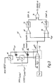
- the optically powered sensor arrangement now to be more specifically described is shown in schematic form in Figure 1 and is designated generally therein by the reference character 10.
- a plurality of sensors S0,S1,...S n-1 , S n are connected by respective optical fibres f0, 1, ... f n-1 , f n to a distribution coupler 12, which, in turn, is connected to another coupler 14 through an optical fibre bus 16.
- the coupler 14 is designed to distribute optical energy from the bus 16 to the respective sensors S n and, conversely, direct optical energy from the sensors S n along the bus 16 to the coupler 14.
- the couplers 12 and 14 can take the form of star-type couplers or lateral couplings.
- a system controller 22 is connected to the optical source 18 and the optical receiver 20 and functions, as described below, to drive the optical source 18 to introduce optical energy into the system and to process the return signals from the optical receiver 20.
- the controller 22 includes a logic unit 24 which operates through a recurring cycle under the control of a clock 26 to provide current through a drive amplifier 28 to cause the optical source 18 to direct optical energy through the coupler 14 and the bus 16 to the coupler 12 and the various sensors S n .
- an amplifier 30 accepts pulse signals from the optical receiver 20 for presentation to the logic unit 24.
- the controller 22 operates under the general control of a micro-processor 32 with communication provided through a bus 34 and respective I/O ports.
- An output device 36 such as a multi-digit display, is connected to the microprocessor 32 and provides output information as to the parameters sensed by the sensors S n .
- each sensor S n includes a transducer 40 which has a characteristic, such as capacitance, which changes in a predictable manner with the sensed parameter.
- a pulse encoder 42 is connected to the transducer 40 and to a fixed-value reference 44 and provides a pulse output, as described more fully below, to an output driver 46 which, in turn, drives a light emitting diode 48 to provide optical pulses through the coupler 12 and the bus 16.
- the transducer 40 takes the form of a capacitance probe 40 used in fuel tank measurement systems in aircraft, and the fixed-value reference 44 takes the form of a precision fixed-value capacitance.
- the capacitance probes 40′ are typically fabricated from conductive cylindrical sleeves which are concentrically mounted relative each other to define capacitor plates. The probe 40′ is positioned within its fuel tank with the dielectric constant between the plates determined by the portion of the probe 40′ which is wetted by the fuel, as well as by the airspace above the fuel.
- an exemplary fuel tank T is shown in dotted line illustration as containing a liquid which can assume varying levels as represented by levels L1 and L2.
- Optical energy provided by the optical energy source 18 through the bus 16 and the coupler 12 is provided to a power converter 50 within each sensor S n which includes a series-connected array of photodiodes 52 in shunt circuit with a storage capacitor 54 and in series circuit with a diode 56.
- Optical energy provided through the bus 16 and the coupler 12 is converted to a DC potential by the photodiodes 52 and stored in the shunt-connected capacitor 54.
- the diode 56 has a low forward voltage drop and serves to isolate the photodiodes 52 from the remainder of the circuitry.
- a power switch 58 is connected to the power converter 50 and selectively provides power to the pulse encoder 42 under the control of a timing and sequence control circuit 60.
- the power switch 58 can take the form of a MOSFET or other gate-controlled device.
- One form of the integrating pulse encoder or modulator 42 is shown in Figure 3 and, as shown, includes an integrator 62 which functions to time-integrate a voltage V ref as a function of the capacitance C probe of the capacitance probe 40′ and as a function of the parallel-connected capacitance of the capacitance probe 40 and the capacitance of the reference 44, i.e., C probe + C ref .
- the integrator 62 may be defined by an operational amplifier, such as a Harris 5141 op-amp in a Miller integrator or functionally equivalent configuration.
- the voltage V ref is supplied from the charge in the storage capacitor 54 and is quantitatively controlled by a regulator and/or zener diode circuit (not shown).
- the capacitance probe 40′ is connected in a feedback configuration between the output and the input of the integrator 62.
- the reference capacitor 44 is selectively connected in parallel with the capacitance probe 40′ through a switch 64 which is controlled by the timing and sequence control circuit 60 ( Figure 2).
- Another switch 66 is connected in shunt circuit with the reference capacitor 44 and the capacitance probe 40′ and is selectively operated by the timing and sequence control circit 60 for periodically resetting the integrator 62 by shunting both the capacitance probe 40′ and the reference capacitor 44, as explained below in relationship to Figures 4 and 5.
- the switches 64 and 66 can take the form of a MOSFET or other gate-controlled device.
- the integrator 62 provides a recurring ramp output having a rate-of-increase (i.e., slope) which is a function of the capacitance in its feedback loop, as represented in a qualitative graphical manner by the solid and dotted line inclines shown in Figure 3 at the output of the integrator 62.
- the ramp output of the integrator 62 is fed to a dual-comparator circuit which includes a first comparator 68 and a second comparator 70 configured to provide respective outputs when the ramp output of the integrator 62 exceeds predetermined lower and upper limits.
- the comparators 68 and 70 can be configured from high-gain operational amplifiers.
- the voltage divider defined by the series-connected resistors connected to the inverting input of the comparator 68 establishes an upper limit which is higher than that of the comparator 70.
- the output of each comparator 68 and 70 is fed, respectively, to one-shot monostable multivibrators 72 and 74.
- the one-shots 72 and 74 each provide a short-duration output pulse through an OR gate 76 to the driver 46 ( Figure 2), which, in turn, provides corresponding short-duration optical spikes.
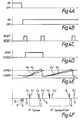
- the integrator 62 provides a sequence of recurring ramp outputs during each measurement cycle ( Figures 4A-4F) as a function of the capacitance in its feedback path.
- Comparators 70 and 68 trigger their respective one-shots 74 and 72 as the ramp value progressively exceeds the lower and then the upper limits.
- the interpulse spacing is, accordingly, representative of the parameter-affected capacitance in the feedback path of the integrator 62.
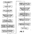
- the optically powered sensor system operates in accordance with the flow diagram of Figure 5 to sense the measured parameter and provide a pulse sequence, as shown in Figure 4F, containing information representative of the measured parameter as well as the reference value.
- the system is initialized by transmitting optical energy from the optical energy source 18 through the bus 16 for distribution to all sensors S n in the system.
- the photodiodes 52 of each sensor S n convert the distributed optical energy to an electric current and charge the storage capacitor 54 of each sensor S n , preferably to a full charge or near full charge condition as determined by the timing and sequence control circuit 60.
- the optical energy provided from the optical source 18 is of a sufficient duration and intensity to assure a sufficient charge in the capacitor 54 of each sensor S n for at least one measurement cycle.
- the distributed optical energy is halted at time T0 by the controller 22 in response to commands provided from the microprocessor 32.
- the termination of the distributed optical energy is detected by each sensor S n and the power switch 58 of each sensor S n switched at time T1 to apply power to the remaining sensor circuitry ( Figure 4B).
- the integrator 62 is reset by closing both the switches 64 and 66 to effectively shunt the feedback path of the integrator 62 for some time period between times T2 and T3, as represented in Figure 4C.
- the reset interval forces the output of the integrator 62 to a known initial voltage.
- the switch 64 is opened ( Figure 4D) in response to a command from the timing and sequence control circuit 60 to effectively leave only the capacitance probe 40′ and its capacitance C probe in the integrator 62 feedback loop.
- the reset switch 66 is opened by the timing and sequence control circuit 60 with the output of the integrator 62 rising in a ramp-like manner as the capacitance in the feedback path is charged.
- the slope of the output ramp is a function of the capacitance in the feedback path, a larger capacitance providing a lower slope as represented by the solid and dotted line ramps R1 and R1′ in Figure 4D.
- the ramp R1 value increases, it exceeds the lower limit established by the comparator 70 which changes its output state to trigger the one-shot 74 to produce a first short-duration output pulse P1 at time T P1 as shown in Figure 4F.
- the ramp R1 value continues to increase at a rate that is a function of the capacitance C probe in its feedback path until the ramp R1 value exceeds the upper limit established by the comparator 68 which then changes its output state to trigger the one-shot 72 to produce a second short-duration output pulse P2 at time T P2 .
- the time interval dT between time T P1 and time T P2 is a function of the value of the capacitance C probe of the probe 40′, and, in the case of the preferred application, will vary as a function of the level L of the liquid in the tank T ( Figure 2).
- a lower-slope ramp will exceed the lower limit established by the comparator 70 to produce a first pulse P 1′ , and a time T P1′ (as shown in dotted line illustration) somewhat later than the time T P1 in the case of the ramp R1.
- the comparator 68 will change its output state to trigger the one-shot 72 to produce the second pulse P2 (dotted line illustration) at time T P2′ .
- the time interval dT between times T P1 and time T P2 for the ramp R1 and the time interval between times T P1′ and time T P2′ for the ramp R1′ will differ as a function of the value of the capacitance C probe of the probe 40′ which is function of the level L of the liquid in the tank T ( Figure 2).
- the switch 64 is closed (as shown in Figure 4D) and the reset switch 66 is closed under the control of the timing and sequence control circuit 60 between times T4 and T5 so as again to reset the integrator 62 by effectively shunting the parallel-connected capacitances C probe and C ref .
- the reset switch 66 is opened by the timing and sequence control circuit 60. Since the switch 64 remains closed the combined capacitances C probe + C ref of the parallel-connected capacitance probe 40′ and the reference capacitor 44 are in the integrator 62 feedback path.
- the output of the integrator 62 rises again in a ramp-like manner, as indicated by the solid-line ramp R2, as the capacitance in the feedback path is charged. Since the parallel-connected capacitance C probe + C ref is greater than that of the capacitance C probe , the rate of increase of the ramp R2 occurring after time T5 will be lower than in the case of the ramp R1 occurring after time T3, although the ramp R2 will nonetheless be a function of the parameter-affected value of the capacitance C probe . As the ramp R2 value increases, it will exceed the lower limit established by the comparator 70 which changes its output state to trigger the one-shot 74 to produce a third short-duration output pulse P3 at time T P3 .
- the ramp R2 value will continue to increase at a rate that is a function of the capacitance C probe + C ref in its feedback path until the ramp R2 value exceeds the upper limit established by the comparator 68 which then changes its output state to trigger the one-shot 72 to produce a fourth short-duration output pulse P4 at time T P4 .
- a lower-slope ramp R′2 (dotted line illustration) will exceed the lower limit established by the comparator 70 to produce the first pulse P3′ at a time T P3 ′ (as shown in dotted line illustration) somewhat later than the time T P3 in the case of the ramp R2.
- the comparator 68 will change its output state to trigger the one-shot 72 to produce the second pulse P4′ (dotted line illustration) at time T P4′ .
- the integrator 62 is again reset as described above during an interval between times T6 and T7.
- the pulse encoder 42 of each sensor S n is provided with a sensor-specific time delay; thus a first sensor S1 functions to respond after a 450 microsecond period after time T1, the second sensor S2 functions to respond after a 900 microsecond period after time T1, the third sensor S3 functions to respond during a 1350 microsecond period after time T1, etc.
- This sensor-specific time delay prior to the transmission of the return pulses from the sensors to the system controller allows a predetermined 'time window' for each of the sensors S n to effect transmission to the system controller 22.
- the various sensors S n of the system thus transmit return pulses in a predetermined time-multiplexed sequence.
- the optical pulses P1, P2, P3, and P4 have a relatively short duration, that is, of the order of two to eight microseconds, and thus constitute optical spikes rather than pulses having an appreciable duration.
- the duration of the electrical pulse output of the one-shots 72 and 74 through the OR gate 76 ( Figure 3) is sufficient to drive the light emitting diode 48 to provide the short-duration optical pulses P1, P2, P3 and P4.
- the inclusion of the reference pulse information allows evaluation of the parameter-affected value in the context of a reference that is subjected to the same variables, i.e., the storage capacitor 54 and the related circuitry, so that errors introduced at the sensor S n by sub-optimal performance of the energy storage function, environmental factors, or ageing will be cancelled or effectively minimized.
- the optical pulses are returned to the system controller 22 ( Figure 1) from each sensor S n along the bus 16, and the micro-processor 32 processes the information by determining the time interval between times T P1 and time T P2 and times TP3 and TP4 and obtains a ratio of the first time interval relative to the second time interval and multiplies this ratio by the known value of the reference capacitor 44 and other system specific scale factors.
- the value of the measured parameter is thus obtained as a function of the reference value, and, accordingly, the measured value which is representative of the measured parameter is independent of the storage capacitor 54 used in each sensor S n and is also relatively immune related circuit drift.
- the system described advantageously provides improved signal conditioning in which the value of the measured parameter is obtained as a function of a reference value, and, accordingly, the measurement of the sensed parameter is independent of the energy storage device used in each sensor and is also relatively immune to component value drift.
- the use of short-duration optical pulses results in improved energy utilization in contrast to systems which use pulse width modulation.
Abstract
Description
- The invention relates to optically powered sensor arrangements. Such arrangements may be used for sensing physical parameters. In such arrangements, optical energy from a source may be supplied to one or more sensors which, in turn, provide information-bearing optical energy representative of the sensed parameter.
- Various types of sensors and sensor arrangements are known for measuring physical parameters. Traditionally, electrical sensors which provide a variation in resistance, capacitance, or other electrical characteristic as a function of a sensed physical parameter have been used to provide an electrical current or voltage output. For example, the resistance of a thermistor varies as a function of its temperature and can be used in a simple bridge circuit to provide a temperature responsive output current. In a similar manner, capacitors and capacitor-like structures can be used to provide electrical signal outputs which are responsive to environmental parameters affecting the dielectric constant of the capacitor. In a system or network context, groups of sensors are typically interconnected with a controller which provides electrical power to the various sensors and measures or otherwise senses the parameter-affected electrical characteristic. In general, electrical sensors and electrical interconnections represent highly developed and reliable technology, although unshielded systems can be subject to electromagnetic interference (EMI).
- With the advent of optical fibres, sensor systems using optical fibres to transmit information from one node in a network to another have been developed or proposed. Optical fibre transmission is best suited to digitally encoded optical pulses in which the information to be conveyed is encoded by varying an attribute of the pulse, such as the pulse width, amplitude, or repetition rate. However, systems which transmit analog light signals through optical fibres are less than optimal because of the substantial variation in attenuation for the transmitted energy as a consequence of the fibre temperature, external pressure applied to the fibre, the presence of small-radius bends in the fibre, and the cumulative effects of defects in the fibre.
- In view of the highly developed state of traditional electrical sensors and the advantages attendant on pulse transmission in optical fibres, an optimal system can be achieved using traditional electrical sensors with optical fibre interconnection. In general, however, the need to power the electrical sensors requires separate electrical power paths to the sensors and thus adds undesired complexity to the overall system.
- In one prior optical sensor system, as disclosed in U.S.-4 346 478 (Sichling), optical energy is transmitted via optical fibres to a sensor which includes a photodetector and a storage capacitor for converting the input optical energy to electricity for storage in the capacitor. A transducer, such as a temperature sensor, uses the stored electrical energy to provide an electrical output to a pulse width modulator, such as a light-emitting diode or a laser diode, to transmit one or more return pulses indicative of the measured parameter. While such prior system operates to provide duration-modulated pulses, the overall accuracy of the measurement is a function of the stored energy, and the accuracy can degrade with changing characteristics of the storage capacitor, as can occur, for example, with changes in temperature and component ageing. In addition, the use of pulse width modulation requires that the light emitting diode or laser diode be powered during the transmission of the entire pulse. In the context of low-power systems, the optical energy emitter can consume the major portion of the available stored energy and represent a constraint to efficient operation.
- In the system disclosed in co-pending U.S. Patent Application Serial No. 07/046,075, filed May 5, 1987 by D. Patriquin and entitled "Optically Powered Sensor System", the information is provided using short-duration optical spikes which consume less power for the volume of information transferred. Additionally, at least one spike of the transmitted spikes is representative of a fixed-value reference so that each information-bearing spike can be evaluated in relationship to its associated reference spike to provide improved overall accuracy.
- According to the invention, there is provided an optically powered sensor arrangement, comprising a receiving device for receiving transmitted optical energy and converting it into electrical energy, and a storage device for storing the electrical energy, and characterised by a transducing device having a characteristic whose value varies as a function of a parameter to be sensed, a reference device having the same characteristic but whose value is independent of the parameter to be sensed, and a circuit device energised by the electrical energy stored in the storage device for comparing the two values of the characteristic so as to produce a multi-pulse output having a first time attribute which is a function of the value of the characteristic of the transducing device and a second time attribute which is a function of the value of the characteristic of the reference device.
- Optically powered sensor arrangements embodying the invention will now be described, by way of example only, with reference to the accompanying drawings in which:-
- Figure 1 is an overall schematic diagram of one of the optical sensor arrangements;
- Figure 2 is a schematic block diagram of one of the sensors in the arrangement of Figure 1;
- Figure 3 is a functional block diagram of an integrating pulse encoder for providing pulses having attributes representative of a measured value and a reference value and for use in the sensor arrangement of Figure 1;
- Figures 4A to 4F are idealized timing charts graphically illustrating the sequence of operations for the sensor arrangement of Figure 1; and
- Figure 5 is a flow diagram of the control sequence for the sensor arrangement of Figure 1 to obtain the measured-value and reference-value pulses of Figures 4A to 4F.
- The optically powered sensor arrangement to be described has improved signal conditioning for measuring various parameters and provides an optical signal representative of the measured parameter. The optically powered arrangement includes at least one sensor having a power converter for converting optical energy to electrical energy for storage in an electrical storage device, such as a capacitor, associated with the sensor. A transducer, such as a capacitor or thermistor having a characteristic that varies as a function of the sensed parameter, and a reference unit, such as a fixed-value capacitor or resistor, is associated with each sensor. The transducer and the reference control an integrator in a pulse encoder to provide output electrical pulses which are a function of the fixed-value reference and the parameter-affected measured value. The pulse output, in turn, drives an optical energy source to provide optical pulses having an attribute representative of the fixed-value reference and the parameter-affected value of the transducer.
- In a preferred arrangement to be described in detail, a plurality of sensors are connected to a system optical bus which communicates with a microprocessor controlled system controller. The system controller transmits optical energy along the bus for system-wide distribution to all sensors in the system and receives return pulses from the various sensors, the return pulses including information as to the measured parameter sensed by the sensor and to a sensor-specific reference value. Each sensor includes a photodiode array for converting optical energy transmitted system-wide by the controller into electrical energy for storage in a capacitor associated with each sensor. A transducer in the form of a capacitance probe and a fixed-value reference capacitor are connected to an integrator within the pulse encoder. In response to power switched from the storage capacitor and under the control of a timing and sequence controller, the integrator provides a recurring sequence of ramp outputs with a first ramp output varying as a function of the capacitance of the capacitance probe in response to the measured parameter and a second ramp output which varies as a function of the combined or cumulative capacitance of the capacitance probe and the fixed-value reference capacitance. Each ramp output is provided to a pair of comparators which trigger respective one-shots at respective lower and upper value limits to provide a pair of time-spaced short-duration pulses that are a function of the parameter-affected capacitance of the capacitance probe and the combined or cumulative capacitance of the capacitance probe and the capacitance of the fixed-value reference. The short-duration pulses are used to drive an optical source for transmitting corresponding short-duration optical pulses from the sensor to the system controller.
- In such a multi-sensor system, each sensor is provided with sensor-specific time delay prior to the transmission of return pulses from the sensor to the system controller to allow a predetermined 'time window' for each of the sensors to effect transmission to the central controller. The various sensors of the system thus transmit return pulses in a predetermined time-multiplexed sequence.
- The optically powered sensor arrangement now to be more specifically described is shown in schematic form in Figure 1 and is designated generally therein by the reference character 10. As shown, a plurality of sensors S₀,S₁,...Sn-1, Sn are connected by respective optical fibres f₀, ₁, ... fn-1, fn to a
distribution coupler 12, which, in turn, is connected to anothercoupler 14 through anoptical fibre bus 16. Thecoupler 14 is designed to distribute optical energy from thebus 16 to the respective sensors Sn and, conversely, direct optical energy from the sensors Sn along thebus 16 to thecoupler 14. Anoptical source 18, such as a laser diode, is connected to thecoupler 14 and directs optical energy into thecoupler 14 for transmission via thebus 16 to thecoupler 12 and system-wide distribution to the various sensors Sn. In an analogous manner, anoptical energy receiver 20, such as PIN diode, is connected to thecoupler 14 and converts optical energy provided from the sensors Sn through thebus 16 into corresponding electrical signals. Thecouplers - A
system controller 22 is connected to theoptical source 18 and theoptical receiver 20 and functions, as described below, to drive theoptical source 18 to introduce optical energy into the system and to process the return signals from theoptical receiver 20. Thecontroller 22 includes alogic unit 24 which operates through a recurring cycle under the control of aclock 26 to provide current through adrive amplifier 28 to cause theoptical source 18 to direct optical energy through thecoupler 14 and thebus 16 to thecoupler 12 and the various sensors Sn. - Additionally, an
amplifier 30 accepts pulse signals from theoptical receiver 20 for presentation to thelogic unit 24. Thecontroller 22 operates under the general control of a micro-processor 32 with communication provided through abus 34 and respective I/O ports. Anoutput device 36, such as a multi-digit display, is connected to themicroprocessor 32 and provides output information as to the parameters sensed by the sensors Sn. - The organisation of one of the sensors Sn is shown in functional block form in Figure 2. As shown, each sensor Sn includes a
transducer 40 which has a characteristic, such as capacitance, which changes in a predictable manner with the sensed parameter. Apulse encoder 42 is connected to thetransducer 40 and to a fixed-value reference 44 and provides a pulse output, as described more fully below, to anoutput driver 46 which, in turn, drives alight emitting diode 48 to provide optical pulses through thecoupler 12 and thebus 16. - In a preferred application as described below, the
transducer 40 takes the form of acapacitance probe 40 used in fuel tank measurement systems in aircraft, and the fixed-value reference 44 takes the form of a precision fixed-value capacitance. Thecapacitance probes 40′ are typically fabricated from conductive cylindrical sleeves which are concentrically mounted relative each other to define capacitor plates. Theprobe 40′ is positioned within its fuel tank with the dielectric constant between the plates determined by the portion of theprobe 40′ which is wetted by the fuel, as well as by the airspace above the fuel. In Figure 2, an exemplary fuel tank T is shown in dotted line illustration as containing a liquid which can assume varying levels as represented by levels L₁ and L₂. - Optical energy provided by the
optical energy source 18 through thebus 16 and thecoupler 12 is provided to apower converter 50 within each sensor Sn which includes a series-connected array ofphotodiodes 52 in shunt circuit with astorage capacitor 54 and in series circuit with adiode 56. Optical energy provided through thebus 16 and thecoupler 12 is converted to a DC potential by thephotodiodes 52 and stored in the shunt-connectedcapacitor 54. Thediode 56 has a low forward voltage drop and serves to isolate thephotodiodes 52 from the remainder of the circuitry. Apower switch 58 is connected to thepower converter 50 and selectively provides power to thepulse encoder 42 under the control of a timing andsequence control circuit 60. Thepower switch 58 can take the form of a MOSFET or other gate-controlled device. - One form of the integrating pulse encoder or
modulator 42 is shown in Figure 3 and, as shown, includes anintegrator 62 which functions to time-integrate a voltage Vref as a function of the capacitance Cprobe of thecapacitance probe 40′ and as a function of the parallel-connected capacitance of thecapacitance probe 40 and the capacitance of thereference 44, i.e., Cprobe + Cref. Theintegrator 62 may be defined by an operational amplifier, such as a Harris 5141 op-amp in a Miller integrator or functionally equivalent configuration. The voltage Vref is supplied from the charge in thestorage capacitor 54 and is quantitatively controlled by a regulator and/or zener diode circuit (not shown). Thecapacitance probe 40′ is connected in a feedback configuration between the output and the input of theintegrator 62. Thereference capacitor 44 is selectively connected in parallel with thecapacitance probe 40′ through aswitch 64 which is controlled by the timing and sequence control circuit 60 (Figure 2). Anotherswitch 66, the 'reset' switch, is connected in shunt circuit with thereference capacitor 44 and thecapacitance probe 40′ and is selectively operated by the timing and sequence control circit 60 for periodically resetting theintegrator 62 by shunting both thecapacitance probe 40′ and thereference capacitor 44, as explained below in relationship to Figures 4 and 5. As in the case of the switch 58 (Figure 2), theswitches - The
integrator 62 provides a recurring ramp output having a rate-of-increase (i.e., slope) which is a function of the capacitance in its feedback loop, as represented in a qualitative graphical manner by the solid and dotted line inclines shown in Figure 3 at the output of theintegrator 62. The ramp output of theintegrator 62 is fed to a dual-comparator circuit which includes afirst comparator 68 and asecond comparator 70 configured to provide respective outputs when the ramp output of theintegrator 62 exceeds predetermined lower and upper limits. Thecomparators - The voltage divider defined by the series-connected resistors connected to the inverting input of the
comparator 68 establishes an upper limit which is higher than that of thecomparator 70. The output of eachcomparator monostable multivibrators shots OR gate 76 to the driver 46 (Figure 2), which, in turn, provides corresponding short-duration optical spikes. As explained below, theintegrator 62 provides a sequence of recurring ramp outputs during each measurement cycle (Figures 4A-4F) as a function of the capacitance in its feedback path.Comparators shots integrator 62. - The optically powered sensor system operates in accordance with the flow diagram of Figure 5 to sense the measured parameter and provide a pulse sequence, as shown in Figure 4F, containing information representative of the measured parameter as well as the reference value. As shown in Figure 5 and as represented in Figure 4A, the system is initialized by transmitting optical energy from the
optical energy source 18 through thebus 16 for distribution to all sensors Sn in the system. Thephotodiodes 52 of each sensor Sn convert the distributed optical energy to an electric current and charge thestorage capacitor 54 of each sensor Sn, preferably to a full charge or near full charge condition as determined by the timing andsequence control circuit 60. In general, the optical energy provided from theoptical source 18 is of a sufficient duration and intensity to assure a sufficient charge in thecapacitor 54 of each sensor Sn for at least one measurement cycle. As shown by the graphical representations of Figures 4A and 4B, the distributed optical energy is halted at time T₀ by thecontroller 22 in response to commands provided from themicroprocessor 32. The termination of the distributed optical energy is detected by each sensor Sn and thepower switch 58 of each sensor Sn switched at time T₁ to apply power to the remaining sensor circuitry (Figure 4B). - Thereafter, the
integrator 62 is reset by closing both theswitches integrator 62 for some time period between times T₂ and T₃, as represented in Figure 4C. The reset interval forces the output of theintegrator 62 to a known initial voltage. - During the reset interval between times T₂ and T₃, the
switch 64 is opened (Figure 4D) in response to a command from the timing andsequence control circuit 60 to effectively leave only thecapacitance probe 40′ and its capacitance Cprobe in theintegrator 62 feedback loop. With the conclusion of the reset interval at time T₃, thereset switch 66 is opened by the timing andsequence control circuit 60 with the output of theintegrator 62 rising in a ramp-like manner as the capacitance in the feedback path is charged. As can be appreciated, the slope of the output ramp is a function of the capacitance in the feedback path, a larger capacitance providing a lower slope as represented by the solid and dotted line ramps R₁ and R₁′ in Figure 4D. As the ramp R₁ value increases, it exceeds the lower limit established by thecomparator 70 which changes its output state to trigger the one-shot 74 to produce a first short-duration output pulse P1 at time TP1 as shown in Figure 4F. The ramp R1 value continues to increase at a rate that is a function of the capacitance Cprobe in its feedback path until the ramp R1 value exceeds the upper limit established by thecomparator 68 which then changes its output state to trigger the one-shot 72 to produce a second short-duration output pulse P2 at time TP2. The time interval dT between time TP1 and time TP2 is a function of the value of the capacitance Cprobe of theprobe 40′, and, in the case of the preferred application, will vary as a function of the level L of the liquid in the tank T (Figure 2). For example and as shown by the dotted line ramp R₁, in Figure 4E, a lower-slope ramp will exceed the lower limit established by thecomparator 70 to produce a first pulse P1′, and a time TP1′ (as shown in dotted line illustration) somewhat later than the time TP1 in the case of the ramp R₁. As the value of ramp R₁′ increases to exceed the upper limit value, thecomparator 68 will change its output state to trigger the one-shot 72 to produce the second pulse P2 (dotted line illustration) at time TP2′. The time interval dT between times TP1 and time TP2 for the ramp R₁ and the time interval between times TP1′ and time TP2′ for the ramp R₁′ will differ as a function of the value of the capacitance Cprobe of theprobe 40′ which is function of the level L of the liquid in the tank T (Figure 2). - At some time after the conclusion of the second pulse P2, the
switch 64 is closed (as shown in Figure 4D) and thereset switch 66 is closed under the control of the timing andsequence control circuit 60 between times T₄ and T₅ so as again to reset theintegrator 62 by effectively shunting the parallel-connected capacitances Cprobe and Cref. At the conclusion of the reset interval at time T₅, thereset switch 66 is opened by the timing andsequence control circuit 60. Since theswitch 64 remains closed the combined capacitances Cprobe + Cref of the parallel-connected capacitance probe 40′ and thereference capacitor 44 are in theintegrator 62 feedback path. The output of theintegrator 62 rises again in a ramp-like manner, as indicated by the solid-line ramp R₂, as the capacitance in the feedback path is charged. Since the parallel-connected capacitance Cprobe + Cref is greater than that of the capacitance Cprobe, the rate of increase of the ramp R₂ occurring after time T₅ will be lower than in the case of the ramp R₁ occurring after time T₃, although the ramp R₂ will nonetheless be a function of the parameter-affected value of the capacitance Cprobe. As the ramp R₂ value increases, it will exceed the lower limit established by thecomparator 70 which changes its output state to trigger the one-shot 74 to produce a third short-duration output pulse P3 at time TP3. The ramp R₂ value will continue to increase at a rate that is a function of the capacitance Cprobe + Cref in its feedback path until the ramp R₂ value exceeds the upper limit established by thecomparator 68 which then changes its output state to trigger the one-shot 72 to produce a fourth short-duration output pulse P₄ at time TP4. As described above for the ramp R₁′, a lower-slope ramp R′₂ (dotted line illustration) will exceed the lower limit established by thecomparator 70 to produce the first pulse P3′ at a time TP3′ (as shown in dotted line illustration) somewhat later than the time TP3 in the case of the ramp R₂. As the value of ramp R₂′ increases to exceed the upper limit value, thecomparator 68 will change its output state to trigger the one-shot 72 to produce the second pulse P4′ (dotted line illustration) at time TP4′. - At some time after the conclusion of the fourth pulse P4, the
integrator 62 is again reset as described above during an interval between times T₆ and T₇. - As described in the above-incorporated U.S. Patent Application No. 07/046,075, filed May 5, 1987, the
pulse encoder 42 of each sensor Sn is provided with a sensor-specific time delay; thus a first sensor S1 functions to respond after a 450 microsecond period after time T1, the second sensor S2 functions to respond after a 900 microsecond period after time T1, the third sensor S3 functions to respond during a 1350 microsecond period after time T1, etc. This sensor-specific time delay prior to the transmission of the return pulses from the sensors to the system controller allows a predetermined 'time window' for each of the sensors Sn to effect transmission to thesystem controller 22. The various sensors Sn of the system thus transmit return pulses in a predetermined time-multiplexed sequence. - The optical pulses P1, P2, P3, and P4 have a relatively short duration, that is, of the order of two to eight microseconds, and thus constitute optical spikes rather than pulses having an appreciable duration. The duration of the electrical pulse output of the one-
shots light emitting diode 48 to provide the short-duration optical pulses P1, P2, P3 and P4. - The inclusion of the reference pulse information allows evaluation of the parameter-affected value in the context of a reference that is subjected to the same variables, i.e., the
storage capacitor 54 and the related circuitry, so that errors introduced at the sensor Sn by sub-optimal performance of the energy storage function, environmental factors, or ageing will be cancelled or effectively minimized. - The optical pulses are returned to the system controller 22 (Figure 1) from each sensor Sn along the
bus 16, and the micro-processor 32 processes the information by determining the time interval between times TP1 and time TP2 and times TP₃ and TP₄ and obtains a ratio of the first time interval relative to the second time interval and multiplies this ratio by the known value of thereference capacitor 44 and other system specific scale factors. The value of the measured parameter is thus obtained as a function of the reference value, and, accordingly, the measured value which is representative of the measured parameter is independent of thestorage capacitor 54 used in each sensor Sn and is also relatively immune related circuit drift. - While the disclosed embodiment has been presented in the context of positive-going ramps (Figure 4E), the system can likewise be implemented with negative-going ramps. Additionally, the relative position of the
capacitance probe 40′ and thereference capacitor 44 in the feedback path of the integrator 62 (Figure 3) can be reversed while providing the desired functional result. - The system described advantageously provides improved signal conditioning in which the value of the measured parameter is obtained as a function of a reference value, and, accordingly, the measurement of the sensed parameter is independent of the energy storage device used in each sensor and is also relatively immune to component value drift. The use of short-duration optical pulses results in improved energy utilization in contrast to systems which use pulse width modulation.
Claims (17)
Applications Claiming Priority (2)
| Application Number | Priority Date | Filing Date | Title |
|---|---|---|---|
| US318636 | 1989-03-03 | ||
| US07/318,636 US4963729A (en) | 1989-03-03 | 1989-03-03 | Optically powered sensor system with improved signal conditioning |
Publications (2)
| Publication Number | Publication Date |
|---|---|
| EP0386965A1 true EP0386965A1 (en) | 1990-09-12 |
| EP0386965B1 EP0386965B1 (en) | 1994-02-02 |
Family
ID=23238990
Family Applications (1)
| Application Number | Title | Priority Date | Filing Date |
|---|---|---|---|
| EP90302278A Expired - Lifetime EP0386965B1 (en) | 1989-03-03 | 1990-03-02 | Optically powered sensor arrangements |
Country Status (6)
| Country | Link |
|---|---|
| US (1) | US4963729A (en) |
| EP (1) | EP0386965B1 (en) |
| JP (1) | JP2829084B2 (en) |
| CA (1) | CA2011509A1 (en) |
| DE (1) | DE69006376D1 (en) |
| IL (1) | IL93622A0 (en) |
Cited By (10)
| Publication number | Priority date | Publication date | Assignee | Title |
|---|---|---|---|---|
| US5333088A (en) * | 1990-12-12 | 1994-07-26 | British Gas Plc | Data transmission system |
| FR2831344A1 (en) * | 2001-10-19 | 2003-04-25 | Visteon Global Tech Inc | LIGHT COMMUNICATION CONDUIT POWER SUPPLY DISTRIBUTION SYSTEM |
| WO2004070774A2 (en) * | 2003-02-07 | 2004-08-19 | Elektroniczny Zaklad Innowacyjno-Wdrozeniowy 'hybres' Sp. Z O.O. | Capacitive level detector |
| US6949758B2 (en) | 2001-10-19 | 2005-09-27 | Visteon Global Technologies, Inc. | LCC-based fluid-level detection sensor |
| EP2467881A2 (en) * | 2009-08-21 | 2012-06-27 | California Institute of Technology | Systems and methods for optically powering transducers and related transducers |
| US9070733B2 (en) | 2012-07-25 | 2015-06-30 | California Institute Of Technology | Nanopillar field-effect and junction transistors with functionalized gate and base electrodes |
| US9407055B2 (en) | 2012-03-01 | 2016-08-02 | California Institute Of Technology | Methods of modulating microlasers at ultralow power levels, and systems thereof |
| EP3182074A1 (en) * | 2015-12-17 | 2017-06-21 | Simmonds Precision Products, Inc. | Systems and methods for liquid level detection |
| EP3205987A1 (en) * | 2016-02-15 | 2017-08-16 | Simmonds Precision Products, Inc. | Sensor systems and methods |
| EP3253068A1 (en) * | 2016-05-20 | 2017-12-06 | Rosemount Aerospace Inc. | Optically powered transducer module |
Families Citing this family (33)
| Publication number | Priority date | Publication date | Assignee | Title |
|---|---|---|---|---|
| FR2647931B1 (en) * | 1989-06-06 | 1994-09-09 | Thomson Csf | ARRAY OF SENSORS CONNECTED TO A REMOTE POWER, CONTROL AND PROCESSING PLANT |
| US5223707A (en) * | 1992-06-01 | 1993-06-29 | Honeywell Inc. | Optically powered remote sensor apparatus with synchronizing means |
| US5214274A (en) * | 1992-07-24 | 1993-05-25 | President And Fellows Of Harvard College | Image sensor array with threshold voltage detectors and charged storage capacitors |
| US5723870A (en) * | 1993-05-28 | 1998-03-03 | Simmonds Precision Products Inc. | Fluid gauging apparatus using magnetostrictive sensor and stick gauge |
| US5627380A (en) * | 1993-05-28 | 1997-05-06 | Simmonds Precision Products, Inc. | Fluid gauging apparatus using integral electrical sensor and a stick gauge |
| US5399875A (en) * | 1993-05-28 | 1995-03-21 | Simmonds Precision Product, Inc. | Liquid gauging apparatus and remote sensor interrogation |
| US5814830A (en) * | 1994-10-18 | 1998-09-29 | Simmonds Precision Products, Inc. | Liquid gauging apparatus with a magnetoresistive sensor and remote sensor interrogration |
| US5727110A (en) * | 1995-09-29 | 1998-03-10 | Rosemount Inc. | Electro-optic interface for field instrument |
| US5771114A (en) * | 1995-09-29 | 1998-06-23 | Rosemount Inc. | Optical interface with safety shutdown |
| US5693952A (en) * | 1995-12-18 | 1997-12-02 | Sulzer Intermedics Inc. | Optically controlled high-voltage switch for an implantable defibrillator |
| JPH09214429A (en) * | 1996-02-05 | 1997-08-15 | Kokusai Denshin Denwa Co Ltd <Kdd> | Optical access system |
| US6014076A (en) * | 1996-12-31 | 2000-01-11 | Global Tech, Inc. | Apparatus and method for achieving intrinsic safety using conventional sensors |
| US6300785B1 (en) | 1998-10-20 | 2001-10-09 | International Business Machines Corporation | Contact-less probe of semiconductor wafers |
| WO2000057154A1 (en) | 1999-03-19 | 2000-09-28 | Smiths Industries Aerospace | Fiberoptic aircraft fuel gauging system |
| US20030090161A1 (en) * | 2001-10-19 | 2003-05-15 | Marlow C. Allen | Light communication channel-based electronics power distribution system |
| US6772733B2 (en) | 2001-10-19 | 2004-08-10 | Visteon Global Technologies, Inc. | Optically controlled IPCS circuitry |
| US7024067B2 (en) * | 2001-10-19 | 2006-04-04 | Visteon Global Technologies, Inc. | Communication system with a signal conduction matrix and surface signal router |
| US20030095675A1 (en) * | 2001-10-19 | 2003-05-22 | Marlow C. Allen | Light communication channel-based voice-activated control system and method for implementing thereof |
| US6768053B1 (en) * | 2002-01-09 | 2004-07-27 | Nanoset, Llc | Optical fiber assembly |
| US6744036B2 (en) * | 2002-10-01 | 2004-06-01 | Simmonds Precision Products, Inc. | Optically coupled sensor for application to combustible liquids |
| US6800867B2 (en) * | 2002-10-31 | 2004-10-05 | Simmonds Precision Products, Inc. | System for measuring a parameter inside an adverse environment while protecting the adverse environment against potentially dangerous threats with an active safety barrier circuit |
| US7256055B2 (en) | 2003-08-25 | 2007-08-14 | Tau-Metrix, Inc. | System and apparatus for using test structures inside of a chip during the fabrication of the chip |
| FR2890508A1 (en) * | 2005-09-06 | 2007-03-09 | France Telecom | ENERGY CONVERSION DEVICE AND ITS APPLICATION TO REMOTE CONTROL AND / OR REMOTE CONTROL OF ACTIVE OPTICAL COMPONENTS DEPRIVED IN AN OPTICAL TELECOMMUNICATION NETWORK |
| US7732795B2 (en) * | 2006-01-26 | 2010-06-08 | Vega Grieshaber Kg | Circuit arrangement for the electrical isolation of signal lines |
| US7965948B1 (en) * | 2008-01-04 | 2011-06-21 | Simmonds Precision Products, Inc. | Power and data transmitted over a single optical fiber |
| US9103738B2 (en) * | 2012-09-07 | 2015-08-11 | Dynisco Instruments Llc | Capacitive pressure sensor with intrinsic temperature compensation |
| US8984952B2 (en) | 2012-09-07 | 2015-03-24 | Dynisco Instruments Llc | Capacitive pressure sensor |
| US8943895B2 (en) | 2012-09-07 | 2015-02-03 | Dynisco Instruments Llc | Capacitive pressure sensor |
| WO2014097215A1 (en) | 2012-12-19 | 2014-06-26 | Zodiac Aerotechnics | Optically-powered sensor systems, suitable for deployment on-board aircraft |
| US9793991B2 (en) * | 2016-03-15 | 2017-10-17 | Simmonds Precision Products, Inc. | Optically interfaced remote data concentrator |
| US10107774B2 (en) | 2016-03-18 | 2018-10-23 | Simonds Precision Products, Inc. | Optically interfaced fuel characteristic sensor |
| US10451446B2 (en) * | 2018-01-19 | 2019-10-22 | Rosemount Aerospace Inc. | System for interfacing with an optically-powered sensor |
| US11374676B2 (en) * | 2018-06-04 | 2022-06-28 | Telefonaktiebolaget Lm Ericsson (Publ) | Optical device and hub node for an optical network |
Citations (3)
| Publication number | Priority date | Publication date | Assignee | Title |
|---|---|---|---|---|
| DE3201198A1 (en) * | 1981-01-29 | 1982-09-02 | ASEA AB, 72183 Västerås | "CAPACITIVE TRANSMITTER TO DISPLAY OR REGISTER MEASURED SIZES" |
| FR2538542A1 (en) * | 1982-12-28 | 1984-06-29 | Feuillee Michel | Measuring device with a capacitive or resistive sensor with a digital output for measuring physical values |
| DE3721113A1 (en) * | 1987-06-26 | 1989-01-05 | Soehnle Waagen Gmbh & Co | Measuring circuit for electronic scales |
Family Cites Families (3)
| Publication number | Priority date | Publication date | Assignee | Title |
|---|---|---|---|---|
| US4346478A (en) * | 1980-12-01 | 1982-08-24 | Siemens Corporation | Fiber optical sensor system, preferably for measuring physical parameters |
| US4820916A (en) * | 1987-05-05 | 1989-04-11 | Simmonds Precision Products | Optically powered sensor system |
| US4857727A (en) * | 1988-05-12 | 1989-08-15 | Honeywell Inc. | Optically powered remote sensors with timing discrimination |
-
1989
- 1989-03-03 US US07/318,636 patent/US4963729A/en not_active Expired - Lifetime
-
1990
- 1990-03-02 DE DE90302278T patent/DE69006376D1/en not_active Expired - Lifetime
- 1990-03-02 EP EP90302278A patent/EP0386965B1/en not_active Expired - Lifetime
- 1990-03-03 JP JP2050851A patent/JP2829084B2/en not_active Expired - Fee Related
- 1990-03-04 IL IL93622A patent/IL93622A0/en unknown
- 1990-03-05 CA CA002011509A patent/CA2011509A1/en not_active Abandoned
Patent Citations (3)
| Publication number | Priority date | Publication date | Assignee | Title |
|---|---|---|---|---|
| DE3201198A1 (en) * | 1981-01-29 | 1982-09-02 | ASEA AB, 72183 Västerås | "CAPACITIVE TRANSMITTER TO DISPLAY OR REGISTER MEASURED SIZES" |
| FR2538542A1 (en) * | 1982-12-28 | 1984-06-29 | Feuillee Michel | Measuring device with a capacitive or resistive sensor with a digital output for measuring physical values |
| DE3721113A1 (en) * | 1987-06-26 | 1989-01-05 | Soehnle Waagen Gmbh & Co | Measuring circuit for electronic scales |
Non-Patent Citations (1)
| Title |
|---|
| PATENT ABSTRACTS OF JAPAN vol. 264, no. 7 (E-212)() 24 November 83, & JP-A-58 146152 (YOKOGAWA DENKI SEISAKUSHO KK) 31 August 1983, * |
Cited By (24)
| Publication number | Priority date | Publication date | Assignee | Title |
|---|---|---|---|---|
| US5333088A (en) * | 1990-12-12 | 1994-07-26 | British Gas Plc | Data transmission system |
| US6949758B2 (en) | 2001-10-19 | 2005-09-27 | Visteon Global Technologies, Inc. | LCC-based fluid-level detection sensor |
| FR2831344A1 (en) * | 2001-10-19 | 2003-04-25 | Visteon Global Tech Inc | LIGHT COMMUNICATION CONDUIT POWER SUPPLY DISTRIBUTION SYSTEM |
| GB2385914A (en) * | 2001-10-19 | 2003-09-03 | Visteon Global Tech Inc | Fluid level detection sensor |
| GB2385914B (en) * | 2001-10-19 | 2004-03-03 | Visteon Global Tech Inc | LCC-Based fluid-level detection sensor |
| WO2004070774A2 (en) * | 2003-02-07 | 2004-08-19 | Elektroniczny Zaklad Innowacyjno-Wdrozeniowy 'hybres' Sp. Z O.O. | Capacitive level detector |
| WO2004070774A3 (en) * | 2003-02-07 | 2006-02-02 | Hybres Sp Zoo | Capacitive level detector |
| US7401513B2 (en) | 2003-02-07 | 2008-07-22 | Elektroniczny Zakkad Innowacyjno-Wdrozeniowy “Hybres” S.p. z o.o | Electronic method and system for detection of conducting or dielectric medium with dielectric constant higher than that of air |
| CN100455998C (en) * | 2003-02-07 | 2009-01-28 | Hybres电子创新与应用公司 | Electronic method and system for detection of conducting or dielectric environment with dielectric constant higher than that of air |
| EP2467881A2 (en) * | 2009-08-21 | 2012-06-27 | California Institute of Technology | Systems and methods for optically powering transducers and related transducers |
| US20140341591A1 (en) * | 2009-08-21 | 2014-11-20 | California Institute Of Technology | Systems and methods for optically powering transducers and related transducers |
| EP2467881A4 (en) * | 2009-08-21 | 2014-12-24 | California Inst Of Techn | Systems and methods for optically powering transducers and related transducers |
| US9525312B2 (en) * | 2009-08-21 | 2016-12-20 | California Institute Of Technology | Methods for optically powering transducers and related transducers |
| US9154235B2 (en) | 2009-08-21 | 2015-10-06 | California Institute Of Technology | Systems and methods for optically powering transducers and related transducers |
| US20150380989A1 (en) * | 2009-08-21 | 2015-12-31 | California Institute Of Technology | Methods for optically powering transducers and related transducers |
| US9407055B2 (en) | 2012-03-01 | 2016-08-02 | California Institute Of Technology | Methods of modulating microlasers at ultralow power levels, and systems thereof |
| US9070733B2 (en) | 2012-07-25 | 2015-06-30 | California Institute Of Technology | Nanopillar field-effect and junction transistors with functionalized gate and base electrodes |
| EP3182074A1 (en) * | 2015-12-17 | 2017-06-21 | Simmonds Precision Products, Inc. | Systems and methods for liquid level detection |
| US20170176235A1 (en) * | 2015-12-17 | 2017-06-22 | Simmonds Precision Products, Inc. | Systems and methods for liquid level detection |
| US10598537B2 (en) * | 2015-12-17 | 2020-03-24 | Simmonds Precision Products, Inc. | Systems and methods for liquid level detection with optoelectronic interfaced dual thermistor bead sensor |
| EP3205987A1 (en) * | 2016-02-15 | 2017-08-16 | Simmonds Precision Products, Inc. | Sensor systems and methods |
| US20170234715A1 (en) * | 2016-02-15 | 2017-08-17 | Simmonds Precisin Products, Inc. | Sensor systems and methods |
| EP3253068A1 (en) * | 2016-05-20 | 2017-12-06 | Rosemount Aerospace Inc. | Optically powered transducer module |
| US9906300B2 (en) | 2016-05-20 | 2018-02-27 | Rosemount Aerospace Inc. | Optically powered transducer module |
Also Published As
| Publication number | Publication date |
|---|---|
| CA2011509A1 (en) | 1990-09-03 |
| IL93622A0 (en) | 1990-12-23 |
| EP0386965B1 (en) | 1994-02-02 |
| DE69006376D1 (en) | 1994-03-17 |
| JPH0367398A (en) | 1991-03-22 |
| US4963729A (en) | 1990-10-16 |
| JP2829084B2 (en) | 1998-11-25 |
Similar Documents
| Publication | Publication Date | Title |
|---|---|---|
| EP0386965A1 (en) | Optically powered sensor arrangements | |
| US4820916A (en) | Optically powered sensor system | |
| US4346478A (en) | Fiber optical sensor system, preferably for measuring physical parameters | |
| US4677305A (en) | Opto-acoustic fuel quantity gauging system | |
| KR100219020B1 (en) | Three wire low power transmitter | |
| US5007042A (en) | Method and apparatus for transmitting analog data embedded in a digital pulse train | |
| AU603551B2 (en) | Variable pulse rate led electronics for a fibre optic vortex shedding flowmeter | |
| US5530258A (en) | Liquid gauging apparatus and remote sensor interrogation | |
| EP0852857A1 (en) | Optical interface with safety shutdown | |
| US6744036B2 (en) | Optically coupled sensor for application to combustible liquids | |
| CN101583849A (en) | Device comprising a modular transducer circuit | |
| US4866436A (en) | Device for transmitting measurement values of a sensor | |
| US4628197A (en) | Electronics for fiber optic vortex shedding flow meter | |
| US4643568A (en) | Method and apparatus for measuring the illuminating power of incident light | |
| US4864648A (en) | Method of transmitting a group at least two measured values through an optical transmission path | |
| EP0053391A1 (en) | Fiber optical sensor system, preferably for use in automobile equipment | |
| EP0212898B1 (en) | Analog-to-digital converter | |
| US4558301A (en) | Voltage-to-frequency and analog-to-digital converter circuit | |
| US5012097A (en) | Radiation measuring apparatus | |
| JPS6095699A (en) | Single channel measuring head for telemeter | |
| SU1193590A1 (en) | Optronic analog voltage converter | |
| CN1037393A (en) | The remote sensor apparatus of optically-coupled and system | |
| SU1035783A1 (en) | One-shot multivibrator | |
| JPH0145107B2 (en) | ||
| JPH0663795B2 (en) | Digital circuit for fiber optic vortex shedding flowmeter control |
Legal Events
| Date | Code | Title | Description |
|---|---|---|---|
| PUAI | Public reference made under article 153(3) epc to a published international application that has entered the european phase |
Free format text: ORIGINAL CODE: 0009012 |
|
| AK | Designated contracting states |
Kind code of ref document: A1 Designated state(s): DE FR GB IT NL SE |
|
| 17P | Request for examination filed |
Effective date: 19910214 |
|
| 17Q | First examination report despatched |
Effective date: 19920110 |
|
| GRAA | (expected) grant |
Free format text: ORIGINAL CODE: 0009210 |
|
| AK | Designated contracting states |
Kind code of ref document: B1 Designated state(s): DE FR GB IT NL SE |
|
| PG25 | Lapsed in a contracting state [announced via postgrant information from national office to epo] |
Ref country code: DE Effective date: 19940202 Ref country code: SE Effective date: 19940202 Ref country code: NL Effective date: 19940202 Ref country code: IT Free format text: LAPSE BECAUSE OF FAILURE TO SUBMIT A TRANSLATION OF THE DESCRIPTION OR TO PAY THE FEE WITHIN THE PRE;WARNING: LAPSES OF ITALIAN PATENTS WITH EFFECTIVE DATE BEFORE 2007 MAY HAVE OCCURRED AT ANY TIME BEFORE 2007. THE CORRECT EFFECTIVE DATE MAY BE DIFFERENT FROM THE ONE RECORDED.SCRIBED TIME-LIMIT Effective date: 19940202 |
|
| REF | Corresponds to: |
Ref document number: 69006376 Country of ref document: DE Date of ref document: 19940317 |
|
| ET | Fr: translation filed | ||
| NLV1 | Nl: lapsed or annulled due to failure to fulfill the requirements of art. 29p and 29m of the patents act | ||
| PLBE | No opposition filed within time limit |
Free format text: ORIGINAL CODE: 0009261 |
|
| STAA | Information on the status of an ep patent application or granted ep patent |
Free format text: STATUS: NO OPPOSITION FILED WITHIN TIME LIMIT |
|
| 26N | No opposition filed | ||
| REG | Reference to a national code |
Ref country code: GB Ref legal event code: IF02 |
|
| PGFP | Annual fee paid to national office [announced via postgrant information from national office to epo] |
Ref country code: GB Payment date: 20040225 Year of fee payment: 15 |
|
| PGFP | Annual fee paid to national office [announced via postgrant information from national office to epo] |
Ref country code: FR Payment date: 20040318 Year of fee payment: 15 |
|
| PG25 | Lapsed in a contracting state [announced via postgrant information from national office to epo] |
Ref country code: GB Free format text: LAPSE BECAUSE OF NON-PAYMENT OF DUE FEES Effective date: 20050302 |
|
| GBPC | Gb: european patent ceased through non-payment of renewal fee |
Effective date: 20050302 |
|
| PG25 | Lapsed in a contracting state [announced via postgrant information from national office to epo] |
Ref country code: FR Free format text: LAPSE BECAUSE OF NON-PAYMENT OF DUE FEES Effective date: 20051130 |
|
| REG | Reference to a national code |
Ref country code: FR Ref legal event code: ST Effective date: 20051130 |