EP0408036A2 - High resolution LCD display system - Google Patents
High resolution LCD display system Download PDFInfo
- Publication number
- EP0408036A2 EP0408036A2 EP90113374A EP90113374A EP0408036A2 EP 0408036 A2 EP0408036 A2 EP 0408036A2 EP 90113374 A EP90113374 A EP 90113374A EP 90113374 A EP90113374 A EP 90113374A EP 0408036 A2 EP0408036 A2 EP 0408036A2
- Authority
- EP
- European Patent Office
- Prior art keywords
- display
- rows
- panels
- light
- panel
- Prior art date
- Legal status (The legal status is an assumption and is not a legal conclusion. Google has not performed a legal analysis and makes no representation as to the accuracy of the status listed.)
- Ceased
Links
Images


Classifications
-
- G—PHYSICS
- G02—OPTICS
- G02F—OPTICAL DEVICES OR ARRANGEMENTS FOR THE CONTROL OF LIGHT BY MODIFICATION OF THE OPTICAL PROPERTIES OF THE MEDIA OF THE ELEMENTS INVOLVED THEREIN; NON-LINEAR OPTICS; FREQUENCY-CHANGING OF LIGHT; OPTICAL LOGIC ELEMENTS; OPTICAL ANALOGUE/DIGITAL CONVERTERS
- G02F1/00—Devices or arrangements for the control of the intensity, colour, phase, polarisation or direction of light arriving from an independent light source, e.g. switching, gating or modulating; Non-linear optics
- G02F1/01—Devices or arrangements for the control of the intensity, colour, phase, polarisation or direction of light arriving from an independent light source, e.g. switching, gating or modulating; Non-linear optics for the control of the intensity, phase, polarisation or colour
- G02F1/13—Devices or arrangements for the control of the intensity, colour, phase, polarisation or direction of light arriving from an independent light source, e.g. switching, gating or modulating; Non-linear optics for the control of the intensity, phase, polarisation or colour based on liquid crystals, e.g. single liquid crystal display cells
- G02F1/133—Constructional arrangements; Operation of liquid crystal cells; Circuit arrangements
- G02F1/1333—Constructional arrangements; Manufacturing methods
- G02F1/1347—Arrangement of liquid crystal layers or cells in which the final condition of one light beam is achieved by the addition of the effects of two or more layers or cells
- G02F1/13471—Arrangement of liquid crystal layers or cells in which the final condition of one light beam is achieved by the addition of the effects of two or more layers or cells in which all the liquid crystal cells or layers remain transparent, e.g. FLC, ECB, DAP, HAN, TN, STN, SBE-LC cells
- G02F1/13473—Arrangement of liquid crystal layers or cells in which the final condition of one light beam is achieved by the addition of the effects of two or more layers or cells in which all the liquid crystal cells or layers remain transparent, e.g. FLC, ECB, DAP, HAN, TN, STN, SBE-LC cells for wavelength filtering or for colour display without the use of colour mosaic filters
-
- G—PHYSICS
- G02—OPTICS
- G02F—OPTICAL DEVICES OR ARRANGEMENTS FOR THE CONTROL OF LIGHT BY MODIFICATION OF THE OPTICAL PROPERTIES OF THE MEDIA OF THE ELEMENTS INVOLVED THEREIN; NON-LINEAR OPTICS; FREQUENCY-CHANGING OF LIGHT; OPTICAL LOGIC ELEMENTS; OPTICAL ANALOGUE/DIGITAL CONVERTERS
- G02F1/00—Devices or arrangements for the control of the intensity, colour, phase, polarisation or direction of light arriving from an independent light source, e.g. switching, gating or modulating; Non-linear optics
- G02F1/01—Devices or arrangements for the control of the intensity, colour, phase, polarisation or direction of light arriving from an independent light source, e.g. switching, gating or modulating; Non-linear optics for the control of the intensity, phase, polarisation or colour
- G02F1/13—Devices or arrangements for the control of the intensity, colour, phase, polarisation or direction of light arriving from an independent light source, e.g. switching, gating or modulating; Non-linear optics for the control of the intensity, phase, polarisation or colour based on liquid crystals, e.g. single liquid crystal display cells
- G02F1/133—Constructional arrangements; Operation of liquid crystal cells; Circuit arrangements
- G02F1/1333—Constructional arrangements; Manufacturing methods
- G02F1/1335—Structural association of cells with optical devices, e.g. polarisers or reflectors
- G02F1/133526—Lenses, e.g. microlenses or Fresnel lenses
-
- G—PHYSICS
- G02—OPTICS
- G02F—OPTICAL DEVICES OR ARRANGEMENTS FOR THE CONTROL OF LIGHT BY MODIFICATION OF THE OPTICAL PROPERTIES OF THE MEDIA OF THE ELEMENTS INVOLVED THEREIN; NON-LINEAR OPTICS; FREQUENCY-CHANGING OF LIGHT; OPTICAL LOGIC ELEMENTS; OPTICAL ANALOGUE/DIGITAL CONVERTERS
- G02F1/00—Devices or arrangements for the control of the intensity, colour, phase, polarisation or direction of light arriving from an independent light source, e.g. switching, gating or modulating; Non-linear optics
- G02F1/01—Devices or arrangements for the control of the intensity, colour, phase, polarisation or direction of light arriving from an independent light source, e.g. switching, gating or modulating; Non-linear optics for the control of the intensity, phase, polarisation or colour
- G02F1/13—Devices or arrangements for the control of the intensity, colour, phase, polarisation or direction of light arriving from an independent light source, e.g. switching, gating or modulating; Non-linear optics for the control of the intensity, phase, polarisation or colour based on liquid crystals, e.g. single liquid crystal display cells
- G02F1/133—Constructional arrangements; Operation of liquid crystal cells; Circuit arrangements
- G02F1/1333—Constructional arrangements; Manufacturing methods
- G02F1/1347—Arrangement of liquid crystal layers or cells in which the final condition of one light beam is achieved by the addition of the effects of two or more layers or cells
- G02F1/13471—Arrangement of liquid crystal layers or cells in which the final condition of one light beam is achieved by the addition of the effects of two or more layers or cells in which all the liquid crystal cells or layers remain transparent, e.g. FLC, ECB, DAP, HAN, TN, STN, SBE-LC cells
-
- G—PHYSICS
- G06—COMPUTING; CALCULATING OR COUNTING
- G06F—ELECTRIC DIGITAL DATA PROCESSING
- G06F1/00—Details not covered by groups G06F3/00 - G06F13/00 and G06F21/00
- G06F1/16—Constructional details or arrangements
- G06F1/1601—Constructional details related to the housing of computer displays, e.g. of CRT monitors, of flat displays
-
- G—PHYSICS
- G06—COMPUTING; CALCULATING OR COUNTING
- G06F—ELECTRIC DIGITAL DATA PROCESSING
- G06F1/00—Details not covered by groups G06F3/00 - G06F13/00 and G06F21/00
- G06F1/16—Constructional details or arrangements
- G06F1/1613—Constructional details or arrangements for portable computers
-
- G—PHYSICS
- G06—COMPUTING; CALCULATING OR COUNTING
- G06F—ELECTRIC DIGITAL DATA PROCESSING
- G06F1/00—Details not covered by groups G06F3/00 - G06F13/00 and G06F21/00
- G06F1/16—Constructional details or arrangements
- G06F1/20—Cooling means
- G06F1/203—Cooling means for portable computers, e.g. for laptops
-
- G—PHYSICS
- G02—OPTICS
- G02F—OPTICAL DEVICES OR ARRANGEMENTS FOR THE CONTROL OF LIGHT BY MODIFICATION OF THE OPTICAL PROPERTIES OF THE MEDIA OF THE ELEMENTS INVOLVED THEREIN; NON-LINEAR OPTICS; FREQUENCY-CHANGING OF LIGHT; OPTICAL LOGIC ELEMENTS; OPTICAL ANALOGUE/DIGITAL CONVERTERS
- G02F1/00—Devices or arrangements for the control of the intensity, colour, phase, polarisation or direction of light arriving from an independent light source, e.g. switching, gating or modulating; Non-linear optics
- G02F1/01—Devices or arrangements for the control of the intensity, colour, phase, polarisation or direction of light arriving from an independent light source, e.g. switching, gating or modulating; Non-linear optics for the control of the intensity, phase, polarisation or colour
- G02F1/13—Devices or arrangements for the control of the intensity, colour, phase, polarisation or direction of light arriving from an independent light source, e.g. switching, gating or modulating; Non-linear optics for the control of the intensity, phase, polarisation or colour based on liquid crystals, e.g. single liquid crystal display cells
- G02F1/133—Constructional arrangements; Operation of liquid crystal cells; Circuit arrangements
- G02F1/1333—Constructional arrangements; Manufacturing methods
- G02F1/1335—Structural association of cells with optical devices, e.g. polarisers or reflectors
- G02F1/133528—Polarisers
- G02F1/133533—Colour selective polarisers
-
- G—PHYSICS
- G02—OPTICS
- G02F—OPTICAL DEVICES OR ARRANGEMENTS FOR THE CONTROL OF LIGHT BY MODIFICATION OF THE OPTICAL PROPERTIES OF THE MEDIA OF THE ELEMENTS INVOLVED THEREIN; NON-LINEAR OPTICS; FREQUENCY-CHANGING OF LIGHT; OPTICAL LOGIC ELEMENTS; OPTICAL ANALOGUE/DIGITAL CONVERTERS
- G02F1/00—Devices or arrangements for the control of the intensity, colour, phase, polarisation or direction of light arriving from an independent light source, e.g. switching, gating or modulating; Non-linear optics
- G02F1/01—Devices or arrangements for the control of the intensity, colour, phase, polarisation or direction of light arriving from an independent light source, e.g. switching, gating or modulating; Non-linear optics for the control of the intensity, phase, polarisation or colour
- G02F1/13—Devices or arrangements for the control of the intensity, colour, phase, polarisation or direction of light arriving from an independent light source, e.g. switching, gating or modulating; Non-linear optics for the control of the intensity, phase, polarisation or colour based on liquid crystals, e.g. single liquid crystal display cells
- G02F1/133—Constructional arrangements; Operation of liquid crystal cells; Circuit arrangements
- G02F1/1333—Constructional arrangements; Manufacturing methods
- G02F1/1343—Electrodes
- G02F1/134309—Electrodes characterised by their geometrical arrangement
- G02F1/134336—Matrix
-
- G—PHYSICS
- G06—COMPUTING; CALCULATING OR COUNTING
- G06F—ELECTRIC DIGITAL DATA PROCESSING
- G06F2200/00—Indexing scheme relating to G06F1/04 - G06F1/32
- G06F2200/16—Indexing scheme relating to G06F1/16 - G06F1/18
- G06F2200/161—Indexing scheme relating to constructional details of the monitor
- G06F2200/1612—Flat panel monitor
Definitions
- the present invention relates to LCD display systems, and more particularly relates to display systems employing a plurality of LCD panels in series stacked arrangement to permit increased display resolution.
- LCD panels are finding increasing applicability in sophisticated display devices.
- each cell in any multiplexed LCD display, each cell must be electrically refreshed periodically, typically 30 or 60 times a second, to maintain its desired state. This is effected by repetitively scanning down the panel, refreshing each row in turn. The greater the resolution of a panel, the greater the number of rows that must be refreshed at this rate. Beyond a certain limit, the period allotted to refreshing each row becomes too short to refresh it effectively. Thus, a minimum refresh period limits the number of rows that can be refreshed at the requisite rate. This number is about 250 - 300 rows with current liquid crystal materials.
- the obstacle to refreshing more than 500 rows is the interconnection limitation.
- the refresh circuitry must connect to each column of pixels on the display. There may be 640 or more such columns. By partitioning the display into top and bottom portions, the two requisite 640 wire connections can be made -- one along the top of the display and one along the bottom. However, this partitioning approach cannot be extended to a three-or more way division because there is no way to make the requisite interconnect to intermediate portions of the display.
- the interconnect limitation is generally accepted to be an absolute bar to arbitrarily-high resolution LCD displays, as noted in "Scanning Limitations of Liquid Crystal Displays” by P.M. Alt et al, IEEE Trans. Electron Devices, Vol. ED-21, pp. 146-155 (1974); and "Ultimate Limits for Matrix Addressing of RMS-Responding L.C.D.'s" by J. Nehring et al, IEEE Trans. Electron. Devices, Vol. ED-26, p. 795-802 (1979).
- a composite display is fabricated with a plurality of panels.
- Each panel has active rows and inactive rows.
- the panels are stacked and aligned so that each active row is in alignment with inactive rows in all the other panels of the stack.
- the parallax problem inherent with this stacked cell approach is eliminated by a lens system that collimates light illuminating the stacked assembly.
- the limited viewing angle associated with collimated illumination is overcome by an exit optic that may either focus or disperse the exiting light for viewing.
- a display system 10 includes a display subassembly 12, an illumination source 14, an entrance optic 16, an exit optic 18, and display driver circuitry 20.
- the display subassembly 12 includes first and second panels 22, 24. Each has associated therewith a plurality of transparent electrodes 26 that can be controllably energized to change the state of the liquid crystal material sandwiched therebetween.
- the electrodes are arranged in rows 17 that define active areas, interlaced with rows 19 without electrodes, which define inactive areas.
- the two panels are stacked and aligned so that the active rows of one panel are in optical alignment with the inactive rows of the other panel.
- the composite subassembly provides twice the number of rows of either panel by itself, yet avoids the fabrication difficulties associated with putting all these active rows on a single panel.
- each of the panels 22, 24 is fabricated with 512 active rows of 1280 horizontal pixels each.
- the composite display thus has a resolution of 1024 x 1280.
- Fig. 2 is a partial top view of the first panel 22 showing the alternating active and inactive rows.
- Fig. 3 is a partial top view of the stacked subassembly 12 showing the interlacing of rows.
- first and second polarizers 28, 30 Sandwiching the two LCD panels 22, 24 are first and second polarizers 28, 30. In the Fig. l embodiment, a third polarizer 32 is interposed between the panels.
- the display driver circuitry 20 includes a source 34 of display data, such as a computer or the like, and first and second driver circuits 36, 38.
- the first driver circuit 36 operates to receive display data from the source 34 and to provide data corresponding to the first, third, fifth video rows, etc, to driver circuitry that operates the active rows in the first panel 22.
- This driver circuitry is conventional and operates by partitioning the panel into top and bottom halves and refresh-scanning both halves simultaneously, as described in the Background of the Invention section.
- the first driver circuit 36 ignores the data relating the second, fourth, etc. rows.
- the second driver circuit 38 performs likewise with the second, fourth, sixth, etc. rows.
- the display driver circuitry 20 used in the illustrated embodiment is also conventional, being another application of the well known display drivers that control two scans simultaneously.
- the Fig. 1 embodiment can be practiced with virtually any LCD construction, such as twisted nematic, supertwisted nematic, double supertwisted nematic, etc. Double supertwisted nematic is particularly desirable in high resolution displays because it can provide a virtually true black and white image, as opposed to the color tinted images produced by the other technologies.
- an additional, passive liquid crystal cell is used in conjunction with the primary liquid crystal cell to compensate for optical wavelength dependence in the primary cell.
- the passive cell is essentially identical to the primary cell except it has an opposite twist sense.
- Fig. 4 shows a display subassembly 12′ using double supertwisted panels.
- the first panel 22′ includes an operative panel 22a′ and a passive panel 22b′.
- the operative panel 22a′ includes electrodes 26'and is operated in conjunction with the passive panel 22b′ that is fabricated without electrodes and with an opposite twist sense.
- the second panel 24′ is constructed similarly.
- the construction of the double supertwisted display subassembly of Fig. 4 can be simplified considerably by fabricating the first and second primary panels to have opposite twist senses.
- the inactive portions of one panel serve as the passive, reverse twist counterparts to the active portions of the other panel.
- Such an embodiment is shown in Fig. 5.
- this embodiment also permits the intermediate polarizer 32′ to be omitted.
- the entrance optic 16 desirably collimates the illumination from the light source 14 in a direction orthogonal to the panels.
- This entrance optic 16 can take many forms, as discussed below.
- the collimated light exiting the display subassembly is also typically processed by an exit optic 18 which can either focus the light for projection on a viewing surface, or can simply disperse the light for direct viewing.
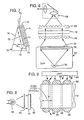
- the display subassembly 12 is positioned on the transparent projection surface 50 of a conventional overhead projector 52.
- a conventional overhead projector 52 typically include an illumination bulb 54 and a Fresnel lens 56 under the projection surface to produce light beams that pass through a transparency and converge onto a projection lens assembly 58.
- this lens is often formed by cementing two or more lower powered Fresnel lenses together.
- a Fresnel lens 60 as the entrance optic to collimate the converging light from the projection surface prior to illumination of the display subassembly.
- the light exiting the subassembly is then refocused by a exit optic lens 62 (which is also desirably in Fresnel form) onto the projection lens assembly 58.
- exit optic lens 62 which serves the same purpose as the Fresnel lens provided under the projection surface of the projector in the projector's normal operation, namely to focus light towards the projection lens assembly 58.
- a backlit viewing stand 70 shown in Fig. 7 may be employed.
- This stand has a light-transmitting surface 71 against which the display 12 can rest, and an internal light source 72 for directing illumination through the light-transmitting surface.
- a small shelf 73 on which the display can be positioned is provided on the exterior of the stand.
- the stand 70 is desirably collapsible to permit ready portability. This can be achieved with a hinge and bellows arrangement 74. A small size can be maintained by using folded optics that include mirroring on the inside back wall 76 of the stand.
- the stand 70 is also desirably provided with optics that emulate the optics of a conventional overhead projector. That is, these optics focus light incident on the display 12 so that it converges on a point a short distance away.
- these optics comprise a Fresnel plate lens 75.
- the Fresnel entrance optic 60 used with the display 12 in the Fig. 6 embodiment (present but not particularly shown in Fig. 7) again collimates this focused light prior to its illumination of the display subassembly.
- the exit optic 18 is a simple translucent dispersion medium, such as a ground glass plate or a commercially available diffusion material (i.e. Rolux film manufactured by Rosco of Port Chester N.Y.).
- the viewing stand 70 advantageously permits an LCD display to be used either as a projection device for large audiences (i.e. as an "electronic transparency"), or as a single-user computer screen. Such multiple functionality for an LCD display has not heretofore been available.
- a second application of the high resolution display subassembly 12 is as a dedicated backlit screen for a computer or the like.
- the subassembly 12 is illuminated with collimated light, and a translucent light dispersing material 80 is mounted adjacent the first polarizer 28 to display the resulting image.
- the collimated excitation light can be provided from a relatively low wattage bulb 82 in conjunction with a thin lens 84.
- a direct view display may be illuminated by a fluorescent light panel 90.
- the display subassembly 12 is fabricated with an entrance plate 92 on which are formed a plurality of microlenses 94, one aligned to each pixel of the display.
- Light incident on one of microlenses 94, regardless of its orientation, is directed normal to the plane of the display subassembly 12 and thus passes through the pixels of the component layers in the proper alignment.
- collimated light exiting the subassembly 12 is dispersed by microlenses 96 which permit the resultant image to be viewed from a wide range of angles without parallax effects.
- the interstitial areas 98 between the lenses may be colored black to minimize stray light and to improve perceived contrast.
- the exit optic can be a simple light dispersing medium, such as the ground glass plate 80 shown in Fig. 8.
- the incident light can be collimated by a novel arrangement employing a parabolic mirror 100 (desirably in Fresnel form) and a micro-venetian blind material 102.
- this embodiment is illuminated by a pair of linear light sources, such as fluorescent bulbs 104. These bulbs illuminate a generally flat mirrored surface 106 that has facets arranged to provide one axis of collimation. The angles of the facets vary with placement on the surface to simulate a sectioned parabolic reflector. Light reflected from this mirrored surface is substantially collimated.
- a micro-venetian blind material 102 such as Light Control Film marketed by 3M Corp, is desirably placed between the mirror and the display subassembly.
- This material is a thin plastic film containing closely spaced black microlouvers to absorb light misaligned with respect to the louvers.
- the present invention overcomes the electrical and interconnection constraints that have previously limited liquid crystal displays to relatively low resolution applications.
- one panel may have a plurality of contiguous rows that form the top portion of the display, and the second panel may have a plurality of contiguous rows that form the bottom portion of the display.
- the display subassembly has been described as providing a monochromatic display, it will be recognized that several such displays can be stacked and operated cooperatively to provide a full color display.
- one display (comprised of two or more stacked panels) can be tuned to switch between the colors cyan and white, a second display can be tuned to switch between magenta and white, and a third display can tuned to switch between yellow and white.
- These three displays, stacked with polarizers (which may be colored for increased transmissivity) can yield a high resolution full color display.
Abstract
Description
- This application is a continuation-in-part of copending application Serial No. 07/363,099, filed June 7, 1989, which in turn is a continuation-in-part of copending application Serial No. 07/329,938, filed March 28, 1989.
- The present invention relates to LCD display systems, and more particularly relates to display systems employing a plurality of LCD panels in series stacked arrangement to permit increased display resolution.
- LCD panels are finding increasing applicability in sophisticated display devices. A drawback to their further exploitation, however, is their relatively limited resolution.
- The resolution of LCD panels is limited both by interconnection constraints and by the electrical properties of the liquid crystal material itself. Taking this latter limitation first, in any multiplexed LCD display, each cell must be electrically refreshed periodically, typically 30 or 60 times a second, to maintain its desired state. This is effected by repetitively scanning down the panel, refreshing each row in turn. The greater the resolution of a panel, the greater the number of rows that must be refreshed at this rate. Beyond a certain limit, the period allotted to refreshing each row becomes too short to refresh it effectively. Thus, a minimum refresh period limits the number of rows that can be refreshed at the requisite rate. This number is about 250 - 300 rows with current liquid crystal materials.
- In the prior art, displays with twice this number of rows have been achieved by duplicating the refresh circuitry so that half the rows of the panel are refreshed by one circuit and half are refreshed by the other. Thus, at any instant, two rows are being refreshed -- one by one circuit and one by the other. However, this technique still only permits 500 or so rows of resolution. Truly high resolution applications demand substantially more rows.
- The obstacle to refreshing more than 500 rows is the interconnection limitation. The refresh circuitry must connect to each column of pixels on the display. There may be 640 or more such columns. By partitioning the display into top and bottom portions, the two requisite 640 wire connections can be made -- one along the top of the display and one along the bottom. However, this partitioning approach cannot be extended to a three-or more way division because there is no way to make the requisite interconnect to intermediate portions of the display.
- The interconnect limitation is generally accepted to be an absolute bar to arbitrarily-high resolution LCD displays, as noted in "Scanning Limitations of Liquid Crystal Displays" by P.M. Alt et al, IEEE Trans. Electron Devices, Vol. ED-21, pp. 146-155 (1974); and "Ultimate Limits for Matrix Addressing of RMS-Responding L.C.D.'s" by J. Nehring et al, IEEE Trans. Electron. Devices, Vol. ED-26, p. 795-802 (1979).
- It is a principal object of the present invention to provide a display that circumvents both the electrical and interconnect limitations, permitting fabrication of LCD displays of virtually unlimited resolution.
- In accordance with the present invention, a composite display is fabricated with a plurality of panels. Each panel has active rows and inactive rows. The panels are stacked and aligned so that each active row is in alignment with inactive rows in all the other panels of the stack. The parallax problem inherent with this stacked cell approach is eliminated by a lens system that collimates light illuminating the stacked assembly. The limited viewing angle associated with collimated illumination is overcome by an exit optic that may either focus or disperse the exiting light for viewing.
- The foregoing and additional objects, features and advantages of the present invention will be more readily apparent from the following detailed description thereof, which proceeds with reference to the accompanying drawings.
-
- Fig. 1 is a partial schematic side view of a high resolution display system according to one embodiment of the present invention.
- Fig. 2 is a partial top view of an LCD panel used in the display subassembly of Fig. 1.
- Fig. 3 is a partial top view of the subassembly of Fig. 1.
- Fig. 4 is a partial side view of a display subassembly using double cells that may be employed in the display system of Fig 1.
- Fig. 5 is a partial side view of a display subassembly using a different implementation of double cells that may be employed in the display system of Fig. 1.
- Fig. 6 is a view of a display system using a display subassembly according to the present invention in conjunction with a conventional overhead projector.
- Fig. 7 is a view of a display stand according to the present invention.
- Fig. 8 shows a direct view display system according to the present invention.
- Fig. 9 shows another direct view display system according to the present invention.
- Fig. 10 shows yet another direct view display system according to the present invention.
- Fig. 11 is a partial side view of a display subassembly in which the active rows are distributed over four panels.
- Referring to Fig. 1, a display system 10 according to one embodiment of the present invention includes a
display subassembly 12, anillumination source 14, an entrance optic 16, an exit optic 18, anddisplay driver circuitry 20. - The
display subassembly 12 includes first andsecond panels transparent electrodes 26 that can be controllably energized to change the state of the liquid crystal material sandwiched therebetween. In the illustrated panels, the electrodes are arranged inrows 17 that define active areas, interlaced withrows 19 without electrodes, which define inactive areas. The two panels are stacked and aligned so that the active rows of one panel are in optical alignment with the inactive rows of the other panel. By this arrangement, the composite subassembly provides twice the number of rows of either panel by itself, yet avoids the fabrication difficulties associated with putting all these active rows on a single panel. - In the illustrated embodiment, each of the
panels - Fig. 2 is a partial top view of the
first panel 22 showing the alternating active and inactive rows. Fig. 3 is a partial top view of thestacked subassembly 12 showing the interlacing of rows. - Sandwiching the two
LCD panels second polarizers third polarizer 32 is interposed between the panels. - The
display driver circuitry 20 includes asource 34 of display data, such as a computer or the like, and first andsecond driver circuits first driver circuit 36 operates to receive display data from thesource 34 and to provide data corresponding to the first, third, fifth video rows, etc, to driver circuitry that operates the active rows in thefirst panel 22. This driver circuitry is conventional and operates by partitioning the panel into top and bottom halves and refresh-scanning both halves simultaneously, as described in the Background of the Invention section. Thefirst driver circuit 36 ignores the data relating the second, fourth, etc. rows. Thesecond driver circuit 38 performs likewise with the second, fourth, sixth, etc. rows. - The
display driver circuitry 20 used in the illustrated embodiment is also conventional, being another application of the well known display drivers that control two scans simultaneously. - The Fig. 1 embodiment can be practiced with virtually any LCD construction, such as twisted nematic, supertwisted nematic, double supertwisted nematic, etc. Double supertwisted nematic is particularly desirable in high resolution displays because it can provide a virtually true black and white image, as opposed to the color tinted images produced by the other technologies. In double supertwisted nematic panel construction, an additional, passive liquid crystal cell is used in conjunction with the primary liquid crystal cell to compensate for optical wavelength dependence in the primary cell. The passive cell is essentially identical to the primary cell except it has an opposite twist sense.
- Fig. 4 shows a
display subassembly 12′ using double supertwisted panels. Thefirst panel 22′ includes anoperative panel 22a′ and apassive panel 22b′. Theoperative panel 22a′ includes electrodes 26'and is operated in conjunction with thepassive panel 22b′ that is fabricated without electrodes and with an opposite twist sense. Thesecond panel 24′ is constructed similarly. - The construction of the double supertwisted display subassembly of Fig. 4 can be simplified considerably by fabricating the first and second primary panels to have opposite twist senses. In such an embodiment, the inactive portions of one panel serve as the passive, reverse twist counterparts to the active portions of the other panel. Such an embodiment is shown in Fig. 5. In addition to eliminating two liquid crystal layers, this embodiment also permits the
intermediate polarizer 32′ to be omitted. - In order for these stacked panel display subassemblies to work without parallax limitations, the
entrance optic 16 desirably collimates the illumination from thelight source 14 in a direction orthogonal to the panels. Thisentrance optic 16 can take many forms, as discussed below. The collimated light exiting the display subassembly is also typically processed by anexit optic 18 which can either focus the light for projection on a viewing surface, or can simply disperse the light for direct viewing. - Referring to Fig. 6, in a first application the
display subassembly 12 is positioned on thetransparent projection surface 50 of a conventionaloverhead projector 52. Such projectors typically include anillumination bulb 54 and aFresnel lens 56 under the projection surface to produce light beams that pass through a transparency and converge onto aprojection lens assembly 58. (Due to the short focal length and high power required oflens 56, this lens is often formed by cementing two or more lower powered Fresnel lenses together.) - When
display subassembly 12 is used in the Fig. 6 application, it is desirable to provide aFresnel lens 60 as the entrance optic to collimate the converging light from the projection surface prior to illumination of the display subassembly. The light exiting the subassembly is then refocused by a exit optic lens 62 (which is also desirably in Fresnel form) onto theprojection lens assembly 58. (Lens 62 here serves the same purpose as the Fresnel lens provided under the projection surface of the projector in the projector's normal operation, namely to focus light towards theprojection lens assembly 58.) - If it is desired to use the Fig. 6 display system in a direct view arrangement, a backlit viewing stand 70 shown in Fig. 7 may be employed. This stand has a light-transmitting
surface 71 against which thedisplay 12 can rest, and an internallight source 72 for directing illumination through the light-transmitting surface. Asmall shelf 73 on which the display can be positioned is provided on the exterior of the stand. - The stand 70 is desirably collapsible to permit ready portability. This can be achieved with a hinge and bellows
arrangement 74. A small size can be maintained by using folded optics that include mirroring on theinside back wall 76 of the stand. - The stand 70 is also desirably provided with optics that emulate the optics of a conventional overhead projector. That is, these optics focus light incident on the
display 12 so that it converges on a point a short distance away. In the illustrated embodiment, these optics comprise aFresnel plate lens 75. TheFresnel entrance optic 60 used with thedisplay 12 in the Fig. 6 embodiment (present but not particularly shown in Fig. 7) again collimates this focused light prior to its illumination of the display subassembly. - In this application, the
exit optic 18 is a simple translucent dispersion medium, such as a ground glass plate or a commercially available diffusion material (i.e. Rolux film manufactured by Rosco of Port Chester N.Y.). - It will be recognized that the viewing stand 70 advantageously permits an LCD display to be used either as a projection device for large audiences (i.e. as an "electronic transparency"), or as a single-user computer screen. Such multiple functionality for an LCD display has not heretofore been available.
- A second application of the high
resolution display subassembly 12 is as a dedicated backlit screen for a computer or the like. In this application, shown in Fig. 8, thesubassembly 12 is illuminated with collimated light, and a translucentlight dispersing material 80 is mounted adjacent thefirst polarizer 28 to display the resulting image. The collimated excitation light can be provided from a relativelylow wattage bulb 82 in conjunction with athin lens 84. - In a related embodiment shown in Fig. 9, a direct view display may be illuminated by a fluorescent
light panel 90. In such embodiments thedisplay subassembly 12 is fabricated with anentrance plate 92 on which are formed a plurality ofmicrolenses 94, one aligned to each pixel of the display. Light incident on one ofmicrolenses 94, regardless of its orientation, is directed normal to the plane of thedisplay subassembly 12 and thus passes through the pixels of the component layers in the proper alignment. - The same arrangement may be used on the exiting side of the display. In this case, collimated light exiting the
subassembly 12 is dispersed bymicrolenses 96 which permit the resultant image to be viewed from a wide range of angles without parallax effects. Theinterstitial areas 98 between the lenses may be colored black to minimize stray light and to improve perceived contrast. Alternatively, the exit optic can be a simple light dispersing medium, such as theground glass plate 80 shown in Fig. 8. - In still a further variation of the direct view embodiment, the incident light can be collimated by a novel arrangement employing a parabolic mirror 100 (desirably in Fresnel form) and a micro-venetian
blind material 102. As shown in Fig. 10, this embodiment is illuminated by a pair of linear light sources, such asfluorescent bulbs 104. These bulbs illuminate a generally flat mirroredsurface 106 that has facets arranged to provide one axis of collimation. The angles of the facets vary with placement on the surface to simulate a sectioned parabolic reflector. Light reflected from this mirrored surface is substantially collimated. However, to remove any stray off-axis light, a micro-venetianblind material 102, such as Light Control Film marketed by 3M Corp, is desirably placed between the mirror and the display subassembly. This material is a thin plastic film containing closely spaced black microlouvers to absorb light misaligned with respect to the louvers. By this arrangement, a very compact and efficient display can be provided. - From the foregoing description, it will be recognized that the present invention overcomes the electrical and interconnection constraints that have previously limited liquid crystal displays to relatively low resolution applications.
- Having described and illustrated the principles of our invention with reference to a preferred embodiment and several variations thereon, it should be apparent that the invention can be modified in arrangement and detail without departing from such principles. For example, while the display subassembly has been described as having its active rows distributed between two stacked panels, it will be recognized that in alternative embodiments the active rows may be distributed among three or more panels to attain still higher resolution. Such an arrangement, employing active rows on four panels, is shown in Fig. 11. Similarly, while the display subassembly has been described as having active rows on one panel interlaced with active rows on another panel, it will be recognized that the rows need not be interlaced. Instead, for example, one panel may have a plurality of contiguous rows that form the top portion of the display, and the second panel may have a plurality of contiguous rows that form the bottom portion of the display. Finally, while the display subassembly has been described as providing a monochromatic display, it will be recognized that several such displays can be stacked and operated cooperatively to provide a full color display. In one such embodiment, one display (comprised of two or more stacked panels) can be tuned to switch between the colors cyan and white, a second display can be tuned to switch between magenta and white, and a third display can tuned to switch between yellow and white. These three displays, stacked with polarizers (which may be colored for increased transmissivity) can yield a high resolution full color display.
- In view of these and the wide variety of other embodiments to which the principles of our invention may be applied, it should be recognized that the illustrated embodiments are to be considered illustrative only and not as limiting the scope of the invention. Instead, we claim as our invention all such modifications as may come within the scope and spirit of the following claims and equivalents thereto.
- The features disclosed in the foregoing description, in the claims and/or in the accompanying drawings may, both separately and in any combination thereof, be material for realising the invention in diverse forms thereof.
Claims (11)
first and second polarizers; and
first and second LCD panels stacked between the first and second polarizers, each of said panels having a plurality of active rows and a plurality of inactive rows, each of the active rows being comprised of a plurality of pixels, the two panels being aligned with each other so that each active row in one panel is in optical alignment with an inactive row in the other panel, wherein the two panels can be cooperatively operated to yield a composite display whose resolution includes all of the active rows in the first panel plus all the active rows in the second panel.
means for collimating light entering the display subassembly in a direction orthogonal thereto.
means for receiving light focused on a predetermined point and for collimating said light for illumination of the display subassembly; and
means for re-focusing the collimated light exiting the display subassembly back onto the predetermined point;
wherein the display system can be utilized on the display surface of a conventional overhead projector.
Applications Claiming Priority (2)
| Application Number | Priority Date | Filing Date | Title |
|---|---|---|---|
| US378997 | 1989-07-12 | ||
| US07/378,997 US4952036A (en) | 1989-06-07 | 1989-07-12 | High resolution LCD display system |
Publications (2)
| Publication Number | Publication Date |
|---|---|
| EP0408036A2 true EP0408036A2 (en) | 1991-01-16 |
| EP0408036A3 EP0408036A3 (en) | 1992-05-13 |
Family
ID=23495392
Family Applications (1)
| Application Number | Title | Priority Date | Filing Date |
|---|---|---|---|
| EP19900113374 Ceased EP0408036A3 (en) | 1989-07-12 | 1990-07-12 | High resolution lcd display system |
Country Status (5)
| Country | Link |
|---|---|
| US (1) | US4952036A (en) |
| EP (1) | EP0408036A3 (en) |
| JP (1) | JPH0346627A (en) |
| AU (1) | AU629662B2 (en) |
| CA (1) | CA2021071A1 (en) |
Cited By (3)
| Publication number | Priority date | Publication date | Assignee | Title |
|---|---|---|---|---|
| EP0523987A1 (en) * | 1991-07-15 | 1993-01-20 | Sharp Kabushiki Kaisha | Liquid crystal display system |
| WO2004053586A1 (en) * | 2002-12-11 | 2004-06-24 | Optiva, Inc. | Liquid crystal shutter |
| EP1434082A1 (en) * | 2000-01-11 | 2004-06-30 | Kabushiki Kaisha Toshiba | Multidomain liquid crystal display device with two liquid crystal layers |
Families Citing this family (41)
| Publication number | Priority date | Publication date | Assignee | Title |
|---|---|---|---|---|
| US5299039A (en) * | 1988-07-21 | 1994-03-29 | Proxima Corporation | Stacked display panel construction and method of aligning pixel elements thereof |
| US5272553A (en) * | 1988-10-28 | 1993-12-21 | Sharp Kabushiki Kaisha | Projection type liquid crystal display device with twisted nematic liquid crystal layers |
| US5235446A (en) * | 1989-02-09 | 1993-08-10 | Sharp Kabushiki Kaisha | Projection type liquid crystal display apparatus with pixels of one panel |
| US5124818A (en) * | 1989-06-07 | 1992-06-23 | In Focus Systems, Inc. | LCD system having improved contrast ratio |
| IL92555A0 (en) * | 1989-12-05 | 1990-08-31 | Michael Stalow | Multilayer parallax-free liquid crystal device |
| IL92936A (en) | 1989-12-31 | 1998-02-08 | Smartlight Ltd | Self-masking transparency viewing apparatus |
| US6311419B1 (en) | 1989-12-31 | 2001-11-06 | Smartlight Ltd. | Dedicated mammogram viewer |
| US5268782A (en) * | 1992-01-16 | 1993-12-07 | Minnesota Mining And Manufacturing Company | Micro-ridged, polymeric liquid crystal display substrate and display device |
| US5365356A (en) * | 1992-08-11 | 1994-11-15 | Minnesota Mining And Manufacturing Company | Method of fabricating an encapsulated liquid crystal display |
| JPH08509555A (en) * | 1993-02-03 | 1996-10-08 | プレーン,ホルスト | Image modulation method and device for displaying optical effect |
| US5439621A (en) * | 1993-04-12 | 1995-08-08 | Minnesota Mining And Manufacturing Company | Method of making an array of variable focal length microlenses |
| US5481651A (en) * | 1993-04-26 | 1996-01-02 | Motorola, Inc. | Method and apparatus for minimizing mean calculation rate for an active addressed display |
| AU6702294A (en) * | 1993-05-10 | 1994-12-12 | Motorola, Inc. | Method and apparatus for receiving and processing compressed image data for presentation by an active-addressed display |
| GB9310190D0 (en) * | 1993-05-18 | 1993-06-30 | Negretti Aviat Ltd | Display system |
| EP0700547A1 (en) * | 1993-05-24 | 1996-03-13 | Motorola, Inc. | Method and apparatus for storing compressed data for subsequent presentation on an active addressed display |
| CN1104004A (en) * | 1993-05-24 | 1995-06-21 | 莫托罗拉公司 | Method and apparatus for processing and subsequently displaying transmitted image data on an active-addressed display device |
| US5598179A (en) * | 1993-06-14 | 1997-01-28 | Motorola, Inc. | Method and apparatus for driving electronic displays |
| US5459482A (en) * | 1993-06-24 | 1995-10-17 | Motorola, Inc. | Facsimile communication with an active addressing display device |
| US5475397A (en) * | 1993-07-12 | 1995-12-12 | Motorola, Inc. | Method and apparatus for reducing discontinuities in an active addressing display system |
| SE9402666L (en) * | 1993-08-09 | 1995-02-10 | Motorola Inc | Methods and apparatus for reducing memory requirements in a presentation system with active addressing and reduced line addressing |
| US5457551A (en) * | 1993-10-08 | 1995-10-10 | Planar Systems, Inc. | Frame response compensated, video rate addressable liquid crystal passive matrix display system |
| EP0918241A3 (en) * | 1993-11-28 | 1999-06-23 | Smartlight Limited | Transparency viewing device |
| DE4409087A1 (en) * | 1994-03-17 | 1995-09-21 | Blaupunkt Werke Gmbh | Display device |
| US5719650A (en) * | 1995-05-12 | 1998-02-17 | Massachusetts Institute Of Technology | High-fidelity spatial light modulator |
| US5801800A (en) * | 1996-04-29 | 1998-09-01 | Motorola, Inc. | Visual display system for display resolution enhancement |
| SE509638C2 (en) * | 1996-06-15 | 1999-02-15 | Allgon Ab | Meander antenna device |
| US5963276A (en) * | 1997-01-09 | 1999-10-05 | Smartlight Ltd. | Back projection transparency viewer with overlapping pixels |
| JP2008524665A (en) * | 2004-12-21 | 2008-07-10 | コーニンクレッカ フィリップス エレクトロニクス エヌ ヴィ | Display device for visually reconstructing images |
| JP5176194B2 (en) * | 2006-04-18 | 2013-04-03 | Nltテクノロジー株式会社 | Liquid crystal display device and image display system |
| US7821474B2 (en) * | 2006-10-13 | 2010-10-26 | Apple Inc. | Rendering luminance levels of a high dynamic range display |
| JPWO2010100807A1 (en) * | 2009-03-02 | 2012-09-06 | 九州ナノテック光学株式会社 | Liquid crystal blind device and its use |
| JP5417005B2 (en) * | 2009-03-26 | 2014-02-12 | パナソニック株式会社 | Lighting device |
| US9135864B2 (en) | 2010-05-14 | 2015-09-15 | Dolby Laboratories Licensing Corporation | Systems and methods for accurately representing high contrast imagery on high dynamic range display systems |
| CN102466919B (en) * | 2010-10-29 | 2014-11-05 | 京东方科技集团股份有限公司 | Color film substrate, manufacture method thereof, and three-dimensional (3D) liquid crystal display (LCD) provided therewith |
| JP5914530B2 (en) | 2011-03-09 | 2016-05-11 | ドルビー ラボラトリーズ ライセンシング コーポレイション | High contrast grayscale and color display |
| TW201324468A (en) * | 2011-12-12 | 2013-06-16 | Wintek Corp | Touch display device |
| US10134295B2 (en) | 2013-09-20 | 2018-11-20 | Bose Corporation | Audio demonstration kit |
| US9984583B2 (en) | 2013-09-20 | 2018-05-29 | Bose Corporation | Audio demonstration kit |
| EP3086167A4 (en) * | 2013-12-19 | 2017-09-13 | Citizen Watch Co., Ltd. | Optical modulation element |
| CN108885377B (en) | 2018-06-14 | 2021-12-24 | 京东方科技集团股份有限公司 | Display device and driving method thereof |
| US10923079B2 (en) * | 2019-04-04 | 2021-02-16 | Hisense Visual Technology Co., Ltd. | Dual-cell display apparatus |
Citations (7)
| Publication number | Priority date | Publication date | Assignee | Title |
|---|---|---|---|---|
| DE2844572A1 (en) * | 1977-10-14 | 1979-04-26 | Sharp Kk | MULTI-LAYER LIQUID CRYSTAL DISPLAY IN A MATRIX ARRANGEMENT |
| JPS5484999A (en) * | 1978-10-06 | 1979-07-06 | Sharp Corp | Matrix-type liquid crystal display device |
| GB2066498A (en) * | 1979-12-20 | 1981-07-08 | Sharp Kk | Multi-layered Twisted Nematic Liquid Crystal Display Panel |
| JPS6146930A (en) * | 1984-08-10 | 1986-03-07 | Ricoh Co Ltd | Liquid crystal display method and its display device |
| EP0259058A2 (en) * | 1986-08-20 | 1988-03-09 | Fujitsu Limited | Projection-type multi-colour liquid crystal display device |
| EP0284372A2 (en) * | 1987-03-23 | 1988-09-28 | Sharp Kabushiki Kaisha | A liquid-crystal display device |
| EP0366499A2 (en) * | 1988-10-28 | 1990-05-02 | Sharp Kabushiki Kaisha | Liquid crystal display device |
Family Cites Families (8)
| Publication number | Priority date | Publication date | Assignee | Title |
|---|---|---|---|---|
| JPS609767Y2 (en) * | 1979-07-31 | 1985-04-05 | シャープ株式会社 | electrochromic display device |
| JPS5685780A (en) * | 1979-12-14 | 1981-07-13 | Casio Computer Co Ltd | Liquid crystal display unit |
| JPS56150785A (en) * | 1980-04-23 | 1981-11-21 | Hitachi Ltd | Liquid crystal display unit |
| US4641923A (en) * | 1980-07-03 | 1987-02-10 | Control Interface Company Limited | Field sensitive optical displays with electrodes with high and low impedance portions |
| JP2516922B2 (en) * | 1986-07-04 | 1996-07-24 | 株式会社日立製作所 | Liquid crystal display |
| JPS6344624A (en) * | 1986-08-12 | 1988-02-25 | Fuji Photo Film Co Ltd | Liquid crystal device |
| US4810058A (en) * | 1986-10-24 | 1989-03-07 | Brother Kogyo Kabushiki Kaisha | Exposure device utilizing a liquid crystal shutter matrix |
| US4798448A (en) * | 1988-02-16 | 1989-01-17 | General Electric Company | High efficiency illumination system for display devices |
-
1989
- 1989-07-12 US US07/378,997 patent/US4952036A/en not_active Expired - Fee Related
-
1990
- 1990-07-12 CA CA002021071A patent/CA2021071A1/en not_active Abandoned
- 1990-07-12 AU AU58970/90A patent/AU629662B2/en not_active Expired
- 1990-07-12 EP EP19900113374 patent/EP0408036A3/en not_active Ceased
- 1990-07-12 JP JP2182873A patent/JPH0346627A/en active Pending
Patent Citations (7)
| Publication number | Priority date | Publication date | Assignee | Title |
|---|---|---|---|---|
| DE2844572A1 (en) * | 1977-10-14 | 1979-04-26 | Sharp Kk | MULTI-LAYER LIQUID CRYSTAL DISPLAY IN A MATRIX ARRANGEMENT |
| JPS5484999A (en) * | 1978-10-06 | 1979-07-06 | Sharp Corp | Matrix-type liquid crystal display device |
| GB2066498A (en) * | 1979-12-20 | 1981-07-08 | Sharp Kk | Multi-layered Twisted Nematic Liquid Crystal Display Panel |
| JPS6146930A (en) * | 1984-08-10 | 1986-03-07 | Ricoh Co Ltd | Liquid crystal display method and its display device |
| EP0259058A2 (en) * | 1986-08-20 | 1988-03-09 | Fujitsu Limited | Projection-type multi-colour liquid crystal display device |
| EP0284372A2 (en) * | 1987-03-23 | 1988-09-28 | Sharp Kabushiki Kaisha | A liquid-crystal display device |
| EP0366499A2 (en) * | 1988-10-28 | 1990-05-02 | Sharp Kabushiki Kaisha | Liquid crystal display device |
Non-Patent Citations (2)
| Title |
|---|
| PATENT ABSTRACTS OF JAPAN, vol. 10, no. 206 (P-478)(2262), 18th July 1986; & JP-A-61 046 930 (RICOH) 07-03-1986 * |
| PATENT ABSTRACTS OF JAPAN, vol. 3, no. 107 (E-136), 8th September 1979; & JP-A-54 084 999 (SHARP K.K.) 07-06-1979 * |
Cited By (6)
| Publication number | Priority date | Publication date | Assignee | Title |
|---|---|---|---|---|
| EP0523987A1 (en) * | 1991-07-15 | 1993-01-20 | Sharp Kabushiki Kaisha | Liquid crystal display system |
| US5329388A (en) * | 1991-07-15 | 1994-07-12 | Sharp Kabushiki Kaisha | Liquid crystal display employing light guide plate between cells |
| EP1434082A1 (en) * | 2000-01-11 | 2004-06-30 | Kabushiki Kaisha Toshiba | Multidomain liquid crystal display device with two liquid crystal layers |
| US6987550B2 (en) | 2000-01-11 | 2006-01-17 | Kabushiki Kaisha Toshiba | Liquid crystal display device |
| US6989880B2 (en) | 2000-01-11 | 2006-01-24 | Kabushiki Kaisha Toshiba | Liquid crystal display device |
| WO2004053586A1 (en) * | 2002-12-11 | 2004-06-24 | Optiva, Inc. | Liquid crystal shutter |
Also Published As
| Publication number | Publication date |
|---|---|
| US4952036A (en) | 1990-08-28 |
| EP0408036A3 (en) | 1992-05-13 |
| JPH0346627A (en) | 1991-02-27 |
| CA2021071A1 (en) | 1991-01-13 |
| AU5897090A (en) | 1991-01-17 |
| AU629662B2 (en) | 1992-10-08 |
Similar Documents
| Publication | Publication Date | Title |
|---|---|---|
| US4952036A (en) | High resolution LCD display system | |
| US5161041A (en) | Lighting assembly for a backlit electronic display including an integral image splitting and collimating means | |
| US5231432A (en) | Projector utilizing liquid crystal light-valve and color selection by diffraction | |
| US5608551A (en) | Display panel assembly with microlens structure | |
| US5594561A (en) | Flat panel display with elliptical diffuser and fiber optic plate | |
| US4915479A (en) | Liquid crystal display illumination system | |
| US4257041A (en) | Electro optical display device | |
| US6864861B2 (en) | Image generator having a miniature display device | |
| US11294173B2 (en) | Display device and head-up display device | |
| US5108172A (en) | Active matrix reflective image plane module and projection system | |
| US5022750A (en) | Active matrix reflective projection system | |
| US4976536A (en) | Liquid crystal display for projection systems | |
| TW321759B (en) | ||
| US20050073625A1 (en) | Surface light source and liquid crystal display device using the same | |
| EP0598608A1 (en) | Direct-view display apparatus | |
| US6700557B1 (en) | Electrode border for spatial light modulating displays | |
| KR920001415A (en) | Color liquid crystal display device | |
| WO1994016354A1 (en) | Color liquid crystal display system | |
| EP0645661A1 (en) | Liquid crystal projection panel | |
| KR19990077317A (en) | Color separation backlight | |
| JP2810572B2 (en) | Projection display device | |
| US7061678B1 (en) | Stereoscopic display device with two back light sources | |
| WO1995024671A1 (en) | Electromagnetic beam scanning arrays and electro-optical image display systems incorporating the same | |
| US20210072451A1 (en) | Switchable illumination apparatus and privacy display | |
| US5777706A (en) | Nematic liquid crystal phase spatial light modulator for enhanced display resolution |
Legal Events
| Date | Code | Title | Description |
|---|---|---|---|
| PUAI | Public reference made under article 153(3) epc to a published international application that has entered the european phase |
Free format text: ORIGINAL CODE: 0009012 |
|
| AK | Designated contracting states |
Kind code of ref document: A2 Designated state(s): AT BE CH DE DK ES FR GB GR IT LI LU NL SE |
|
| PUAL | Search report despatched |
Free format text: ORIGINAL CODE: 0009013 |
|
| AK | Designated contracting states |
Kind code of ref document: A3 Designated state(s): AT BE CH DE DK ES FR GB GR IT LI LU NL SE |
|
| 17P | Request for examination filed |
Effective date: 19921112 |
|
| 17Q | First examination report despatched |
Effective date: 19940627 |
|
| STAA | Information on the status of an ep patent application or granted ep patent |
Free format text: STATUS: THE APPLICATION HAS BEEN REFUSED |
|
| 18R | Application refused |
Effective date: 19951113 |