EP0410679B1 - Method for preparing a substrate for forming semiconductor devices - Google Patents
Method for preparing a substrate for forming semiconductor devices Download PDFInfo
- Publication number
- EP0410679B1 EP0410679B1 EP90308060A EP90308060A EP0410679B1 EP 0410679 B1 EP0410679 B1 EP 0410679B1 EP 90308060 A EP90308060 A EP 90308060A EP 90308060 A EP90308060 A EP 90308060A EP 0410679 B1 EP0410679 B1 EP 0410679B1
- Authority
- EP
- European Patent Office
- Prior art keywords
- wafer
- wafers
- warp
- oxide film
- bonded
- Prior art date
- Legal status (The legal status is an assumption and is not a legal conclusion. Google has not performed a legal analysis and makes no representation as to the accuracy of the status listed.)
- Expired - Lifetime
Links
- 239000000758 substrate Substances 0.000 title claims description 30
- 238000000034 method Methods 0.000 title claims description 25
- 239000004065 semiconductor Substances 0.000 title claims description 23
- 235000012431 wafers Nutrition 0.000 claims description 152
- XUIMIQQOPSSXEZ-UHFFFAOYSA-N Silicon Chemical compound [Si] XUIMIQQOPSSXEZ-UHFFFAOYSA-N 0.000 claims description 15
- 229910052710 silicon Inorganic materials 0.000 claims description 15
- 239000010703 silicon Substances 0.000 claims description 15
- 239000010409 thin film Substances 0.000 claims description 14
- 239000013078 crystal Substances 0.000 claims description 8
- 239000010408 film Substances 0.000 description 52
- 230000015572 biosynthetic process Effects 0.000 description 13
- 238000000227 grinding Methods 0.000 description 8
- 238000005530 etching Methods 0.000 description 7
- 239000012670 alkaline solution Substances 0.000 description 6
- 238000004519 manufacturing process Methods 0.000 description 5
- IJGRMHOSHXDMSA-UHFFFAOYSA-N Atomic nitrogen Chemical compound N#N IJGRMHOSHXDMSA-UHFFFAOYSA-N 0.000 description 4
- 238000005498 polishing Methods 0.000 description 4
- 230000000694 effects Effects 0.000 description 3
- 238000007796 conventional method Methods 0.000 description 2
- 238000002474 experimental method Methods 0.000 description 2
- 229910052757 nitrogen Inorganic materials 0.000 description 2
- 238000007254 oxidation reaction Methods 0.000 description 2
- 230000000295 complement effect Effects 0.000 description 1
- 238000002425 crystallisation Methods 0.000 description 1
- 230000008025 crystallization Effects 0.000 description 1
- 239000012212 insulator Substances 0.000 description 1
- 238000002955 isolation Methods 0.000 description 1
- 229910044991 metal oxide Inorganic materials 0.000 description 1
- 150000004706 metal oxides Chemical class 0.000 description 1
- 230000003647 oxidation Effects 0.000 description 1
- 238000000206 photolithography Methods 0.000 description 1
- 229910052594 sapphire Inorganic materials 0.000 description 1
- 239000010980 sapphire Substances 0.000 description 1
- 230000003746 surface roughness Effects 0.000 description 1
- 238000005979 thermal decomposition reaction Methods 0.000 description 1
- 230000009466 transformation Effects 0.000 description 1
- 239000012808 vapor phase Substances 0.000 description 1
Images


Classifications
-
- H—ELECTRICITY
- H01—ELECTRIC ELEMENTS
- H01L—SEMICONDUCTOR DEVICES NOT COVERED BY CLASS H10
- H01L21/00—Processes or apparatus adapted for the manufacture or treatment of semiconductor or solid state devices or of parts thereof
- H01L21/02—Manufacture or treatment of semiconductor devices or of parts thereof
- H01L21/04—Manufacture or treatment of semiconductor devices or of parts thereof the devices having at least one potential-jump barrier or surface barrier, e.g. PN junction, depletion layer or carrier concentration layer
- H01L21/18—Manufacture or treatment of semiconductor devices or of parts thereof the devices having at least one potential-jump barrier or surface barrier, e.g. PN junction, depletion layer or carrier concentration layer the devices having semiconductor bodies comprising elements of Group IV of the Periodic System or AIIIBV compounds with or without impurities, e.g. doping materials
- H01L21/20—Deposition of semiconductor materials on a substrate, e.g. epitaxial growth solid phase epitaxy
- H01L21/2003—Deposition of semiconductor materials on a substrate, e.g. epitaxial growth solid phase epitaxy characterised by the substrate
- H01L21/2007—Bonding of semiconductor wafers to insulating substrates or to semiconducting substrates using an intermediate insulating layer
-
- Y—GENERAL TAGGING OF NEW TECHNOLOGICAL DEVELOPMENTS; GENERAL TAGGING OF CROSS-SECTIONAL TECHNOLOGIES SPANNING OVER SEVERAL SECTIONS OF THE IPC; TECHNICAL SUBJECTS COVERED BY FORMER USPC CROSS-REFERENCE ART COLLECTIONS [XRACs] AND DIGESTS
- Y10—TECHNICAL SUBJECTS COVERED BY FORMER USPC
- Y10S—TECHNICAL SUBJECTS COVERED BY FORMER USPC CROSS-REFERENCE ART COLLECTIONS [XRACs] AND DIGESTS
- Y10S148/00—Metal treatment
- Y10S148/012—Bonding, e.g. electrostatic for strain gauges
Definitions
- This invention relates to an improved method for providing a substrate remarkably less in warp which is prepared for forming semiconductor devices and has an SOI (silicon on insulators) structure by means of bonding method.
- CMOS Complementary Metal-Oxide Semiconductors
- an oxide film (insulating layer) is formed on a silicon substrate, further a polycrystalline layer is precipitated on the oxide film, and then further a single crystalline thin film is formed through transformation of the polycrystalline layer by a laser beam irradiated thereonto.
- a method has been adopted in which a silicon polycrystalline thin film is formed on a sapphire substrate from vapor phase by way of thermal decomposition reaction for subsequent crystallization thereof.
- Fig. 4 (C) an example of the substrate in SOI structure for forming semiconductor devices is shown.
- Wafers 1a and 1b are bonded to each other with oxide films 1c interposed therebetween. Subsequently, the side exposed to the air of the wafer 1b is polished and/or etched to be a thin film so that this substrate is achieved.
- the preparing process will be more particularly described as follows:
- Fig. 4 (A) the wafers 1a and 1b both with high precision in flatness of the surfaces are thermally oxidized over the entire surface thereof to form an oxide film 1c 0.8 micrometer in thickness. Then, wafers 1a and 1b are superposed on each other (Fig. 4 (B)), then are put into a furnace in the state of superposition and further an electrical voltage of approximately 300 volts is applied in a pulse mode across the superposed wafers in an atmosphere of nitrogen at a temperature of about 500 degrees centigrade. In this way, wafers 1a and 1b are bonded to each other. The bonded wafers thus treated have a strong bonding strength therebetween so that the wafers can be put in the conventional IC manufacturing process as they stand.
- Wafer 1b of the bonded wafers thus obtained is polished and/or etched etc. from outside as it stands to be made into a thin film.
- a substrate with an SOI structure for forming semiconductor devices is prepared as shown in Fig. 4 (C).
- the above-mentioned wafers 1a and 1b have been requested to be polished like a mirror surface to have a high precision flatness, especially, on each surface to be bonded. Accordingly the surface has been finished so that the surface may have a highly precise flatness of 50 nm expressed in surface roughness.
- the bonded wafers will ordinarily have a warp convex at the outer surface of the wafer 1b.
- the warp will often be as large as several hundred micrometers. It is hard for the bonded wafers to be properly fixed by vacuum suction in this case. This causes a trouble in transcribing a mask pattern to the substrate in a photolithography exposure process wherein surface accuracy is highly required.
- wafers 1a and 1b had an oxide film 1c one micrometer thick formed on the entire surface by thermal oxidization, respectively.
- the wafers 1a and 1b were superposed on each other to be put into a furnace.
- the wafers had a pulse mode voltage of 350 volts applied at a temperature of 400 degrees centigrade for the purpose of bonding the wafers.
- the oxide film 1c covering the wafer 1b was removed and the bulk of the wafer was thinned by surface-grinding. Further, the wafer 1b was subjected to etching in an alkaline solution and to polishing so that the wafer 1b had a predetermined thickness.
- the warps were measured on one of the starting wafer and on the wafer or a bonded wafer after each of the following steps: Wafer 1a; wafer 1a which has had an oxide film 1c formed thereon; bonded wafers in which 1a and 1b have been bonded to each other; the bonded wafers which have been surface-ground; the bonded wafers which have been subjected to etching in an alkaline solution; and the bonded wafers which have been subjected to polishing.
- mark ( ⁇ ) is for the warp of the wafer 1a; mark ( ⁇ ) is for the warp of wafer 1a which has an oxide film formed thereon; mark ( ⁇ ) is for the warp of the bonded wafers; mark ( ⁇ ) is for the warp of bonded wafers which have been surface-ground; mark ( ⁇ ) is for the warp of the bonded wafers which have been subjected to etching in an alkaline solution; mark ( ⁇ ) is for the warp of the bonded wafers which have been subjected to polishing.
- Fig. 5 shows that the warp of the wafers which have been bonded is formed in the convex direction at the wafer 1b outside surface.
- Fig. 5 shows that there occurs a large deformation from the state of warp after bonding of the wafers ( ⁇ ) to the state of warp after surface grinding of wafer 1b ( ⁇ ).
- the front side i.e., the wafer 1b side was easy to turn convex in both of the above cases. It was also found that a warp always occurred regardless of the processes of thinning the wafer 1b into a thin film.
- an oxide film was formed on one side of an ordinary wafer to examine a warp of the wafer before and after the formation of an oxide film.
- An oxide film is different from silicon single crystal in thermal expansion coefficient. Silicon single crystal is greater in thermal expansion coefficient than an oxide film. Consequently, when an oxide film in formed on the entire surface of the silicon single crystal in a high temperature atmosphere and then cooled, residual stress is accumulated within the silicon single crystal. It is considered that when an oxide film is removed from the outside front (1b side) surface of the bonded wafers to make the wafer 1b thinner for the purpose of preparing an SOI structure, the residual stress on the wafer 1a causes the front or upper side of the bonded wafers to be warped upward (in this case, the extreme thinness to five micrometers or less of the wafer 1b allows the residual stress therein to be ignored).
- the influence of the oxide film 1c on the formation of warp can also be considered.
- the oxide film 1c between the individual wafers 1a and 1b is far thicker than the oxide film on the backside of the wafers. Therefore the oxide film 1c between the individual wafers 1a and 1b is far greater in influence on the formation of warp.
- This invention was made in the light of the above problems.
- the present invention comprises a method of preparing a substrate for forming semiconductor devices having an SOI structure wherein a first wafer and a second wafer each constituted by a silicon single crystal are bonded to each other with an oxide film interposed therebetween, polished and/or etched so that said second wafer is thinned into a thin film to prepare said substrate for forming semiconductor devices having an SOI structure, the improvement comprising steps of intentionally warping at least said first wafer prior to the bonding said second wafer to a concave side of said first wafer.
- the front or upper surface side of the substrate is subjected to deformation in the direction of the upper side in forming an SOI structure.
- the first wafer has a deformation formed in the reverse or downward direction in advance so that the substrate can be flat in result, when the SOI structure is formed.
- the first wafer is warped in advance. Then the second wafer is bonded to the concave side of the first wafer. A deformation of the bonded wafers at the time of forming an SOI structure reversed the warp of the bonded wafers to be offset, resulting in realization of a substrate for forming semiconductor devices having an SOI structure with an exceedingly flat surface.
- Figs. 1 (A) through (C) are views showing manufacturing processes in the preferred embodiments wherein a substrate for forming semiconductor devices having an SOI structure according to the present invention is prepared.
- Fig. 2 is a figure showing the relationship between the thickness of an oxide film and the warp.
- Fig. 3 is a figure showing the relationship between the thickness of the wafers and the warp.
- Figs. 4 (A) through (C) are views showing the manufacturing processes of a conventional method.
- Fig. 5 is a figure showing a warp at each process.
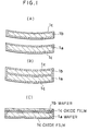
- Fig. 1 (C) shows a longitudinal sectional view of the substrate having an SOI structure.
- This substrate is manufactured from a pair of bonded wafers in which the wafer 1a and wafer 1b are bonded to each other with an oxide film 1c interposed therebetween, the wafer 1b being polished and/or etched into a thin film.
- wafers 1a and 1b are warped beforehand.
- Wafer 1b is bonded to the concave side of wafer 1a.
- Wafer 1b to be bonded may be completely free from warp.
- wafer 1b preferably has a warp formed in the same direction as 1a.
- the magnitude of the warp of wafer 1a at the time of bonding depends upon the diameters and the thicknesses of the wafers and also upon the temperature for forming the oxide film and the thicknesses thereof.
- the degrees of the warp can be determined as follows:
- Fig. 2 shows the relationship between the thickness of the oxide film and warp.
- a warp is shown for p-type wafers which are 150 mm in diameter and 625 micrometers in thickness.
- the wafers have the one side thereof formed with an oxide film 1,000 nm and 500 nm thick, respectively.
- On the axis of abscissa the warp of wafers prior to formation of the oxide films is shown.
- the conditions of forming the oxide films are the same.
- Fig. 2 shows the case wherein an oxide film is formed on one side of the wafer. Almost the same can be said to the bonded wafers which have an oxide film formed on each wafer for the purpose of producing an SOI structure, because the influence of the thinner wafer 1b on warp can be ignored. As a result it can safely be said that only wafer 1a is regarded to have original warp in the bonded wafers. It should be noted in this case that the oxide film of the bonded wafers according to the present invention is two times as thick in the bonded region as the oxide film formed on each of the wafers.
- Fig. 3 shows the relationship between the thickness of the wafers and the warp.
- Fig. 3 shows the warp of a p-type wafer 150 mm in diameter which has an oxide film 1,000 nm thick formed on one side thereof. The warps prior to formation of the oxide film are shown on the axis of abscissa.
- the magnitude of the warps can also be varied accordingly.
- an oxide film 1c is formed on the entire surfaces of wafers 1a and 1b by oxidation in steam as shown in Fig. 1 (A). Then the concave surface of the wafer 1a and the convex surface of the wafer 1b are superposed on each other with an oxide film 1c interposed therebetween (Fig. 1 (B)).
- the wafers are put into a furnace in the state of superposition so that heat or a pulse mode voltage is applied to the superposed wafers in the atmosphere of nitrogen, whereby wafers 1a and 1b are bonded to each other. It is possible that the bonded wafers thus obtained are put in the conventional manufacturing process as they stand, because the wafers have a strong bonding strength.
- the wafer 1b of the wafers thus bonded is subjected to surface grinding, etching in an alkaline solution and to polishing for the purpose of thinning the wafer 1b into a thin film, whereby a substrate for forming semiconductor devices having an SOI structure can be obtained as shown in Fig. 1 (C).
- Fig. 1 (C) a substrate for forming semiconductor devices having an SOI structure
- Fig. 1 (C) a substrate for forming semiconductor devices having an SOI structure
- wafer 1a is warped beforehand and the concave surface of the wafer 1a is bonded to the wafer 1b.
- the deformation of the bonded wafers in the direction of the convex side of the wafers at the time of preparing an SOI structure allows the warp of the wafer 1a to be alleviated with the consequence that a substrate for forming semiconductor devices having an SOI structure with high precision flatness can be realized.
- a first wafer and a second wafer both constituted by a silicon single crystal are bonded to each other with an oxide film interposed therebetween, then the bonded wafers are polished and/or etched so that the second wafer is thinned into a thin film for the purpose of preparing the substrate for forming semiconductor devices having an SOI structure.
- the first wafer Prior to bonding, the first wafer is intentionally warped beforehand.
- the second wafer is bonded to the concave side of the first wafer.
- the process-induced deformation of the bonded wafers in making the SOI structure permits the bonded wafers to be free of warp.
- a substrate for semiconductor devices having an SOI structure with a high precision flatness can be realized.
Description
- This invention relates to an improved method for providing a substrate remarkably less in warp which is prepared for forming semiconductor devices and has an SOI (silicon on insulators) structure by means of bonding method.
- An SOI structure has hitherto been proposed for a substrate for forming semiconductor devices in order to facilitate isolation of integrated circuits in which tiny semiconductor devices are highly densely incorporated to eliminate a latch-up phenomenon in the integrated circuits, especially, CMOS (Complementary Metal-Oxide Semiconductors) integrated circuits.
- To provide such an SOI structure, a method has been adopted in which an oxide film (insulating layer) is formed on a silicon substrate, further a polycrystalline layer is precipitated on the oxide film, and then further a single crystalline thin film is formed through transformation of the polycrystalline layer by a laser beam irradiated thereonto. Otherwise, a method has been adopted in which a silicon polycrystalline thin film is formed on a sapphire substrate from vapor phase by way of thermal decomposition reaction for subsequent crystallization thereof.
- However, the crystallinity of the silicon thin film on the insulating layer or substrate formed by these methods has not been satisfactory. Consequently, further technical improvements are being successfully made in which silicon wafers are bonded to each other with an insulating layer placed therebetween, and the resulting bonded silicon wafers are polished or etched to be formed into a desired thin layer which is used as an active region for built in semiconductor devices of an integrated circuit.
- For such a bonding method there are proposed a process of employing a simple weight for applying a pressure on the wafers and also a process of applying an electrostatic force in order to bond two wafers. The former prior art is described, for instance, in Japanese Patent Laid-Open Publication No. 48-40372. This known document teaches a method wherein silicon wafers are superposed on each other with an oxide film placed therebetween for the purpose of bonding the wafers at 1,100 degrees centigrade and higher and at
pressures 100 kg/square centimeter and more. The latter prior art is described in pages 92 through 98 of "Nikkei Microdevices" issued by Nikkei-McGraw-Hill, Inc. on March 1, 1988. Hereinafter such a substrate for forming semiconductor devices will be described. - In Fig. 4 (C), an example of the substrate in SOI structure for forming semiconductor devices is shown.
- Wafers 1a and 1b are bonded to each other with
oxide films 1c interposed therebetween. Subsequently, the side exposed to the air of thewafer 1b is polished and/or etched to be a thin film so that this substrate is achieved. The preparing process will be more particularly described as follows: - At first, prior to bonding
wafers wafers oxide film 1c 0.8 micrometer in thickness. Then,wafers wafers -
Wafer 1b of the bonded wafers thus obtained is polished and/or etched etc. from outside as it stands to be made into a thin film. Thus, a substrate with an SOI structure for forming semiconductor devices is prepared as shown in Fig. 4 (C). - Further, in a conventional technique, the above-mentioned
wafers - In the above-mentioned process, however, when the outer surface of
wafer 1b is polished and/or etched, etc. to be formed into a thin film, the bonded wafers will ordinarily have a warp convex at the outer surface of thewafer 1b. The warp will often be as large as several hundred micrometers. It is hard for the bonded wafers to be properly fixed by vacuum suction in this case. This causes a trouble in transcribing a mask pattern to the substrate in a photolithography exposure process wherein surface accuracy is highly required. - In order to find out the cause, the following experiments were made by the present inventors:
- First,
wafers oxide film 1c one micrometer thick formed on the entire surface by thermal oxidization, respectively. Thewafers oxide film 1c covering thewafer 1b was removed and the bulk of the wafer was thinned by surface-grinding. Further, thewafer 1b was subjected to etching in an alkaline solution and to polishing so that thewafer 1b had a predetermined thickness. - At this time the warps were measured on one of the starting wafer and on the wafer or a bonded wafer after each of the following steps:
Wafer 1a;wafer 1a which has had anoxide film 1c formed thereon; bonded wafers in which 1a and 1b have been bonded to each other; the bonded wafers which have been surface-ground; the bonded wafers which have been subjected to etching in an alkaline solution; and the bonded wafers which have been subjected to polishing. - The results are shown in Fig. 5. In the figure, mark ( ● ) is for the warp of the
wafer 1a; mark ( ▲ ) is for the warp ofwafer 1a which has an oxide film formed thereon; mark ( ■ ) is for the warp of the bonded wafers; mark ( ○ ) is for the warp of bonded wafers which have been surface-ground; mark ( Δ ) is for the warp of the bonded wafers which have been subjected to etching in an alkaline solution; mark ( □ ) is for the warp of the bonded wafers which have been subjected to polishing. - Fig. 5 shows that the warp of the wafers which have been bonded is formed in the convex direction at the
wafer 1b outside surface. In the figure, it is also found that there occurs a large deformation from the state of warp after bonding of the wafers ( ■ ) to the state of warp after surface grinding ofwafer 1b ( ○ ). - Next, in order to study the relationship between the warp and the process of thinning
wafer 1b into a thin film, the warp caused only by surface grinding and the warp caused only by etching in an alkaline solution were examined. - As a result, it was found that as the
wafer 1b was thinner, the front side, i.e., thewafer 1b side was easy to turn convex in both of the above cases. It was also found that a warp always occurred regardless of the processes of thinning thewafer 1b into a thin film. - Next, to study the influence of an
oxide film 1c on a warp, an oxide film was formed on one side of an ordinary wafer to examine a warp of the wafer before and after the formation of an oxide film. - As a result, it was found that the side of the wafer on which an oxide film was formed turned convex. From this fact it was found that the cause of warp lay in the
oxide film 1c. - An oxide film is different from silicon single crystal in thermal expansion coefficient. Silicon single crystal is greater in thermal expansion coefficient than an oxide film. Consequently, when an oxide film in formed on the entire surface of the silicon single crystal in a high temperature atmosphere and then cooled, residual stress is accumulated within the silicon single crystal. It is considered that when an oxide film is removed from the outside front (1b side) surface of the bonded wafers to make the
wafer 1b thinner for the purpose of preparing an SOI structure, the residual stress on thewafer 1a causes the front or upper side of the bonded wafers to be warped upward (in this case, the extreme thinness to five micrometers or less of thewafer 1b allows the residual stress therein to be ignored). In case there exists anoxide film 1c on the back or under side of the bonded wafers, the influence of theoxide film 1c on the formation of warp can also be considered. However, theoxide film 1c between theindividual wafers oxide film 1c between theindividual wafers - Further, as shown in Fig. 5, additional deformations from the state of warp after bonding ( ■ ) to the state of warp after surface grinding ( ○ ) are extremely great. It is presumed that surface grinding not only removes the
oxide film 1c on the front or upper surface of the bonded wafers but at the same time, also forms work strain remaining on the upper surface of thewafer 1b, which causes the front or upper surface to be expanded easily compared with the back or under surface. Further, it should be noted that a newly caused deformation from the state of warp after surface grinding ( ○ ) to the state of warp after etching in an alkaline solution ( Δ ) is in the concave or downward direction. It is presumed that a layer having work strain, which is the cause of the warp, induced by surface grinding is removed by etching. - This invention was made in the light of the above problems.
- It is an object of the present invention to provide a substrate for forming semiconductor devices with an SOI structure which is free from warp and high precision in flatness.
- The objects and novel features of the present invention stated above and also those other than stated above will be clarified in reference to the descriptions included in and the drawings accompanying to this specification.
- The invention disclosed in this application will be typically summarized for description as follows:
- In order to achieve the above objects, the present invention comprises a method of preparing a substrate for forming semiconductor devices having an SOI structure wherein a first wafer and a second wafer each constituted by a silicon single crystal are bonded to each other with an oxide film interposed therebetween, polished and/or etched so that said second wafer is thinned into a thin film to prepare said substrate for forming semiconductor devices having an SOI structure, the improvement comprising steps of intentionally warping at least said first wafer prior to the bonding said second wafer to a concave side of said first wafer.
- To sum up, attention is paid to the fact that the front or upper surface side of the substrate is subjected to deformation in the direction of the upper side in forming an SOI structure. To correct this deformation, the first wafer has a deformation formed in the reverse or downward direction in advance so that the substrate can be flat in result, when the SOI structure is formed.
- According to the above method, the first wafer is warped in advance. Then the second wafer is bonded to the concave side of the first wafer. A deformation of the bonded wafers at the time of forming an SOI structure reversed the warp of the bonded wafers to be offset, resulting in realization of a substrate for forming semiconductor devices having an SOI structure with an exceedingly flat surface.
- Figs. 1 (A) through (C) are views showing manufacturing processes in the preferred embodiments wherein a substrate for forming semiconductor devices having an SOI structure according to the present invention is prepared.
- Fig. 2 is a figure showing the relationship between the thickness of an oxide film and the warp.
- Fig. 3 is a figure showing the relationship between the thickness of the wafers and the warp.
- Figs. 4 (A) through (C) are views showing the manufacturing processes of a conventional method.
- Fig. 5 is a figure showing a warp at each process.
- A description will be made on the method for manufacturing a substrate for forming semiconductor devices having an SOI structure according to the preferred embodiments of the present invention.
- Fig. 1 (C) shows a longitudinal sectional view of the substrate having an SOI structure.
- This substrate is manufactured from a pair of bonded wafers in which the
wafer 1a andwafer 1b are bonded to each other with anoxide film 1c interposed therebetween, thewafer 1b being polished and/or etched into a thin film. - At this
time wafers Wafer 1b is bonded to the concave side ofwafer 1a.Wafer 1b to be bonded may be completely free from warp. Butwafer 1b preferably has a warp formed in the same direction as 1a. - It is to be noted that the magnitude of the warp of
wafer 1a at the time of bonding depends upon the diameters and the thicknesses of the wafers and also upon the temperature for forming the oxide film and the thicknesses thereof. For example, the degrees of the warp can be determined as follows: - Fig. 2 shows the relationship between the thickness of the oxide film and warp. In Fig. 2, a warp is shown for p-type wafers which are 150 mm in diameter and 625 micrometers in thickness. The wafers have the one side thereof formed with an oxide film 1,000 nm and 500 nm thick, respectively. On the axis of abscissa the warp of wafers prior to formation of the oxide films is shown. The conditions of forming the oxide films are the same.
- It is known in Fig. 2 that the warps of wafers before and after the formation of the oxide films are correlative and that the correlation can be expressed in the form of a linear equation y = Ax + B where y represents a warp after formation of the oxide film, x represents a warp prior to formation of the oxide film. A and B are constants. In Fig. 2 it is understood that the thicker the oxide film is, the larger the warp after the formation of the oxide film is.
- Consequently, at first, a point whereat the equation y = Ax + B crosses the axis of abscissa is obtained by experiments. Next, the wafer is warped beforehand so that the warped wafer has a magnitude of warp corresponding to the values obtained at the point stated above (the warp in which the oxide film forming surface is concave at the same surface). Then, the warp of the wafer disappears when the oxide film is formed.
- Further, Fig. 2 shows the case wherein an oxide film is formed on one side of the wafer. Almost the same can be said to the bonded wafers which have an oxide film formed on each wafer for the purpose of producing an SOI structure, because the influence of the
thinner wafer 1b on warp can be ignored. As a result it can safely be said thatonly wafer 1a is regarded to have original warp in the bonded wafers. It should be noted in this case that the oxide film of the bonded wafers according to the present invention is two times as thick in the bonded region as the oxide film formed on each of the wafers. - Fig. 3 shows the relationship between the thickness of the wafers and the warp. Fig. 3 shows the warp of a p-type wafer 150 mm in diameter which has an oxide film 1,000 nm thick formed on one side thereof. The warps prior to formation of the oxide film are shown on the axis of abscissa.
- In Fig. 3 it can be learnt that even in case of different thicknesses of the wafers the warp before and after the formation of an oxide film are correlative and that the correlation can be expressed by a linear equation y = A′x + B′ (Symbol y is the warp after the formation of the oxide film; symbol x is the warp before the formation of the oxide film; A′ and B′ are constants.). At the same time it is known in the figure that the thinner the wafers are, the larger the warps after the formation of the oxide film are.
- Consequently, in case the thicknesses of the wafers are varied, the magnitude of the warps can also be varied accordingly.
- In bonding together the individual wafers already warped as stated above, an
oxide film 1c is formed on the entire surfaces ofwafers wafer 1a and the convex surface of thewafer 1b are superposed on each other with anoxide film 1c interposed therebetween (Fig. 1 (B)). The wafers are put into a furnace in the state of superposition so that heat or a pulse mode voltage is applied to the superposed wafers in the atmosphere of nitrogen, wherebywafers - The
wafer 1b of the wafers thus bonded is subjected to surface grinding, etching in an alkaline solution and to polishing for the purpose of thinning thewafer 1b into a thin film, whereby a substrate for forming semiconductor devices having an SOI structure can be obtained as shown in Fig. 1 (C). It should be noted that althoughwafer 1b also has a warp so that the wafers can be bonded together satisfactorily in the above case, only thewafer 1a can be warped, because thewafer 1b is thinned into a thin film with the result that the effect of the warp on thewafer 1b to the bondability of the wafers is thought to be ignored. The bonded wafers prepared in this process have the following effects: - Namely, according to the preferred embodiments stated above,
wafer 1a is warped beforehand and the concave surface of thewafer 1a is bonded to thewafer 1b. The deformation of the bonded wafers in the direction of the convex side of the wafers at the time of preparing an SOI structure allows the warp of thewafer 1a to be alleviated with the consequence that a substrate for forming semiconductor devices having an SOI structure with high precision flatness can be realized. - It should be noted that when a substrate for forming semiconductor devices which is 150 mm in diameter is prepared in a conventional process, the mean value of warp was 35 micrometers, while a substrate prepared by the process according to the present invention had a mean value of 15 micrometers.
- A description has hitherto been made on the present invention in reference to the preferred embodiments.
- The typical effects of the present invention disclosed in this specification will described as follows:
- According to the present invention, a first wafer and a second wafer both constituted by a silicon single crystal are bonded to each other with an oxide film interposed therebetween, then the bonded wafers are polished and/or etched so that the second wafer is thinned into a thin film for the purpose of preparing the substrate for forming semiconductor devices having an SOI structure. Prior to bonding, the first wafer is intentionally warped beforehand. The second wafer is bonded to the concave side of the first wafer. As a result, the process-induced deformation of the bonded wafers in making the SOI structure permits the bonded wafers to be free of warp. Thus, a substrate for semiconductor devices having an SOI structure with a high precision flatness can be realized.
Claims (1)
- A method of preparing a substrate for forming semiconductor devices having an SOI structure, wherein a first silicon single crystal wafer (la) and a second silicon single crystal wafer (1b) are bonded to each other with an oxide layer (1c) interposed therebetween, polished and/or etched so that said second wafer (1b) is formed into a thin film to prepare said substrate for forming semiconductor devices having said SOI structure; characterised by: warping at least said first wafer (la) prior to the bonding of the first and second wafers, and bonding said second wafer (1b) to the concave side of the warped first wafer (1a).
Applications Claiming Priority (2)
| Application Number | Priority Date | Filing Date | Title |
|---|---|---|---|
| JP192282/89 | 1989-07-25 | ||
| JP1192282A JPH0355822A (en) | 1989-07-25 | 1989-07-25 | Manufacture of substrate for forming semiconductor element |
Publications (2)
| Publication Number | Publication Date |
|---|---|
| EP0410679A1 EP0410679A1 (en) | 1991-01-30 |
| EP0410679B1 true EP0410679B1 (en) | 1995-11-02 |
Family
ID=16288687
Family Applications (1)
| Application Number | Title | Priority Date | Filing Date |
|---|---|---|---|
| EP90308060A Expired - Lifetime EP0410679B1 (en) | 1989-07-25 | 1990-07-24 | Method for preparing a substrate for forming semiconductor devices |
Country Status (4)
| Country | Link |
|---|---|
| US (1) | US5071785A (en) |
| EP (1) | EP0410679B1 (en) |
| JP (1) | JPH0355822A (en) |
| DE (1) | DE69023289T2 (en) |
Cited By (6)
| Publication number | Priority date | Publication date | Assignee | Title |
|---|---|---|---|---|
| US6484585B1 (en) | 1995-02-28 | 2002-11-26 | Rosemount Inc. | Pressure sensor for a pressure transmitter |
| US6505516B1 (en) | 2000-01-06 | 2003-01-14 | Rosemount Inc. | Capacitive pressure sensing with moving dielectric |
| US6508129B1 (en) | 2000-01-06 | 2003-01-21 | Rosemount Inc. | Pressure sensor capsule with improved isolation |
| US6516671B2 (en) | 2000-01-06 | 2003-02-11 | Rosemount Inc. | Grain growth of electrical interconnection for microelectromechanical systems (MEMS) |
| US6520020B1 (en) | 2000-01-06 | 2003-02-18 | Rosemount Inc. | Method and apparatus for a direct bonded isolated pressure sensor |
| US6561038B2 (en) | 2000-01-06 | 2003-05-13 | Rosemount Inc. | Sensor with fluid isolation barrier |
Families Citing this family (74)
| Publication number | Priority date | Publication date | Assignee | Title |
|---|---|---|---|---|
| JPH0636413B2 (en) * | 1990-03-29 | 1994-05-11 | 信越半導体株式会社 | Manufacturing method of semiconductor element forming substrate |
| JP2535645B2 (en) * | 1990-04-20 | 1996-09-18 | 富士通株式会社 | Semiconductor substrate manufacturing method |
| JPH0719738B2 (en) * | 1990-09-06 | 1995-03-06 | 信越半導体株式会社 | Bonded wafer and manufacturing method thereof |
| JPH0824193B2 (en) * | 1990-10-16 | 1996-03-06 | 工業技術院長 | Manufacturing method of semiconductor device for driving flat plate type light valve |
| JPH07118505B2 (en) * | 1990-12-28 | 1995-12-18 | 信越半導体株式会社 | Method for manufacturing dielectric isolation substrate |
| US5244839A (en) * | 1991-06-18 | 1993-09-14 | Texas Instruments Incorporated | Semiconductor hybrids and method of making same |
| US5366924A (en) * | 1992-03-16 | 1994-11-22 | At&T Bell Laboratories | Method of manufacturing an integrated circuit including planarizing a wafer |
| DE69332407T2 (en) * | 1992-06-17 | 2003-06-18 | Harris Corp | Manufacture of semiconductor devices on SOI substrates |
| DE4224395A1 (en) * | 1992-07-23 | 1994-01-27 | Wacker Chemitronic | Semiconductor wafers with defined ground deformation and process for their production |
| US5382551A (en) * | 1993-04-09 | 1995-01-17 | Micron Semiconductor, Inc. | Method for reducing the effects of semiconductor substrate deformities |
| EP0676485B1 (en) * | 1994-04-07 | 1998-07-08 | Sumitomo Electric Industries, Limited | Diamond wafer and method of producing a diamond wafer |
| US5733175A (en) | 1994-04-25 | 1998-03-31 | Leach; Michael A. | Polishing a workpiece using equal velocity at all points overlapping a polisher |
| DE69516035T2 (en) | 1994-05-23 | 2000-08-31 | Sumitomo Electric Industries | Method for producing a semiconductor covered with hard material |
| DE69508679T2 (en) * | 1994-06-09 | 1999-08-12 | Sumitomo Electric Industries | Wafer and method for manufacturing a wafer |
| US5607341A (en) | 1994-08-08 | 1997-03-04 | Leach; Michael A. | Method and structure for polishing a wafer during manufacture of integrated circuits |
| US5843832A (en) * | 1995-03-01 | 1998-12-01 | Virginia Semiconductor, Inc. | Method of formation of thin bonded ultra-thin wafers |
| US5937312A (en) * | 1995-03-23 | 1999-08-10 | Sibond L.L.C. | Single-etch stop process for the manufacture of silicon-on-insulator wafers |
| US5494849A (en) * | 1995-03-23 | 1996-02-27 | Si Bond L.L.C. | Single-etch stop process for the manufacture of silicon-on-insulator substrates |
| JPH08274285A (en) * | 1995-03-29 | 1996-10-18 | Komatsu Electron Metals Co Ltd | Soi substrate and manufacture thereof |
| KR0168348B1 (en) * | 1995-05-11 | 1999-02-01 | 김광호 | Process for producing soi substrae |
| TW323388B (en) * | 1995-08-21 | 1997-12-21 | Hyundai Electronics Ind | |
| JP3378135B2 (en) * | 1996-02-02 | 2003-02-17 | 三菱電機株式会社 | Semiconductor device and manufacturing method thereof |
| FR2748851B1 (en) | 1996-05-15 | 1998-08-07 | Commissariat Energie Atomique | PROCESS FOR PRODUCING A THIN FILM OF SEMICONDUCTOR MATERIAL |
| JP3139426B2 (en) * | 1997-10-15 | 2001-02-26 | 日本電気株式会社 | Semiconductor device |
| FR2773261B1 (en) | 1997-12-30 | 2000-01-28 | Commissariat Energie Atomique | METHOD FOR THE TRANSFER OF A THIN FILM COMPRISING A STEP OF CREATING INCLUSIONS |
| FR2789518B1 (en) * | 1999-02-10 | 2003-06-20 | Commissariat Energie Atomique | MULTILAYER STRUCTURE WITH INTERNAL CONTROLLED STRESSES AND METHOD FOR PRODUCING SUCH A STRUCTURE |
| JP3910004B2 (en) * | 2000-07-10 | 2007-04-25 | 忠弘 大見 | Semiconductor silicon single crystal wafer |
| JP2002164358A (en) * | 2000-11-28 | 2002-06-07 | Mitsubishi Electric Corp | Substrate for semiconductor device and method of manufacturing the same |
| FR2823599B1 (en) | 2001-04-13 | 2004-12-17 | Commissariat Energie Atomique | DEMOMTABLE SUBSTRATE WITH CONTROLLED MECHANICAL HOLDING AND METHOD OF MAKING |
| FR2823596B1 (en) | 2001-04-13 | 2004-08-20 | Commissariat Energie Atomique | SUBSTRATE OR DISMOUNTABLE STRUCTURE AND METHOD OF MAKING SAME |
| US6603916B1 (en) | 2001-07-26 | 2003-08-05 | Lightwave Microsystems Corporation | Lightwave circuit assembly having low deformation balanced sandwich substrate |
| FR2830983B1 (en) | 2001-10-11 | 2004-05-14 | Commissariat Energie Atomique | METHOD FOR MANUFACTURING THIN FILMS CONTAINING MICROCOMPONENTS |
| US6864142B1 (en) * | 2002-02-19 | 2005-03-08 | Xilinx, Inc. | Method to produce a factory programmable IC using standard IC wafers and the structure |
| US7494901B2 (en) * | 2002-04-05 | 2009-02-24 | Microng Technology, Inc. | Methods of forming semiconductor-on-insulator constructions |
| US20030227057A1 (en) | 2002-06-07 | 2003-12-11 | Lochtefeld Anthony J. | Strained-semiconductor-on-insulator device structures |
| US6995430B2 (en) * | 2002-06-07 | 2006-02-07 | Amberwave Systems Corporation | Strained-semiconductor-on-insulator device structures |
| JP3664704B2 (en) * | 2002-10-03 | 2005-06-29 | 沖電気工業株式会社 | Semiconductor device |
| US7176108B2 (en) | 2002-11-07 | 2007-02-13 | Soitec Silicon On Insulator | Method of detaching a thin film at moderate temperature after co-implantation |
| FR2848337B1 (en) * | 2002-12-09 | 2005-09-09 | Commissariat Energie Atomique | METHOD FOR PRODUCING A COMPLEX STRUCTURE BY ASSEMBLING STRESS STRUCTURES |
| FR2848336B1 (en) * | 2002-12-09 | 2005-10-28 | Commissariat Energie Atomique | METHOD FOR PRODUCING A STRESS STRUCTURE FOR DISSOCIATING |
| FR2856844B1 (en) | 2003-06-24 | 2006-02-17 | Commissariat Energie Atomique | HIGH PERFORMANCE CHIP INTEGRATED CIRCUIT |
| US20070063185A1 (en) * | 2003-06-26 | 2007-03-22 | Rj Mears, Llc | Semiconductor device including a front side strained superlattice layer and a back side stress layer |
| FR2857953B1 (en) | 2003-07-21 | 2006-01-13 | Commissariat Energie Atomique | STACKED STRUCTURE, AND METHOD FOR MANUFACTURING THE SAME |
| WO2005027204A1 (en) * | 2003-09-08 | 2005-03-24 | Sumco Corporation | Bonded wafer and its manufacturing method |
| FR2861497B1 (en) | 2003-10-28 | 2006-02-10 | Soitec Silicon On Insulator | METHOD FOR CATASTROPHIC TRANSFER OF A FINE LAYER AFTER CO-IMPLANTATION |
| US7772087B2 (en) | 2003-12-19 | 2010-08-10 | Commissariat A L'energie Atomique | Method of catastrophic transfer of a thin film after co-implantation |
| FR2886051B1 (en) | 2005-05-20 | 2007-08-10 | Commissariat Energie Atomique | METHOD FOR DETACHING THIN FILM |
| US7262112B2 (en) * | 2005-06-27 | 2007-08-28 | The Regents Of The University Of California | Method for producing dislocation-free strained crystalline films |
| FR2889887B1 (en) | 2005-08-16 | 2007-11-09 | Commissariat Energie Atomique | METHOD FOR DEFERING A THIN LAYER ON A SUPPORT |
| FR2891281B1 (en) | 2005-09-28 | 2007-12-28 | Commissariat Energie Atomique | METHOD FOR MANUFACTURING A THIN FILM ELEMENT |
| FR2899378B1 (en) | 2006-03-29 | 2008-06-27 | Commissariat Energie Atomique | METHOD FOR DETACHING A THIN FILM BY FUSION OF PRECIPITS |
| JP5233111B2 (en) * | 2006-11-30 | 2013-07-10 | 株式会社Sumco | Manufacturing method of bonded SOI wafer |
| FR2910179B1 (en) | 2006-12-19 | 2009-03-13 | Commissariat Energie Atomique | METHOD FOR MANUFACTURING THIN LAYERS OF GaN BY IMPLANTATION AND RECYCLING OF A STARTING SUBSTRATE |
| FR2925221B1 (en) | 2007-12-17 | 2010-02-19 | Commissariat Energie Atomique | METHOD FOR TRANSFERRING A THIN LAYER |
| FR2935537B1 (en) * | 2008-08-28 | 2010-10-22 | Soitec Silicon On Insulator | MOLECULAR ADHESION INITIATION METHOD |
| FR2943177B1 (en) * | 2009-03-12 | 2011-05-06 | Soitec Silicon On Insulator | METHOD FOR MANUFACTURING A MULTILAYER STRUCTURE WITH CIRCUIT LAYER REPORT |
| FR2947098A1 (en) | 2009-06-18 | 2010-12-24 | Commissariat Energie Atomique | METHOD OF TRANSFERRING A THIN LAYER TO A TARGET SUBSTRATE HAVING A THERMAL EXPANSION COEFFICIENT DIFFERENT FROM THAT OF THE THIN LAYER |
| FR2947380B1 (en) | 2009-06-26 | 2012-12-14 | Soitec Silicon Insulator Technologies | METHOD OF COLLAGE BY MOLECULAR ADHESION. |
| US8691663B2 (en) * | 2009-11-06 | 2014-04-08 | Alliance For Sustainable Energy, Llc | Methods of manipulating stressed epistructures |
| FR2965398B1 (en) | 2010-09-23 | 2012-10-12 | Soitec Silicon On Insulator | MOLECULAR ADHESION COLLAGE PROCESS WITH OVERLAY TYPE RELOCATION REDUCTION |
| JP2013008921A (en) | 2011-06-27 | 2013-01-10 | Toshiba Corp | Semiconductor manufacturing apparatus and manufacturing method |
| JP5418564B2 (en) * | 2011-09-29 | 2014-02-19 | 信越半導体株式会社 | Method for calculating warpage of bonded SOI wafer, and method for manufacturing bonded SOI wafer |
| FR2985370A1 (en) * | 2011-12-29 | 2013-07-05 | Commissariat Energie Atomique | METHOD FOR MANUFACTURING A MULTILAYER STRUCTURE ON A SUPPORT |
| FR2997554B1 (en) * | 2012-10-31 | 2016-04-08 | Soitec Silicon On Insulator | METHOD OF MODIFYING AN INITIAL STRAIN STATUS FROM AN ACTIVE LAYER TO A FINAL STRAIN STATUS |
| JP5821828B2 (en) | 2012-11-21 | 2015-11-24 | 信越半導体株式会社 | Manufacturing method of SOI wafer |
| CN103560136A (en) * | 2013-11-22 | 2014-02-05 | 上海新傲科技股份有限公司 | Semiconductor substrate with low warping degree and manufacturing method of semiconductor substrate |
| US9412706B1 (en) * | 2015-01-29 | 2016-08-09 | Micron Technology, Inc. | Engineered carrier wafers |
| JP6437404B2 (en) | 2015-09-09 | 2018-12-12 | 東芝メモリ株式会社 | Manufacturing method of semiconductor device |
| CN108609575B (en) * | 2016-12-12 | 2020-09-08 | 中芯国际集成电路制造(上海)有限公司 | MEMS device, preparation method thereof and electronic device |
| WO2018143344A1 (en) * | 2017-02-02 | 2018-08-09 | 三菱電機株式会社 | Semiconductor manufacturing method and semiconductor manufacturing device |
| FR3064398B1 (en) * | 2017-03-21 | 2019-06-07 | Soitec | SEMICONDUCTOR TYPE STRUCTURE ON INSULATION, ESPECIALLY FOR A FRONT-SIDE TYPE IMAGE SENSOR, AND METHOD FOR MANUFACTURING SUCH STRUCTURE |
| JP6717267B2 (en) | 2017-07-10 | 2020-07-01 | 株式会社Sumco | Silicon wafer manufacturing method |
| FR3077923B1 (en) * | 2018-02-12 | 2021-07-16 | Soitec Silicon On Insulator | METHOD OF MANUFACTURING A SEMICONDUCTOR TYPE STRUCTURE ON INSULATION BY LAYER TRANSFER |
| CN110600416A (en) * | 2018-06-12 | 2019-12-20 | 上海新微技术研发中心有限公司 | Processing method of thin substrate |
Family Cites Families (8)
| Publication number | Priority date | Publication date | Assignee | Title |
|---|---|---|---|---|
| JPS5329551B2 (en) * | 1974-08-19 | 1978-08-22 | ||
| EP0161740B1 (en) * | 1984-05-09 | 1991-06-12 | Kabushiki Kaisha Toshiba | Method of manufacturing semiconductor substrate |
| JPH0770474B2 (en) * | 1985-02-08 | 1995-07-31 | 株式会社東芝 | Method for manufacturing compound semiconductor device |
| JPS62158905A (en) * | 1985-12-28 | 1987-07-14 | Tokyo Gas Co Ltd | Method of recirculation and changing-over in combustion of discharging gas in coke oven |
| US4830984A (en) * | 1987-08-19 | 1989-05-16 | Texas Instruments Incorporated | Method for heteroepitaxial growth using tensioning layer on rear substrate surface |
| US4774196A (en) * | 1987-08-25 | 1988-09-27 | Siliconix Incorporated | Method of bonding semiconductor wafers |
| JP2685819B2 (en) * | 1988-03-31 | 1997-12-03 | 株式会社東芝 | Dielectric isolated semiconductor substrate and manufacturing method thereof |
| US4939101A (en) * | 1988-09-06 | 1990-07-03 | General Electric Company | Method of making direct bonded wafers having a void free interface |
-
1989
- 1989-07-25 JP JP1192282A patent/JPH0355822A/en active Granted
-
1990
- 1990-07-24 EP EP90308060A patent/EP0410679B1/en not_active Expired - Lifetime
- 1990-07-24 DE DE69023289T patent/DE69023289T2/en not_active Expired - Lifetime
- 1990-07-25 US US07/557,070 patent/US5071785A/en not_active Expired - Lifetime
Cited By (6)
| Publication number | Priority date | Publication date | Assignee | Title |
|---|---|---|---|---|
| US6484585B1 (en) | 1995-02-28 | 2002-11-26 | Rosemount Inc. | Pressure sensor for a pressure transmitter |
| US6505516B1 (en) | 2000-01-06 | 2003-01-14 | Rosemount Inc. | Capacitive pressure sensing with moving dielectric |
| US6508129B1 (en) | 2000-01-06 | 2003-01-21 | Rosemount Inc. | Pressure sensor capsule with improved isolation |
| US6516671B2 (en) | 2000-01-06 | 2003-02-11 | Rosemount Inc. | Grain growth of electrical interconnection for microelectromechanical systems (MEMS) |
| US6520020B1 (en) | 2000-01-06 | 2003-02-18 | Rosemount Inc. | Method and apparatus for a direct bonded isolated pressure sensor |
| US6561038B2 (en) | 2000-01-06 | 2003-05-13 | Rosemount Inc. | Sensor with fluid isolation barrier |
Also Published As
| Publication number | Publication date |
|---|---|
| JPH0580133B2 (en) | 1993-11-08 |
| EP0410679A1 (en) | 1991-01-30 |
| US5071785A (en) | 1991-12-10 |
| DE69023289T2 (en) | 1996-07-04 |
| JPH0355822A (en) | 1991-03-11 |
| DE69023289D1 (en) | 1995-12-07 |
Similar Documents
| Publication | Publication Date | Title |
|---|---|---|
| EP0410679B1 (en) | Method for preparing a substrate for forming semiconductor devices | |
| US5266824A (en) | SOI semiconductor substrate | |
| US5152857A (en) | Method for preparing a substrate for semiconductor devices | |
| US5344524A (en) | SOI substrate fabrication | |
| EP0460437B1 (en) | Method of manufacturing semiconductor substrate and method of manufacturing semiconductor device composed of the substrate | |
| US5659192A (en) | SOI substrate fabrication | |
| JPH0719738B2 (en) | Bonded wafer and manufacturing method thereof | |
| WO2001075522A1 (en) | Fabrication of ultra-low expansion silicon mask blanks | |
| KR100366748B1 (en) | Stencil mask and method of forming the same | |
| US5849636A (en) | Method for fabricating a semiconductor wafer | |
| US5686364A (en) | Method for producing substrate to achieve semiconductor integrated circuits | |
| WO1998009804A1 (en) | Flattening process for bonded semiconductor substrates | |
| US4310965A (en) | Process for producing a dielectric insulator separated substrate | |
| JPH0664379A (en) | Ic card and manufacture thereof | |
| JPH11345954A (en) | Semiconductor substrate and its manufacture | |
| JP2754295B2 (en) | Semiconductor substrate | |
| JP3016512B2 (en) | Method for manufacturing dielectric-separated semiconductor substrate | |
| JP3160936B2 (en) | Wafer bonding method | |
| JP2655543B2 (en) | X-ray mask blanks and X-ray mask structure | |
| JPH03250617A (en) | Manufacture of bonded wafer | |
| JPH05160087A (en) | Manufacture of semiconductor substrate | |
| CN117747533A (en) | Method for manufacturing substrate | |
| JP3518083B2 (en) | Substrate manufacturing method | |
| JP2001230194A (en) | Substrate for x-ray mask, its manufacturing method, x- ray mask and its manufacturing method | |
| JPH07249598A (en) | Method for manufacturing laminated semiconductor wafer and semiconductor wafer for lamination |
Legal Events
| Date | Code | Title | Description |
|---|---|---|---|
| PUAI | Public reference made under article 153(3) epc to a published international application that has entered the european phase |
Free format text: ORIGINAL CODE: 0009012 |
|
| AK | Designated contracting states |
Kind code of ref document: A1 Designated state(s): DE FR GB |
|
| 17P | Request for examination filed |
Effective date: 19910228 |
|
| 17Q | First examination report despatched |
Effective date: 19940318 |
|
| GRAA | (expected) grant |
Free format text: ORIGINAL CODE: 0009210 |
|
| AK | Designated contracting states |
Kind code of ref document: B1 Designated state(s): DE FR GB |
|
| REF | Corresponds to: |
Ref document number: 69023289 Country of ref document: DE Date of ref document: 19951207 |
|
| ET | Fr: translation filed | ||
| PLBE | No opposition filed within time limit |
Free format text: ORIGINAL CODE: 0009261 |
|
| STAA | Information on the status of an ep patent application or granted ep patent |
Free format text: STATUS: NO OPPOSITION FILED WITHIN TIME LIMIT |
|
| 26N | No opposition filed | ||
| REG | Reference to a national code |
Ref country code: GB Ref legal event code: IF02 |
|
| PGFP | Annual fee paid to national office [announced via postgrant information from national office to epo] |
Ref country code: FR Payment date: 20030711 Year of fee payment: 14 |
|
| PGFP | Annual fee paid to national office [announced via postgrant information from national office to epo] |
Ref country code: GB Payment date: 20030723 Year of fee payment: 14 |
|
| PG25 | Lapsed in a contracting state [announced via postgrant information from national office to epo] |
Ref country code: GB Free format text: LAPSE BECAUSE OF NON-PAYMENT OF DUE FEES Effective date: 20040724 |
|
| GBPC | Gb: european patent ceased through non-payment of renewal fee |
Effective date: 20040724 |
|
| PG25 | Lapsed in a contracting state [announced via postgrant information from national office to epo] |
Ref country code: FR Free format text: LAPSE BECAUSE OF NON-PAYMENT OF DUE FEES Effective date: 20050331 |
|
| REG | Reference to a national code |
Ref country code: FR Ref legal event code: ST |
|
| PGFP | Annual fee paid to national office [announced via postgrant information from national office to epo] |
Ref country code: DE Payment date: 20090716 Year of fee payment: 20 |
|
| PG25 | Lapsed in a contracting state [announced via postgrant information from national office to epo] |
Ref country code: DE Free format text: LAPSE BECAUSE OF EXPIRATION OF PROTECTION Effective date: 20100724 |