EP0414389B1 - Convertisseur analogique-numérique de type série-parallèle - Google Patents
Convertisseur analogique-numérique de type série-parallèle Download PDFInfo
- Publication number
- EP0414389B1 EP0414389B1 EP90308380A EP90308380A EP0414389B1 EP 0414389 B1 EP0414389 B1 EP 0414389B1 EP 90308380 A EP90308380 A EP 90308380A EP 90308380 A EP90308380 A EP 90308380A EP 0414389 B1 EP0414389 B1 EP 0414389B1
- Authority
- EP
- European Patent Office
- Prior art keywords
- order
- voltages
- output signals
- conversion
- signal
- Prior art date
- Legal status (The legal status is an assumption and is not a legal conclusion. Google has not performed a legal analysis and makes no representation as to the accuracy of the status listed.)
- Expired - Lifetime
Links
Images


Classifications
-
- H—ELECTRICITY
- H03—ELECTRONIC CIRCUITRY
- H03M—CODING; DECODING; CODE CONVERSION IN GENERAL
- H03M1/00—Analogue/digital conversion; Digital/analogue conversion
- H03M1/06—Continuously compensating for, or preventing, undesired influence of physical parameters
- H03M1/0617—Continuously compensating for, or preventing, undesired influence of physical parameters characterised by the use of methods or means not specific to a particular type of detrimental influence
- H03M1/0675—Continuously compensating for, or preventing, undesired influence of physical parameters characterised by the use of methods or means not specific to a particular type of detrimental influence using redundancy
- H03M1/069—Continuously compensating for, or preventing, undesired influence of physical parameters characterised by the use of methods or means not specific to a particular type of detrimental influence using redundancy by range overlap between successive stages or steps
-
- H—ELECTRICITY
- H03—ELECTRONIC CIRCUITRY
- H03M—CODING; DECODING; CODE CONVERSION IN GENERAL
- H03M1/00—Analogue/digital conversion; Digital/analogue conversion
- H03M1/12—Analogue/digital converters
- H03M1/14—Conversion in steps with each step involving the same or a different conversion means and delivering more than one bit
- H03M1/145—Conversion in steps with each step involving the same or a different conversion means and delivering more than one bit the steps being performed sequentially in series-connected stages
- H03M1/146—Conversion in steps with each step involving the same or a different conversion means and delivering more than one bit the steps being performed sequentially in series-connected stages all stages being simultaneous converters
-
- H—ELECTRICITY
- H03—ELECTRONIC CIRCUITRY
- H03M—CODING; DECODING; CODE CONVERSION IN GENERAL
- H03M1/00—Analogue/digital conversion; Digital/analogue conversion
- H03M1/12—Analogue/digital converters
- H03M1/34—Analogue value compared with reference values
- H03M1/36—Analogue value compared with reference values simultaneously only, i.e. parallel type
- H03M1/361—Analogue value compared with reference values simultaneously only, i.e. parallel type having a separate comparator and reference value for each quantisation level, i.e. full flash converter type
- H03M1/362—Analogue value compared with reference values simultaneously only, i.e. parallel type having a separate comparator and reference value for each quantisation level, i.e. full flash converter type the reference values being generated by a resistive voltage divider
Definitions
- This invention relates to a serial-parallel type analog-to-digital (A/D) converter.
- a typical prior art serial-parallel type A/D converter includes higher-order and lower-order A/D converting sections, a digital-to-analog (D/A) converting section, and a subtracter.
- the higher-order A/D converting section roughly converts an analog input signal into a corresponding digital signal which constitutes a higher-order part of a final digital signal.
- the digital output signal from the higher-order A/D converting section is converted back into a corresponding analog signal by the D/A converting section.
- the subtracter executes the subtraction between the input analog signal and the analog output signal from the D/A converting section, and amplifies the resultant difference between the two analog signals.
- the lower-order A/D converting section converts the analog output signal from the subtracter into a corresponding digital signal which constitutes a lower-order part of the final digital signal.
- the digital output signals from the higher-order and lower-order A/D converting sections are combined to form the final digital signal.
- EP-A-0,262,664 discloses an analogue to digital converter using two stages, each of which compares the input voltages to a set of reference voltages.
- serial-parallel type A/D converter comprising:
- Fig. 1 is a diagram of a serial-parallel type A/D converter according to a first embodiment of this invention.
- Fig. 2 is a diagram showing the relation between an analog input signal and the output voltages from the differential conversion circuits, the relation between the analog input signal and the output signals from the higher-order comparators, and the relation between the analog input signal and the states of the switches in the A/D converter of Fig. 1.
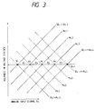
- Fig. 3 is a diagram showing the relation between the analog input signal and voltages at respective nodes in the voltage divider of Fig. 1.
- Fig. 4 is a block diagram of the higher-order logical circuit of Fig. 1.
- Fig. 5 is a diagram of a serial-parallel type A/D converter according to a second embodiment of this invention.
- Fig. 6 is a diagram showing the output voltages from a pair of the sample circuits of Fig. 5.
- Fig. 7 is a diagram showing the contents of a conversion time in the A/D converter of Fig. 5.
- Fig. 8 is a diagram of a serial-parallel type A/D converter according to a third embodiment of this invention.
- Fig. 9 is a diagram showing the contents of a conversion time in the A/D converter of Fig. 8.
- Fig. 10 is a diagram of a serial-parallel type A/D converter according to a fourth embodiment of this invention.
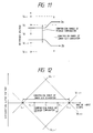
- Fig. 11 is a diagram showing a comparison range of the higher-order comparator, and a conversion range of the lower-order A/D conversion circuit in the A/D converter of Fig. 10.
- Fig. 12 is a diagram showing the relation between the analog input signal and the selected differential output voltages in the A/D converter of Fig. 10.
- Fig. 13 is a diagram of a serial-parallel type A/D converter according to a fifth embodiment of this invention.
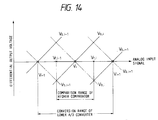
- Fig. 14 is a diagram showing the relation between the analog input signal and the selected differential output voltages in the A/D converter of Fig. 13.
- Fig. 15 is a diagram of a serial-parallel type A/D converter according to a sixth embodiment of this invention.
- Fig. 16 is a diagram of a serial-parallel type A/D converter according to a seventh embodiment of this invention.
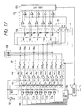
- Fig. 17 is a diagram of a serial-parallel type A/D converter according to an eighth embodiment of this invention.
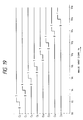
- Fig. 18 is a diagram showing the relation between the analog input signal and the output currents from the differential conversion circuits in the A/D converter of Fig. 17.
- Fig. 19 is a diagram showing the relation between the analog input signal and the output signals from the higher-order comparators in the A/D converter of Fig. 17.
- Fig. 20 is a diagram showing the relation between the analog input signal and the states of the switches in the A/D converter of Fig. 17.
- Fig. 21 is a diagram showing conditions of the lower-order A/D conversion in the A/D converter of Fig. 17.
- Fig. 22 is a diagram showing conditions of the lower-order A/D conversion over the entire range of the analog input signal in the A/D converter of Fig. 17.
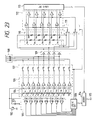
- Fig. 23 is a diagram of a serial-parallel type A/D converter according to a ninth embodiment of this invention.
- Fig. 24 is a diagram of a serial-parallel type A/D converter according to a tenth embodiment of this invention.
- Fig. 25 is a diagram of a serial-parallel type A/D converter according to an eleventh embodiment of this invention.
- Fig. 26 is a block diagram of the conversion logical circuit of Fig. 25.
- Fig. 27 is a diagram of a serial-parallel type A/D converter according to a twelfth embodiment of this invention.
- Fig. 28 is a diagram of part of the A/D converter of Fig. 10.
- Fig. 29 is a block diagram of the higher-order logical circuit of Fig. 10.
- Fig. 30 is a diagram of part of the A/D converter of Fig. 13.
- Fig. 31 is a block diagram of the higher-order logical circuit of Fig. 13.
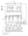
- a serial-parallel type A/D converter includes a set 1 of differential conversion circuits A0-A4 generally composed of differential amplifiers. First input terminals of the differential conversion circuits A0-A4 are subjected to an analog input signal 2. Second input terminals of the differential conversion circuits A0-A4 are subjected to predetermined reference voltages V0-V4 respectively. The reference voltages V0-V4 are separated by equal intervals.
- a reference voltage source 3 applies the reference voltage V0 to the differential conversion circuit A0.
- a voltage divider 4 including a series combination of equal resistors R1-R4 is connected to the reference voltage source 3, and divides the reference voltage V0 and thereby generates the reference voltages V1-V3 applied to the respective differential conversion circuits A1-A3.
- the reference voltage V4 applied to the differential conversion circuit A4 equals a ground potential which agrees with the potential at the negative terminal of the reference voltage source 3.
- the differential conversion circuits A0-A4 generate non-inverted output voltages Va,0-Va,4 and also inverted output voltages Vb,0-Vb,4 which depend on the subtractions between the voltage of the analog input signal 2 and the reference voltages V0-V4 respectively.
- a set 5 of higher-order comparators C0-C4 is connected to the differential conversion circuit set 1. Specifically, first input terminals of the higher-order comparators C0-C4 are connected to non-inverted output terminals of the differential conversion circuits A0-A4 respectively, while second input terminals of the higher-order comparators C0-C4 are connected to inverted output terminals of the differential conversion circuits A0-A4 respectively.
- the higher-order comparators C0-C4 compare the non-inverted output voltages Va,0-Va,4 from the differential conversion circuits A0-A4 with the inverted output voltages Vb,0-Vb,4 from the differential conversion circuits A0-A4, and generate binary signals which represent the results of the related comparisons respectively.
- a higher-order logical circuit 6 is connected to the higher-order comparators C0-C4.
- the higher-order logical circuit 6 receives the binary signals from the higher-order comparators C0-C4 and converts them into a corresponding parallel-form digital signal 7 which forms a higher-order part of a final digital signal.
- the higher-order logical circuit 6 generates a multi-bit selection signal in response to the binary signals from the higher-order comparators C0-C4.
- a set 8 of switches Sa,0-Sa,4 and Sb,0-Sb,4 is connected between the differential conversion circuit set 1 and a voltage divider 9.
- each of the switches Sa,0-Sa,4 and Sb,0-Sb,4 has a switching part, and two terminals which can be connected to and disconnected from each other by the switching part.
- First terminals of the switches Sa,0-Sa,4 are connected to the non-inverted output terminals of the differential conversion circuits A0-A4 respectively.
- Second terminals of the switches Sa,0, Sa,2, and Sa,4 are connected to a first end of a first segment of the voltage divider 9 which includes a series combination of equal resistors R11-R14.
- Second terminals of the switches Sa,1 and Sa,3 are connected to a second end of the first segment of the voltage divider 9.
- First terminals of the switches Sb,0-Sb,4 are connected to the inverted output terminals of the differential conversion circuits A0-A4 respectively.
- Second terminals of the switches Sb,0, Sb,2, and Sb,4 are connected to a first end of a second segment of the voltage divider 9 which includes a series combination of equal resistors R21-R24.
- Second terminals of the stitches Sb,1 and Sb,3 are connected to a second end of the second segment of the voltage divider 9.
- the switch set 8 is connected to the higher-order logical circuit 6 to receive the selection signal from the higher-order logical circuit 6.
- the switches Sa,0-Sa,4 and Sb,0-Sb,4 are controlled by the selection signal fed from the higher-order logical circuit 6.
- One of the switches Sa,0, Sa,2, and Sa,4 and one of the switches Sa,1 and Sa,3 are closed by the selection signal so that one of the non-inverted output voltages Va,0, Va,2, and Va,4 and one of the non-inverted output voltages Va,1 and Va,3 from the differential conversion circuits A0-A4 are selected and transmitted to the opposite ends of the first segment of the voltage divider 9.
- one of the switches Sb,0, Sb,2, and Sb,4 and one of the switches Sb,1 and Sb,3 are closed by the selection signal so that one of the inverted output voltages Vb,0, Vb,2, and Vb,4 and one of the inverted output voltages Vb,1 and Vb,3 from the differential conversion circuits A0-A4 are selected and transmitted to the opposite ends of the second segment of the voltage divider 9.
- the voltages at the first and second ends of the first segment of the voltage divider 9 are denoted by the characters va,0 and va,4 respectively.
- the first segment of the voltage divider 9 divides the resultant potential thereacross and thus generates voltages va,1-va,3 which appear at respective nodes between the resistors R11-R14 and which reside between the voltages va,0 and va,4.
- the voltages va,0-va,4 are separated by equal intervals.
- the voltages at the first and second ends of the second segment of the voltage divider 9 are denoted by the characters vb,0 and vb,4 respectively.
- the second segment of the voltage divider 9 divides the resultant potential thereacross and thus generates voltages vb,1-vb,3 which appear at respective nodes between the resistors R21-R24 and which reside between the voltages vb,0 and vb,4.
- the voltages vb,0-vb,4 are separated by equal intervals.
- a set 10 of lower-order comparators C10-C14 and C20-C23 is connected to the voltage divider 9.
- the voltages vb,0-vb,4 are applied to first input terminals of the lower-order comparators C10-C14 respectively.
- the voltages va,0-va,4 are applied to second input terminals of the lower-order comparators C10-C14 respectively.
- the voltages vb, 0-vb,3 are applied to first input terminals of the lower-order comparators C20-C23 respectively.
- the voltages va,1-va,4 are applied to second input terminals of the lower-order comparators C20-C23 respectively.
- Each of the lower-order comparators C10-C14 and C20-C23 compares the two voltages applied to its first and second input terminals, and generates a binary signal representing the result of the related comparison.
- a lower-order logical circuit 11 is connected to
- the lower-order logical circuit 11 receives the binary signals from the lower-order comparators C10-C14 and C20-C23 and converts them into a corresponding parallel-form digital signal 12 which forms a lower-order part of a final digital signal.
- the lower-order logical circuit 11 has an encoder which can be of a conventional design.
- Fig. 2 shows the relation between the analog input signal 2 and the output signals from the differential conversion circuits A0-A4, the relation between the analog input signal and the output signals from the higher-order comparators C0-C4, and the relation between the analog input signal and the states of the switches Sa,0-Sa,4 and Sb,0-Sb,4.
- the output signals from the comparators C0-C4 are also denoted by the characters C0-C4 for an easy understanding.
- the non-inverted output voltages Va,0-Va,4 and the inverted output voltages Vb,0-Vb,4 vary linearly with the differences between the voltage Vs of the analog input signal 2 and the respective reference voltages V0-V4 at opposite slopes.
- the differential conversion circuit set 1 and the higher-order comparator set 5 cooperate to serve as comparators for comparing the voltage Vs of the analog input signal 2 with the respective reference voltages V0-V4.
- Vs of the analog input signal 2 when the voltage Vs of the analog input signal 2 is higher than the greatest reference voltage V0, all the binary output signals from the higher-order comparators C0-C4 are "0".
- the voltage Vs of the analog input signal 2 resides between the greatest reference voltage V0 and the second greatest reference voltage V1
- only the binary output signal from the higher-order comparator C0 is "1" while the others are "0".
- the selection signal fed from the higher-order logical circuit 6 to the switch set 8 has five bits.
- the stitches Sa,0 and Sb,0 are controlled by a first bit of the selection signal.
- the higher-order logical circuit 6 generates the first bit of the selection signal in agreement with an AND operation between the binary output signal from the higher-order comparator C0 and an inversion of the binary output signal from the higher-order comparator C1.
- the switches Sa,0 and Sb,0 are controlled in response to the AND operation between the binary output signal from the higher-order comparator C0 and the inversion of the binary output signal from the higher-order comparator C1.
- the switches Sa,1 and Sb,1 are controlled by a second bit of the selection signal.
- the higher-order logical circuit 6 generates the second bit of the selection signal in agreement with an AND operation between the binary output signal from the higher-order comparator C0 and an inversion of the binary output signal from the higher-order comparator C2.
- the switches Sa,1 and Sb,1 are controlled in response to the AND operation between the binary output signal from the higher-order comparator C0 and the inversion of the binary output signal from the higher-order comparator C2.
- the switches Sa,2 and Sb,2 are controlled by a third bit of the selection signal.
- the higher-order logical circuit 6 generates the third bit of the selection signal in agreement with an AND operation between the binary output signal from the higher-order comparator C1 and an inversion of the binary output signal from the higher-order comparator C3.
- the switches Sa,2 and Sb,2 are controlled in response to the AND operation between the binary output signal from the higher-order comparator C1 and the inversion of the binary output signal from the higher-order comparator C3.
- the switches Sa,3 and Sb,3 are controlled by a fourth bit of the selection signal.
- the higher-order logical circuit 6 generates the fourth bit of the selection signal in agreement with an AND operation between the binary output signal from the higher-order comparator C2 and an inversion of the binary output signal from the higher-order comparator C4.
- the switches Sa,3 and Sb,3 are controlled in response to the AND operation between the binary output signal from the higher-order comparator C2 and the inversion of the binary output signal from the higher-order comparator C4.
- the switches Sa,4 and Sb,4 are controlled by a fifth bit of the selection signal.
- the higher-order logical circuit 6 generates the fifth bit of the selection signal in agreement with an AND operation between the binary output signal from the higher-order comparator C3 and an inversion of the binary output signal from the higher-order comparator C4.
- the switches Sa,4 and Sb,4 are controlled in response to the AND operation between the binary output signal from the higher-order comparator C3 and the inversion of the binary output signal from the higher-order comparator C4.
- a first member of a pair of selected differential conversion circuits is subjected to the lowest of the reference voltages which are higher than the voltage Vs of the analog input signal 2, and a second member of the pair is subjected to the highest of the reference voltages which are lower than the voltage Vs of the analog input signal 2.
- Fig. 3 shows the relation between the voltage Vs of the analog input signal 2 and the voltages va,0-va,4 and vb,0-vb,4 generated in the voltage divider 9.
- Vi and Vi+1 denote the reference voltages applied to a pair of adjacent higher-order comparators whose outputs are selected and fed to the voltage divider 9 by the switch set 8.
- the difference between the reference voltages Vi and Vi+1 are divided into four equal intervals separated at points v2, v4, and v6.
- the lower-order comparators C10-C14 provide detection of the analog input signal 2 with a resolution determined by the size of these divided intervals.
- the difference between the reference voltages Vi and Vi+1 are divided into intervals separated at points v1, v3, v5, and v7.
- the lower-order comparators C20-C23 provide detection of the analog input signal 2 with a resolution determined by the size of these divided intervals.
- the intervals separated at the points v2, v4, and v6 are offset with the intervals separated at the points v1, v3, v5, and v7, so that the difference between the reference voltages Vi and Vi+1 are divided into eight equal intervals separated at the points v1-v7.
- the lower-order comparators C10-C14 and the lower-order comparators C20-C23 cooperate to provide A/D conversion with a resolution determined by the size of these eight intervals.
- the higher-order logical circuit 6 includes a set of AND gates 60-64.
- First and second input terminals of the AND gate 60 are subjected to the output signals from the higher-order comparators C0 and C1 respectively.
- First and second input terminals of the AND gate 61 are subjected to the output signals from the higher-order comparators C0 and C2 respectively.
- First and second input terminals of the AND gate 62 are subjected to the output signals from the higher-order comparators C1 and C3 respectively.
- First and second input terminals of the AND gate 63 are subjected to the output signals from the higher-order comparators C2 and C4 respectively.
- First and second input terminals of the AND gate 64 are subjected to the output signals from the higher-order comparators C3 and C4 respectively.
- Each of the AND gates 60-64 is of the type having an inverter at its second input terminal.
- the output signal from the AND gate 60 is fed to the switches Sa,0 and Sb,0 as a selection signal.
- the output signal from the AND gate 61 is fed to the switches Sa.1 and Sb,1 as a selection signal.
- the output signal from the AND gate 62 is fed to the switches Sa,2 and Sb,2 as a selection signal.
- the output signal from the AND gate 63 is fed to the switches Sa,3 and Sb,3 as a selection signal.
- the output signal from the AND gate 64 is fed to the switches Sa,4 and Sb,4 as a selection signal.
- the output signals from the AND gates 61 and 62 are applied to first and second input terminals of an AND gate 65.
- the output signals from the AND gates 62 and 63 are applied to first and second input terminals of an AND gate 66.
- the output signals from the AND gates 64 and 66 are applied to first and second input terminals of an OR gate 67 respectively.
- the output signals from the AND gates 64 and 65 are applied to first and second input terminals of an OR gate 68 respectively.
- the output signals from the OR gates 67 and 68 constitute the digital output signal 7 from the logical circuit 6. Specifically, the output signal from the OR gate 67 forms the MSB of the final digital signal. The output signal from the OR gate 68 forms the subsequent bit of the final digital signal.
- This embodiment dispenses with adjustment points so that this embodiment can be easily formed by a monolithic IC.
- relative gain accuracies of the differential conversion circuits A0-A4 are necessary, absolute gain accuracies thereof are unnecessary.
- the differential conversion circuits A0-A4 can be of a simple structure.
- the differential conversion circuits A0-A4 have the additional function of removing common-mode noise such as power supply noise.
- Fig. 5 shows a second embodiment of this invention which is similar to the embodiment of Figs. 1-4 except that a set 17 of sample circuits is added between a differential conversion circuit set 1 and a switch set 8, and between the differential conversion circuit set 1 and a higher-order comparator set 5.
- the sample circuit set 17 samples and holds the non-inverted and inverted output signals from the differential conversion circuit set 1 in response to a sample pulse signal generated by a suitable circuit (not shown).
- the sample circuits can be composed of a simple structure including circuits such as MOS analog switches and source follower circuits.
- VA and VB denote the non-inverted voltage and the inverted voltage inputted into a voltage divider 9 respectively.
- a conversion time is divided into first to fifth periods.
- the first is a tracking period during which the sample circuits follow the input signals.
- the second is a period for settling the sample circuits.
- the third is a period for settling the output signals from the switches. Until the end of the third period, the signals from the higher-order comparator set 5 are inputted into and processed by a higher-order logical circuit 6 and a selection signal is generated to settle the signals selected by the switches.
- the fourth is a period for settling the input signals into a lower-order comparator set 10.
- the fifth is a period which lasts between the moment of the generation of the output signals from the lower-order comparator set 10 and the moment of the generation of the output signal from a lower-order logical circuit 11.
- Fig. 8 shows a third embodiment of this invention which is similar to the embodiment of Figs. 5-7 except that a set 20 of sample circuits is added between a switch set 8 and a voltage divider 9.
- the sample circuit set 20 samples and holds the signals fed from the switch set 8 to the voltage divider 9 in response to a sample pulse signal generated by a suitable circuit (not shown).
- a conversion time is divided into first to third periods.
- the first is a tracking period during which the sample circuits follow the input signals.
- the signals inputted into a lower-order comparator set 10 are settled.
- the first period corresponds to both of the first and fourth periods of Fig. 7.
- the second is a period for settling the sample circuits.
- a lower-order part of the result of the A/D conversion is outputted.
- the second period corresponds to both of the second and fifth periods of Fig. 7.
- the third is a period for settling the output signals from the switches. Until the end of the third period, the signals from a higher-order comparator set 5 are inputted into and processed by a higher-order logical circuit 6 and a selection signal is generated to settle the signals selected by the switch set 8.
- Figs. 10 and 28 show a fourth embodiment of this invention which is similar to the embodiment of Figs. 1-4 except for design changes indicated hereinafter.
- a set 22 of higher-order comparators are exposed to an analog input signal 2 and different reference voltages generated by a combination of a reference voltage source 3 and a voltage divider 21. Specifically, first input terminals of the higher-order comparators in the set 22 are subjected to the analog input signal. Second input terminals of the higher-order comparators in the set 22 are subjected to the reference voltages respectively. The higher-order comparators compare the voltage of the analog input signal with the reference voltages respectively.
- the reference voltages Vr,i applied to the higher-order comparators are exactly intermediate between the reference voltages Vi and the adjacent reference voltages Vi+1 applied to a differential conversion circuit set 1.
- the output signals from the differential conversion circuits subjected to the reference voltages Vi-1 and Vi+1 are selected by a switch set 24 and are transmitted to a lower-order comparator set 26 to be exposed to lower-order A/D conversion.
- the analog input signal resides within a unit comparison range of a higher-order comparator during the higher-order A/D conversion and then moves out of the unit comparison range but remains within a conversion range of a lower-order A/D conversion section during the lower-order A/D conversion as shown by the lines 2a and 2b of Fig. 11.
- the lower-order A/D conversion keeps accurate.
- the higher-order comparator set 22 operates similarly to the operation of the higher-order comparator set in the embodiment of Figs. 1-4, and provides higher-order conversion values. On the basis of the higher-order comparator output signals, four of the differential conversion output signals from the differential conversion circuit set 1 are selected.
- Fig. 12 shows condition of the selection of the differential conversion signals.
- the abscissa denotes an analog input signal while the ordinate denotes selected differential output voltages.
- the reference voltages applied to the related differential conversion circuits 1 are represented by Vi-1, Vi, and Vi+1.
- the reference voltages applied to the related higher-order comparators are represented by Vr,i-1 and Vr,i.
- the reference voltage Vr,i-1 is set exactly intermediate between the reference voltages Vi-1 and Vi of the differential conversion circuits.
- the reference voltage Vr,i is set exactly intermediate between the reference voltages Vi and Vi+1 of the differential conversion circuits.
- the differential output voltages from the differential conversion circuits related to the reference voltages Vi-1 and Vi+1 are selected and switched by the switch set 24 so that these two differential output voltages are fed to the voltage divider 25.
- the lower-order A/D conversion is performed similarly to the lower-order A/D conversion in the embodiment of Figs. 1-4.
- the number of lower-order comparators is greater than the number of the lower-order comparators in the embodiment of Figs. 1-4.
- a logical circuit 23 includes a combination of an inverter 23A, an AND gate 23B, and OR gates 23C and 23D, generating selection signals and a higher-order A/D conversion output signal 7 on the basis of the output signals from the higher-order comparators C1 and C2.
- the selection signals are fed to the switch set 24 to control the switch set 24.
- the conversion range of the lower-order A/D conversion differs from the unit comparison range of the higher-order comparators.
- the results of the higher-order A/D conversion and the lower-order A/D conversion are added to obtain a final result of the A/D conversion.
- the lowest bit of the result of the higher-order A/D conversion and the highest bit of the result of the lower-order A/D conversion are overlapped or made in equal positions.
- a lower-order logical circuit 27 following the lower-order comparator set 26 transfers a control signal to the higher-order logical circuit 23 so that the higher-order logical circuit 23 will output an accurate A/D conversion value.
- Figs. 13 and 30 show a fifth embodiment of this invention which is similar to the embodiment of Figs. 10-12 except for design changes indicated hereinafter.
- differential conversion output signals from a differential conversion circuit set 1 are selected, and the selected signals are inputted into a voltage divider 31 as follows.
- Fig. 14 shows conditions of the selection of the differential conversion signals.
- the abscissa denotes an analog input signal while the ordinate denotes selected differential output voltages.
- the analog input signal resides between the reference voltages Vr,i-1 and Vr,i of the higher-order comparators, the three adjacent differential output voltages of the differential conversion circuit set 1 are selected and are changed by a switch set 30 so that the three differential output voltages are fed to a voltage divider 31.
- a logical circuit 13 includes a combination of an inverter 23A, an AND gate 23B, and OR gates 23C and 23D, generating selection signals and a higher-order A/D conversion output signal 7 on the basis of the output signals from the higher-order comparators C1 and C2.
- the selection signals are fed to the switch set 30 to control the switch set 30.
- a lower-order comparator set 32 is divided into first and second parts.
- the first part compares the differential output voltages Va,i-1 and Vb,i-1 of the differential conversion circuit related to the reference voltage Vi-1 with the differential output voltages Va,i and Vb,i of the differential conversion circuit related to the reference voltage Vi.
- the second part compares the differential output voltages Va,i and Vb,i of the differential conversion circuit related to the reference voltage Vi with the differential output voltages Va,i+1 and Vb,i+1 of the differential conversion circuit related to the reference voltage Vi+1.
- the differential output voltages are divided, and finer comparisons are performed in a manner similar to the manner of Fig. 3.
- a comparison output signal from the lower-order comparator set 32 is inputted into a lower-order logical circuit 33, and a lower-order A/D conversion output signal is generated by the lower-order logical circuit 33.
- Fig. 15 shows a sixth embodiment of this invention which is similar to the embodiment of Figs. 10-12 except for the following points.
- a differential conversion circuit set 1 generates differential output currents fed to a switch set 24.
- a set 80 of load resistors is connected to lines between the switch set 24 and a voltage divider 25 to convert the differential currents into corresponding differential voltages which are fed to the voltage divider 25 via buffers 81.
- Fig. 16 shows a seventh embodiment of this invention which is similar to the embodiment of Figs. 13 and 14 except for the following points.
- a differential conversion circuit set 1 generates differential output currents fed to a switch set 30.
- a set 80 of load resistors is connected to lines between the switch set 30 and a voltage divider 31 to convert the differential currents into corresponding differential voltages which are fed to the voltage divider 31 via buffers 81.
- a serial-parallel type A/D converter includes a set 101 of differential conversion circuits each converting a difference between voltages at its two input terminals into a corresponding output current.
- First input terminals of the differential conversion circuit set 101 are subjected in common to an analog input signal 102.
- Second input terminals of the differential conversion circuit set 101 are subjected to reference voltages respectively.
- the reference voltages are generated by dividing a voltage of a reference voltage source 103 by a voltage divider 104 including a series combination of equal resistors.
- First input terminals of comparators in a higher-order comparator set 105 are subjected to voltages at voltage division points of the voltage divider 104 respectively. Second input terminals of the comparators in the higher-order comparator set 105 are subjected in common to the analog input signal 102.
- the comparison output signals from the higher-order comparator set 105 are fed to a higher-order logical circuit 106.
- the output signal from the higher-order logical circuit 106 is determined in dependence upon the comparison signals fed from the higher-order comparator set 105.
- the higher-order logical circuit 106 generates a selection signal in dependence upon the comparison signals fed from the higher-order comparator set 105.
- the selection signal is fed from the higher-order logical circuit 106 to a first switch set 107.
- the first switch set 107 selects four of the output currents from the differential conversion circuit set 101 in response to the selection signal, so that voltages corresponding to the selected output currents are generated at a set 108 of load resistors.
- the generated voltages are fed to a voltage divider 110, and are divided by the voltage divider 110.
- a second switch set 111 selects given ones of the divided voltages in response to the selection signal fed from the logical circuit 106.
- Comparators in a lower-order comparator set 112 compare the divided voltages with the output voltages from the second switch set 111.
- the comparison output signals from the lower-order comparator set 112 are fed to a lower-order logical circuit 113.
- the output signal from the lower-order logical circuit 113 is determined by the comparison signals fed from the lower-order comparator set 112.
- the output signals from the logical circuits 106 and 113 are added by an adder 114, so that an A/D conversion output signal 115 is obtained by the adder 114.
- the reference voltages applied to the differential conversion circuits A0, A2, ⁇ , A18 are denoted by the characters V0, V2, ⁇ , V18 respectively.
- the output currents Ia0, Ia4, ⁇ , Ia16, Ib2, Ib6, ⁇ , Ib18 from the differential conversion circuits are given by the following equations at ranges close to the respective reference voltages.
- Fig. 19 shows the relation between the voltage Vs of the analog input signal 102 and the comparison output signals from the comparators C2-C16 in the higher-order comparator set 105.
- the comparison output signals from the comparators C2-C16 are also denoted by the characters C2-C16 respectively for an easy understanding.
- the comparison output signal from each of the comparators is "1" when the input signal is greater than the related reference voltage.
- the comparison output signals are inputted into the higher-order logical circuit 106, and thereby a higher-order A/D conversion output signal is obtained.
- Fig. 20 shows ON and OFF states of respective switches in the first switch set 107, and conditions of respective switches in the second switch set 111.
- “1” means an ON state
- “0” means an OFF state.
- “+” denotes the connection to a "+” terminal
- “-” denotes the connection to a "-” terminal.
- the differential conversion circuit set 102 generates output currents which are linearly dependent on the voltage level of the analog input signal 101, and the output currents are selectively stitched.
- Lower-order A/D conversion is performed by use of the above-mentioned output currents as follows.
- the output currents from the differential conversion circuit set 101 are transmitted via the first switch set 107 to the load resistor set 108, and are converted into corresponding voltages.
- Fig. 21 shows an example of the relation between the analog input signal 102 and voltages generated at respective nodes in the voltage divider 110.
- the resolution of the lower-order A/D conversion corresponds to three bits and the voltage of the analog input signal 102 resides between V2 and V4.
- the voltage divider 110 includes first and second series combination of equal resistors. The output currents from four selected adjacent differential conversion circuits are converted by the load resistor set 108 into corresponding voltages respectively. The intervals between these voltages are divided by the voltage divider 110 so that divided voltages VA1-VA3 and VB1-VB4 are generated.
- polarity of an increase and a decrease in the voltages VA0-VA4 and the polarity of an increase and a decrease in the voltages VB0-VB4 are uniquely determined by the level of the analog input signal 102.
- Fig. 22 shows conditions of the voltages VA0-VA4 and VB0-M4 over the entire range of the analog input signal 102.
- the minimal voltage range of the higher-order A/D conversion is expanded by a factor of 2, and the 3-bit lower-order A/D conversion is performed.
- Fig. 23 shows a ninth embodiment of this invention which is similar to the embodiment of Figs. 17-22 except that a set 109 of buffers is added between a load resistor set 108 and a voltage divider 110 to prevent unwanted leakage of currents to the voltage divider 110.
- Fig. 24 shows a tenth embodiment of this invention which is similar to the embodiment of Figs. 17-22 except that the load resistor set 108 (see Fig. 17) is removed.
- Fig. 25 shows an eleventh embodiment of this invention which is similar to the embodiment of Figs. 17-22 except for the following design changes.
- a switch set 140 is provided between a voltage divider 104, a voltage divider 110, and a comparator set 150.
- the comparator set 150 is selectively used in higher-order A/D conversion and lower-order A/D conversion in a time division manner. Specifically, during a period of the higher-order A/D conversion, voltages outputted from the voltage divider 104 are fed to the comparator set 150 via the switch set 140. During a period of the lower-order A/D conversion, voltages outputted from the voltage divider 110 are fed to the comparator set 150 via the switch set 140.
- the switch set 140 includes a section corresponding to the second switch set 111 of Fig. 17.
- a conversion logical circuit 160 following the comparator set 150 converts the output signals from the comparator set 150 into a corresponding A/D conversion output signal 115.
- the conversion logical circuit 160 includes logical circuits 160A and 160B receiving the output signals from the comparator set 150.
- the logical circuits 160A and 160B correspond to the logical circuits 106 and 113 of Fig. 17 respectively.
- the conversion logical circuit 160 also includes an adder 160C adding the output signals of the logical circuits 160A and 160B into the A/D conversion output signal 115.
- the adder 160C corresponds to the adder 114 of Fig. 17.
- the conversion logical circuit 160 further includes a section 160D which generates a selection signal in dependence upon an output signal from the logical circuit 160A, and the selection signal is outputted to a first switch set 107 and the switch set 140.
- the switch sets 107 and 140 are controlled by the selection signal fed from the conversion logical circuit 160.
- Fig. 27 shows an eleventh embodiment of this invention which is similar to the embodiment of Figs. 17-22 except for the following design changes.
- the second switch set 111 is removed, and voltages generated at respective nodes of a voltage divider 110 are inputted into comparators of a lower-order comparator set 112.
Claims (10)
- Convertisseur A/N de type série-parallèle, comprenant :- des moyens pour produire une pluralité de différentes tensions de référence, et- un premier circuit (5, 22, 102) de conversion A/N servant à comparer un signal analogique d'entrée avec les tensions de référence pour effectuer une conversion A/N d'ordre supérieur du signal analogique d'entrée,caractérisé par :- un ensemble de circuits (1) de conversion différentielle ayant des premières bornes d'entrée aptes à recevoir en commun ledit signal analogique d'entrée et des secondes bornes d'entrée aptes à recevoir les tensions de référence respectives (V0 - V4), servant à convertir des différences entre les tensions au niveau des première et seconde bornes d'entrée en des signaux analogiques différentiels de sortie (Va0 - Va4, Vb0 - Vb4),- des premiers moyens de sélection (6, 8, 23, 24, 30) réagissant à un résultat de ladite conversion effectuée par le premier circuit de conversion A/N pour choisir au moins deux des signaux différentiels de sortie,- des moyens (9, 25, 31) pour diviser l'intervalle entre les signaux différentiels de sortie choisis et pour produire des signaux divisés en accord avec ladite division, et- un second circuit (10, 26, 32) de conversion A/N comparant les signaux divisés pour effectuer une conversion A/N d'ordre inférieur du signal analogique d'entrée.
- Convertisseur A/N de type série-parallèle selon la revendication 1, comprenant en outre un ensemble de premiers circuits d'échantillonnage (17) servant à échantillonner les signaux différentiels de sortie et à délivrer des signaux différentiels de sortie échantillonnés, et dans lequel le premier moyen de sélection (8) choisit au moins deux des signaux différentiels de sortie échantillonnés en tant que les signaux différentiels de sortie sélectionnés.
- Convertisseur A/N de type série-parallèle selon la revendication 2, comprenant en outre un ensemble de seconds circuits d'échantillonnage (20) servant à échantillonner les signaux différentiels de sortie sélectionnés et à délivrer des seconds signaux différentiels de sortie échantillonnés, et dans lequel ledit moyen de division (9) divise l'intervalle entre les seconds signaux différentiels de sortie échantillonnés et produit des signaux divisés en accord avec ladite division.
- Convertisseur A/N de type série-parallèle selon l'une quelconque des précédentes revendications, dans lequel ledit premier circuit de conversion A/N compare le signal analogique d'entrée avec une tension de référence intermédiaire entre les tensions de référence des circuits de conversion différentielle adjacents pour effectuer la conversion A/N d'ordre supérieur du signal analogique d'entrée.
- Convertisseur A/N de type série-parallèle selon la revendication 1, 2, 3 ou 4, dans lequel ledit premier moyen de sélection choisit au moins deux des signaux différentiels de sortie de sorte qu'un signal différentiel de sortie se situe entre les signaux différentiels de sortie sélectionnés.
- Convertisseur A/N de type série-parallèle selon l'une quelconque des revendications 1 à 4, dans lequel ledit moyen de sélection choisit trois signaux différentiels de sortie adjacents.
- Convertisseur A/N de type série-parallèle selon l'une quelconque des précédentes revendications, comprenant en outre des seconds moyens de sélection (111) pour choisir au moins deux des signaux de sortie sélectionnés par le premier moyen de sélection, et dans lequel ledit second circuit de conversion A/N compare les signaux divisés et les signaux de sortie choisis par le second moyen de sélection pour effectuer la conversion A/N d'ordre inférieur du signal analogique d'entrée.
- Convertisseur A/N de type série-parallèle selon l'une quelconque des précédentes revendications, dans lequel les signaux différentiels de sortie sont des tensions différentielles de sortie.
- Convertisseur A/N de type série-parallèle selon la revendication 1, dans lequel lesdits signaux différentiels de sortie sont des courants différentiels de sortie, et comprenant en outre :- un moyen (108) pour convertir les courants de sortie choisis par le premier moyen de sélection en des tensions de sortie correspondantes,- un second moyen de sélection (111) pour choisir au moins deux des tensions de sortie,ledit second circuit de conversion A/N étant apte à comparer les tensions divisées et les tensions de sortie choisies par le second moyen de sélection pour effectuer la conversion A/N d'ordre inférieur du signal analogique d'entrée.
- Convertisseur A/N de type série-parallèle selon l'une quelconque des précédentes revendications, dans lequel chacun desdits signaux différentiels de sortie délivrés par lesdits circuits de conversion différentielle comprend une composante de signal inversée et une composante de signal non inversée.
Applications Claiming Priority (2)
| Application Number | Priority Date | Filing Date | Title |
|---|---|---|---|
| JP203328/89 | 1989-08-04 | ||
| JP20332889 | 1989-08-04 |
Publications (2)
| Publication Number | Publication Date |
|---|---|
| EP0414389A1 EP0414389A1 (fr) | 1991-02-27 |
| EP0414389B1 true EP0414389B1 (fr) | 1996-11-13 |
Family
ID=16472192
Family Applications (1)
| Application Number | Title | Priority Date | Filing Date |
|---|---|---|---|
| EP90308380A Expired - Lifetime EP0414389B1 (fr) | 1989-08-04 | 1990-07-31 | Convertisseur analogique-numérique de type série-parallèle |
Country Status (4)
| Country | Link |
|---|---|
| US (1) | US5151700A (fr) |
| EP (1) | EP0414389B1 (fr) |
| JP (1) | JPH0666691B2 (fr) |
| DE (1) | DE69029111T2 (fr) |
Families Citing this family (19)
| Publication number | Priority date | Publication date | Assignee | Title |
|---|---|---|---|---|
| IT1229752B (it) * | 1989-05-17 | 1991-09-10 | Sgs Thomson Microelectronics | Convertitore analogico/digitale ad elevata velocita'. |
| GB9007465D0 (en) * | 1990-04-03 | 1990-05-30 | Cambridge Consultants | Analogue to digital converter |
| US5210537A (en) * | 1991-02-08 | 1993-05-11 | Analog Devices, Incorporated | Multi-stage A/D converter |
| KR100259031B1 (ko) * | 1992-09-30 | 2000-06-15 | 이데이 노부유끼 | 아날로그/디지탈 변환 장치 |
| FR2699025B1 (fr) * | 1992-12-04 | 1995-01-06 | Thomson Csf Semiconducteurs | Convertisseur analogique numérique. |
| FR2700084B1 (fr) * | 1992-12-30 | 1995-02-10 | Thomson Csf Semiconducteurs | Convertisseur analogique numérique avec échantillonneur bloqueur distribué. |
| US5387914A (en) * | 1993-02-22 | 1995-02-07 | Analog Devices, Incorporated | Correction range technique for multi-range A/D converter |
| US5450085A (en) * | 1993-08-31 | 1995-09-12 | Advanced Micro Devices, Inc. | Method and apparatus for high speed analog to digital conversion using multiplexed flash sections |
| DE69616214T2 (de) * | 1995-03-24 | 2002-06-27 | Koninkl Philips Electronics Nv | Differenzverstärker mit signalabhängigem offset und vielstufiger dual-residium-analog/digitalwandler damit |
| US5748132A (en) * | 1995-07-17 | 1998-05-05 | Matsushita Electric Industrial Co., Ltd. | Interpolation type A/D converter |
| JP3042423B2 (ja) * | 1996-09-30 | 2000-05-15 | 日本電気株式会社 | 直並列型a/d変換器 |
| FR2768873B1 (fr) * | 1997-09-19 | 1999-12-03 | Thomson Csf | Convertisseur analogique-numerique a circuit de repliement arborescent |
| WO2000014884A1 (fr) * | 1998-09-04 | 2000-03-16 | Koninklijke Philips Electronics N.V. | Convertisseur analogique-numerique a double residu |
| JP2002271201A (ja) * | 2001-03-09 | 2002-09-20 | Fujitsu Ltd | A/d変換器 |
| US6741192B2 (en) * | 2002-07-09 | 2004-05-25 | Matsushita Electric Industrial Co., Ltd. | A/D conversion method for serial/parallel A/D converter, and serial/parallel A/D converter |
| JP4879052B2 (ja) * | 2007-03-16 | 2012-02-15 | 株式会社リコー | A/dコンバータ |
| JP4424406B2 (ja) * | 2007-10-22 | 2010-03-03 | ソニー株式会社 | 直並列型アナログ/デジタル変換器及びアナログ/デジタル変換方法 |
| US9059730B2 (en) * | 2013-09-19 | 2015-06-16 | Qualcomm Incorporated | Pipelined successive approximation analog-to-digital converter |
| DE202016105554U1 (de) * | 2016-10-06 | 2018-01-09 | Tridonic Gmbh & Co Kg | Adaptive Analog-Digital-Umsetzerschaltung |
Citations (1)
| Publication number | Priority date | Publication date | Assignee | Title |
|---|---|---|---|---|
| EP0262664A2 (fr) * | 1986-09-30 | 1988-04-06 | Kabushiki Kaisha Toshiba | Convertisseur analogique numérique |
Family Cites Families (9)
| Publication number | Priority date | Publication date | Assignee | Title |
|---|---|---|---|---|
| US3818246A (en) * | 1971-04-06 | 1974-06-18 | Ibm | Switching circuits particularly useful for analog-to-digital converters |
| US4495472A (en) * | 1982-11-22 | 1985-01-22 | At&T Bell Laboratories | Stable fast-settling voltage reference buffer amplifier |
| JPS6066526A (ja) * | 1983-09-22 | 1985-04-16 | Fujitsu Ltd | A/dコンバ−タ |
| DE3405438A1 (de) * | 1984-02-15 | 1985-08-29 | Siemens AG, 1000 Berlin und 8000 München | Integrierbarer analog/digitalwandler |
| JPS611121A (ja) * | 1984-06-14 | 1986-01-07 | Hitachi Ltd | 符号変換回路 |
| DE3586187T2 (de) * | 1984-07-23 | 1992-12-03 | Nec Corp | Analog-digital-wandler. |
| JPS61120530A (ja) * | 1984-11-15 | 1986-06-07 | Toshiba Corp | アナログ・デジタル変換器 |
| US4745393A (en) * | 1985-09-25 | 1988-05-17 | Hitachi, Ltd | Analog-to-digital converter |
| US4764743A (en) * | 1987-10-26 | 1988-08-16 | The United States Of America As Represented By The Secretary Of The Army | Permanent magnet structures for the production of transverse helical fields |
-
1990
- 1990-07-30 US US07/559,088 patent/US5151700A/en not_active Expired - Lifetime
- 1990-07-31 EP EP90308380A patent/EP0414389B1/fr not_active Expired - Lifetime
- 1990-07-31 DE DE69029111T patent/DE69029111T2/de not_active Expired - Fee Related
- 1990-08-02 JP JP2206102A patent/JPH0666691B2/ja not_active Expired - Fee Related
Patent Citations (1)
| Publication number | Priority date | Publication date | Assignee | Title |
|---|---|---|---|---|
| EP0262664A2 (fr) * | 1986-09-30 | 1988-04-06 | Kabushiki Kaisha Toshiba | Convertisseur analogique numérique |
Also Published As
| Publication number | Publication date |
|---|---|
| DE69029111D1 (de) | 1996-12-19 |
| EP0414389A1 (fr) | 1991-02-27 |
| JPH0666691B2 (ja) | 1994-08-24 |
| JPH03157020A (ja) | 1991-07-05 |
| US5151700A (en) | 1992-09-29 |
| DE69029111T2 (de) | 1997-03-27 |
Similar Documents
| Publication | Publication Date | Title |
|---|---|---|
| EP0414389B1 (fr) | Convertisseur analogique-numérique de type série-parallèle | |
| US6480132B1 (en) | A/D converter with higher speed and accuracy and lower power consumption | |
| JPH05218868A (ja) | 多段型ad変換器 | |
| EP0493443B1 (fr) | CONVERTISSEUR ANALOGIQUE-NUMERIQUE PARALLELE UTILISANT 2?n-1 COMPARATEURS | |
| US7030791B2 (en) | A/D conversion device having input level shift and output correction function | |
| WO1992008288A1 (fr) | Convertisseur analogique-numerique avec circuits d'interpolation a double pliage | |
| EP0418184B1 (fr) | Convertisseur symétrique doublement numérique-analogique | |
| US5539406A (en) | Series-parallel type A-D converter for realizing high speed operation and low power consumption | |
| US4983969A (en) | Successive approximation analog to digital converter | |
| EP0272756B1 (fr) | Convertisseur analogique-numérique | |
| US5313206A (en) | Sub-ranging analogue to digital converter using differential signals and direct current subtraction | |
| US6239733B1 (en) | Current interpolation circuit for use in an A/D converter | |
| JP2001044837A (ja) | ディジタル/アナログ変換回路及びそれを用いたアナログ/ディジタル変換回路 | |
| JP2762969B2 (ja) | 抵抗ストリング型d/a変換器、および直並列型a/d変換器 | |
| JPH0690172A (ja) | アナログデジタル変換回路装置およびアナログデジタル変換方法 | |
| US6288662B1 (en) | A/D converter circuit having ladder resistor network with alternating first and second resistors of different resistance values | |
| EP0251758A2 (fr) | Système de conversion numérique-analogique | |
| JPH10501115A (ja) | 信号に依存するオフセットを有する作動増幅器及びこのような作動増幅器を含むマルチステップ2重残差アナログ−デジタルコンバータ | |
| KR100285064B1 (ko) | 선형성을 향상시키기 위한 멀티플라잉 디지털-아날로그 변환기 | |
| US20010020910A1 (en) | Digital-to-analog converter | |
| US4864304A (en) | Analog voltage signal comparator circuit | |
| JP3182165B2 (ja) | A/d変換回路 | |
| KR0162633B1 (ko) | 아날로그-디지탈 변환기 | |
| JP3181532B2 (ja) | 直並列型a/d変換装置 | |
| Connolly et al. | A monolithic 12b+ sign successive approximation A/D converter |
Legal Events
| Date | Code | Title | Description |
|---|---|---|---|
| PUAI | Public reference made under article 153(3) epc to a published international application that has entered the european phase |
Free format text: ORIGINAL CODE: 0009012 |
|
| 17P | Request for examination filed |
Effective date: 19900807 |
|
| AK | Designated contracting states |
Kind code of ref document: A1 Designated state(s): DE FR GB |
|
| 17Q | First examination report despatched |
Effective date: 19940121 |
|
| GRAG | Despatch of communication of intention to grant |
Free format text: ORIGINAL CODE: EPIDOS AGRA |
|
| GRAH | Despatch of communication of intention to grant a patent |
Free format text: ORIGINAL CODE: EPIDOS IGRA |
|
| GRAH | Despatch of communication of intention to grant a patent |
Free format text: ORIGINAL CODE: EPIDOS IGRA |
|
| GRAA | (expected) grant |
Free format text: ORIGINAL CODE: 0009210 |
|
| AK | Designated contracting states |
Kind code of ref document: B1 Designated state(s): DE FR GB |
|
| ET | Fr: translation filed | ||
| REF | Corresponds to: |
Ref document number: 69029111 Country of ref document: DE Date of ref document: 19961219 |
|
| PLBE | No opposition filed within time limit |
Free format text: ORIGINAL CODE: 0009261 |
|
| STAA | Information on the status of an ep patent application or granted ep patent |
Free format text: STATUS: NO OPPOSITION FILED WITHIN TIME LIMIT |
|
| 26N | No opposition filed | ||
| REG | Reference to a national code |
Ref country code: GB Ref legal event code: IF02 |
|
| PGFP | Annual fee paid to national office [announced via postgrant information from national office to epo] |
Ref country code: FR Payment date: 20030711 Year of fee payment: 14 |
|
| PGFP | Annual fee paid to national office [announced via postgrant information from national office to epo] |
Ref country code: GB Payment date: 20030730 Year of fee payment: 14 |
|
| PGFP | Annual fee paid to national office [announced via postgrant information from national office to epo] |
Ref country code: DE Payment date: 20030807 Year of fee payment: 14 |
|
| PG25 | Lapsed in a contracting state [announced via postgrant information from national office to epo] |
Ref country code: GB Free format text: LAPSE BECAUSE OF NON-PAYMENT OF DUE FEES Effective date: 20040731 |
|
| PG25 | Lapsed in a contracting state [announced via postgrant information from national office to epo] |
Ref country code: DE Free format text: LAPSE BECAUSE OF NON-PAYMENT OF DUE FEES Effective date: 20050201 |
|
| GBPC | Gb: european patent ceased through non-payment of renewal fee |
Effective date: 20040731 |
|
| PG25 | Lapsed in a contracting state [announced via postgrant information from national office to epo] |
Ref country code: FR Free format text: LAPSE BECAUSE OF NON-PAYMENT OF DUE FEES Effective date: 20050331 |
|
| REG | Reference to a national code |
Ref country code: FR Ref legal event code: ST |