EP0418906A2 - Card type integrated circuit applicable to systems with different bits - Google Patents
Card type integrated circuit applicable to systems with different bits Download PDFInfo
- Publication number
- EP0418906A2 EP0418906A2 EP19900118165 EP90118165A EP0418906A2 EP 0418906 A2 EP0418906 A2 EP 0418906A2 EP 19900118165 EP19900118165 EP 19900118165 EP 90118165 A EP90118165 A EP 90118165A EP 0418906 A2 EP0418906 A2 EP 0418906A2
- Authority
- EP
- European Patent Office
- Prior art keywords
- integrated circuit
- bit system
- type integrated
- terminals
- card
- Prior art date
- Legal status (The legal status is an assumption and is not a legal conclusion. Google has not performed a legal analysis and makes no representation as to the accuracy of the status listed.)
- Granted
Links
Images


Classifications
-
- G—PHYSICS
- G06—COMPUTING; CALCULATING OR COUNTING
- G06K—GRAPHICAL DATA READING; PRESENTATION OF DATA; RECORD CARRIERS; HANDLING RECORD CARRIERS
- G06K7/00—Methods or arrangements for sensing record carriers, e.g. for reading patterns
- G06K7/0013—Methods or arrangements for sensing record carriers, e.g. for reading patterns by galvanic contacts, e.g. card connectors for ISO-7816 compliant smart cards or memory cards, e.g. SD card readers
- G06K7/0086—Methods or arrangements for sensing record carriers, e.g. for reading patterns by galvanic contacts, e.g. card connectors for ISO-7816 compliant smart cards or memory cards, e.g. SD card readers the connector comprising a circuit for steering the operations of the card connector
-
- G—PHYSICS
- G06—COMPUTING; CALCULATING OR COUNTING
- G06K—GRAPHICAL DATA READING; PRESENTATION OF DATA; RECORD CARRIERS; HANDLING RECORD CARRIERS
- G06K19/00—Record carriers for use with machines and with at least a part designed to carry digital markings
- G06K19/06—Record carriers for use with machines and with at least a part designed to carry digital markings characterised by the kind of the digital marking, e.g. shape, nature, code
- G06K19/067—Record carriers with conductive marks, printed circuits or semiconductor circuit elements, e.g. credit or identity cards also with resonating or responding marks without active components
- G06K19/07—Record carriers with conductive marks, printed circuits or semiconductor circuit elements, e.g. credit or identity cards also with resonating or responding marks without active components with integrated circuit chips
- G06K19/077—Constructional details, e.g. mounting of circuits in the carrier
- G06K19/07743—External electrical contacts
-
- G—PHYSICS
- G06—COMPUTING; CALCULATING OR COUNTING
- G06K—GRAPHICAL DATA READING; PRESENTATION OF DATA; RECORD CARRIERS; HANDLING RECORD CARRIERS
- G06K7/00—Methods or arrangements for sensing record carriers, e.g. for reading patterns
- G06K7/0013—Methods or arrangements for sensing record carriers, e.g. for reading patterns by galvanic contacts, e.g. card connectors for ISO-7816 compliant smart cards or memory cards, e.g. SD card readers
- G06K7/0047—Methods or arrangements for sensing record carriers, e.g. for reading patterns by galvanic contacts, e.g. card connectors for ISO-7816 compliant smart cards or memory cards, e.g. SD card readers for reading/sensing record carriers having edge contacts
Definitions
- the present invention relates to a card type integrated circuit in the size of a name card which can be used by connecting it to a personal computer, a printer, etc. and stores various memory contents, and a connector used for the integrated circuit.
- a card type integrated circuit comprises a substrate loaded with circuit devices, a frame, a cover, etc. that are assembled into a solid body, so-called an IC card (Integrated Circuit Card). Since the card type integrated circuit can be provided with various functions by selecting a circuit device loaded thereon and is easy to be carried, with expectation for a wide application the integrated circuit has already put to practical use in every field of the industry.
- IC card Integrated Circuit Card
- a terminal section which is electrically connected to a connector is loaded on the end portion of a substrate, while circuit devices, such as a memory, etc. are loaded on the center portion thereof.
- circuit devices such as a memory, etc.
- On the rear face of the substrate there is arranged a frame for reinforcing the substrate and the circuit devices.
- the circuit devices are housed in a recess hole provided on the frame.
- On the back of the frame there is provided a back cover.
- the surface of the substrate, except the terminal section, is coated with an insulating film. Further, on the film coated surface there is provided a metallic surface cover.
- a guide section guiding the card type integrated circuit and a housing section are integrally formed.
- the housing section there are arranged contact pins on a position associated with terminals of the card type integrated circuit.
- a guide protrusion On the guide section there is provided a guide protrusion.
- a card type integrated circuit and a connector connected to the card type integrated circuit such as described above have been developed in two types; a ROM type card and a RAM type card. They are divided into an 8-bit system I/O bus and a 16-bit system I/O bus depending on a configuration of a control section of the main body which uses the card type integrated circuit.
- an interface connector i.e. a two-piece connector, for connecting equipment on the side to be connected to the card type integrated circuit and a data processor.
- memory chips such as a RAM, a one-time PROM, a mask ROM, etc.
- the card type integrated circuit is provided with 34 terminals arrayed in an 8-bit system card or 56 terminals arrayed in a 16-bit system card.
- the 8-bit system card uses a connector having 34 poles in a single row pin, while the 16-bit system card requires a connector having 68 poles in a double row pin. Therefore, there is no compatibility between both cards.
- a card type integrated circuit for an 8-bit system and a 16-bit system includes one or more circuit devices loaded on a substrate and a plurality of terminals connected to the circuit devices through an I/O bus system to input and output data from and to external equipment.
- a connector comprises a guide section provided with a guide groove for guiding the card type integrated circuit and a housing section provided with contact pins for connecting to the terminals of the card type integrated circuit.
- the terminals for signals common to the 8-bit system card and the 16-bit system card are arranged on the central portion and the other terminals for signals dedicated to the 16-bit system card are arranged on both end portions.
- the 8-bit system card and the 16-bit system card can be connected with the same connector.
- the 8-bit system card can also be connected to the connector for the 16-bit system card, specifically, there is no need of using a connector exclusive for the 8-bit system card.
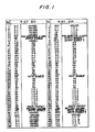
- FIG. 1 there is shown a pin assignment table representative of assignment in terminal arrays on a card type integrated circuit and a connector connected to the card type integrated circuit in accordance with the present invention.
- the memory capacity for the 8-bit system card is set to 1 megabyte as the maximum, while the memory capacity for the 16-bit system card is set to 2 megabytes as the maximum.
- Signals from A0 to A23 and from D0 to D7 used in common for both 8-bit system card and 16-bit system card are collectively arranged on the center portion of the terminal section.
- Signals from D8 to D15 used only for the 16-bit system card are divided into halves to be arranged on both end portions of the terminal section, respectively.
- Vcc and GND for supplying the power are arranged on the outermost portions.
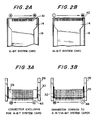
- Card type integrated circuits having terminals consisted of an array as described above and connectors connected to the card type integrated circuits are shown in FIGS. 2A, 2B, 3A, and 3B.
- FIGS. 2A and 2B are plan views representative of essential portions of the card type integrated circuits having terminals consisted of respective arrays as described above.
- FIGS. 3A and 3B are plan views representative of essential portions of the connectors connected to the card type integrated circuits shown in FIGS. 2A and 2B, respectively. Further, FIGS. 2A and 3A show an 8-bit system, while FIGS. 2B and 3B show a 16-bit system.
- terminal sections 41 and 42 there are formed terminal sections 41 and 42 according to respective arrays of a pin assignment table shown in FIG. 1. Specifically, in the 8-bit system card, unused terminal Nos. 1 - 15, 8, 42, 44 - 48 have been deleted, while in the 16-bit system card all the terminals have been assigned.
- a contact pin No. 43 on the unused terminal of the connector is deleted like in case of the 8-bit system card, as if a method of making a 38-pole connector is used. In this way, the connector is made adaptable to the 8-bit system card.
- the connector for the 16-bit system card is structured to have a contact pin No. 44 in the same array order as that of the 16-bit system card.
- the unused terminals on the 8-bit system card type integrated circuit and the connector associated with the 8-bit system card type integrated circuit are deleted in the quantity of each 5 terminals from respective ends on the terminal sections so that stable connection can be achieved without collapsing the balance of the pressure applied on respective pins at the time of insertion.
- a card detecting signal is assigned to a pin No. 6 in common to the 8-bit system card and the 16-bit system card. Consequently, when a system using the 16-bit card system is controlled so as to disregard data on a "HIGH" side (OE2 side), the 8-bit system card can be used even if it is inseted into the same throttle. Further, because there are provided with Vbb terminal and WE terminals (WE1 and WE2), ROM card and RAM card can be used by using the same throttle.
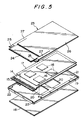
- a card edge type substrate 14 has on one end thereof a terminal section 15 for electrically connecting to a connector which will be described later, and is loaded with a circuit device 16, such as a memory, etc., on a predetermined position.
- the integrated circuit has an insulating film 17 in a size enough to cover the substrate 14 except the terminal section 15, and a rear cover 18.
- the substrate 14 and the circuit device 16 are reinforced and protected by a frame 19 which has a recess hole 20 formed on a position associated with the circuit device 16.
- the frame 19 further includes on a perimeter portion thereof a standing edge 21 which surrounds the substrate 14, the rear cover 18 and a surface cover 23, is formed to be a predetermined height in the direction toward the increasing thickness, and is provided with notched portions 22 on both corner sections of the front end thereof.
- the metallic surface cover 23 possesses a terminal protecting section 24 which covers the terminal section 15 of the substrate 14, receiving sections 25 formed in a V shape on both sides of the terminal protecting section 24, a circuit protecting section 26 which covers, except the terminal section 15, a circuit section covered with the insulating film 17, and leaf spring sections 27 which are formed on both sides of the circuit protecting section 26 to support the terminal protecting section 24.
- the metallic surface cover 23 is made of a sheet metal pressed to form into an entire unity. The components described above are assembled in accordance with the steps below.
- the substrate 14 is fixed on one side of the frame 19 so that the circuit device 16 can fit in the recess hole 20.
- the insulating film 17 is fixed on the substrate 14 in a manner avoiding the terminal section 15, and then the rear cover 18 is adhered to be filed on the other side of the frame 19.
- the circuit protecting section 26 of the surface cover 23 is positioned on the insulating film 17 and a part of the frame 19, while the terminal protecting section 24 and the leaf spring sections 27 are not fixed so as to be separatable from the substrate 14 and the terminal section 15.
- the leaf spring sections 27 of the surface cover 23 are warped beforehand so that the terminal protecting section 24 can closely adhere to the terminal section 15 of the substrate 14.
- the leaf spring sections 27 further include a film similar to the insulating film 17, previously attached on the surface confronting the terminal protecting section 24 as shown with a broken line in FIG. 4. With this film an insulation between the terminal protecting section 24 and the terminal section 15 is kept. In this way, a card type integrated circuit is constructed.
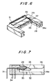
- FIG. 6 is a perspective view showing a connector.
- FIG. 7 is a magnified sectional view representative of an essential portion of the connector shown in FIG. 6.
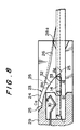
- FIG. 8 is a sectional view showing an essential portion of the connector in a state of being connected to the card type integrated circuit.
- the connector has a guide section 28 provided with a guide groove 28a for guiding the card type integrated circuit, and a housing section 29.
- the guide section 28 and the housing section 29 are formed into a solid body.
- a contact pin positioned so as to associate with the terminal 15 of the card type integrated circuit described above and also, out of the housing section 29 a contact pin 31 which is connected to the contact pin 30 protrudes so as to be connected to another substrate, not shown.
- the contact pin 30 is bent in the housing section 29 to have spring so as to be brought in contact with the terminal 15 when pressed.
- the reference numeral 32 indicates a guide protrusion provided on the rear portion of the guide groove 28a.
- the guide protrusion 32 forms a slope 33 running from the upper surface of the housing section 29 down to the guide section 28 and is integrally connected to a ground terminal 34 on the side of the housing section 29.
- the terminal 15 of the card type integrated circuit is first inserted into the guide groove 28a.
- the tip of the guide protrusion 32 of the connector gets in the notched portions 22 of the frame 19 and then strikes against the top end portions of the receiving sections 25 of the surface cover 23.
- the receiving sections 25 which are bent to be formed into a V shape has the top end portion, as described above, associated with a slope 33 of the guide protrusion 32.
- the receiving sections 25 smoothly slide on the slope 33 while being pushed upward.
- the leaf spring sections 27 are warped upward to raise the terminal protecting section 24 to separate from the terminal 15 of the substrate 14.
- the contact pin 30 When the card type integrated circuit is inserted more deeply into the connector, the contact pin 30 enters between the terminal 15 of the substrate 14 and the terminal protecting section 24 with the result that the contact pin 30 contacts the terminal 15 to complete the insertion of the card type integrated circuit into the connector. Electrical connection between the connector and the card type integrated circuit is completed when the tip of the card type integrated circuit strikes the innermost portion of the housing section 29.
- an interface connector 35 is a two-piece connector for connecting a card type integrated circuit to equipment at the connected side, such as a data processor, etc.
- a memory chip 36 which is connected to the interface connector 35 is a semiconductor memory device consisted of one or more semiconductors capable of loading memory chips, such as a RAM, a one-time PROM, a mask ROM, etc.
- a backup battery 37 retains memory contents stored in a RAM card type integrated circuit.
- a power control circuit 38 is a control circuit which carries out switching operation of the power supplied from respective equipment at the connected side. The power control circuit 38, thus, insures operation of a card type integrated circuit at the time of insertion and removal thereof while the power of the equipment at the connected side is turned on, thereby prevents malfunction that may occur when the power source voltage is in a transit state.
- a write protect switch 39 writes data in a writable card type integrated circuit.
- the write protect switch 39 is so designed that a state of the switch 39 can be read out of equipment at the connected side through an interface.
- a control circuit/chip select circuit 40 is a circuit which selects respective chips when a control circuit, such as the above-mentioned write protect, and a plurality of memory chips are loaded on a card type integrated circuit.
- FIG. 10 shows functions of an online bus system and a pin assignment table representative of assignment of terminals in an array of prior art.
- an 8-bit system card uses a connector having 34 poles in a single row pin, while a 16-bit system card requires a connector having 68 poles in a double row pin. Therefore, there is no compatibility between both cards. Consequently, it is necessary to prepare another connector applicable to the 16-bit system card, causing a remarkable increase in the cost.
- a card type integrated circuit for the 8-bit system card and the 16-bit system card includes one or more circuit devices loaded on a substrate and a plurality of terminals connected to the circuit devices through an I/O bus system to input and output data from and to external equipment.
- a connector has a guide section provided with a guide groove for guiding the card type integrated circuit and a housing section provided with contact pins for connecting to the terminals of the card type integrated circuit.
- the terminals for singnals common to the 8-bit system card and the 16-bit system card are arranged on the central portion and the other terminals for signals dedicated to the 16-bit system card are arranged on both end portions, it is possible to use a single kind of connector in common for connecting to either of the 8-bit system card or the 16-bit system card.
- terminals unnecessary for the 8-bit system card can be removed as shown in FIGS. 2A and 3A, thereby it is possible to further reduce the cost.
- the 6-bit system card can be used thanks to the realization of compatibility. Further, a throttle used in common to a ROM card and a RAM card can be used in respective bus systems. Consequently, an effect of enabling construction of abundant variation of systems can be obtained.
- a card edge having pitches of 1 mm will suffice in respect of restriction to the size of a card type integrated circuit.
- the number of pins may be increased in order from 48 pins.
- face packaging components such as a flat pack IC, etc.
- nearly 70 pins can be used. Where chips are available, there is no need of worry about the capacity.
Abstract
Description
- The present invention relates to a card type integrated circuit in the size of a name card which can be used by connecting it to a personal computer, a printer, etc. and stores various memory contents, and a connector used for the integrated circuit.
- A card type integrated circuit comprises a substrate loaded with circuit devices, a frame, a cover, etc. that are assembled into a solid body, so-called an IC card (Integrated Circuit Card). Since the card type integrated circuit can be provided with various functions by selecting a circuit device loaded thereon and is easy to be carried, with expectation for a wide application the integrated circuit has already put to practical use in every field of the industry.
- When the card type integrated circuit loaded with a memory with a large storage capacity in which programs for electronic equipment are stored is connected to the electronic equipment through connectors, for example, it becomes possible to add new functions to the electronic equipment or to store various types of fonts in the memory to cause a printer to select a desired font for printing.
- Structures of a card type integrated circuit and a connector electrically connected to the card type integrated circuit such as described above have been proposed. For example, there is a disclosure in the Japanese Patent Laid-Open Publication No. 125686/1989.
- In the card type integrated circuit, a terminal section which is electrically connected to a connector is loaded on the end portion of a substrate, while circuit devices, such as a memory, etc. are loaded on the center portion thereof. On the rear face of the substrate, there is arranged a frame for reinforcing the substrate and the circuit devices. The circuit devices are housed in a recess hole provided on the frame. On the back of the frame there is provided a back cover. The surface of the substrate, except the terminal section, is coated with an insulating film. Further, on the film coated surface there is provided a metallic surface cover.
- On the other hand, in the connector a guide section guiding the card type integrated circuit and a housing section are integrally formed. In the housing section there are arranged contact pins on a position associated with terminals of the card type integrated circuit. On the guide section there is provided a guide protrusion. When the card type integrated circuit is inserted into the connection, receiving sections provided on both end portions of the surface cover of the card type integrated circuit with a leaf spring interposed therebetween are pushed upward by the guide protrusion. Thereby, the surface cover is pushed upward to expose the terminal section of the substrate with the result that the contact pins on the connector contact the terminal section. In this way, electrical connection between the card type integrated circuit and the connector is completed.
- A card type integrated circuit and a connector connected to the card type integrated circuit such as described above have been developed in two types; a ROM type card and a RAM type card. They are divided into an 8-bit system I/O bus and a 16-bit system I/O bus depending on a configuration of a control section of the main body which uses the card type integrated circuit.
- In a general card type integrated circuit employing an online bus system, there is provided an interface connector, i.e. a two-piece connector, for connecting equipment on the side to be connected to the card type integrated circuit and a data processor. Connected to the interface connector are memory chips, such as a RAM, a one-time PROM, a mask ROM, etc.
- In such an online bus system, the card type integrated circuit is provided with 34 terminals arrayed in an 8-bit system card or 56 terminals arrayed in a 16-bit system card. The 8-bit system card uses a connector having 34 poles in a single row pin, while the 16-bit system card requires a connector having 68 poles in a double row pin. Therefore, there is no compatibility between both cards.
- Consequently, in addition to a connector used for the 8-bit system card, another connector used for the 16-bit system card becomes in need, which has given rise to a problem of a remarkable increase in the cost.
- It is therefore an object of the present invention to provide a card type integrated circuit which is insured by a common feature and a compatibility between an 8-bit system card and a 16-bit system card and does not cause the cost increase in the case of using the 16-bit card.
- In order to attain the object described above, according to the present invention, a card type integrated circuit for an 8-bit system and a 16-bit system includes one or more circuit devices loaded on a substrate and a plurality of terminals connected to the circuit devices through an I/O bus system to input and output data from and to external equipment.
- According to the present invention, a connector comprises a guide section provided with a guide groove for guiding the card type integrated circuit and a housing section provided with contact pins for connecting to the terminals of the card type integrated circuit. In the layout and assignment of the terminals of the card type integrated circuit and the terminals of the contact pins of the connector, the terminals for signals common to the 8-bit system card and the 16-bit system card are arranged on the central portion and the other terminals for signals dedicated to the 16-bit system card are arranged on both end portions.
- According to the configuration described above, in the card type integrated circuits and the connectors for both 8-bit system and 16-bit system there is no difference in their appearance but only the array of terminals is common to each other. Thus, the 8-bit system card and the 16-bit system card can be connected with the same connector. In other words, the 8-bit system card can also be connected to the connector for the 16-bit system card, specifically, there is no need of using a connector exclusive for the 8-bit system card.
- Further, even in the case of using the connector exclusive for the 8-bit system card, by deleting each five unused terminals exclusive for the 16-bit card from both ends on the terminal section of the connector it is possible to achieve stable connection without collapsing the balance of the pressure applied on respective pins at the time of insertion.
- The objects and features of the present invention will become more apparent from the consideration of the following detailed description taken in conjunction with the accompanying drawings in which:
- FIG. 1 is a table showing pin assignment on the card type integrated circuits and the connectors in accordance with the present invention;
- FIGS. 2A and 2B are plan views showing essential portions of the card type integrated circuits in accordance with the present invention;
- FIGS. 3A and 3B are plan views showing essential portions of the connectors in accordance with the present invention;
- FIG. 4 is a partially broken perspective view showing the construction of the card type integrated circuit;
- FIG. 5 is a disassembled perspective view showing the card type integrated circuit shown in FIG. 4;
- FIG. 6 is a perspective view showing the connector;
- FIG. 7 is a sectional view showing a magnified esstential portion of the connector shown in FIG. 6;
- FIG. 8 is a sectional view of the connector connected to the card type integrated circuit;
- FIG. 9 is a block diagram demonstrating construction of the card type integrated circuit employing an online bus system; and
- FIG. 10 is a table showing functions of the online bus system and pin assignment on a prior art card type integrated circuit and a prior art connector.
- Illustrative embodiments of the present invention will be described hereunder, making reference to the drawings.
- Referring to FIG. 1, there is shown a pin assignment table representative of assignment in terminal arrays on a card type integrated circuit and a connector connected to the card type integrated circuit in accordance with the present invention.
- Signals used in the figure will be explained hereunder.
- (1) D0 - D15; BIDIRECTIONAL DATA BUS to be used with only 8 bits from D0 to D7 in a single row connector and with 16 bits from D0 to D15 in a double row connector
- (2) A0 - A23; ADDRESS BUSes (Input) which are directly addressable up to 16 megabytes
- (3) CE1 and CE2; CHIP ENABLEs (Input) to turn CE1 to a low level at the time of accessing even bytes (D0 - D7) and CE2 to a low level at the time of accessing odd bytes (D8 - D15)
- (4) OE; OUTPUT ENABLE (Input) which is an active low signal used at the time of reading out data
- (5) WE; WRITE ENABLE(Input) which is an active low signal used at the time of writing data
- (6) RDY/BSY; READY SIGNAL (Output) to be used in a card type integrated circuit loaded with an EEPROM at the time of writing data and to control writing timing
- (7) CD1 and CD2; CARD DETECTs (Output) which are card insertion detecting signals located on both ends of a double row connector and capable of detecting whether or not a card is correctly inserted
- (8) WP; WRITE PROTECT (Output) to output a signal indicative of a switch being in a state of write protect
- (9) Vpp1 and Vpp2; PROGRAM POWER SOURCEs which are power sources for writing data in a one-time ROM, and Vpp1 is used as a power source for writing data in even byte memories (D0 - D7) when the data width is a double row containing 16 bits.
- (10) Vcc and GND; POWER SOURCE and GROUND whose terminals are arranged on positions symmetrical to each other to insure safetiness even at the time of inserting a card in reverse.
- As seen in FIG. 1, in the illustrative embodiment the memory capacity for the 8-bit system card is set to 1 megabyte as the maximum, while the memory capacity for the 16-bit system card is set to 2 megabytes as the maximum.
- Signals from A0 to A23 and from D0 to D7 used in common for both 8-bit system card and 16-bit system card are collectively arranged on the center portion of the terminal section. Signals from D8 to D15 used only for the 16-bit system card are divided into halves to be arranged on both end portions of the terminal section, respectively. On the outside portions of the signals from D8 to D15 there are arranged OE1 and WE1. Further, on the positions adjacent to respective OE1 and WE1 there are arranged OE2 and WE2 in an identifiable manner. Finally, Vcc and GND for supplying the power are arranged on the outermost portions.
- Card type integrated circuits having terminals consisted of an array as described above and connectors connected to the card type integrated circuits are shown in FIGS. 2A, 2B, 3A, and 3B.
- FIGS. 2A and 2B are plan views representative of essential portions of the card type integrated circuits having terminals consisted of respective arrays as described above. FIGS. 3A and 3B are plan views representative of essential portions of the connectors connected to the card type integrated circuits shown in FIGS. 2A and 2B, respectively. Further, FIGS. 2A and 3A show an 8-bit system, while FIGS. 2B and 3B show a 16-bit system.
- As seen in the figures, in the 8-bit system card and the 16-bit system card there are formed
terminal sections - In order to adapt the connector exclusively used for the 8-bit system card to every card, a contact pin No. 43 on the unused terminal of the connector is deleted like in case of the 8-bit system card, as if a method of making a 38-pole connector is used. In this way, the connector is made adaptable to the 8-bit system card.
- Also, in order to make the connector adaptable to the 16-bit system card, the connector for the 16-bit system card is structured to have a contact pin No. 44 in the same array order as that of the 16-bit system card.
- The unused terminals on the 8-bit system card type integrated circuit and the connector associated with the 8-bit system card type integrated circuit are deleted in the quantity of each 5 terminals from respective ends on the terminal sections so that stable connection can be achieved without collapsing the balance of the pressure applied on respective pins at the time of insertion.
- Further, a card detecting signal (CD) is assigned to a pin No. 6 in common to the 8-bit system card and the 16-bit system card. Consequently, when a system using the 16-bit card system is controlled so as to disregard data on a "HIGH" side (OE2 side), the 8-bit system card can be used even if it is inseted into the same throttle. Further, because there are provided with Vbb terminal and WE terminals (WE1 and WE2), ROM card and RAM card can be used by using the same throttle.
- Subsequently, construction of the card type integrated circuit will be described hereunder, making reference to FIGS. 4 and 5.
- In the figures, a card
edge type substrate 14 has on one end thereof aterminal section 15 for electrically connecting to a connector which will be described later, and is loaded with acircuit device 16, such as a memory, etc., on a predetermined position. The integrated circuit has an insulatingfilm 17 in a size enough to cover thesubstrate 14 except theterminal section 15, and arear cover 18. - The
substrate 14 and thecircuit device 16 are reinforced and protected by aframe 19 which has arecess hole 20 formed on a position associated with thecircuit device 16. Theframe 19 further includes on a perimeter portion thereof a standingedge 21 which surrounds thesubstrate 14, therear cover 18 and asurface cover 23, is formed to be a predetermined height in the direction toward the increasing thickness, and is provided with notchedportions 22 on both corner sections of the front end thereof. - The
metallic surface cover 23 possesses aterminal protecting section 24 which covers theterminal section 15 of thesubstrate 14, receivingsections 25 formed in a V shape on both sides of theterminal protecting section 24, acircuit protecting section 26 which covers, except theterminal section 15, a circuit section covered with the insulatingfilm 17, andleaf spring sections 27 which are formed on both sides of thecircuit protecting section 26 to support theterminal protecting section 24. Themetallic surface cover 23 is made of a sheet metal pressed to form into an entire unity. The components described above are assembled in accordance with the steps below. - Firstly, the
substrate 14 is fixed on one side of theframe 19 so that thecircuit device 16 can fit in therecess hole 20. The insulatingfilm 17 is fixed on thesubstrate 14 in a manner avoiding theterminal section 15, and then therear cover 18 is adhered to be filed on the other side of theframe 19. - The
circuit protecting section 26 of thesurface cover 23 is positioned on the insulatingfilm 17 and a part of theframe 19, while theterminal protecting section 24 and theleaf spring sections 27 are not fixed so as to be separatable from thesubstrate 14 and theterminal section 15. - The
leaf spring sections 27 of thesurface cover 23 are warped beforehand so that theterminal protecting section 24 can closely adhere to theterminal section 15 of thesubstrate 14. Theleaf spring sections 27 further include a film similar to the insulatingfilm 17, previously attached on the surface confronting theterminal protecting section 24 as shown with a broken line in FIG. 4. With this film an insulation between the terminal protectingsection 24 and theterminal section 15 is kept. In this way, a card type integrated circuit is constructed. - Next, a connector connected to the card type integrated circuit described above will be explained hereunder, making reference to the drawings.
- FIG. 6 is a perspective view showing a connector. FIG. 7 is a magnified sectional view representative of an essential portion of the connector shown in FIG. 6. FIG. 8 is a sectional view showing an essential portion of the connector in a state of being connected to the card type integrated circuit.
- As seen in the figures, the connector has a
guide section 28 provided with aguide groove 28a for guiding the card type integrated circuit, and ahousing section 29. Theguide section 28 and thehousing section 29 are formed into a solid body. In thehousing section 29 there is a contact pin positioned so as to associate with the terminal 15 of the card type integrated circuit described above and also, out of the housing section 29 acontact pin 31 which is connected to thecontact pin 30 protrudes so as to be connected to another substrate, not shown. Thecontact pin 30 is bent in thehousing section 29 to have spring so as to be brought in contact with the terminal 15 when pressed. - The
reference numeral 32 indicates a guide protrusion provided on the rear portion of theguide groove 28a. Theguide protrusion 32 forms aslope 33 running from the upper surface of thehousing section 29 down to theguide section 28 and is integrally connected to aground terminal 34 on the side of thehousing section 29. - To insert the card type integrated circuit into the connector having the structure mentioned above, the
terminal 15 of the card type integrated circuit is first inserted into theguide groove 28a. When the card type integrated circuit reaches a predetermined position as shown in FIG. 8, the tip of theguide protrusion 32 of the connector gets in the notchedportions 22 of theframe 19 and then strikes against the top end portions of the receivingsections 25 of thesurface cover 23. - The receiving
sections 25 which are bent to be formed into a V shape has the top end portion, as described above, associated with aslope 33 of theguide protrusion 32. Thus, when the card type integrated circuit is inserted further, the receivingsections 25 smoothly slide on theslope 33 while being pushed upward. As a result, theleaf spring sections 27 are warped upward to raise theterminal protecting section 24 to separate from theterminal 15 of thesubstrate 14. - When the card type integrated circuit is inserted more deeply into the connector, the
contact pin 30 enters between the terminal 15 of thesubstrate 14 and theterminal protecting section 24 with the result that thecontact pin 30 contacts the terminal 15 to complete the insertion of the card type integrated circuit into the connector. Electrical connection between the connector and the card type integrated circuit is completed when the tip of the card type integrated circuit strikes the innermost portion of thehousing section 29. - Referring to FIG. 9, there is shown a configuration representative of specifications of a cad type integrated circuit using an on line bus system. In the figure, an
interface connector 35 is a two-piece connector for connecting a card type integrated circuit to equipment at the connected side, such as a data processor, etc. Amemory chip 36 which is connected to theinterface connector 35 is a semiconductor memory device consisted of one or more semiconductors capable of loading memory chips, such as a RAM, a one-time PROM, a mask ROM, etc. - A
backup battery 37 retains memory contents stored in a RAM card type integrated circuit. Apower control circuit 38 is a control circuit which carries out switching operation of the power supplied from respective equipment at the connected side. Thepower control circuit 38, thus, insures operation of a card type integrated circuit at the time of insertion and removal thereof while the power of the equipment at the connected side is turned on, thereby prevents malfunction that may occur when the power source voltage is in a transit state. - A write protect
switch 39 writes data in a writable card type integrated circuit. The write protectswitch 39 is so designed that a state of theswitch 39 can be read out of equipment at the connected side through an interface. - A control circuit/chip
select circuit 40 is a circuit which selects respective chips when a control circuit, such as the above-mentioned write protect, and a plurality of memory chips are loaded on a card type integrated circuit. - FIG. 10 shows functions of an online bus system and a pin assignment table representative of assignment of terminals in an array of prior art.
- In accordance with the prior art shown in FIG. 10, an 8-bit system card uses a connector having 34 poles in a single row pin, while a 16-bit system card requires a connector having 68 poles in a double row pin. Therefore, there is no compatibility between both cards. Consequently, it is necessary to prepare another connector applicable to the 16-bit system card, causing a remarkable increase in the cost.
- On the contrary, in accordance with the present invention, a card type integrated circuit for the 8-bit system card and the 16-bit system card includes one or more circuit devices loaded on a substrate and a plurality of terminals connected to the circuit devices through an I/O bus system to input and output data from and to external equipment. A connector has a guide section provided with a guide groove for guiding the card type integrated circuit and a housing section provided with contact pins for connecting to the terminals of the card type integrated circuit. Since in the layout and assignment of the terminals of the card type integrated circuit and the terminals of the contact pins of the connector, the terminals for singnals common to the 8-bit system card and the 16-bit system card are arranged on the central portion and the other terminals for signals dedicated to the 16-bit system card are arranged on both end portions, it is possible to use a single kind of connector in common for connecting to either of the 8-bit system card or the 16-bit system card.
- Consequently, there is no need of separately forming a 16-bit system card having a configuration different from that of an 8-bit system card. In other words, since only a single kind of connector can be used for both cards, a remarkable cost reduction can be achieved.
- Further, when the connector is used exclusively for the 8-bit system card, terminals unnecessary for the 8-bit system card can be removed as shown in FIGS. 2A and 3A, thereby it is possible to further reduce the cost.
- As described above, even in the 16-bit system card type integrated circuit the 6-bit system card can be used thanks to the realization of compatibility. Further, a throttle used in common to a ROM card and a RAM card can be used in respective bus systems. Consequently, an effect of enabling construction of abundant variation of systems can be obtained.
- In addition, when connecting to a card edge having 48 pins in accordance with the illustrative embodiment of the present invention, a card edge having pitches of 1 mm will suffice in respect of restriction to the size of a card type integrated circuit. When the memory capacity is required to be further increased, the number of pins may be increased in order from 48 pins. Simply considering face packaging components, such as a flat pack IC, etc., it is possible to use a card edge having a pitch size up to 0.65mm. Also, according to calculation, nearly 70 pins can be used. Where chips are available, there is no need of worry about the capacity.
- While the present invention has been described with reference to the particular illustrative embodiments, it is not to be restricted by those embodiments but only by the appended claims. It is to be appreciated that those skilled in the art can change or modify the embodiments without departing from the scope and spirit of the present invention.
Claims (5)
predetermined number of circuit devices (16) loaded on a substrate (14);
a plurality of terminals (15) connected to said circuit devices (16) through an I/O bus system and formed on said substrate (14) for inputting and outputting data from and to external equipment;
CHARACTERIZED IN THAT
said terminals (15) for inputting and outputting data, of which terminals (15) for signals common to said 8-bit system and 16-bit system are arranged on the central portion and the other terminals (15) for signals dedicated to said 16-bit system are arranged on both end portions.
CHARACTERIZED IN THAT
said substrate (14) fixed to a frame (19) and covered with a cover (23) so as to avoid said terminals (15).
CHARACTERIZED IN THAT
said terminals (15) arranged on a position symmetrical to a power terminal (Vcc) and a ground terminal (GND).
CHARACTERIZED IN THAT
said circuit devices (16) includes a ROM;
said terminals (15) assigned with signal terminals (15) exclusive for a RAM card type integrated circuit.
a guide section (28) having a guide groove (28a) for guiding said card type integrated circuit;
a housing section (29) having contact pins (30) connected to said input and output terminals (15) of said card type integrated circuit;
CHARACTERIZED IN THAT
said contact pins (30), of which pins (30) for signals common to said 8-bit system and 16-bit system are arranged on the central portion and the other pins (30) for signals dedicated to said 16-bit system are arranged on both end portions.
Applications Claiming Priority (2)
| Application Number | Priority Date | Filing Date | Title |
|---|---|---|---|
| JP109653/89 | 1989-09-21 | ||
| JP1989109653U JPH0648774Y2 (en) | 1989-09-21 | 1989-09-21 | Card type integrated circuit and connector terminal structure |
Publications (3)
| Publication Number | Publication Date |
|---|---|
| EP0418906A2 true EP0418906A2 (en) | 1991-03-27 |
| EP0418906A3 EP0418906A3 (en) | 1992-08-05 |
| EP0418906B1 EP0418906B1 (en) | 1995-07-26 |
Family
ID=14515742
Family Applications (1)
| Application Number | Title | Priority Date | Filing Date |
|---|---|---|---|
| EP90118165A Expired - Lifetime EP0418906B1 (en) | 1989-09-21 | 1990-09-21 | Card type integrated circuit applicable to systems with different bits |
Country Status (4)
| Country | Link |
|---|---|
| US (1) | US5196994A (en) |
| EP (1) | EP0418906B1 (en) |
| JP (1) | JPH0648774Y2 (en) |
| DE (1) | DE69021157T2 (en) |
Cited By (2)
| Publication number | Priority date | Publication date | Assignee | Title |
|---|---|---|---|---|
| EP0602778A2 (en) * | 1992-11-16 | 1994-06-22 | International Business Machines Corporation | Cartridge for removable or portable circuit cards |
| EP2031547A3 (en) * | 2007-08-31 | 2011-06-01 | Sony Corporation | Card-type peripheral device |
Families Citing this family (33)
| Publication number | Priority date | Publication date | Assignee | Title |
|---|---|---|---|---|
| US5544007A (en) * | 1991-07-19 | 1996-08-06 | Kabushiiki Kaisha Toshiba | Card-shaped electronic device used with an electronic apparatus and having shield plate with conductive portion on a lateral side |
| CA2071381C (en) * | 1991-07-19 | 1998-12-15 | Youji Satou | Electronic apparatus, card-type electronic component used with the electronic apparatus, and electronic system with expanding apparatus for expanding function of electronic apparatus |
| US5404271A (en) * | 1991-07-30 | 1995-04-04 | Kabushiki Kaisha Toshiba | Electronic apparatus having a card storing section formed within a body between a support frame and an upper case of the body and having functional elements mounted between the support frame and a lower case of the body |
| US5504648A (en) * | 1991-09-06 | 1996-04-02 | Kabushiki Kaisha Toshiba | Electronic apparatus and electronic system with expanding apparatus having interlock, ejector, grounding, and lock mechanisms, for expanding function of electronic apparatus |
| JPH06171275A (en) * | 1992-09-29 | 1994-06-21 | Mitsubishi Electric Corp | Ic card and production thereof |
| JPH0798620A (en) * | 1992-11-13 | 1995-04-11 | Seiko Epson Corp | Electronic device and computer using it |
| US5476387A (en) * | 1993-06-07 | 1995-12-19 | Methode Electronics Inc. | Memory card frame and cover kit |
| US5397857A (en) * | 1993-07-15 | 1995-03-14 | Dual Systems | PCMCIA standard memory card frame |
| US7074061B1 (en) | 1993-11-12 | 2006-07-11 | Intel Corporation | Versatile communications connectors |
| US5773332A (en) * | 1993-11-12 | 1998-06-30 | Xircom, Inc. | Adaptable communications connectors |
| US6773291B1 (en) | 1993-11-12 | 2004-08-10 | Intel Corporation | Compliant communications connectors |
| JPH07302318A (en) * | 1994-03-09 | 1995-11-14 | Seiko Epson Corp | Card type electronic device |
| US5470237A (en) * | 1994-06-20 | 1995-11-28 | Elco Corporation | Latch mechanism for joining the cover and connector of a removable memory device |
| JP4341043B2 (en) | 1995-03-06 | 2009-10-07 | 真彦 久野 | I / O expansion device, external storage device, method and apparatus for accessing this external storage device |
| US5627416A (en) * | 1995-07-21 | 1997-05-06 | Itt Corporation | Multi-voltage IC card host |
| US5815120A (en) * | 1996-02-28 | 1998-09-29 | International Business Machines Corporation | Radio frequency local area network adapter card structure and method of manufacture |
| US5980267A (en) * | 1996-06-28 | 1999-11-09 | Intel Corporation | Connector scheme for a power pod power delivery system |
| US5920460A (en) * | 1997-01-11 | 1999-07-06 | Methode Electronics, Inc. | PC card receptacle with integral ground clips |
| US5940275A (en) * | 1997-08-08 | 1999-08-17 | Xircom, Inc. | PCMCIA card frame connector and cover assembly |
| WO1999057674A1 (en) * | 1998-05-01 | 1999-11-11 | Wei Chang | Internet ic card system |
| JP2001175834A (en) * | 1999-12-17 | 2001-06-29 | Toshiba Corp | Card type electronic equipment and its manufacturing method |
| US6402556B1 (en) * | 2000-12-19 | 2002-06-11 | Molex Incorporated | Flexible circuit connector for circuit board applications |
| CN100459490C (en) * | 2003-12-04 | 2009-02-04 | 上海复旦微电子股份有限公司 | Intelligent card for multiple cipher standard and its authorization method |
| US7030316B2 (en) * | 2004-01-30 | 2006-04-18 | Piranha Plastics | Insert molding electronic devices |
| US7330369B2 (en) | 2004-04-06 | 2008-02-12 | Bao Tran | NANO-electronic memory array |
| US7440285B2 (en) | 2006-12-29 | 2008-10-21 | Piranha Plastics, Llc | Electronic device housing |
| TWM314932U (en) * | 2007-01-19 | 2007-07-01 | Tai Twun Entpr Co Ltd | Connector capable of protecting inserted card |
| CN101452537B (en) * | 2007-11-30 | 2011-11-16 | 深圳富泰宏精密工业有限公司 | Chip card fixing device and portable electronic device with the fixing device |
| KR20100030126A (en) * | 2008-09-09 | 2010-03-18 | 삼성전자주식회사 | Memory device and electronic apparatus comprising the same |
| USD637192S1 (en) | 2010-10-18 | 2011-05-03 | Apple Inc. | Electronic device |
| USD709894S1 (en) | 2012-09-22 | 2014-07-29 | Apple Inc. | Electronic device |
| US20140233195A1 (en) * | 2013-02-21 | 2014-08-21 | Kabushiki Kaisha Toshiba | Semiconductor device |
| JP2016058093A (en) * | 2015-10-30 | 2016-04-21 | 日本電気株式会社 | Computer, server, module, and assembly method of computer |
Citations (4)
| Publication number | Priority date | Publication date | Assignee | Title |
|---|---|---|---|---|
| FR2359464A1 (en) * | 1976-07-23 | 1978-02-17 | Steenken Magnetdruck | Identity or credit card, works pass or similar - has programmable non-erasable ROM embedded in plastics lamination |
| GB2021823A (en) * | 1978-05-30 | 1979-12-05 | Intel Corp | Data transfer system |
| EP0195865A2 (en) * | 1985-03-25 | 1986-10-01 | Mips Co., Ltd. | Insertion device connector for, and ic card |
| EP0275091A1 (en) * | 1987-01-14 | 1988-07-20 | Nec Corporation | Card-shaped information storage medium |
Family Cites Families (7)
| Publication number | Priority date | Publication date | Assignee | Title |
|---|---|---|---|---|
| US3702464A (en) * | 1971-05-04 | 1972-11-07 | Ibm | Information card |
| JPS6425686A (en) * | 1987-07-22 | 1989-01-27 | Sharp Kk | Still picture telephone equipment |
| JPH0775030B2 (en) * | 1987-08-07 | 1995-08-09 | 沖電気工業株式会社 | Card type integrated circuit connector |
| JPH0288175A (en) * | 1988-09-21 | 1990-03-28 | Aron Kasei Co Ltd | Shot stock for cleaning |
| US4869672A (en) * | 1989-04-17 | 1989-09-26 | Amp Incorporated | Dual purpose card edge connector |
| US5071371A (en) * | 1990-03-30 | 1991-12-10 | Molex Incorporated | Electrical card edge connector assembly |
| US5061190A (en) * | 1990-08-14 | 1991-10-29 | Ziatech Corporation | Double density backward and forward compatible card edge connector system |
-
1989
- 1989-09-21 JP JP1989109653U patent/JPH0648774Y2/en not_active Expired - Lifetime
-
1990
- 1990-09-19 US US07/584,597 patent/US5196994A/en not_active Expired - Lifetime
- 1990-09-21 DE DE69021157T patent/DE69021157T2/en not_active Expired - Lifetime
- 1990-09-21 EP EP90118165A patent/EP0418906B1/en not_active Expired - Lifetime
Patent Citations (4)
| Publication number | Priority date | Publication date | Assignee | Title |
|---|---|---|---|---|
| FR2359464A1 (en) * | 1976-07-23 | 1978-02-17 | Steenken Magnetdruck | Identity or credit card, works pass or similar - has programmable non-erasable ROM embedded in plastics lamination |
| GB2021823A (en) * | 1978-05-30 | 1979-12-05 | Intel Corp | Data transfer system |
| EP0195865A2 (en) * | 1985-03-25 | 1986-10-01 | Mips Co., Ltd. | Insertion device connector for, and ic card |
| EP0275091A1 (en) * | 1987-01-14 | 1988-07-20 | Nec Corporation | Card-shaped information storage medium |
Non-Patent Citations (1)
| Title |
|---|
| PATENT ABSTRACTS OF JAPAN vol. 13, no. 368 (P-919)16 August 1989 & JP-A-1 125 686 ( OKI ELECTRIC ) 18 May 1989 * |
Cited By (3)
| Publication number | Priority date | Publication date | Assignee | Title |
|---|---|---|---|---|
| EP0602778A2 (en) * | 1992-11-16 | 1994-06-22 | International Business Machines Corporation | Cartridge for removable or portable circuit cards |
| EP0602778A3 (en) * | 1992-11-16 | 1994-07-20 | International Business Machines Corporation | Cartridge for removable or portable circuit cards |
| EP2031547A3 (en) * | 2007-08-31 | 2011-06-01 | Sony Corporation | Card-type peripheral device |
Also Published As
| Publication number | Publication date |
|---|---|
| JPH0348884U (en) | 1991-05-10 |
| EP0418906B1 (en) | 1995-07-26 |
| JPH0648774Y2 (en) | 1994-12-12 |
| DE69021157T2 (en) | 1996-04-18 |
| EP0418906A3 (en) | 1992-08-05 |
| DE69021157D1 (en) | 1995-08-31 |
| US5196994A (en) | 1993-03-23 |
Similar Documents
| Publication | Publication Date | Title |
|---|---|---|
| EP0418906B1 (en) | Card type integrated circuit applicable to systems with different bits | |
| US6026007A (en) | Insertable and removable high capacity digital memory apparatus and methods of operation thereof | |
| US7106609B2 (en) | Computer memory cards using flash EEPROM integrated circuit chips and memory-controller systems | |
| US7522424B2 (en) | SmartConnect universal flash media card adapters | |
| US4980856A (en) | IC memory cartridge and a method for providing external IC memory cartridges to an electronic device extending end-to-end | |
| EP1328941B1 (en) | Modular memory device | |
| EP0461623A1 (en) | IC memory card having direct and indirect access card interface functions | |
| JP3078197B2 (en) | IC card reader / writer | |
| JP3154892B2 (en) | IC memory card and inspection method of the IC memory card | |
| KR20050049484A (en) | Smartconnect universal flash media card adapters | |
| US20210103791A1 (en) | Card type solid state drive | |
| EP0379592A1 (en) | Ic memory card | |
| US20070217171A1 (en) | Modular memory device with connector housed controller | |
| JP4564321B2 (en) | Card type electronic equipment | |
| CN113011546A (en) | Universal flash memory card | |
| JPS61120454A (en) | Package of integrated circuit for data memory | |
| KR100741002B1 (en) | Data storage card for universal serial bus standard electronic apparatus | |
| JP2523570B2 (en) | IC card | |
| KR100927768B1 (en) | Portable uss storage | |
| JPH0652376A (en) | Ic memory card | |
| JP3121498B2 (en) | IC card | |
| JP3631320B2 (en) | IC card input / output device and IC card output device | |
| KR20210089283A (en) | Card type solid state drive | |
| JPS63296994A (en) | Portable memory medium | |
| JPS6158093A (en) | Ic card |
Legal Events
| Date | Code | Title | Description |
|---|---|---|---|
| PUAI | Public reference made under article 153(3) epc to a published international application that has entered the european phase |
Free format text: ORIGINAL CODE: 0009012 |
|
| AK | Designated contracting states |
Kind code of ref document: A2 Designated state(s): DE FR GB |
|
| RIN1 | Information on inventor provided before grant (corrected) |
Inventor name: ISHIMIZU, HIDEAKI Inventor name: UCHIDA, TAKAO Inventor name: TANUMA, JIRO |
|
| PUAL | Search report despatched |
Free format text: ORIGINAL CODE: 0009013 |
|
| AK | Designated contracting states |
Kind code of ref document: A3 Designated state(s): DE FR GB |
|
| 17P | Request for examination filed |
Effective date: 19921016 |
|
| 17Q | First examination report despatched |
Effective date: 19941014 |
|
| GRAA | (expected) grant |
Free format text: ORIGINAL CODE: 0009210 |
|
| AK | Designated contracting states |
Kind code of ref document: B1 Designated state(s): DE FR GB |
|
| REF | Corresponds to: |
Ref document number: 69021157 Country of ref document: DE Date of ref document: 19950831 |
|
| ET | Fr: translation filed | ||
| PLBE | No opposition filed within time limit |
Free format text: ORIGINAL CODE: 0009261 |
|
| STAA | Information on the status of an ep patent application or granted ep patent |
Free format text: STATUS: NO OPPOSITION FILED WITHIN TIME LIMIT |
|
| 26N | No opposition filed | ||
| REG | Reference to a national code |
Ref country code: GB Ref legal event code: IF02 |
|
| PGFP | Annual fee paid to national office [announced via postgrant information from national office to epo] |
Ref country code: GB Payment date: 20090916 Year of fee payment: 20 |
|
| PGFP | Annual fee paid to national office [announced via postgrant information from national office to epo] |
Ref country code: DE Payment date: 20090917 Year of fee payment: 20 |
|
| PGFP | Annual fee paid to national office [announced via postgrant information from national office to epo] |
Ref country code: FR Payment date: 20091012 Year of fee payment: 20 |
|
| REG | Reference to a national code |
Ref country code: GB Ref legal event code: PE20 Expiry date: 20100920 |
|
| PG25 | Lapsed in a contracting state [announced via postgrant information from national office to epo] |
Ref country code: GB Free format text: LAPSE BECAUSE OF EXPIRATION OF PROTECTION Effective date: 20100920 |
|
| PG25 | Lapsed in a contracting state [announced via postgrant information from national office to epo] |
Ref country code: DE Free format text: LAPSE BECAUSE OF EXPIRATION OF PROTECTION Effective date: 20100921 |