EP0420113A2 - Apparatus for and method of evaluating multilayer thin films - Google Patents
Apparatus for and method of evaluating multilayer thin films Download PDFInfo
- Publication number
- EP0420113A2 EP0420113A2 EP90118322A EP90118322A EP0420113A2 EP 0420113 A2 EP0420113 A2 EP 0420113A2 EP 90118322 A EP90118322 A EP 90118322A EP 90118322 A EP90118322 A EP 90118322A EP 0420113 A2 EP0420113 A2 EP 0420113A2
- Authority
- EP
- European Patent Office
- Prior art keywords
- light beam
- thin film
- interference light
- multilayer thin
- fourier transform
- Prior art date
- Legal status (The legal status is an assumption and is not a legal conclusion. Google has not performed a legal analysis and makes no representation as to the accuracy of the status listed.)
- Granted
Links
Images


Classifications
-
- G—PHYSICS
- G01—MEASURING; TESTING
- G01B—MEASURING LENGTH, THICKNESS OR SIMILAR LINEAR DIMENSIONS; MEASURING ANGLES; MEASURING AREAS; MEASURING IRREGULARITIES OF SURFACES OR CONTOURS
- G01B11/00—Measuring arrangements characterised by the use of optical techniques
- G01B11/02—Measuring arrangements characterised by the use of optical techniques for measuring length, width or thickness
- G01B11/06—Measuring arrangements characterised by the use of optical techniques for measuring length, width or thickness for measuring thickness ; e.g. of sheet material
- G01B11/0616—Measuring arrangements characterised by the use of optical techniques for measuring length, width or thickness for measuring thickness ; e.g. of sheet material of coating
- G01B11/0675—Measuring arrangements characterised by the use of optical techniques for measuring length, width or thickness for measuring thickness ; e.g. of sheet material of coating using interferometry
Definitions
- the present invention relates to an apparatus for and a method of evaluating a multilayer thin film and more particularly to an apparatus for and a method of evaluating a multilayer thin film capable of evaluating the thickness and the boundary state of each layer of the multilayer thin film formed by epitaxial growth of a semiconductor crystal, for example, in a non-destructive and non-contact manner.
- an interference phenomenon of light is used for measuring the thickness of a thin film in a non-destructive and non-contact manner.
- Numerals 6, 7, 8 and 9 designate one-dimensional reflected light components from the surfaces of the thin film layers 2, 3 and 4 and the substrate 1, respectively.
- the thicknesses and refractive indices of the thin film layers 2, 3 and 4 are designated as (d1,n1), (d2,n2) and (d3,n3) respectively and the refractive index of the substrate 1 is designated as ns.
- the reflected light components 6, 7, 8 and 9 from the surfaces of the respective thin film layers 2, 3 and 4 and the substrate 1 generate phase differences due to each optical path length and are synthesized to interfere with each other on the surface of the sample.
- the i-th thin film layer from the top is defined as the i-th layer (where i is an integer)
- an optical path difference ⁇ i between the reflected light component 6 from the surface of the top layer and the reflected light component at the interface of the i-th layer and the (i+1)-th layer is expressed by the following formula:
- Thickness information of the respective thin film layers 2, 3 and 4 can be obtained by analyzing a spatialgram of a reflected light beam formed by synthesizing the respective reflected light components having the phase differences ⁇ i .
- FTIR method Fourier transform infrared spectroscopic method using Fourier analysis has been proposed as a method of measuring the thickness of a multilayer thin film in a non-destructive and non-contact manner.
- Fig. 2 is a schematic structural view showing an optical system A of an apparatus for evaluating the multilayer thin film using the FTIR method
- Fig. 3 is a general structural diagram of the apparatus.
- an infrared light beam in a predetermined wave number region is emitted from a light source 10.
- the wave number region of the infrared light beam is set according to the crystalline materials constituting the multilayer thin film of a sample 11, for example, at 12000-2000cm ⁇ 1 for AlGaAS series and at 8000-1000cm ⁇ 1 for InGaAsP series.
- the light beam emitted from the light source 10 is transformed into a parallel light beam by an aspherical mirror 12 to be led to a Michelson interferometer 13.
- the Michelson interferometer 13 comprises a beam splitter 14 for splitting the incident parallel light beam into two beams: a transmitted light beam and a reflected light beam, a fixed mirror 15 for reflecting the transmitted light beam of the beam splitter 14, a mobile mirror 16 for reflecting the reflected light beam of the beam splitter 14 and a driver 17 for transferring the mobile mirror 16 at a constant speed in the direction shown by the arrow of Fig. 2.
- the parallel light beam which is incident on the Michelson interferometer 13 is splitted by the beam splitter 14 into two beams: the transmitted light beam and the reflected light beam.
- the transmitted light beam and the reflected light beam return to the beam splitter 14 again and are synthesized to interfere with each other on the surface thereof.
- the transmitted light beam and the reflected light beam are synthesized while continuously varying the optical path differences thereof.
- the interference light to be synthesized on the beam splitter 14 is the light beam modulated with time according to the constant-speed travelling of the mobile mirror 16.
- the interference light beam is led out toward an optical system 18 for lighting the sample 11.
- the interference light beam led to the optical system 18 is converged on the surface of the sample 11 by an aspherical mirror 19 in order to improve the utilization efficiency of light beam energy.
- the light beam reflected by the sample 11 is subject to the interference caused by the film structure of the sample 11 and converged through an aspherical mirror 20 on the light-receiving surface of a photo detector 21.
- an interferogram i.e., a spatialgram including noises
- the interferogram measured by the photo detector 21 is subjected to a Fourier transform by Fourier transform means B to obtain a reflection spectrum.
- filtering means C filters the reflection spectrum to remove wave number regions having no photometric sensitivity therefrom.
- the filtered reflection spectrum is subjected to a reverse Fourier transform by reverse Fourier transform means D to obtain a spatialgram excluding noises.
- Fig. 4 shows an example of the spatialgram provided by the use of the multilayer thin film sample of Fig. 1.
- the abscissa indicates a travelling distance of the mobile mirror 16 and the ordinate indicates an interference intensity of the reflected light beam.
- bursts 22 - 25 which are caused by the mutual intensification of total light due to the interference when the optical path difference by the travelling position of the mobile mirror 16 agrees with the optical path differences of the respective reflected light components indicative of the formula (1).
- the distances between the respective bursts correspond to the optical path differences of the respective reflected light components.
- each side burst 23, 24 and 25 corresponding to the reflected light components 7, 8 and 9 (in Fig.
- Evaluating means E of Fig. 3 can thus analyze the waveform of the aforesaid spatialgram to measure the thicknesses of the respective layers of the multilayer thin film. Furthermore, in addition to the thicknesses of the respective layers, boundary states of the respective layers can be evaluated from the steepnesses of the waveforms of the side bursts 23 - 25, for example.
- an optical system of a converging system is used as the optical system 18 for lighting the sample as described above.
- the purposes of the adoption thereof are, by converging the inference light beam emitted from the Michelson interferometer 13 on the surface of the sample 11, to increase the intensity of the detected light to impinge on the photo detector 21, to improve the SN characteristic of the detection signal thereof, to try to reduce the measurement time, and the like.
- the incident angle ⁇ of the light beam 5 projected on the surface of the sample in Fig. 1 is distributed continuously around this value in practice.
- a variation in transmitted light paths of the respective thin film layers 2 - 4 is generated, and incident wave surfaces are distributed in a certain range.
- the interference intensity is deteriorated and the burst shapes on the spatialgram are blurred and wide, so that a deterioration in resolution, in measurement accuracy and the like is caused.
- the spatialgram shows a quite smooth intensity distribution with respect to the wave number, a slight change in the intensity distribution due to measurement errors and the like results in a change of the waveform of the spatialgram.
- the burst positions are deviated and the adjacent bursts overlap each other, so that a variation in film thickness measured values is caused and the measuring limit thickness of the thin film grows large.
- the reflection spectrum is transformed into the spatialgram in the reverse Fourier transform means D by cosine reverse Fourier transform by means of a cosine term shown in the following formula (3): where R( ⁇ ): reflected light intensity, f( ⁇ ): filtering function, ⁇ : wave number (1/cm), X: distance (cm), and ⁇ s/ ⁇ e: photometrical wave number limits.
- Fig. 5 shows another example of the spatialgram, in which the respective thin film layers 2, 3 and 4 of the sample are 0,503 ⁇ m, 0,314 ⁇ m and 1,136 ⁇ m in thickness respectively. As shown in Fig. 5, burst peaks can be seen in the positions corresponding to the interfaces of the respective layers.
- the burst waveform which appears on the spatialgram can show a reverse phase having upward/downward burst peaks according to filtering conditions (e.g., the form of the filtering function f( ⁇ ) and a filtering wave number region).
- filtering conditions e.g., the form of the filtering function f( ⁇ ) and a filtering wave number region.
- a photometrical wave number range ( ⁇ s - ⁇ e) is a major factor determining the thin film measuring limits.
- the photometrical wave number range mainly determined by a photometrical optical system, it is important to read the peak positions from the burst waveforms on the spatialgram.
- the burst waveforms themselves have an unstable factor of the upward/downward phase, which is a factor providing the thin film thickness measurement with a limitation.
- the present invention is directed to an apparatus for and a method of evaluating a multilayer thin film in which the thickness of the multi layer thin film and the boundary state of each layer are evaluated in a non-destructive and non-contact manner.
- the apparatus for evaluating the multilayer thin film comprises: a first optical system for synthesizing two light beams in a predetermined wave number region while continuously varying optical path differences thereof to produce an interference light beam; a second optical system for projecting onto a multilayer thin film sample the interference light beam emitted from the first optical system as a parallel beam having a predetermined beam diameter, and detecting the interference light beam reflected by the sample to provide an interferogram; Fourier transform means for performing a Fourier transform on the interferogram to provide a reflection spectrum; filtering means for filtering the reflection spectrum; reverse Fourier transform means for performing a reverse Fourier transform on the reflection spectrum filtered to provide a spatialgram; and evaluating means for evaluating the multilayer thin film on the basis of the spatialgram.
- the apparatus for evaluating the multilayer thin film comprises: an optical system for projecting onto a multilayer thin film sample an interference light beam obtained by synthesizing two light beams in a predetermined wave number region while continuously varying optical path differences thereof and detecting the interference light beam reflected by the sample to provide an interferogram; Fourier transform means for performing a Fourier transform on the interferogram to provide a reflection spectrum; filtering means for filtering the reflection spectrum; complex power reverse Fourier transform means for performing complex power reverse Fourier transform on the filtered reflection to provide a spatialgram; and evaluating means for evaluating the multilayer thin film on the basis of the spatialgram.
- the method of evaluating the multilayer thin film comprises: a first step of synthesizing two light beams in a predetermined wave number region while continuously varying optical path differences thereof to produce an interference light beam; a second step of projecting onto a multilayer thin film sample the interference light beam produced in the first step as a parallel beam having a predetermined beam diameter and detecting the interference light beam reflected by the sample to provide an interferogram; a third step of performing a Fourier transform on the interferogram to provide a reflection spectrum; a fourth step of filtering the reflection spectrum; a fifth step of performing a reverse Fourier transform on the filtered reflection spectrum to provide a spatialgram; and a sixth step of evaluating the multilayer thin film on the basis of the spatialgram.
- the method of evaluating the multilayer thin film according to a fourth aspect of the present invention comprises: a first step of projecting onto a multilayer thin film sample an interference light beam obtained by synthesizing two light beams in a predetermined wave number region while continuously varying optical path differences thereof and detecting the interference light beam reflected by the sample to provide an interferogram; a second step of performing a Fourier transform on the interferogram to provide a reflection spectrum; a third step of filtering the reflection spectrum; a fourth step of performing a complex power reverse Fourier transform on the filtered reflection spectrum to provide a spatialgram; and a fifth step of evaluating the multilayer thin film on the basis of the spatialgram.
- an object of the present invention is to provide an apparatus for and a method of evaluating a multilayer thin film capable of evaluating the multilayer thin film more accurately and stably in a non-destructive and non-contact manner.
- the interference light beam is formed into the parallel beam having the predetermined beam diameter and impinges on the sample surface, so that the variation in the incident angle ⁇ with respect to the sample and in the incident surface can be reduced remarkably.
- the transmitted light paths in the multilayer thin film approach an ideal system shown in Fig. 1 infinitely, and the spatialgram to be obtained has accurate information of the multilayer thin film. Therefore, the formulae (1) and (2) can be used in an intact form for the analysis.
- both even and odd functional components in the spatialgram appearing in the limited wave number range of the reflection spectrum can be accurately transformed by the complex transform.
- All burst waveforms on the spatialgram show the same phase by the power transform.
- more information can be introduced in the same photometrical wave number range so that the unstable factor of the burst waveform phase is eliminated. Therefore, the separation accuracy of the burst waveform and the thin film measuring limits are improved.
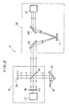
- Fig. 7 is a schematic structural view showing an optical system of an apparatus for evaluating a multilayer thin film according to a first preferred embodiment of the present invention
- Fig. 8 is a general structural diagram thereof.
- the apparatus for evaluating the multilayer thin film comprises a first optical system A1 and a second optical system A2.
- the first optical system A1 is composed of a light source 10, an aspherical mirror 12 and a Michelson interferometer 13, and these components are similar to the corresponding parts of Fig. 2.
- the wave number region of the light source 10 is, however, 32000-0cm ⁇ 1 which is wider than the conventional region.
- the second optical system A2 projects an interference light beam emanating from the Michelson interferometer 13 in the first optical system A1 as a parallel beam having a predetermined beam diameter onto a sample 11 and detects the interference light beam reflected by the sample 11 in a photo detector 21 to provide an interferogram.
- the second optical system A2 comprises an aperture mask 27, plane mirrors 28 and 29, an aspherical mirror 30 and the photo detector 21.
- the interference light beam emanating from the Michelson interferometer 13 is transformed by the aperture mask 27 into a parallel beam having a diameter of several millimeters suited for thin film measurement and is projected through the plane mirror 28 onto the sample 11.
- the light reflected by the sample 11 is regularly reflected by the plane mirror 29 and converged by the aspherical mirror 30 on the light-receiving portion of the photo detector 21 to be transformed into an electric signal therein.
- the interferogram can be measured.
- the interferogram measured by the photo detector 21 is Fourier-transformed by Fourier transform means B so that a reflection spectrum is obtained.
- a cosine reverse Fourier transform is performed thereon by reverse Fourier transform means D to obtain a spatialgram.
- evaluating means E evaluate the thickness of the multilayer thin film and the like.
- a data sampling interval is narrowed to one-fourth and further one-eighth of He-Ne laser wavelength (6328 ⁇ ) for enabling multilayer film separation analysis, although one-half thereof has been conventionally used.
- the spectrum calculation wave number region is expanded to 32000-0cm ⁇ 1.
- the interference light beam emanating from the first optical system A1 is formed into the parallel beam having the predetermined beam diameter and impinges on the surface of the sample 11 by the second optical system A2, so that the variation in the incident angle ⁇ and in the incident surface is remarkably reduced.
- transmitted light paths in the multilayer thin film can approach an ideal system shown in Fig. 1 infinitely, and the spatialgram to be obtained (in Fig. 4) can provide accurate information of the multilayer thin film.
- the thickness and the boundary state of each layer in the multilayer thin film can be evaluated accurately.
- the data sampling interval with respect to the travelling of the mobile mirror 16 is shortened, and the data calculation wave number region is widely expanded. Therefore, the thickness of each layer of the quite thin multilayer film can be accurately analyzed.
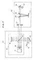
- Fig. 9 is a schematic structural view showing the optical system of the apparatus for evaluating the multilayer thin film according to a second preferred embodiment of the present invention.
- the apparatus comprises the second optical system A2 for projecting the interference light beam emanating from the first optical system A1 onto the sample 11 as a parallel beam having a predetermined beam diameter.
- the second optical system A2 comprises plane mirrors 32, 36, 37, 38 and 39, aspherical mirrors 33, 35 and 40, and an aperture mask 34.
- the interference light beam emanating from the first optical system A1 is, when regularly reflected by the plane mirror 32, converged once by the aspherical mirror 33.
- the converged light beam passes through the aperture mask 34 for improving collimation to be transformed into a parallel beam again by the aspherical mirror 35.
- the parallel beam is projected through the plane mirrors 36 and 37 onto the sample 11.
- the interference light beam reflected by the sample 11 is, when regularly reflected by the plane mirrors 38 and 39, converged on the light-receiving surface of the photo detector 21 by the aspherical mirror 40.
- the other structure of the second preferred embodiment is similar to that of the first preferred embodiment.
- the same effect as the first preferred embodiment can be obtained with the second preferred embodiment.
- Fig. 10 is a schematic structural view showing the optical system of the apparatus for evaluating the multilayer thin film according to a third preferred embodiment of the present invention.
- the apparatus uses an optical system for lighting having a Cassegrain structure as the second optical system A2, whereby the interference light beam emanating from the first optical system A1 can be converged in a wider range to be transformed into a parallel beam.
- the second optical system A2 comprises aspherical mirrors 42 and 46, an aperture mask 43, a converging mirror 44 having an elliptic reflecting surface and a hyperboloidal mirror 45 (or approximatively a convex mirror).
- the interference light beam emanating from the first optical system A1 is converged once by the aspherical mirror 42 and passes through the aperture mask 43 for improving collimation.
- the converging position by the aspherical mirror 42 corresponds to one focus position of the elliptic reflecting surface of the converging mirror 44. In the other focus position thereof the hyperboloidal mirror 45 is disposed.
- the light beam diverged after passing through the aperture mask 43 is converged again by the converging mirror 44 and reflected by the hyperboloidal mirror 45 to be transformed into a parallel beam thereon.
- the parallel beam thus formed is projected onto the sample 11, and the interference light beam reflected by the sample 11 is converged on the light-receiving surface of the photo detector 21 by the aspherical mirror 46.
- the other structure of the third preferred embodiment is similar to that of the first preferred embodiment.
- the same effect as the first preferred embodiment can be obtained with the third preferred embodiment.
- the Fourier-transform spectroscopic analysis is performed solely on the interferogram of the multilayer thin film sample to provide the spatialgram.
- the spatialgram may be provided by the method described hereinafter.
- another interferogram is measured in the same manner as above-mentioned by the use of a standard sample in which gold is deposited on a semiconductor substrate and is stored in a memory.
- the interferogram data of the standard sample are read out from the memory as required and are Fourier-transformed to find the reflection spectrum thereof.
- the reflection spectrum of the standard sample is subtracted from the reflection spectrum of the multilayer thin film sample 11 to find a difference spectrum.
- the difference spectrum is filtered by data processing means to remove noise wave number regions therefrom.
- the reverse Fourier transform is performed on the filtered difference spectrum to obtain the spatialgram.
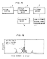
- Fig. 11 is a general structural diagram of the apparatus for evaluating the multilayer thin film according to a fourth preferred embodiment of the present invention.
- the filtered reflection spectrum is transformed by means of complex power reverse Fourier transform means F to provide the spatialgram.
- the complex transform is a common basic technique in Fourier-transform spectroscopy.
- the complex power transform there has been no example which applies the complex power transform to the case where the reflection spectrum is reverse-Fourier-transformed into the spatialgram for the purpose of measuring the thickness of the semiconductor multilayer thin film.
- the complex power reverse Fourier transform means F when the reflection spectrum is reverse-Fourier-transformed into the spatialgram, the complex power transform by means of e(j2 ⁇ x) including a cosine term and a sine term as shown in the following formula (4) is performed: where R( ⁇ ): reflected light intensity, f( ⁇ ): filtering function, ⁇ : wave number (1/cm), X: distance (cm), and ⁇ s/ ⁇ e: photometrical wave number limits.
- the spatialgram obtained by means of the complex power reverse Fourier transform means F according to the present invention is shown in Fig. 12, and the spatialgram obtained by means of the conventional cosine reverse Fourier transform means D is shown in Fig. 6.
- the cosine reverse Fourier transform shown in Fig. 6 since two burst waveforms overlap each other in an unsymmetrical waveform, it is difficult to read the peak positions.
- the unsymmetrical waveform is sensitive to the filtering conditions in the reverse Fourier transform and changes its shape subtly, so that it is practically impossible to find the peaks from this waveform to obtain the film thickness.
- the spatialgram shown in Fig. 12 according to the present invention, although the intervals between the peak positions are about 0,1 ⁇ m, the burst waveforms are obviously separated.
- the spatialgram shown in Fig. 12 is a stable spatialgram sufficient to use for the practical film thickness measurement. Compared with the spatialgram by means of the conventional cosine reverse Fourier transform, since more information is provided in the spatialgram by means of the complex power reverse Fourier transform and each burst wave form becomes the same phase, the measuring accuracy of the film thickness can be improved thereby.
- the first optical system A1 and the second optical system A2 of Fig. 8 may be substituted for the optical system A of Fig. 11.
- the thin film can be measured to the thickness of about 0,1 ⁇ m under the photometrical conditions under which 0,2 ⁇ m is the limit in the apparatus of Fig. 8.
Abstract
Description
- The present invention relates to an apparatus for and a method of evaluating a multilayer thin film and more particularly to an apparatus for and a method of evaluating a multilayer thin film capable of evaluating the thickness and the boundary state of each layer of the multilayer thin film formed by epitaxial growth of a semiconductor crystal, for example, in a non-destructive and non-contact manner.
- Generally, an interference phenomenon of light is used for measuring the thickness of a thin film in a non-destructive and non-contact manner.
- For example, see a sample having semiconductor
thin film layers semiconductor substrate 1 as shown in Fig. 1, on the surface of which apredetermined light beam 5 impinges at an incident angle ϑ.Numerals thin film layers substrate 1, respectively. The thicknesses and refractive indices of thethin film layers substrate 1 is designated as ns. - The
reflected light components thin film layers substrate 1 generate phase differences due to each optical path length and are synthesized to interfere with each other on the surface of the sample. When the i-th thin film layer from the top is defined as the i-th layer (where i is an integer), an optical path difference δi between thereflected light component 6 from the surface of the top layer and the reflected light component at the interface of the i-th layer and the (i+1)-th layer is expressed by the following formula:
thin film layers - In general, a method of evaluating the film thickness from the analysis of an interference fringe of a reflection interference spectrum of the thin film has been conventionally adopted. This method is effective for the film structure consisting of a single layer, however, cannot be practically used for the film structure consisting of plural layers because it is very difficult to separate and analyze each interference fringe.
- Fourier transform infrared spectroscopic method (FTIR method) using Fourier analysis has been proposed as a method of measuring the thickness of a multilayer thin film in a non-destructive and non-contact manner. Fig. 2 is a schematic structural view showing an optical system A of an apparatus for evaluating the multilayer thin film using the FTIR method, and Fig. 3 is a general structural diagram of the apparatus.
- As shown in Figs. 2 and 3, an infrared light beam in a predetermined wave number region is emitted from a
light source 10. The wave number region of the infrared light beam is set according to the crystalline materials constituting the multilayer thin film of asample 11, for example, at 12000-2000cm⁻¹ for AℓGaAS series and at 8000-1000cm⁻¹ for InGaAsP series. - The light beam emitted from the
light source 10 is transformed into a parallel light beam by anaspherical mirror 12 to be led to a Michelsoninterferometer 13. - The Michelson
interferometer 13 comprises abeam splitter 14 for splitting the incident parallel light beam into two beams: a transmitted light beam and a reflected light beam, afixed mirror 15 for reflecting the transmitted light beam of thebeam splitter 14, amobile mirror 16 for reflecting the reflected light beam of thebeam splitter 14 and adriver 17 for transferring themobile mirror 16 at a constant speed in the direction shown by the arrow of Fig. 2. The parallel light beam which is incident on the Michelsoninterferometer 13 is splitted by thebeam splitter 14 into two beams: the transmitted light beam and the reflected light beam. When reflected by the fixed mirror and themobile mirror 16, respectively, the transmitted light beam and the reflected light beam return to thebeam splitter 14 again and are synthesized to interfere with each other on the surface thereof. Since themobile mirror 16 is transferred at a constant speed in the direction shown by the arrow of Fig. 2 by thedriver 17, the transmitted light beam and the reflected light beam are synthesized while continuously varying the optical path differences thereof. Thus, the interference light to be synthesized on thebeam splitter 14 is the light beam modulated with time according to the constant-speed travelling of themobile mirror 16. The interference light beam is led out toward anoptical system 18 for lighting thesample 11. - The interference light beam led to the
optical system 18 is converged on the surface of thesample 11 by anaspherical mirror 19 in order to improve the utilization efficiency of light beam energy. As described above, the light beam reflected by thesample 11 is subject to the interference caused by the film structure of thesample 11 and converged through anaspherical mirror 20 on the light-receiving surface of aphoto detector 21. - Thus an interferogram (i.e., a spatialgram including noises) is measured by the
photo detector 21. The interferogram measured by thephoto detector 21 is subjected to a Fourier transform by Fourier transform means B to obtain a reflection spectrum. Next, filtering means C filters the reflection spectrum to remove wave number regions having no photometric sensitivity therefrom. The filtered reflection spectrum is subjected to a reverse Fourier transform by reverse Fourier transform means D to obtain a spatialgram excluding noises. - Fig. 4 shows an example of the spatialgram provided by the use of the multilayer thin film sample of Fig. 1. In Fig. 4, the abscissa indicates a travelling distance of the
mobile mirror 16 and the ordinate indicates an interference intensity of the reflected light beam. As shown in Fig. 4, in the spatialgram appear bursts 22 - 25 which are caused by the mutual intensification of total light due to the interference when the optical path difference by the travelling position of themobile mirror 16 agrees with the optical path differences of the respective reflected light components indicative of the formula (1). The distances between the respective bursts correspond to the optical path differences of the respective reflected light components. In the example of Fig. 4, each side burst 23, 24 and 25 corresponding to thereflected light components center burst 22 corresponding to thereflected light component 6 from the surface of the sample (or the thin film layer 2). When the distances from the center burst 22 to therespective side bursts mobile mirror 16. Accordingly the following formula can be obtained from the aforesaid formula (1):
- Evaluating means E of Fig. 3 can thus analyze the waveform of the aforesaid spatialgram to measure the thicknesses of the respective layers of the multilayer thin film. Furthermore, in addition to the thicknesses of the respective layers, boundary states of the respective layers can be evaluated from the steepnesses of the waveforms of the side bursts 23 - 25, for example.
- In the conventional apparatus for evaluating the multilayer thin film constructed as above-mentioned, an optical system of a converging system is used as the
optical system 18 for lighting the sample as described above. The purposes of the adoption thereof are, by converging the inference light beam emitted from the Michelsoninterferometer 13 on the surface of thesample 11, to increase the intensity of the detected light to impinge on thephoto detector 21, to improve the SN characteristic of the detection signal thereof, to try to reduce the measurement time, and the like. - Since the
optical system 18 of the converging system is adopted, the incident angle ϑ of thelight beam 5 projected on the surface of the sample in Fig. 1 is distributed continuously around this value in practice. As a result,a variation in transmitted light paths of the respective thin film layers 2 - 4 is generated, and incident wave surfaces are distributed in a certain range. Thus the interference intensity is deteriorated and the burst shapes on the spatialgram are blurred and wide, so that a deterioration in resolution, in measurement accuracy and the like is caused. Particularly in measuring the thin film, because the spatialgram shows a quite smooth intensity distribution with respect to the wave number, a slight change in the intensity distribution due to measurement errors and the like results in a change of the waveform of the spatialgram. As a result, the burst positions are deviated and the adjacent bursts overlap each other, so that a variation in film thickness measured values is caused and the measuring limit thickness of the thin film grows large. - Accordingly the formulae (1) and (2) cannot be used in an intact form. It is necessary to consider the distribution of the incident angle ϑ and deflection characteristics of reflection.
- In the conventional apparatus for evaluating the multilayer thin film, the reflection spectrum is transformed into the spatialgram in the reverse Fourier transform means D by cosine reverse Fourier transform by means of a cosine term shown in the following formula (3):

- Fig. 5 shows another example of the spatialgram, in which the respective
thin film layers - As above-mentioned, since the reflection spectrum is subjected to the cosine reverse Fourier transform having only the cosine term, the burst waveform which appears on the spatialgram can show a reverse phase having upward/downward burst peaks according to filtering conditions (e.g., the form of the filtering function f(σ) and a filtering wave number region). When the film to be measured is thin, the burst wave forms having upward and downward peaks overlap each other as shown in the spatialgram of Fig. 6, for example. As a result, each peak is swallowed up by a synthesized waveform so that it is difficult to read the peak positions.
- In the method of measuring the film thickness by means of the FTIR method, a photometrical wave number range (σs - σe) is a major factor determining the thin film measuring limits. In the framework of the photometrical wave number range mainly determined by a photometrical optical system, it is important to read the peak positions from the burst waveforms on the spatialgram. However, in the prior art, the burst waveforms themselves have an unstable factor of the upward/downward phase, which is a factor providing the thin film thickness measurement with a limitation.
- The present invention is directed to an apparatus for and a method of evaluating a multilayer thin film in which the thickness of the multi layer thin film and the boundary state of each layer are evaluated in a non-destructive and non-contact manner.
- The apparatus for evaluating the multilayer thin film according to a first aspect of the present invention comprises: a first optical system for synthesizing two light beams in a predetermined wave number region while continuously varying optical path differences thereof to produce an interference light beam; a second optical system for projecting onto a multilayer thin film sample the interference light beam emitted from the first optical system as a parallel beam having a predetermined beam diameter, and detecting the interference light beam reflected by the sample to provide an interferogram; Fourier transform means for performing a Fourier transform on the interferogram to provide a reflection spectrum; filtering means for filtering the reflection spectrum; reverse Fourier transform means for performing a reverse Fourier transform on the reflection spectrum filtered to provide a spatialgram; and evaluating means for evaluating the multilayer thin film on the basis of the spatialgram.
- The apparatus for evaluating the multilayer thin film according to a second aspect of the present invention comprises: an optical system for projecting onto a multilayer thin film sample an interference light beam obtained by synthesizing two light beams in a predetermined wave number region while continuously varying optical path differences thereof and detecting the interference light beam reflected by the sample to provide an interferogram; Fourier transform means for performing a Fourier transform on the interferogram to provide a reflection spectrum; filtering means for filtering the reflection spectrum; complex power reverse Fourier transform means for performing complex power reverse Fourier transform on the filtered reflection to provide a spatialgram; and evaluating means for evaluating the multilayer thin film on the basis of the spatialgram.
- The method of evaluating the multilayer thin film according to a third aspect of the present invention comprises: a first step of synthesizing two light beams in a predetermined wave number region while continuously varying optical path differences thereof to produce an interference light beam; a second step of projecting onto a multilayer thin film sample the interference light beam produced in the first step as a parallel beam having a predetermined beam diameter and detecting the interference light beam reflected by the sample to provide an interferogram; a third step of performing a Fourier transform on the interferogram to provide a reflection spectrum; a fourth step of filtering the reflection spectrum; a fifth step of performing a reverse Fourier transform on the filtered reflection spectrum to provide a spatialgram; and a sixth step of evaluating the multilayer thin film on the basis of the spatialgram.
- The method of evaluating the multilayer thin film according to a fourth aspect of the present invention comprises: a first step of projecting onto a multilayer thin film sample an interference light beam obtained by synthesizing two light beams in a predetermined wave number region while continuously varying optical path differences thereof and detecting the interference light beam reflected by the sample to provide an interferogram; a second step of performing a Fourier transform on the interferogram to provide a reflection spectrum; a third step of filtering the reflection spectrum; a fourth step of performing a complex power reverse Fourier transform on the filtered reflection spectrum to provide a spatialgram; and a fifth step of evaluating the multilayer thin film on the basis of the spatialgram.
- Therefore, an object of the present invention is to provide an apparatus for and a method of evaluating a multilayer thin film capable of evaluating the multilayer thin film more accurately and stably in a non-destructive and non-contact manner.
- According to the apparatus for evaluating the multilayer thin film in the first aspect and the method of evaluating the multilayer thin film in the third aspect, the interference light beam is formed into the parallel beam having the predetermined beam diameter and impinges on the sample surface, so that the variation in the incident angle ϑ with respect to the sample and in the incident surface can be reduced remarkably. As a result, the transmitted light paths in the multilayer thin film approach an ideal system shown in Fig. 1 infinitely, and the spatialgram to be obtained has accurate information of the multilayer thin film. Therefore, the formulae (1) and (2) can be used in an intact form for the analysis.
- According to the apparatus for evaluating the multilayer thin film in the second aspect and the method of evaluating the multilayer thin film in the fourth aspect, both even and odd functional components in the spatialgram appearing in the limited wave number range of the reflection spectrum can be accurately transformed by the complex transform. All burst waveforms on the spatialgram show the same phase by the power transform. As a result, compared with the case of performing the cosine reverse Fourier transform, more information can be introduced in the same photometrical wave number range so that the unstable factor of the burst waveform phase is eliminated. Therefore, the separation accuracy of the burst waveform and the thin film measuring limits are improved.
- These and other objects, features, aspects and advantages of the present invention will become more apparent from the following detailed description of the present invention when taken in conjunction with the accompanying drawings.
-
- Fig. 1 is a typical view showing optical paths of a primary reflected light on each layer when a light beam is projected onto a multilayer thin film structure;
- Fig. 2 is a schematic structural view showing an optical system of a conventional apparatus for evaluating a multilayer thin film;
- Fig. 3 is a general structural diagram of the conventional apparatus for evaluating the multilayer thin film;
- Fig. 4 shows an example of a spatialgram obtained by means of a multilayer thin film sample of Fig. 1;
- Figs. 5 and 6 show spatialgrams obtained by a conventional cosine reverse Fourier transform respectively;
- Fig. 7 is a schematic structural view showing an optical system of an apparatus for evaluating a multilayer thin film according to a first preferred embodiment of the present invention;
- Fig. 8 is a general structural diagram of the apparatus for evaluating the multilayer thin film according to the first preferred embodiment of the present invention;
- Fig. 9 is a schematic structural view showing the optical system of the apparatus for evaluating the multilayer thin film according to a second preferred embodiment of the present invention;
- Fig. 10 is a schematic structural view showing the optical system of the apparatus for evaluating the multilayer thin film according to a third preferred embodiment of the present invention;
- Fig. 11 is a general structural diagram of the apparatus for evaluating the multilayer thin film according to a fourth preferred embodiment of the present invention; and
- Fig. 12 shows a spatialgram obtained by a complex power reverse Fourier transform according to the fourth preferred embodiment of the present invention.
- Fig. 7 is a schematic structural view showing an optical system of an apparatus for evaluating a multilayer thin film according to a first preferred embodiment of the present invention, and Fig. 8 is a general structural diagram thereof.
- As shown in Figs. 7 and 8, the apparatus for evaluating the multilayer thin film comprises a first optical system A1 and a second optical system A2.
- The first optical system A1 is composed of a
light source 10, anaspherical mirror 12 and aMichelson interferometer 13, and these components are similar to the corresponding parts of Fig. 2. The wave number region of thelight source 10 is, however, 32000-0cm⁻¹ which is wider than the conventional region. - The second optical system A2 projects an interference light beam emanating from the
Michelson interferometer 13 in the first optical system A1 as a parallel beam having a predetermined beam diameter onto asample 11 and detects the interference light beam reflected by thesample 11 in aphoto detector 21 to provide an interferogram. The second optical system A2 comprises anaperture mask 27, plane mirrors 28 and 29, anaspherical mirror 30 and thephoto detector 21. - The interference light beam emanating from the
Michelson interferometer 13 is transformed by theaperture mask 27 into a parallel beam having a diameter of several millimeters suited for thin film measurement and is projected through theplane mirror 28 onto thesample 11. The light reflected by thesample 11 is regularly reflected by theplane mirror 29 and converged by theaspherical mirror 30 on the light-receiving portion of thephoto detector 21 to be transformed into an electric signal therein. Thus the interferogram can be measured. - The following processings are similar to those of the prior art. That is, the interferogram measured by the
photo detector 21 is Fourier-transformed by Fourier transform means B so that a reflection spectrum is obtained. After the reflection spectrum is filtered to remove wave number regions having no photometric sensitivity therefrom by filtering means C, a cosine reverse Fourier transform is performed thereon by reverse Fourier transform means D to obtain a spatialgram. By the use of the spatialgram thus obtained, evaluating means E evaluate the thickness of the multilayer thin film and the like. - When the Fourier-transform spectroscopic analysis is performed in the apparatus for evaluating the multilayer thin film, a data sampling interval is narrowed to one-fourth and further one-eighth of He-Ne laser wavelength (6328Å) for enabling multilayer film separation analysis, although one-half thereof has been conventionally used. On the other hand, the spectrum calculation wave number region is expanded to 32000-0cm⁻¹.
- Other structure of the apparatus according to the first preferred embodiment of the present invention is similar to that of the conventional apparauts, and hence the same numerals are assigned to the same or corresponding parts and the redundant description thereof is omitted.
- According to the apparatus of this preferred embodiment, the interference light beam emanating from the first optical system A1 is formed into the parallel beam having the predetermined beam diameter and impinges on the surface of the
sample 11 by the second optical system A2, so that the variation in the incident angle ϑ and in the incident surface is remarkably reduced. As a result, transmitted light paths in the multilayer thin film can approach an ideal system shown in Fig. 1 infinitely, and the spatialgram to be obtained (in Fig. 4) can provide accurate information of the multilayer thin film. Hence, the thickness and the boundary state of each layer in the multilayer thin film can be evaluated accurately. In addition, when the Fourier-transform spectroscopic analysis is performed, the data sampling interval with respect to the travelling of themobile mirror 16 is shortened, and the data calculation wave number region is widely expanded. Therefore, the thickness of each layer of the quite thin multilayer film can be accurately analyzed. - Fig. 9 is a schematic structural view showing the optical system of the apparatus for evaluating the multilayer thin film according to a second preferred embodiment of the present invention.
- As shown in Fig. 9, the apparatus comprises the second optical system A2 for projecting the interference light beam emanating from the first optical system A1 onto the
sample 11 as a parallel beam having a predetermined beam diameter. - The second optical system A2 comprises plane mirrors 32, 36, 37, 38 and 39,
aspherical mirrors aperture mask 34. - The interference light beam emanating from the first optical system A1 is, when regularly reflected by the
plane mirror 32, converged once by theaspherical mirror 33. The converged light beam passes through theaperture mask 34 for improving collimation to be transformed into a parallel beam again by theaspherical mirror 35. The parallel beam is projected through the plane mirrors 36 and 37 onto thesample 11. The interference light beam reflected by thesample 11 is, when regularly reflected by the plane mirrors 38 and 39, converged on the light-receiving surface of thephoto detector 21 by theaspherical mirror 40. - The other structure of the second preferred embodiment is similar to that of the first preferred embodiment. The same effect as the first preferred embodiment can be obtained with the second preferred embodiment.
- Fig. 10 is a schematic structural view showing the optical system of the apparatus for evaluating the multilayer thin film according to a third preferred embodiment of the present invention.
- As shown in Fig. 10, the apparatus uses an optical system for lighting having a Cassegrain structure as the second optical system A2, whereby the interference light beam emanating from the first optical system A1 can be converged in a wider range to be transformed into a parallel beam.
- The second optical system A2 comprises
aspherical mirrors aperture mask 43, a convergingmirror 44 having an elliptic reflecting surface and a hyperboloidal mirror 45 (or approximatively a convex mirror). - The interference light beam emanating from the first optical system A1 is converged once by the
aspherical mirror 42 and passes through theaperture mask 43 for improving collimation. The converging position by theaspherical mirror 42 corresponds to one focus position of the elliptic reflecting surface of the convergingmirror 44. In the other focus position thereof thehyperboloidal mirror 45 is disposed. The light beam diverged after passing through theaperture mask 43 is converged again by the convergingmirror 44 and reflected by thehyperboloidal mirror 45 to be transformed into a parallel beam thereon. The parallel beam thus formed is projected onto thesample 11, and the interference light beam reflected by thesample 11 is converged on the light-receiving surface of thephoto detector 21 by theaspherical mirror 46. - The other structure of the third preferred embodiment is similar to that of the first preferred embodiment. The same effect as the first preferred embodiment can be obtained with the third preferred embodiment.
- In the above-mentioned first to third preferred embodiments, the Fourier-transform spectroscopic analysis is performed solely on the interferogram of the multilayer thin film sample to provide the spatialgram. However, the spatialgram may be provided by the method described hereinafter. Prior to the measurement of the interferogram of the multilayer
thin film sample 11, for example, another interferogram is measured in the same manner as above-mentioned by the use of a standard sample in which gold is deposited on a semiconductor substrate and is stored in a memory. The interferogram data of the standard sample are read out from the memory as required and are Fourier-transformed to find the reflection spectrum thereof. The reflection spectrum of the standard sample is subtracted from the reflection spectrum of the multilayerthin film sample 11 to find a difference spectrum. The difference spectrum is filtered by data processing means to remove noise wave number regions therefrom. The reverse Fourier transform is performed on the filtered difference spectrum to obtain the spatialgram. By means of this method, a spatialgram in which the center burst is eliminated can be obtained, thereby the multilayer thin film can be evaluated more accurately. - Fig. 11 is a general structural diagram of the apparatus for evaluating the multilayer thin film according to a fourth preferred embodiment of the present invention.
- In Fig. 11, the reference characters A to C and E designate the same parts as those of the conventional apparatus.
- In the preferred embodiment, the filtered reflection spectrum is transformed by means of complex power reverse Fourier transform means F to provide the spatialgram. The complex transform is a common basic technique in Fourier-transform spectroscopy. However, there has been no example which applies the complex power transform to the case where the reflection spectrum is reverse-Fourier-transformed into the spatialgram for the purpose of measuring the thickness of the semiconductor multilayer thin film.
- In the complex power reverse Fourier transform means F according to the present invention, when the reflection spectrum is reverse-Fourier-transformed into the spatialgram, the complex power transform by means of e(j2πσx) including a cosine term and a sine term as shown in the following formula (4) is performed:

- Next, the film thickness of the sample having a semiconductor multilayer thin film formed on a semiconductor substrate is measured to be evaluated. The used sample comprises AℓxGa1-xAs (x=0,5; 0,35µm in thickness), AℓxGa1-xAS (x=0;1, 0,1µm in thickness) and AℓxGa1-xAs (x=0,5; 1,4µm in thickness) as the semiconductor
thin films semiconductor substrate 1 of Fig. 1. The spatialgram obtained by means of the complex power reverse Fourier transform means F according to the present invention is shown in Fig. 12, and the spatialgram obtained by means of the conventional cosine reverse Fourier transform means D is shown in Fig. 6. In the cosine reverse Fourier transform shown in Fig. 6, since two burst waveforms overlap each other in an unsymmetrical waveform, it is difficult to read the peak positions. The unsymmetrical waveform is sensitive to the filtering conditions in the reverse Fourier transform and changes its shape subtly, so that it is practically impossible to find the peaks from this waveform to obtain the film thickness. On the other hand, in the spatialgram shown in Fig. 12 according to the present invention, although the intervals between the peak positions are about 0,1µm, the burst waveforms are obviously separated. The spatialgram shown in Fig. 12 is a stable spatialgram sufficient to use for the practical film thickness measurement. Compared with the spatialgram by means of the conventional cosine reverse Fourier transform, since more information is provided in the spatialgram by means of the complex power reverse Fourier transform and each burst wave form becomes the same phase, the measuring accuracy of the film thickness can be improved thereby. - In the aforesaid preferred embodiment, the first optical system A1 and the second optical system A2 of Fig. 8 may be substituted for the optical system A of Fig. 11. In such a case, the thin film can be measured to the thickness of about 0,1µm under the photometrical conditions under which 0,2µm is the limit in the apparatus of Fig. 8.
- Although the present invention has been described and illustrated in detail, it is clearly understood that the same is by way of illustration and example only and is not to be taken by way of limitation.
Claims (8)
- a first optical system (A1) for synthesizing two light beams in a predetermined wave number region while continuously varying optical path differences thereof to produce an interference light beam;
- a second optical system (A2) for projecting onto a multilayer thin film sample (11) the interference light beam emitted from the first optical system (A1) as a parallel beam having a predetermined beam diameter and detecting the interference light beam reflected by the sample (11) to provide an interferogram;
- Fourier transform means (B) for performing a Fourier transform on the interferogram to provide a reflection spectrum;
- filtering means (C) for filtering the reflection spectrum;
- reverse Fourier transform means (D) for performing a reverse Fourier transform on the filtered reflection spectrum to provide a spatialgram; and
- evaluating means (E) for evaluating the multilayer thin film on the basis of the spatialgram.
- an aperture mask (27) for transforming the interference light beam emitted from the first optical system (A1) into a parallel beam having a predetermined beam diameter;
- a first plane mirror (28) for reflecting and leading the parallel beam to the multilayer thin film sample (11);
- a second plane mirror (29) for reflecting the interference light beam reflected by the multilayer thin film sample (11); and
- an aspherical mirror (30) for converging the interference light beam reflected by the second plane mirror (29) on a photo detector (21).
- a first plane mirror (32) for reflecting the interference light beam emitted from the first optical system (A1);
- a first aspherical mirror (33) for converging the interference light beam reflected by the first plane mirror (32);
- an aperture mask (34) disposed in a converging position of the interference light beam;
- a second aspherical mirror (35) for transforming the interference light beam passing through the aperture mask (34) into a parallel beam;
- a first plane mirror group (36, 37) for sequentially reflecting and leading the parallel beam to the multilayer thin film sample (11);
- a second plane mirror group (38, 39) for sequentially reflecting the interference light beam reflected by the multilayer thin film sample (11); and
- a third aspherical mirror (40) for converging the interference light beam emitted from the second plane mirror group (38, 39) on a photo detector (21).
- a first aspherical mirror (42) for converging the interference light beam emitted from the first optical system (A1);
- an aperture mask (43) disposed in a converging position of the interference light beam;
- a converging mirror (44) having an elliptic reflecting surface for reflecting the interference light beam having passed through the aperture mask (43) on its reflecting surface to converge the interference light beam in one focus position with respect to the reflecting surface;
- a hyperboloidal mirror (45) disposed in one focus position of the converging mirror (44) for transforming the interference light beam reflected by the converging mirror (44) into a parallel beam to lead the parallel beam to the multilayer thin film sample (11); and
- a second aspherical mirror (46) for converging the interference light beam reflected by the multilayer thin film sample (11) on a photo detector (21).
- an optical system (A) for projecting onto a multilayer thin film sample (11) an interference light beam obtained by synthesizing two light beams in a predetermined wave number region while continuously varying optical path differences thereof and detecting the interference light beam reflected by the sample (11) to provide an interferogram;
- Fourier transform means (B) for performing a Fourier transform on the interferogram to provide a reflection spectrum;
- filtering means (C) for filtering the reflection spectrum;
- complex power reverse Fourier transform means (F) for performing a complex power reverse Fourier transform on the reflection spectrum filtered to provide a spatialgram; and
- evaluating means (E) for evaluating the multilayer thin film sample (11) on the basis of the spatialgram.

- a first step of synthesizing two light beams in a predetermined wave number region while continuously varying optical path differences thereof to produce an interference light beam;
- a second step of projecting onto a multilayer thin film sample (11) the interference light beam produced in the first step as a parallel beam having a predetermined beam diameter and detecting the interference light beam reflected by the sample (11) to provide an interferogram;
- a third step of performing a Fourier transform on the interferogram to provide a reflection spectrum;
- a fourth step of filtering the reflection spectrum;
- a fifth step of performing a reverse Fourier transform on the reflection spectrum filtered to provide a spatialgram; and
- a sixth step of evaluating the multilayer thin film on the basis of the spatialgram.
- a first step of projecting onto a multilayer thin film sample (11) an interference light beam obtained by synthesizing two light beams in a predetermined wave number region while continuously varying optical path differences thereof and detecting the interference light beam reflected by the sample (11) to provide an interferogram;
- a second step of performing a Fourier transform on the interferogram to provide a reflection spectrum;
- a third step of filtering the reflection spectrum;
- a fourth step of performing a complex power reverse Fourier transform on the reflection spectrum filtered to provide a spatialgram; and
- a fifth step of evaluating the multilayer thin film on the basis of the spatialgram.
Priority Applications (1)
| Application Number | Priority Date | Filing Date | Title |
|---|---|---|---|
| EP95100378A EP0650030B1 (en) | 1989-09-25 | 1990-09-24 | Apparatus for and method of evaluating multilayer thin films |
Applications Claiming Priority (4)
| Application Number | Priority Date | Filing Date | Title |
|---|---|---|---|
| JP24885089A JPH03110405A (en) | 1989-09-25 | 1989-09-25 | Multi-layered thin film evaluator |
| JP248850/89 | 1989-09-25 | ||
| JP24143990A JP2728773B2 (en) | 1990-09-11 | 1990-09-11 | Apparatus and method for evaluating thickness of semiconductor multilayer thin film |
| JP241439/90 | 1990-09-11 |
Related Child Applications (2)
| Application Number | Title | Priority Date | Filing Date |
|---|---|---|---|
| EP95100378A Division EP0650030B1 (en) | 1989-09-25 | 1990-09-24 | Apparatus for and method of evaluating multilayer thin films |
| EP95100378.9 Division-Into | 1990-09-24 |
Publications (3)
| Publication Number | Publication Date |
|---|---|
| EP0420113A2 true EP0420113A2 (en) | 1991-04-03 |
| EP0420113A3 EP0420113A3 (en) | 1991-06-19 |
| EP0420113B1 EP0420113B1 (en) | 1995-08-23 |
Family
ID=26535258
Family Applications (2)
| Application Number | Title | Priority Date | Filing Date |
|---|---|---|---|
| EP95100378A Expired - Lifetime EP0650030B1 (en) | 1989-09-25 | 1990-09-24 | Apparatus for and method of evaluating multilayer thin films |
| EP90118322A Expired - Lifetime EP0420113B1 (en) | 1989-09-25 | 1990-09-24 | Apparatus for and method of evaluating multilayer thin films |
Family Applications Before (1)
| Application Number | Title | Priority Date | Filing Date |
|---|---|---|---|
| EP95100378A Expired - Lifetime EP0650030B1 (en) | 1989-09-25 | 1990-09-24 | Apparatus for and method of evaluating multilayer thin films |
Country Status (3)
| Country | Link |
|---|---|
| US (1) | US5227861A (en) |
| EP (2) | EP0650030B1 (en) |
| DE (2) | DE69021813T2 (en) |
Cited By (3)
| Publication number | Priority date | Publication date | Assignee | Title |
|---|---|---|---|---|
| EP0567745A2 (en) * | 1992-04-28 | 1993-11-03 | Mitsubishi Denki Kabushiki Kaisha | Apparatus for measuring semiconductor layer thickness |
| EP0631106A2 (en) * | 1993-06-21 | 1994-12-28 | Mitsubishi Denki Kabushiki Kaisha | Apparatus and method for measuring thickness of thin semiconductor multi-layer film |
| EP0701103A3 (en) * | 1994-09-12 | 1997-05-21 | Hewlett Packard Co | Optical interference based thickness measuring apparatus |
Families Citing this family (23)
| Publication number | Priority date | Publication date | Assignee | Title |
|---|---|---|---|---|
| DE4135959C2 (en) * | 1991-10-31 | 1994-01-20 | Leica Ag Heerbrugg | Method for measuring the slope of interfaces in an optical system |
| IL110466A (en) * | 1994-07-26 | 1998-07-15 | C I Systems Israel Ltd | Film thickness mapping using interferometric spectral imaging |
| US6454761B1 (en) | 1995-01-30 | 2002-09-24 | Philip D. Freedman | Laser surgery device and method |
| GB9616853D0 (en) * | 1996-08-10 | 1996-09-25 | Vorgem Limited | An improved thickness monitor |
| US6124141A (en) * | 1998-01-07 | 2000-09-26 | International Business Machines Corporation | Non-destructive method and device for measuring the depth of a buried interface |
| IL125964A (en) * | 1998-08-27 | 2003-10-31 | Tevet Process Control Technolo | Method and apparatus for measuring the thickness of a transparent film, particularly of a photoresist film on a semiconductor substrate |
| US6184985B1 (en) | 1998-12-11 | 2001-02-06 | Filmetrics, Inc. | Spectrometer configured to provide simultaneous multiple intensity spectra from independent light sources |
| US6204922B1 (en) | 1998-12-11 | 2001-03-20 | Filmetrics, Inc. | Rapid and accurate thin film measurement of individual layers in a multi-layered or patterned sample |
| US6172756B1 (en) | 1998-12-11 | 2001-01-09 | Filmetrics, Inc. | Rapid and accurate end point detection in a noisy environment |
| US6459488B1 (en) * | 2000-02-10 | 2002-10-01 | The United States Of America As Represented By The Secretary Of The Navy | Diffuse reflectance method and apparatus for determining thickness of an infrared translucent layer |
| DE10123470B4 (en) * | 2001-05-15 | 2010-08-19 | Carl Zeiss Jena Gmbh | Method and arrangement for non-contact determination of product properties |
| JP4242767B2 (en) * | 2001-09-21 | 2009-03-25 | ケイマック | Thin film characteristic measuring apparatus using two-dimensional detector and measuring method thereof |
| US6885467B2 (en) * | 2002-10-28 | 2005-04-26 | Tevet Process Control Technologies Ltd. | Method and apparatus for thickness decomposition of complicated layer structures |
| DE10319843A1 (en) | 2003-05-03 | 2004-12-02 | Infineon Technologies Ag | Depth measurement system for determining depth of blind bores in semiconductor workpieces has IR source with beam splitter and polarizer directing beam into workpiece at 45 degree angle |
| KR100947228B1 (en) * | 2003-06-20 | 2010-03-11 | 엘지전자 주식회사 | Method for thickness measurement of an optical disc |
| JP2005069840A (en) * | 2003-08-22 | 2005-03-17 | Japan Science & Technology Agency | Optical path difference compensation mechanism for obtaining time sequential signal of time sequence conversion pulse spectrum measuring device |
| DE102004021922B3 (en) * | 2004-05-04 | 2005-11-03 | Infineon Technologies Ag | Dielectric layer thickness determination method in which a structured dielectric layer is irradiated with an inclined electron beam and a resultant compensation current measured, from which the thickness is calculated |
| US7617980B2 (en) * | 2005-04-25 | 2009-11-17 | Avago Technologies Ecbu Ip (Singapore) Pte. Ltd. | Integrated optical module for reflectance sensing |
| US7295293B2 (en) * | 2005-10-21 | 2007-11-13 | Hewlett-Packard Development Company, L.P. | Apparatus and method for testing a reflector coating |
| US20080158572A1 (en) * | 2006-12-27 | 2008-07-03 | Honeywell, Inc. | System and method for measurement of thickness of thin films |
| JP5172203B2 (en) * | 2007-05-16 | 2013-03-27 | 大塚電子株式会社 | Optical characteristic measuring apparatus and measuring method |
| US8852175B2 (en) * | 2008-11-21 | 2014-10-07 | Amo Development Llc | Apparatus, system and method for precision depth measurement |
| JP7112879B2 (en) | 2018-05-15 | 2022-08-04 | 株式会社サイオクス | Method for manufacturing nitride semiconductor laminate, method for inspecting film quality, and method for inspecting semiconductor growth apparatus |
Citations (8)
| Publication number | Priority date | Publication date | Assignee | Title |
|---|---|---|---|---|
| US3899253A (en) * | 1973-09-10 | 1975-08-12 | Mario W Overhoff | Apparatus and method for automatic cross correlation interferometry |
| JPS59105508A (en) * | 1982-12-08 | 1984-06-18 | Canon Inc | Measurement of whith interference film thickness |
| US4555767A (en) * | 1982-05-27 | 1985-11-26 | International Business Machines Corporation | Method and apparatus for measuring thickness of epitaxial layer by infrared reflectance |
| JPS61140806A (en) * | 1984-12-14 | 1986-06-27 | Jeol Ltd | Film thickness measuring method |
| JPS61200407A (en) * | 1985-03-01 | 1986-09-05 | Hitachi Ltd | Fourier transformation type infrared film thickness measuring apparatus |
| JPS61235707A (en) * | 1985-04-12 | 1986-10-21 | Toray Ind Inc | Light converging device and film thickness measuring instrument |
| WO1987000617A1 (en) * | 1985-07-15 | 1987-01-29 | American Telephone & Telegraph Company | Method and apparatus for nondestructively determining the characteristics of a multilayer thin film structure |
| JPS63302307A (en) * | 1987-06-02 | 1988-12-09 | Hitachi Ltd | Optical film thickness measurement |
Family Cites Families (3)
| Publication number | Priority date | Publication date | Assignee | Title |
|---|---|---|---|---|
| US3319515A (en) * | 1963-08-27 | 1967-05-16 | Du Pont | Interferometric optical phase discrimination apparatus |
| US4748329A (en) * | 1987-02-17 | 1988-05-31 | Canadian Patents And Development Ltd. | Method for on-line thickness monitoring of a transparent film |
| US4927269A (en) * | 1989-01-31 | 1990-05-22 | Bruke Analytische Messtechnik Gmbh | Correction of non-linearities in detectors in fourier transform spectroscopy |
-
1990
- 1990-09-24 DE DE69021813T patent/DE69021813T2/en not_active Expired - Lifetime
- 1990-09-24 US US07/587,114 patent/US5227861A/en not_active Expired - Lifetime
- 1990-09-24 EP EP95100378A patent/EP0650030B1/en not_active Expired - Lifetime
- 1990-09-24 DE DE69033111T patent/DE69033111T2/en not_active Expired - Lifetime
- 1990-09-24 EP EP90118322A patent/EP0420113B1/en not_active Expired - Lifetime
Patent Citations (8)
| Publication number | Priority date | Publication date | Assignee | Title |
|---|---|---|---|---|
| US3899253A (en) * | 1973-09-10 | 1975-08-12 | Mario W Overhoff | Apparatus and method for automatic cross correlation interferometry |
| US4555767A (en) * | 1982-05-27 | 1985-11-26 | International Business Machines Corporation | Method and apparatus for measuring thickness of epitaxial layer by infrared reflectance |
| JPS59105508A (en) * | 1982-12-08 | 1984-06-18 | Canon Inc | Measurement of whith interference film thickness |
| JPS61140806A (en) * | 1984-12-14 | 1986-06-27 | Jeol Ltd | Film thickness measuring method |
| JPS61200407A (en) * | 1985-03-01 | 1986-09-05 | Hitachi Ltd | Fourier transformation type infrared film thickness measuring apparatus |
| JPS61235707A (en) * | 1985-04-12 | 1986-10-21 | Toray Ind Inc | Light converging device and film thickness measuring instrument |
| WO1987000617A1 (en) * | 1985-07-15 | 1987-01-29 | American Telephone & Telegraph Company | Method and apparatus for nondestructively determining the characteristics of a multilayer thin film structure |
| JPS63302307A (en) * | 1987-06-02 | 1988-12-09 | Hitachi Ltd | Optical film thickness measurement |
Non-Patent Citations (7)
| Title |
|---|
| IBM TECHNICAL DISCLOSURE BULLETIN, vol. 28, no. 2, July 1985, pages 493-495, New York, US; "Measuring thickness of epitaxial layer" * |
| INSTRUMENTS AND EXPERIMENTAL TECHNIQUES, vol. 27, no. 4, part 2, July-August 1984, pages 1036-1040, Plenum Publishing Corp., New York, US; V.P. BABENKO et al.: "Photoelectric interferometer of white light for measuring the thickness of transparent films" * |
| PATENT ABSTRACTS OF JAPAN, vol. 10, no. 338 (P-516)[2394], 15th November 1986; & JP-A-61 140 806 (JEOL LTD) 27-06-1986 * |
| PATENT ABSTRACTS OF JAPAN, vol. 11, no. 29 (P-540)[2476], 28th January 1987; & JP-A-61 200 407 (HITACHI LTD) 05-09-1986 * |
| PATENT ABSTRACTS OF JAPAN, vol. 11, no. 72 (P-554)[2519], 5th March 1987; & JP-A-61 235 707 (TORAY IND. INC.) 21-10-1986 * |
| PATENT ABSTRACTS OF JAPAN, vol. 13, no. 135 (P-851)[3483], 5th April 1989; & JP-A-63 302 307 (HITACHI LTD) 09-12-1988 * |
| PATENT ABSTRACTS OF JAPAN, vol. 8, no. 223 (P-307)[1660], 12th October 1984; & JP-A-59 105 508 (CANON K.K.) 18-06-1984 * |
Cited By (7)
| Publication number | Priority date | Publication date | Assignee | Title |
|---|---|---|---|---|
| EP0567745A2 (en) * | 1992-04-28 | 1993-11-03 | Mitsubishi Denki Kabushiki Kaisha | Apparatus for measuring semiconductor layer thickness |
| EP0567745A3 (en) * | 1992-04-28 | 1994-01-19 | Mitsubishi Electric Corp | |
| US5371596A (en) * | 1992-04-28 | 1994-12-06 | Jasco Corporation | Optical apparatus components having spectrally overlapping characteristics for measuring semiconductor layer thickness |
| EP0631106A2 (en) * | 1993-06-21 | 1994-12-28 | Mitsubishi Denki Kabushiki Kaisha | Apparatus and method for measuring thickness of thin semiconductor multi-layer film |
| EP0631106A3 (en) * | 1993-06-21 | 1996-04-24 | Mitsubishi Electric Corp | Apparatus and method for measuring thickness of thin semiconductor multi-layer film. |
| US5587792A (en) * | 1993-06-21 | 1996-12-24 | Nishizawa; Seiji | Apparatus and method for measuring thickness of thin semiconductor multi-layer film |
| EP0701103A3 (en) * | 1994-09-12 | 1997-05-21 | Hewlett Packard Co | Optical interference based thickness measuring apparatus |
Also Published As
| Publication number | Publication date |
|---|---|
| DE69021813D1 (en) | 1995-09-28 |
| DE69021813T2 (en) | 1996-05-23 |
| EP0420113A3 (en) | 1991-06-19 |
| EP0650030A3 (en) | 1995-05-10 |
| US5227861A (en) | 1993-07-13 |
| EP0650030A2 (en) | 1995-04-26 |
| EP0650030B1 (en) | 1999-05-12 |
| EP0420113B1 (en) | 1995-08-23 |
| DE69033111T2 (en) | 1999-09-09 |
| DE69033111D1 (en) | 1999-06-17 |
Similar Documents
| Publication | Publication Date | Title |
|---|---|---|
| EP0420113B1 (en) | Apparatus for and method of evaluating multilayer thin films | |
| US5365340A (en) | Apparatus and method for measuring the thickness of thin films | |
| US5333049A (en) | Apparatus and method for interferometrically measuring the thickness of thin films using full aperture irradiation | |
| EP0540142B1 (en) | Substrate advance measurement system | |
| US5555472A (en) | Method and apparatus for measuring film thickness in multilayer thin film stack by comparison to a reference library of theoretical signatures | |
| US4828387A (en) | Film measuring device and method with internal calibration to minimize the effect of sample movement | |
| KR20040071146A (en) | Method and apparatus for measuring stress in semiconductor wafers | |
| JPH074922A (en) | Apparatus and method for measurement of film thickness of semiconductor multilayer thin film | |
| EP0762077B1 (en) | System for measuring film thickness | |
| JP2006515925A (en) | Common path frequency scanning interferometer | |
| US7012699B2 (en) | Method of and apparatus for measuring thickness of thin film or thin layer | |
| US6906809B2 (en) | Surface shape measuring system | |
| US6900900B2 (en) | Apparatus and method for enabling high resolution film thickness and thickness-uniformity measurements | |
| CN112484647A (en) | Interferometer displacement measurement system and method | |
| EP0747666B1 (en) | Method and apparatus for characterising multilayer thin film systems and for measuring the distance between two surfaces in the presence of thin films | |
| US4363118A (en) | Sound carrier amplitude measurement system | |
| US4893024A (en) | Apparatus for measuring the thickness of a thin film with angle detection means | |
| US5239364A (en) | Light phase difference measuring method using an interferometer | |
| JPH05302816A (en) | Semiconductor film thickness measuring device | |
| JPS63193003A (en) | Apparatus for measuring depth of recessed part and thickness of film | |
| JPS6271804A (en) | Film thickness measuring instrument | |
| JP2728773B2 (en) | Apparatus and method for evaluating thickness of semiconductor multilayer thin film | |
| CN109374133B (en) | Asymmetric spatial heterodyne spectrometer based on improved Koster prism | |
| CN113175887A (en) | Device and method for measuring thickness and refractive index of thin film | |
| JP3864719B2 (en) | Film thickness measuring method and film thickness measuring apparatus |
Legal Events
| Date | Code | Title | Description |
|---|---|---|---|
| PUAI | Public reference made under article 153(3) epc to a published international application that has entered the european phase |
Free format text: ORIGINAL CODE: 0009012 |
|
| 17P | Request for examination filed |
Effective date: 19901212 |
|
| AK | Designated contracting states |
Kind code of ref document: A2 Designated state(s): DE GB NL |
|
| PUAL | Search report despatched |
Free format text: ORIGINAL CODE: 0009013 |
|
| AK | Designated contracting states |
Kind code of ref document: A3 Designated state(s): DE GB NL |
|
| 17Q | First examination report despatched |
Effective date: 19920812 |
|
| RAP1 | Party data changed (applicant data changed or rights of an application transferred) |
Owner name: JASCO CORPORATION Owner name: MITSUBISHI DENKI KABUSHIKI KAISHA |
|
| GRAA | (expected) grant |
Free format text: ORIGINAL CODE: 0009210 |
|
| AK | Designated contracting states |
Kind code of ref document: B1 Designated state(s): DE GB NL |
|
| XX | Miscellaneous (additional remarks) |
Free format text: TEILANMELDUNG 95100378.9 EINGEREICHT AM 24/09/90. |
|
| REF | Corresponds to: |
Ref document number: 69021813 Country of ref document: DE Date of ref document: 19950928 |
|
| REG | Reference to a national code |
Ref country code: GB Ref legal event code: 727 |
|
| REG | Reference to a national code |
Ref country code: GB Ref legal event code: 727A |
|
| REG | Reference to a national code |
Ref country code: GB Ref legal event code: 727B |
|
| PLBE | No opposition filed within time limit |
Free format text: ORIGINAL CODE: 0009261 |
|
| STAA | Information on the status of an ep patent application or granted ep patent |
Free format text: STATUS: NO OPPOSITION FILED WITHIN TIME LIMIT |
|
| REG | Reference to a national code |
Ref country code: GB Ref legal event code: SP |
|
| 26N | No opposition filed | ||
| REG | Reference to a national code |
Ref country code: GB Ref legal event code: IF02 |
|
| PGFP | Annual fee paid to national office [announced via postgrant information from national office to epo] |
Ref country code: GB Payment date: 20090923 Year of fee payment: 20 Ref country code: NL Payment date: 20090915 Year of fee payment: 20 |
|
| PGFP | Annual fee paid to national office [announced via postgrant information from national office to epo] |
Ref country code: DE Payment date: 20090917 Year of fee payment: 20 |
|
| REG | Reference to a national code |
Ref country code: NL Ref legal event code: V4 Effective date: 20100924 |
|
| REG | Reference to a national code |
Ref country code: GB Ref legal event code: PE20 Expiry date: 20100923 |
|
| PG25 | Lapsed in a contracting state [announced via postgrant information from national office to epo] |
Ref country code: GB Free format text: LAPSE BECAUSE OF EXPIRATION OF PROTECTION Effective date: 20100923 |
|
| PG25 | Lapsed in a contracting state [announced via postgrant information from national office to epo] |
Ref country code: NL Free format text: LAPSE BECAUSE OF EXPIRATION OF PROTECTION Effective date: 20100924 |
|
| PG25 | Lapsed in a contracting state [announced via postgrant information from national office to epo] |
Ref country code: DE Free format text: LAPSE BECAUSE OF EXPIRATION OF PROTECTION Effective date: 20100924 |