EP0423283B1 - Electroluminescent devices - Google Patents
Electroluminescent devices Download PDFInfo
- Publication number
- EP0423283B1 EP0423283B1 EP90906272A EP90906272A EP0423283B1 EP 0423283 B1 EP0423283 B1 EP 0423283B1 EP 90906272 A EP90906272 A EP 90906272A EP 90906272 A EP90906272 A EP 90906272A EP 0423283 B1 EP0423283 B1 EP 0423283B1
- Authority
- EP
- European Patent Office
- Prior art keywords
- layer
- polymer
- contact
- contact layer
- electroluminescent device
- Prior art date
- Legal status (The legal status is an assumption and is not a legal conclusion. Google has not performed a legal analysis and makes no representation as to the accuracy of the status listed.)
- Expired - Lifetime
Links
Images


Classifications
-
- H—ELECTRICITY
- H05—ELECTRIC TECHNIQUES NOT OTHERWISE PROVIDED FOR
- H05B—ELECTRIC HEATING; ELECTRIC LIGHT SOURCES NOT OTHERWISE PROVIDED FOR; CIRCUIT ARRANGEMENTS FOR ELECTRIC LIGHT SOURCES, IN GENERAL
- H05B33/00—Electroluminescent light sources
- H05B33/12—Light sources with substantially two-dimensional radiating surfaces
- H05B33/14—Light sources with substantially two-dimensional radiating surfaces characterised by the chemical or physical composition or the arrangement of the electroluminescent material, or by the simultaneous addition of the electroluminescent material in or onto the light source
-
- H—ELECTRICITY
- H01—ELECTRIC ELEMENTS
- H01L—SEMICONDUCTOR DEVICES NOT COVERED BY CLASS H10
- H01L33/00—Semiconductor devices with at least one potential-jump barrier or surface barrier specially adapted for light emission; Processes or apparatus specially adapted for the manufacture or treatment thereof or of parts thereof; Details thereof
-
- C—CHEMISTRY; METALLURGY
- C09—DYES; PAINTS; POLISHES; NATURAL RESINS; ADHESIVES; COMPOSITIONS NOT OTHERWISE PROVIDED FOR; APPLICATIONS OF MATERIALS NOT OTHERWISE PROVIDED FOR
- C09K—MATERIALS FOR MISCELLANEOUS APPLICATIONS, NOT PROVIDED FOR ELSEWHERE
- C09K11/00—Luminescent, e.g. electroluminescent, chemiluminescent materials
- C09K11/06—Luminescent, e.g. electroluminescent, chemiluminescent materials containing organic luminescent materials
-
- H—ELECTRICITY
- H10—SEMICONDUCTOR DEVICES; ELECTRIC SOLID-STATE DEVICES NOT OTHERWISE PROVIDED FOR
- H10K—ORGANIC ELECTRIC SOLID-STATE DEVICES
- H10K50/00—Organic light-emitting devices
- H10K50/10—OLEDs or polymer light-emitting diodes [PLED]
- H10K50/11—OLEDs or polymer light-emitting diodes [PLED] characterised by the electroluminescent [EL] layers
-
- H—ELECTRICITY
- H10—SEMICONDUCTOR DEVICES; ELECTRIC SOLID-STATE DEVICES NOT OTHERWISE PROVIDED FOR
- H10K—ORGANIC ELECTRIC SOLID-STATE DEVICES
- H10K85/00—Organic materials used in the body or electrodes of devices covered by this subclass
- H10K85/10—Organic polymers or oligomers
- H10K85/111—Organic polymers or oligomers comprising aromatic, heteroaromatic, or aryl chains, e.g. polyaniline, polyphenylene or polyphenylene vinylene
- H10K85/113—Heteroaromatic compounds comprising sulfur or selene, e.g. polythiophene
-
- H—ELECTRICITY
- H10—SEMICONDUCTOR DEVICES; ELECTRIC SOLID-STATE DEVICES NOT OTHERWISE PROVIDED FOR
- H10K—ORGANIC ELECTRIC SOLID-STATE DEVICES
- H10K85/00—Organic materials used in the body or electrodes of devices covered by this subclass
- H10K85/10—Organic polymers or oligomers
- H10K85/111—Organic polymers or oligomers comprising aromatic, heteroaromatic, or aryl chains, e.g. polyaniline, polyphenylene or polyphenylene vinylene
- H10K85/114—Poly-phenylenevinylene; Derivatives thereof
Definitions
- the present invention relates to electroluminescent (EL) devices, and in particular EL devices in which the light-emitting layer is a semiconductor.
- Electroluminescent (EL) devices are structures which emit light when subject to an applied electric field.
- the usual model for the physical process in a semiconductor used in this way is through the radiative combination of electron-hole pairs which are injected into the semiconductor from opposite electrodes.
- Common examples are light-emitting diodes based on GaP and similar III-V semiconductors. Though these devices are efficient and widely used, they are limited in size, and are not easily or economically used in large area displays.
- Alternative materials which can be prepared over large areas are known, and among the inorganic semiconductors most effort has been directed to ZnS. This system has considerable practical drawbacks, primarily poor reliability.
- the mechanism in ZnS is believed to be one where acceleration of one type of carrier through the semiconductor under a strong electric field causes local excitation of the semiconductor which relaxes through radiative emission.
- the present invention provides in one aspect an electroluminescent device comprising: a light emissive layer in the form of a thin dense polymer film comprising at least one polymer; a first contact layer arranged on one side of the light emissive layer selected so that on application of an electric field to said device charge carriers of a first type are injected into the light emissive layer; and a second contact layer arranged on the other side of the light emissive layer characterised in that the second contact layer is selected so that on application of an electric field to said device charge carriers of a second type are injected into the light emissive layer; and the light emissive layer comprises a semiconductive conjugated polymer layer present in a volume fraction which allows the percolation threshold for charge transport to be achieved, said semiconductive conjugated polymer having a sufficiently low concentration of extrinsic charge carriers that on applying an electric field between the first and second contact layers across the light emissive layer so as to render the second contact layer positive relative to the first contact layer charge carriers of said first and second
- the invention is based on the discovery by the present inventors that semiconductive conjugated polymers can be caused to exhibit electroluminescence by the injection of charge carriers from suitable contact layers.
- Semiconductive conjugated polymers per se are known. For example, their use in an optical modulator is discussed in EP-A-0294061.
- polyacetylene is used as the active layer in a modulating structure between first and second electrodes. It is necessary to place an insulating layer between one of the electrodes and the active layer so as to create a space charge region in the active layer which gives rise to the optical modulation effect.
- Such a structure could not exhibit electroluminescence since the presence of the space charge layer precludes the formation of electron/hole pairs whose decay gives rise to radiation. It will be clear in any event that the exhibition of electroluminescence in EP-A-0294061 would be wholly undesirable since the optical modulation effect would be disrupted thereby.
- the conjugated polymer is preferably poly (p-phenylenevinylene) [PPV] and the first charge injecting contact layer is a thin layer of aluminium one surface having formed a thin oxide layer, the first surface of the semiconducting layer being in contact with the said oxide layer and the second charge injecting contact layer is a thin layer of aluminium or gold.
- PPV poly (p-phenylenevinylene)
- the conjugated polymer is PPV
- the first contact layer is aluminium or an alloy of magnesium and silver
- the second contact layer is indium oxide
- the conjugated polymer is PPV and one of the contact layers is non-crystalline silicon and the other of the contact layers is selected from the group consisting of aluminium, gold, magnesium/silver alloy and indium oxide.
- inventions can be made by putting down either the first contact layer or the second contact layer onto a substrate, applying a thin film of PPV and then putting down the other of the first and second contact layers.
- the polymer film is of substantially uniform thickness in the range 10 nm to 5 ⁇ m and the conjugated polymer has a semiconductor band gap in the range 1eV to 3.5eV. Furthermore the proportion of the conjugated polymer in the electroluminescent areas of the polymer film is sufficient to achieve the percolation threshold for charge transport in the conjugated polymer present in the film.
- a second aspect of the present invention provides a method of manufacture of an electroluminescent device comprising providing a layer of a light emissive polymer between first and second contact layers, wherein the first contact layer is selected so that an application of an electric field to said device charge carriers of a first type are injected into the light emissive layer, characterised by the steps of: a) putting down one of said first and second contact layers; b) depositing on said contact layer a layer of a precursor polymer as a polymer film and then heating the deposited precursor polymer to a high temperature to form the light emissive layer as a semiconductive conjugated polymer; and c) providing the other one of said first and second contact layers, the second contact layer being selected and arranged so that on application of an electric field to said device charge carriers of a second type are injected into the light emissive layer, wherein the semiconductive conjugated polymer has a sufficiently low concentration of extrinsic charge carriers that on applying an electric field between the first and second contact layers across a
- conjugated polymer is meant a polymer which possesses a delocalised ⁇ -electron system along the polymer backbone; the delocalised ⁇ -electron system confers semiconducting properties to the polymer and gives it the ability to support positive and negative charge carriers with high mobilities along the polymer chain.
- Such polymers are discussed for example by R.H. Friend in Journal of Molecular Electronics 4 (1988) January-March, No. 1, pages 37 to 46.
- the mechanism underlying the present invention is such that the positive contact layer injects positive charge carriers into the polymer film and the negative contact layer injects negative charge carriers into the polymer film, these charge carriers combining to form charge carrier pairs which decay radiatively.
- the positive contact layer is selected to have a high work function and the negative contact layer to have a low work function.
- the negative contact layer comprises an electron-injecting material, for example a metal or a doped semiconductor that, when placed in contact with the polymer semiconductor layer and made negative with respect to the polymer semiconductor through application of an external potential across the circuit, allows the injection of electrons into the polymer semiconductor layer.
- the positive contact layer comprises a hole-injecting material, for example a metal or a doped semiconductor that, when placed in contact with the polymer semiconductor layer and made positive with respect to the polymer semiconductor through application of an external potential across the circuit, allows the injection of positive charges, commonly termed "holes", into the polymer semiconductor layer.
- a hole-injecting material for example a metal or a doped semiconductor that, when placed in contact with the polymer semiconductor layer and made positive with respect to the polymer semiconductor through application of an external potential across the circuit, allows the injection of positive charges, commonly termed "holes", into the polymer semiconductor layer.
- the polymer film In order to produce the desired electroluminescence, the polymer film must be substantially free of defects which act as non-radiative recombination centres, since such defects prevent electroluminescence.
- ense polymer film is meant that the polymer film is not fibrillar and is substantially free of voids.
- One or each of the contact layers can include, in addition to the layer of charge injecting material, a further layer of a material, preferably an organic material, which serves to control the injection ratio of electrons and holes into the EL layer and to ensure that radiative decay takes place away from the charge injecting material of the contact layers.
- a material preferably an organic material
- the film of conjugated polymer preferably comprises a single conjugated polymer or a single co-polymer which contains segments of conjugated polymer.
- the film of conjugated polymer may consist of a blend of a conjugated polymer or copolymer with another suitable polymer.
- the film of conjugated polymer is preferably a film of a poly(p-phenylenevinylene) [PPV] of formula wherein the phenylene ring may optionally carry one or more substituents each independently selected from alkyl (preferably methyl), alkoxy (preferably methoxy or ethoxy), halogen (preferably chlorine or bromine), or nitro.
- PV poly(p-phenylenevinylene)
- conjugated polymers derived from poly(p-phenylenevinylene) are also suitable for use as the polymer film in the EL devices of the present invention.
- Typical examples of such derivatives are polymers derived by:
- ring systems may carry the various substituents described above.
- the film of conjugated polymer may be prepared by means of a chemical and/or thermal treatment of a solution - processible or melt-processible "precursor" polymer.
- the latter can be purified or pre-processed into the desired form before subsequent transformation to the conjugated polymer via an elimination reaction.
- Films of the various derivatives of PPV described above can be applied onto a conducting substrate in similar manner by using an appropriate sulphonium precursor.
- polymer precursors which have a higher solubility in organic solvents than the sulphonium salt precursors (III).
- Enhanced solubility in organic solvents can be achieved by replacing the sulphonium moiety in the precursor by a less hydrophilic group such as an alkoxy group (usually methoxy), or a pyridinium group.
- a film of poly(phenylinevinylene) is applied onto a conducting substrate by a method which relies on a reaction scheme such as is illustrated in Figure 1.
- the sulphonium salt monomer (II) is converted into a precursor polymer (III) in aqueous solution or in a solution of methanol/water, or methanol.
- a solution of the precursor-polymer (III) can be applied onto a conducting substrate by means of standard spin-coating techniques as used in the semiconductor industry for photoresist processing.
- the resultant film of precursor-polymer III can then be converted into poly(phenylene vinylene) (I) by heating to temperatures typically in the range 200-350°C.
- poly(phenylenevinylene) films of a thickness in the range 10 nm to 10 micrometres can be obtained. These PPV films are found to have very few pin holes.
- the PPV film has a semiconductor energy gap of about 2.5eV (500nm); it is robust, shows little reaction with oxygen at room temperature, and is stable out of air at temperatures well in excess of 300°C.
- Enhanced ordering in the conjugated material may be achieved by modifying the leaving group of the precursor polymer to ensure that the elimination proceeds smoothly via a simple reaction without generation of additional intermediate structures.
- the normal dialkyl sulphonium moiety can be replaced with a tetrahydrothiophenium moiety.
- the latter eliminates as a single leaving group without decompositon, as is seen for dialkyl sulphide, into an alkyl mercaptan.
- the precursor polymers used include both that with dimethyl sulphide and tetrahydrothiophene as the leaving group. Both precursors produce film of PPV suitable for use in the device structures shown in examples below.
- a further material which may be suitable for forming the film of conjugated polymer is poly(phenylene).
- This material may be prepared by starting from biologically synthesised derivatives of 5,6-dihydroxycyclohexa-1,3-dienes. These derivatives can be polymerised by use of radical initators into a polymer precursor that is soluble in simple organic solvents. This preparation of poly(phenylene) is more fully described in Ballard et al, J. Chem. Soc. Chem. Comm. 954 (1983).
- a solution of the polymer precursor can be spin coated as a thin film onto a conducting substrate and then be converted to the conjugated poly(phenylene) polymer by a heat treatment, typically in the range 140 to 240°C.
- Copolymerisation with vinyl or diene monomers can also be performed so as to obtain phenylene copolymers.
- a further category of materials which can be used to form the required film of conjugated polymer is a conjugated polymer which is itself either solution processible or melt processible by virtue of the presence of bulky pendant side groups attached to the main conjugated chain or by virtue of the inclusion of the conjugated polymer into a copolymer structure of which one or more components are non-conjugated.
- Examples of the former include:-
- the active region of the electroluminescent device which incorporates the said film of conjugated polymer must contain a volume fraction of conjugated polymer which is greater than or equal to the percolation threshold of the copolymer or polymer blend.
- the semiconductor electroluminescent layer may be formed as a composite layer with layers of polymers with different band gaps and/or majority charge species so that, for example, concentration of the injected charge, from the charge injecting contact layer, within a particular region of the EL device may be achieved.
- Composite layers may be fabricated by successive deposition of polymer layers. In the case where films are deposited in the form of the precursor by spin- or draw-coating to the conjugated polymer, the conversion process to the conjugated polymer renders the film insoluble, so that subsequent layers may be similarly applied without dissolution of the previously deposited film.
- a first charge injecting contact layer 2 Onto the upper surface of a substrate of glass for example a silica or borosilicate glass 1 of approximately 1mm thickness, a first charge injecting contact layer 2 was formed.
- the charge injecting contact layer was formed by thermal evaporation of aluminium through a shadow-mask resulting in a layer of approximately 20 nm in thickness.
- the shadow-mask was used to define a pattern which was a series of parallel strips of width 2mm, separation 2mm and length 15 mm.
- the resulting aluminium charge injecting contact layer was then exposed to the air to allow formation of a thin surface oxide layer 3. This then formed the electron injecting contact layer.
- the resultant substrate and precursor polymer layer was then heated in a vacuum oven at a temperature of 300°C for 12 hours.
- This heat treatment converted the precursor polymer to PPV, and the resultant PPV film 4 had a thickness in the range 100 to 300 nm.
- the minimum requirements for the film thickness is set by the film conductance and a lower limit is in the region of 20 nm. However, the preferred range of thickness is 20 nm to 1 ⁇ m.
- a second charge injecting contact layer (5) was then formed by the evaporation of gold or aluminium onto the PPV film.
- a shadow mask was again used to define a pattern on the surface of the PPV film so that a series of parallel strips of width 2mm, separation 2mm and length 15 mm was formed rotated at right angles to the first charge injecting contact layer strips.
- the thickness of the second charge injecting contact layer was in the range 20-30nm. This then formed the hole-injecting contact layer.
- At least one of the charge injecting contact layers is transparent or semitransparent in order to allow light emission from the EL device perpendicular to the plane of the device. This is achieved here with aluminium and gold layers of a thickness not exceeding 30 mm.
- the threshold voltage for charge injection and the appearance of strong electroluminescence is about 40 volts.
- the voltage gives a threshold electric field of 2 x 10⁶ Vcm ⁇ 1.
- the output of the device showed only weak dependance on frequencies up to 100 kHz. This demonstrates that the response time of the EL device is very short and is faster than 10 microseconds. When in use the EL device was operated in air with no special precautions taken and exhibited no obvious indications of degradation.
- the light output from the device was spectrally resolved with a grating monochromator and detected with a silicon photovoltaic cell, and measurements were performed both at room temperature (20°C) and also with the device held in a cryostat with optical access, at low temperatures. Results are shown in Figure 4.
- the EL spectrum shows light output over the spectral range 690 to 500 nm (1.8 to 2.4 eV) with peaks separated by about 0.15 eV which shift in position a little with temperature.
- n-doped silicon amorphous or crystalline
- silicon with an oxide coating alkali and alkaline-earth metals either pure or alloyed with other metals such as Ag.
- thin layers of "n-type doped" conjugated polymers may be interposed between a metallic layer and the electroluminescent polymer layer to form the electron-injecting contact layer.
- indium/tin oxides which are transparent in the visible part of the spectrum
- platinum nickel, palladium and graphite
- thin layers of "p-type doped" conjugated polymers such as electrochemically polymerised polypyrrole or polythiophene may be interposed between a metallic layer and the electroluminescent polymer layer to form the hole-injecting contact layer.
- all metals except those with very high melting point temperatures such as platinum may be deposited by evaporation; all metals including indium/tin oxide may be deposited using DC or RF sputtering and also electron beam evaporation; for amorphous silicon deposition may be done by glow-discharge deposition from mixtures of silane and dopants such as phosphine.
- the structure for this example is built up as a series of layers on a glass substrate.
- a layer of conducting but transparent indium oxide was deposited onto the substrate by a process involving ion-beam sputtering from an indium target in the presence of oxygen.
- the substrate is water-cooled, remaining at room temperature for all depositions used here.
- These films have an amorphous structure, as determined from X-ray and electron diffraction measurements.
- a layer of PPV is next deposited onto the indium oxide layer, using the procedure described in example 1 above.
- a top contact of aluminium is finally deposited by evaporation, typically to a thickness of 50 nm.
- This structure is operated with the indium oxide contact layer functioning as the positive contact, and the aluminium contact as the negative contact. Light emission is viewed through the indium oxide layer.
- Example 2 The fabrication of this structure is as for Example 2 above up to the top metal contact.
- the evaporation is performed by heating a mixture of silver and magnesium powders in a molar ration of 1 to 10 in a boat, and film thicknesses of typically 50 nm were deposited.
- Magnesium is desirable as a material for the negative electrode as it has a low work function.
- the addition of silver to form an alloy improves the adhesion of the metal film to the polymer layer, and improves its resistance to oxidation.
- the current/voltage and EL properties of these samples were similar to those described in Example 2.
- amorphous silicon-hydrogen alloy acting as the negative electrode, and indium oxide as the positive electrode.
- a glass substrate is used with an evaporated Metal contact layer of aluminium or chromium.
- the amorphous silicon-hydrogen film was then deposited by radio-frequency, RF, sputtering as detailed below.
- the RF sputterer used has two targets, a liquid Nitrogen cooled getter and is operated with a target-substrate separation of 8 cm.
- the chamber has a base pressure of 5 x 10 ⁇ 8 mbar.
- Magnetron targets are loaded with layers of n-doped Si wafers to a thickness of 3 mm. The targets are cleaned by presputtering for 1-2 hours prior to sample deposition.
- Substrates prepared as above are radiatively heated so that the temperature at the back side of the 3 cm thick Cu and Al substrate plate is at 250-300 °C. Substrates are rotated at about 6 revs/min.
- the sputtering gas used is 30% H2 in Ar, at a pressure of 0.007-0.013 mbar, and is continually passed through the chamber during deposition.
- the RF power used is 250W with a reflected power of 2W.
- Deposition rates are typically 12nm/min giving deposition times of 1.5 hours for film thicknesses of 1 ⁇ m.
- the resulting amorphous Si is reddish brown in colour and has a d.c. resistivity of between 5 x 10⁶ and 5 x 10⁸ ⁇ cm. [This found by evaporating two Al pads, either above or below the sample, of length 3 mm and with a separation of 0.25 mm and measuring the resistance between these two contacts].
- a layer of PPV was then applied to the amorphous silicon-hydrogen layer, as described in Example 1 above, and this was followed with a layer of indium oxide, deposited directly onto the PPV layer, using the procedure described in Example 2.
- Figures 7 and 8 Results obtained for a structure fabricated using the steps outlined above are shown in Figures 7 and 8 for a structure of area 14 mm2, and layer thicknesses of 1 ⁇ m for the silicon-hydrogen, 40 nm for the PPV and 250 nm for the indium oxide.
- Figure 7 shows the current versus voltage characteristic for the device in forward bias (indium oxide positive), and
- Figure 8 shows the variation in integrated light output with current.
- the onset of charge injection and light emission is at about 17 V, and the rise in current above this threshold is, due to the presence here of the resistive silicon-hydrogen layer, more gradual than observed in structures without it, as seen for example in Figure 5.
- Structures of this type did also show weaker EL in reverse bias (indium oxide contact negative with respect to the silicon-hydrogen contact).
- the preferred mode of operation is in forward bias.
- Example 4 The method of fabrication of Example 4 could also be used with the contact layers described in Examples 2 and 3.
- silicon/hydrogen layers and indium oxide layers there are other methods, known per se , for depositing silicon/hydrogen layers and indium oxide layers.
- silicon this could include glow discharge of silane and evaporation.
- indium oxide other possibilities include tin with the indium, to form indium tin oxide (ITO), which has very similar electrical properties to the indium oxide that we have used here.
- Deposition methods include evaporation, RF and DC sputtering.
- the choice of thickness for the charge injecting contact layers will be determined by the deposition technique used and also the desired optical transparency of the contact layer.
- the ease of charge injection may be improved by constructing the charge injecting contact layers as composites.
- Such composites would incorporate thin layers of oxidised and reduced conjugated polymers for hole and electron injection respectively. These extra layers of conjugated polymer may or may not be the same as the active electroluminescent polymer layer. Methods of doping such materials are well known in the field and are clearly described in "Handbook of Conducting Polymers" T.J. Skotheim.
- At least one of the charge injecting contact layers is transparent or semitransparent in order to allow emission of radiation perpendicular to the plane of the device it is not necessarily the case for example when emission within the plane of the device only is required.
- the limit to the size of the EL device produced is determined by the size of the substrate which can be used for spin-coating. For example, 15 cm diameter silicon wafers have been coated in this way. To coat much larger areas, techniques such as draw-coating may be used instead. It is therefore feasible that EL devices using conjugated polymers with areas of square metres may be constructed.
- At least some of the conjugated polymers are capable of withstanding post-processing such as the deposition of metal layers in which the deposition is required to be at very high temperatures for evaporation, or the deposition of amorphous silicon layers, followed by photolithographic processes for the definition of active electroluminescent areas.
- post-processing such as the deposition of metal layers in which the deposition is required to be at very high temperatures for evaporation, or the deposition of amorphous silicon layers, followed by photolithographic processes for the definition of active electroluminescent areas.
- spin- or draw-coating to be used as the methods for applying the precursor polymer to the substrate depending upon the conjugated polymer and the type of EL device required spin-, draw-coating and melt-processing are all methods which may be used to deposit the conjugated polymer onto the substrate.
- the EL device may be used in a variety of ways where electroluminescence is of use. It may be used where semiconductor LED's have traditionally been used. It may also be used where traditionally liquid crystals have been used, the EL device having many properties which make it a desirable alternative to liquid crystals.
- the EL device Since the EL device is light-emitting in contrast to liquid crystal displays, the viewing angle is wide. Furthermore, large area EL devices can be achieved where problems associated with substrate flatness and spacing have been encountered with large area liquid crystal displays.
- the EL devices are particularly suitable for matrix-addressed displays for example televisions and computer displays.
- An example of electroluminescent devices for use in a matrix-addressed displays is shown in Figure 3 where the charge injecting contact layers are applied in strips, either side of the semiconductor layer, the strips of one contact layer being orthogonal to the strips of the other contact layer.
- the matrix-addressing of individual EL devices or areas of the semiconductor layer called pixels of the display is achieved by the selection of a particular strip in the lower charge injecting contact layer and a particular strip, at right angles to the first strip, in the upper charge injecting contact layer. Furthermore since the EL device has such a high speed of response then the EL device is suitable for use as a television screen, particularly since the colour of the emitted light may be controlled through the choice of the conjugated polymer and so its semiconductor band gap and so colour displays using green, red and blue pixels, suitable for colour mixing, are possible through the location of different conjugated polymers in the EL device.
- EL devices may also be used as individual shaped elements for indicators in vehicle dashboards, on cookers or video recorders for example. Each element may be produced in the required shape for the intended application. Furthermore the EL device need not be flat and could, for example, be formed after fabrication, to follow contours in three dimensions for example the contours of a windscreen in a vehicle or aircraft.
- the precursor polymer would have to be applied to a suitable substrate such as transparent polymer film such as polyester, polyvinylidene fluoride or polyimide. If the precursor polymer is applied to such flexible polymer films then continuous fabrication of the EL device, onto a roll, is possible. Alternatively the precursor polymer may be applied, using for example a draw-coating process, onto a pre-fabricated contoured substrate.
- EL device light sources may be suitable for use as lasers.
Landscapes
- Engineering & Computer Science (AREA)
- Chemical & Material Sciences (AREA)
- Materials Engineering (AREA)
- Organic Chemistry (AREA)
- Physics & Mathematics (AREA)
- Optics & Photonics (AREA)
- Manufacturing & Machinery (AREA)
- Computer Hardware Design (AREA)
- Microelectronics & Electronic Packaging (AREA)
- Power Engineering (AREA)
- Electroluminescent Light Sources (AREA)
- Illuminated Signs And Luminous Advertising (AREA)
- Compositions Of Macromolecular Compounds (AREA)
- Polyoxymethylene Polymers And Polymers With Carbon-To-Carbon Bonds (AREA)
- Led Devices (AREA)
- Luminescent Compositions (AREA)
- Heating, Cooling, Or Curing Plastics Or The Like In General (AREA)
- Control Of El Displays (AREA)
- Control Of Indicators Other Than Cathode Ray Tubes (AREA)
- Nitrogen Condensed Heterocyclic Rings (AREA)
Abstract
Description
- The present invention relates to electroluminescent (EL) devices, and in particular EL devices in which the light-emitting layer is a semiconductor.
- Electroluminescent (EL) devices are structures which emit light when subject to an applied electric field. The usual model for the physical process in a semiconductor used in this way is through the radiative combination of electron-hole pairs which are injected into the semiconductor from opposite electrodes. Common examples are light-emitting diodes based on GaP and similar III-V semiconductors. Though these devices are efficient and widely used, they are limited in size, and are not easily or economically used in large area displays. Alternative materials which can be prepared over large areas are known, and among the inorganic semiconductors most effort has been directed to ZnS. This system has considerable practical drawbacks, primarily poor reliability. The mechanism in ZnS is believed to be one where acceleration of one type of carrier through the semiconductor under a strong electric field causes local excitation of the semiconductor which relaxes through radiative emission.
- Among organic materials, simple aromatic molecules such as anthracene, perylene and coronene are known to show electroluminescence. The practical difficulty with these materials is, as with ZnS, their poor reliability, together with difficulties in deposition of the organic layers and the current-injecting electrode layers. Techniques such as sublimation of the organic material suffer from the disadvantage that the resultant layer is soft, prone to recrystallisation, and unable to support high temperature deposition of top-contact layers. Techniques such as Langmuir-Blodgett film deposition of suitably-modified aromatics suffer from poor film quality, dilution of the active material, and high cost of fabrication.
- An electroluminescent device utilising anthracene is disclosed in US-A-3,621,321. This device suffers from high power consumption and low luminescence. In an attempt to provide an improved device, US-A-4,672,265 describes an EL device having a double layer structure as its luminescent layer. However, the suggested materials for the double layer structure are organic materials which suffer from the disadvantages mentioned above.
- Reference is also made to an article in the Japanese Journal of Applied Physics, Vol. 21, No. 6, June 1982, pages 860-864 entitled "Electroluminescence in Polyethylene Terephthalate (PET) I. Impulse voltage". This describes an electroluminescent device made with the polymer PET.
- The present invention provides in one aspect an electroluminescent device comprising: a light emissive layer in the form of a thin dense polymer film comprising at least one polymer; a first contact layer arranged on one side of the light emissive layer selected so that on application of an electric field to said device charge carriers of a first type are injected into the light emissive layer; and a second contact layer arranged on the other side of the light emissive layer characterised in that the second contact layer is selected so that on application of an electric field to said device charge carriers of a second type are injected into the light emissive layer; and the light emissive layer comprises a semiconductive conjugated polymer layer present in a volume fraction which allows the percolation threshold for charge transport to be achieved, said semiconductive conjugated polymer having a sufficiently low concentration of extrinsic charge carriers that on applying an electric field between the first and second contact layers across the light emissive layer so as to render the second contact layer positive relative to the first contact layer charge carriers of said first and second types are injected into the light emissive layer and combine to form charge carrier pairs in the semiconductive conjugated polymer which pairs decay radiatively so that radiation is emitted from said conjugated polymer.
- The invention is based on the discovery by the present inventors that semiconductive conjugated polymers can be caused to exhibit electroluminescence by the injection of charge carriers from suitable contact layers.
- Semiconductive conjugated polymers per se are known. For example, their use in an optical modulator is discussed in EP-A-0294061. In that case, polyacetylene is used as the active layer in a modulating structure between first and second electrodes. It is necessary to place an insulating layer between one of the electrodes and the active layer so as to create a space charge region in the active layer which gives rise to the optical modulation effect. Such a structure could not exhibit electroluminescence since the presence of the space charge layer precludes the formation of electron/hole pairs whose decay gives rise to radiation. It will be clear in any event that the exhibition of electroluminescence in EP-A-0294061 would be wholly undesirable since the optical modulation effect would be disrupted thereby.
- In the device of the present invention, the conjugated polymer is preferably poly (p-phenylenevinylene) [PPV] and the first charge injecting contact layer is a thin layer of aluminium one surface having formed a thin oxide layer, the first surface of the semiconducting layer being in contact with the said oxide layer and the second charge injecting contact layer is a thin layer of aluminium or gold.
- In another embodiment, the conjugated polymer is PPV, the first contact layer is aluminium or an alloy of magnesium and silver and the second contact layer is indium oxide.
- In yet another embodiment, the conjugated polymer is PPV and one of the contact layers is non-crystalline silicon and the other of the contact layers is selected from the group consisting of aluminium, gold, magnesium/silver alloy and indium oxide.
- These embodiments can be made by putting down either the first contact layer or the second contact layer onto a substrate, applying a thin film of PPV and then putting down the other of the first and second contact layers.
- Preferably the polymer film is of substantially uniform thickness in the
range 10 nm to 5 µm and the conjugated polymer has a semiconductor band gap in the range 1eV to 3.5eV. Furthermore the proportion of the conjugated polymer in the electroluminescent areas of the polymer film is sufficient to achieve the percolation threshold for charge transport in the conjugated polymer present in the film. - A second aspect of the present invention provides a method of manufacture of an electroluminescent device comprising providing a layer of a light emissive polymer between first and second contact layers, wherein the first contact layer is selected so that an application of an electric field to said device charge carriers of a first type are injected into the light emissive layer, characterised by the steps of: a) putting down one of said first and second contact layers; b) depositing on said contact layer a layer of a precursor polymer as a polymer film and then heating the deposited precursor polymer to a high temperature to form the light emissive layer as a semiconductive conjugated polymer; and c) providing the other one of said first and second contact layers, the second contact layer being selected and arranged so that on application of an electric field to said device charge carriers of a second type are injected into the light emissive layer, wherein the semiconductive conjugated polymer has a sufficiently low concentration of extrinsic charge carriers that on applying an electric field between the first and second contact layers across a semiconductor layer so as to render the second contact layer positive relative to the first contact layer charge carriers of said first and second types are injected into the semiconductor layer and combine to form in the conjugated polymer charge carrier pairs which decay radiatively so that radiation is emitted from the conjugated polymer.
- By conjugated polymer is meant a polymer which possesses a delocalised π -electron system along the polymer backbone; the delocalised π -electron system confers semiconducting properties to the polymer and gives it the ability to support positive and negative charge carriers with high mobilities along the polymer chain. Such polymers are discussed for example by R.H. Friend in Journal of Molecular Electronics 4 (1988) January-March, No. 1, pages 37 to 46.
- It is believed that the mechanism underlying the present invention is such that the positive contact layer injects positive charge carriers into the polymer film and the negative contact layer injects negative charge carriers into the polymer film, these charge carriers combining to form charge carrier pairs which decay radiatively. To achieve this, preferably the positive contact layer is selected to have a high work function and the negative contact layer to have a low work function. Hence the negative contact layer comprises an electron-injecting material, for example a metal or a doped semiconductor that, when placed in contact with the polymer semiconductor layer and made negative with respect to the polymer semiconductor through application of an external potential across the circuit, allows the injection of electrons into the polymer semiconductor layer. The positive contact layer comprises a hole-injecting material, for example a metal or a doped semiconductor that, when placed in contact with the polymer semiconductor layer and made positive with respect to the polymer semiconductor through application of an external potential across the circuit, allows the injection of positive charges, commonly termed "holes", into the polymer semiconductor layer.
- In order to produce the desired electroluminescence, the polymer film must be substantially free of defects which act as non-radiative recombination centres, since such defects prevent electroluminescence.
- By "dense" polymer film is meant that the polymer film is not fibrillar and is substantially free of voids.
- One or each of the contact layers can include, in addition to the layer of charge injecting material, a further layer of a material, preferably an organic material, which serves to control the injection ratio of electrons and holes into the EL layer and to ensure that radiative decay takes place away from the charge injecting material of the contact layers.
- The film of conjugated polymer preferably comprises a single conjugated polymer or a single co-polymer which contains segments of conjugated polymer. Alternatively, the film of conjugated polymer may consist of a blend of a conjugated polymer or copolymer with another suitable polymer.
- Further preferred features of the polymer film are that:
- (i) the polymer should be stable to oxygen, moisture, and to exposure to elevated temperatures;
- (ii) the polymer film should have good adhesion to an underlying layer, good resistance to thermally-induced and stress-induced cracking, and good resistance to shrinkage, swelling, recrystallisation or other morphological changes;
- (iii) the polymer film should be resilient to ion/atomic migration processes, e.g. by virtue of a high crystallinity and high melting temperature.
- Embodiments of the present invention will now be described by way of example only, with reference to the accompanying drawings.
- The film of conjugated polymer is preferably a film of a poly(p-phenylenevinylene) [PPV] of formula

wherein the phenylene ring may optionally carry one or more substituents each independently selected from alkyl (preferably methyl), alkoxy (preferably methoxy or ethoxy), halogen (preferably chlorine or bromine), or nitro. - Other conjugated polymers derived from poly(p-phenylenevinylene) are also suitable for use as the polymer film in the EL devices of the present invention. Typical examples of such derivatives are polymers derived by:
- (i) replacing the phenylene ring in formula (I) with a fused ring system, eg replacing the phenylene ring with an anthracene or naphthalene ring system to give structures such as:-
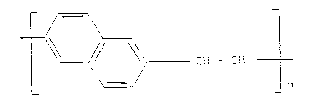


These alternative ring systems may also carry one or more substituents of the type described above in relation to the phenylene ring. - (ii) replacing the phenylene ring with a heterocyclic ring system such as a furan ring to give structures such as:-

As before, the furan ring may carry one or more substituents of the type described above in relation to phenylene rings. - (iii) increasing the number of vinylene moieties associated with each phenylene ring (or each of the other alternative ring systems described above in (i) and (ii)) to give structures such as:-


- Once again, the ring systems may carry the various substituents described above.
- These various different PPV derivatives will possess different semiconductor energy gaps; this should permit the construction of electroluminescent devices which have emission at different wavelengths covering the entire visible part of the spectrum.
- The film of conjugated polymer may be prepared by means of a chemical and/or thermal treatment of a solution - processible or melt-processible "precursor" polymer. The latter can be purified or pre-processed into the desired form before subsequent transformation to the conjugated polymer via an elimination reaction.
- Films of the various derivatives of PPV described above can be applied onto a conducting substrate in similar manner by using an appropriate sulphonium precursor.
- In certain circumstances it may be advantageous to use polymer precursors which have a higher solubility in organic solvents than the sulphonium salt precursors (III). Enhanced solubility in organic solvents can be achieved by replacing the sulphonium moiety in the precursor by a less hydrophilic group such as an alkoxy group (usually methoxy), or a pyridinium group.
- Typically, a film of poly(phenylinevinylene) is applied onto a conducting substrate by a method which relies on a reaction scheme such as is illustrated in Figure 1. The sulphonium salt monomer (II) is converted into a precursor polymer (III) in aqueous solution or in a solution of methanol/water, or methanol. Such a solution of the precursor-polymer (III) can be applied onto a conducting substrate by means of standard spin-coating techniques as used in the semiconductor industry for photoresist processing. The resultant film of precursor-polymer III can then be converted into poly(phenylene vinylene) (I) by heating to temperatures typically in the range 200-350°C.
- Details of the conditions necessary for the chemical synthesis of the monomer (II), its polymerisation to the precursor (III) and its thermal conversion to PPV are described in the literature, for example in D.D.C. Bradley, J. Phys. D (Applied Physics) 20, 1389 (1987); and J.D. Stenger Smith, R.W. Lenz and G. Wegner,
Polymer 30, 1048 (1989). - We have found that with poly(phenylenevinylene) films of a thickness in the
range 10 nm to 10 micrometres can be obtained. These PPV films are found to have very few pin holes. The PPV film has a semiconductor energy gap of about 2.5eV (500nm); it is robust, shows little reaction with oxygen at room temperature, and is stable out of air at temperatures well in excess of 300°C. - Enhanced ordering in the conjugated material may be achieved by modifying the leaving group of the precursor polymer to ensure that the elimination proceeds smoothly via a simple reaction without generation of additional intermediate structures. Thus, for example, the normal dialkyl sulphonium moiety can be replaced with a tetrahydrothiophenium moiety. The latter eliminates as a single leaving group without decompositon, as is seen for dialkyl sulphide, into an alkyl mercaptan. In the examples described here, the precursor polymers used include both that with dimethyl sulphide and tetrahydrothiophene as the leaving group. Both precursors produce film of PPV suitable for use in the device structures shown in examples below.
- A further material which may be suitable for forming the film of conjugated polymer is poly(phenylene).
- This material may be prepared by starting from biologically synthesised derivatives of 5,6-dihydroxycyclohexa-1,3-dienes. These derivatives can be polymerised by use of radical initators into a polymer precursor that is soluble in simple organic solvents. This preparation of poly(phenylene) is more fully described in Ballard et al, J. Chem. Soc. Chem. Comm. 954 (1983).
- A solution of the polymer precursor can be spin coated as a thin film onto a conducting substrate and then be converted to the conjugated poly(phenylene) polymer by a heat treatment, typically in the range 140 to 240°C.
- Copolymerisation with vinyl or diene monomers can also be performed so as to obtain phenylene copolymers.
- A further category of materials which can be used to form the required film of conjugated polymer is a conjugated polymer which is itself either solution processible or melt processible by virtue of the presence of bulky pendant side groups attached to the main conjugated chain or by virtue of the inclusion of the conjugated polymer into a copolymer structure of which one or more components are non-conjugated. Examples of the former include:-
- (a) Poly(4,4′-diphenylenediphenylvinylene) [PDPV] is an arylene vinylene polymer in which both vinylene carbons are substituted by phenyl rings. It is soluble in common organic solvents thus enabling the preparation of thin films.
- (b) Poly(1,4-phenylene-1-phenylvinylene) and poly(1,4-phenylenediphenylvinylene) polymers are analogues of PPV in which respectively one and both vinylene carbons are substituted with phenyl groups. They are both soluble in organic solvents and may be cast or spun into thin film form.
- (c) Poly(3-alkylthiophene) polymers (alkyl is one of propyl, butyl, pentyl, hexyl, heptyl, octyl, decyl, undecyl, dodecyl etc) which are solution processible in common organic solvents and which for longer alkyl sequences (alkyl greater than or equal to octyl) are also melt processible.
- (d) Poly(3-alkylpyrrole) polymers which are expected to be similar to the poly(3-alkylthiophene) polymers.
- (e) Poly(2,5-dialkoxy-p-phenylenevinylene) polymers with alkyl greater than butyl are solution processible.
- (f) Poly(phenylacetylene) is a derivative of polyacetylene in which the hydrogen atoms along the chain are replaced by phenyl groups. This substitution renders the material soluble.
- In some circumstances it may also be appropriate to form polymer blends of the conjugated polymer with other polymers so as to obtain the required processibility of the polymer and thereby facilitate forming of the required thin uniform films of the polymer on the conducting substrate (the charge injecting contact layer).
- When such copolymers or polymer blends are used to form the film of conjugated polymer, the active region of the electroluminescent device which incorporates the said film of conjugated polymer must contain a volume fraction of conjugated polymer which is greater than or equal to the percolation threshold of the copolymer or polymer blend.
- The semiconductor electroluminescent layer may be formed as a composite layer with layers of polymers with different band gaps and/or majority charge species so that, for example, concentration of the injected charge, from the charge injecting contact layer, within a particular region of the EL device may be achieved. Composite layers may be fabricated by successive deposition of polymer layers. In the case where films are deposited in the form of the precursor by spin- or draw-coating to the conjugated polymer, the conversion process to the conjugated polymer renders the film insoluble, so that subsequent layers may be similarly applied without dissolution of the previously deposited film.
- For a better understanding of the present invention, and to show how the same may be carried into effect, reference will now be made, by way of example, to the accompanying drawings in which:
- Figure 1 is a formulae drawing showing a reaction scheme for laying down the conjugated polymer;
- Figures 2 and 3 are sketches of an electroluminescent device in accordance with the present invention;
- Figure 4 is a graph of the electroluminescent output of the device described with reference to Figures 2 and 3;
- Figures 5 and 6 are graphs of current flow VS light emission, and output intensity VS applied voltage, respectively for an electroluminescent device according to another example of the invention; and
- Figures 7 and 8 are graphs respectively of the current output and electroluminescent intensity of a further example of the invention.
- Referring now to Figures 2 and 3 an EL device was constructed as follows:
- Onto the upper surface of a substrate of glass for example a silica or
borosilicate glass 1 of approximately 1mm thickness, a first charge injectingcontact layer 2 was formed. The charge injecting contact layer was formed by thermal evaporation of aluminium through a shadow-mask resulting in a layer of approximately 20 nm in thickness. The shadow-mask was used to define a pattern which was a series of parallel strips of width 2mm, separation 2mm andlength 15 mm. The resulting aluminium charge injecting contact layer was then exposed to the air to allow formation of a thinsurface oxide layer 3. This then formed the electron injecting contact layer. - A solution of the precursor to PPV, in methanol, having a concentration in the
range 1 gram polymer to 10 to 25 ml of methanol, was spin-coated onto the combination substrate described above. This was achieved by spreading the polymer solution over the whole surface of the combination substrate and then spinning the substrate, held with its upper surface horizontal, about a vertical axis at speeds of up to 5000 r.p.m. The resultant substrate and precursor polymer layer was then heated in a vacuum oven at a temperature of 300°C for 12 hours. This heat treatment converted the precursor polymer to PPV, and theresultant PPV film 4 had a thickness in the range 100 to 300 nm. The minimum requirements for the film thickness is set by the film conductance and a lower limit is in the region of 20 nm. However, the preferred range of thickness is 20 nm to 1 µm. - A second charge injecting contact layer (5) was then formed by the evaporation of gold or aluminium onto the PPV film. A shadow mask was again used to define a pattern on the surface of the PPV film so that a series of parallel strips of width 2mm, separation 2mm and
length 15 mm was formed rotated at right angles to the first charge injecting contact layer strips. The thickness of the second charge injecting contact layer was in the range 20-30nm. This then formed the hole-injecting contact layer. - It is preferable that at least one of the charge injecting contact layers is transparent or semitransparent in order to allow light emission from the EL device perpendicular to the plane of the device. This is achieved here with aluminium and gold layers of a thickness not exceeding 30 mm. For a device with the thickness of the PPV layer about 200 nm, the threshold voltage for charge injection and the appearance of strong electroluminescence is about 40 volts. The voltage gives a threshold electric field of 2 x 10⁶ Vcm⁻¹. At a current density of 2mA/cm² the light emission through the semitransparent electrodes was visible by eye under normal lighting conditions. The output of the device showed only weak dependance on frequencies up to 100 kHz. This demonstrates that the response time of the EL device is very short and is faster than 10 microseconds. When in use the EL device was operated in air with no special precautions taken and exhibited no obvious indications of degradation.
- The light output from the device was spectrally resolved with a grating monochromator and detected with a silicon photovoltaic cell, and measurements were performed both at room temperature (20°C) and also with the device held in a cryostat with optical access, at low temperatures. Results are shown in Figure 4. The EL spectrum shows light output over the spectral range 690 to 500 nm (1.8 to 2.4 eV) with peaks separated by about 0.15 eV which shift in position a little with temperature.
- Other materials which are suitable for use as an electron-injecting contact layer because they have a low work function relative to the EL layer are: n-doped silicon (amorphous or crystalline), silicon with an oxide coating, alkali and alkaline-earth metals either pure or alloyed with other metals such as Ag. Also thin layers of "n-type doped" conjugated polymers may be interposed between a metallic layer and the electroluminescent polymer layer to form the electron-injecting contact layer.
- Other materials which are suitable for use as a hole-injecting contact layer because they have a high work function relative to the EL layer are: indium/tin oxides (which are transparent in the visible part of the spectrum), platinum, nickel, palladium and graphite. Also thin layers of "p-type doped" conjugated polymers, such as electrochemically polymerised polypyrrole or polythiophene may be interposed between a metallic layer and the electroluminescent polymer layer to form the hole-injecting contact layer.
- The above mentioned materials may be applied as follows: all metals except those with very high melting point temperatures such as platinum may be deposited by evaporation; all metals including indium/tin oxide may be deposited using DC or RF sputtering and also electron beam evaporation; for amorphous silicon deposition may be done by glow-discharge deposition from mixtures of silane and dopants such as phosphine.
- The following are some examples of structures using these materials.
- The structure for this example is built up as a series of layers on a glass substrate. First, a layer of conducting but transparent indium oxide was deposited onto the substrate by a process involving ion-beam sputtering from an indium target in the presence of oxygen.
- Samples are prepared in cryopumped system with a base pressure of 10⁻⁸ mbar (1 bar = 10⁵ Pa). The substrate is water-cooled, remaining at room temperature for all depositions used here. Ion-beam sputtering from an indium target at deposition rates of typically 0.1 nm/sec, in the presence of an oxygen pressure of typically 2 x 10⁻⁴ mbar, produced films of transparent indium oxide with resistivities of typically 5 x 10⁻⁴ Ω cm. Typical thicknesses of 100 nm give specific sheet resistances of about 50Ω per square. Such films have optical transmission coefficients in the visible portion of the spectrum of better than 90%.
- These films have an amorphous structure, as determined from X-ray and electron diffraction measurements.
- A layer of PPV is next deposited onto the indium oxide layer, using the procedure described in example 1 above. A top contact of aluminium is finally deposited by evaporation, typically to a thickness of 50 nm. This structure is operated with the indium oxide contact layer functioning as the positive contact, and the aluminium contact as the negative contact. Light emission is viewed through the indium oxide layer.
- Results for a structure constructed this way, with a layer of PPV of thickness 70 nm, and an active area of 2 mm² are shown in Figures 5 and 6. The threshold for current flow associated with light emission is seen to be at about 14 V in Figure 5. The variation in the intensity of the spectrally-integrated light output for the device is shown as a function of current in Figure 6.
- The fabrication of this structure is as for Example 2 above up to the top metal contact. Here, we deposit by evaporation an alloy of silver and magnesium to form the top contact which acts as the negative contact. The evaporation is performed by heating a mixture of silver and magnesium powders in a molar ration of 1 to 10 in a boat, and film thicknesses of typically 50 nm were deposited.
- Magnesium is desirable as a material for the negative electrode as it has a low work function. The addition of silver to form an alloy improves the adhesion of the metal film to the polymer layer, and improves its resistance to oxidation. The current/voltage and EL properties of these samples were similar to those described in Example 2.
- These structures were fabricated with a layer of amorphous silicon-hydrogen alloy acting as the negative electrode, and indium oxide as the positive electrode. A glass substrate is used with an evaporated Metal contact layer of aluminium or chromium. The amorphous silicon-hydrogen film was then deposited by radio-frequency, RF, sputtering as detailed below.
- The RF sputterer used has two targets, a liquid Nitrogen cooled getter and is operated with a target-substrate separation of 8 cm. The chamber has a base pressure of 5 x 10⁻⁸ mbar. Magnetron targets are loaded with layers of n-doped Si wafers to a thickness of 3 mm. The targets are cleaned by presputtering for 1-2 hours prior to sample deposition. Substrates prepared as above are radiatively heated so that the temperature at the back side of the 3 cm thick Cu and Al substrate plate is at 250-300 °C. Substrates are rotated at about 6 revs/min. The sputtering gas used is 30% H₂ in Ar, at a pressure of 0.007-0.013 mbar, and is continually passed through the chamber during deposition. The RF power used is 250W with a reflected power of 2W. Deposition rates are typically 12nm/min giving deposition times of 1.5 hours for film thicknesses of 1 µm.
- The resulting amorphous Si is reddish brown in colour and has a d.c. resistivity of between 5 x 10⁶ and 5 x 10⁸ Ωcm. [This found by evaporating two Al pads, either above or below the sample, of
length 3 mm and with a separation of 0.25 mm and measuring the resistance between these two contacts]. - A layer of PPV was then applied to the amorphous silicon-hydrogen layer, as described in Example 1 above, and this was followed with a layer of indium oxide, deposited directly onto the PPV layer, using the procedure described in Example 2.
- Results obtained for a structure fabricated using the steps outlined above are shown in Figures 7 and 8 for a structure of
area 14 mm², and layer thicknesses of 1 µm for the silicon-hydrogen, 40 nm for the PPV and 250 nm for the indium oxide. Figure 7 shows the current versus voltage characteristic for the device in forward bias (indium oxide positive), and Figure 8 shows the variation in integrated light output with current. The onset of charge injection and light emission is at about 17 V, and the rise in current above this threshold is, due to the presence here of the resistive silicon-hydrogen layer, more gradual than observed in structures without it, as seen for example in Figure 5. - Structures of this type did also show weaker EL in reverse bias (indium oxide contact negative with respect to the silicon-hydrogen contact). The preferred mode of operation, however, is in forward bias.
- Fabrication as in example 4, but with the top layer of indium oxide replaced by a layer of semitransparent gold or aluminium. Structures fabricated with the top layer of thickness about 20 nm showed EL through this top contact. These devices showed similar characteristics to the examples discussed above.
- The method of fabrication of Example 4 could also be used with the contact layers described in Examples 2 and 3.
- There are other methods, known per se, for depositing silicon/hydrogen layers and indium oxide layers. For silicon this could include glow discharge of silane and evaporation. For indium oxide other possibilities include tin with the indium, to form indium tin oxide (ITO), which has very similar electrical properties to the indium oxide that we have used here. Deposition methods include evaporation, RF and DC sputtering.
- The choice of thickness for the charge injecting contact layers will be determined by the deposition technique used and also the desired optical transparency of the contact layer. The ease of charge injection may be improved by constructing the charge injecting contact layers as composites. Such composites would incorporate thin layers of oxidised and reduced conjugated polymers for hole and electron injection respectively. These extra layers of conjugated polymer may or may not be the same as the active electroluminescent polymer layer. Methods of doping such materials are well known in the field and are clearly described in "Handbook of Conducting Polymers" T.J. Skotheim.
- Although in certain circumstances it is preferable that at least one of the charge injecting contact layers is transparent or semitransparent in order to allow emission of radiation perpendicular to the plane of the device it is not necessarily the case for example when emission within the plane of the device only is required.
- The limit to the size of the EL device produced is determined by the size of the substrate which can be used for spin-coating. For example, 15 cm diameter silicon wafers have been coated in this way. To coat much larger areas, techniques such as draw-coating may be used instead. It is therefore feasible that EL devices using conjugated polymers with areas of square metres may be constructed.
- At least some of the conjugated polymers, including PPV, are capable of withstanding post-processing such as the deposition of metal layers in which the deposition is required to be at very high temperatures for evaporation, or the deposition of amorphous silicon layers, followed by photolithographic processes for the definition of active electroluminescent areas. Although it is preferable, with the use of PPV, for either spin- or draw-coating to be used as the methods for applying the precursor polymer to the substrate depending upon the conjugated polymer and the type of EL device required spin-, draw-coating and melt-processing are all methods which may be used to deposit the conjugated polymer onto the substrate.
- The EL device may be used in a variety of ways where electroluminescence is of use. It may be used where semiconductor LED's have traditionally been used. It may also be used where traditionally liquid crystals have been used, the EL device having many properties which make it a desirable alternative to liquid crystals.
- Since the EL device is light-emitting in contrast to liquid crystal displays, the viewing angle is wide. Furthermore, large area EL devices can be achieved where problems associated with substrate flatness and spacing have been encountered with large area liquid crystal displays. The EL devices are particularly suitable for matrix-addressed displays for example televisions and computer displays. An example of electroluminescent devices for use in a matrix-addressed displays is shown in Figure 3 where the charge injecting contact layers are applied in strips, either side of the semiconductor layer, the strips of one contact layer being orthogonal to the strips of the other contact layer. The matrix-addressing of individual EL devices or areas of the semiconductor layer called pixels of the display is achieved by the selection of a particular strip in the lower charge injecting contact layer and a particular strip, at right angles to the first strip, in the upper charge injecting contact layer. Furthermore since the EL device has such a high speed of response then the EL device is suitable for use as a television screen, particularly since the colour of the emitted light may be controlled through the choice of the conjugated polymer and so its semiconductor band gap and so colour displays using green, red and blue pixels, suitable for colour mixing, are possible through the location of different conjugated polymers in the EL device.
- EL devices may also be used as individual shaped elements for indicators in vehicle dashboards, on cookers or video recorders for example. Each element may be produced in the required shape for the intended application. Furthermore the EL device need not be flat and could, for example, be formed after fabrication, to follow contours in three dimensions for example the contours of a windscreen in a vehicle or aircraft. For such use the precursor polymer would have to be applied to a suitable substrate such as transparent polymer film such as polyester, polyvinylidene fluoride or polyimide. If the precursor polymer is applied to such flexible polymer films then continuous fabrication of the EL device, onto a roll, is possible. Alternatively the precursor polymer may be applied, using for example a draw-coating process, onto a pre-fabricated contoured substrate.
- Finally use of the EL devices is envisaged in optical communications where the EL device may be fabricated directly onto a prepared structure to act as a light source with efficient optical coupling of the EL device with optical fibres and/or thin-film waveguides. A similar application is described in an article by Satoshi Ishihara in Science and Technology in Japan of July 1989,
pages 8 to 14 entitled "Optical Information Processing". - EL device light sources may be suitable for use as lasers.
Claims (26)
- An electroluminescent device comprising:
a light emissive layer (4) in the form of a thin dense polymer film comprising at least one polymer;
a first contact layer (2) arranged on one side of the light emissive layer selected so that on application of an electric field to said device charge carriers of a first type are injected into the light emissive layer; and
a second contact layer (5) arranged on the other side of the light emissive layer characterised in that the second contact layer is selected so that on application of an electric field to said device charge carriers of a second type are injected into the light emissive layer; and
the light emissive layer comprising a semiconductive conjugated polymer present in a volume fraction which allows the percolation threshold for charge transport of the polymer film to be achieved, said semiconductive conjugated polymer having a sufficiently low concentration of extrinsic charge carriers that on applying an electric field between the first and second contact layers across the light emissive layer so as to render the second contact layer positive relative to the first contact layer charge carriers of said first and second types are injected into the light emissive layer and combine to form charge carrier pairs in the semiconductive conjugated polymer which pairs decay radiatively so that radiation is emitted from said conjugated polymer. - An electroluminescent device as claimed in claim 1, wherein the conjugated polymer is poly(p-phenylenevinylene) [PPV] of formula

- An electroluminescent device as claimed in either of claims 1 or 2, wherein the thin dense polymer film is of substantially uniform thickness in the range 10nm to 5µm.
- An electroluminescent device as claimed in any of the preceding claims, wherein the conjugated polymer has a semiconductor band gap in the range 1eV to 3.5eV.
- An electroluminescent device as claimed in any of the preceding claims, wherein the first charge injecting contact layer is a thin layer of aluminium (2) one surface having formed a thin oxide layer (3), the first surface of the semiconductor layer (4) being in contact with the said oxide layer.
- An electroluminescent device as claimed in any of claims 1 to 4 wherein the first contact layer is selected from the group comprising aluminium or an alloy of magnesium and silver.
- An electroluminescent device as claimed in claim 5, wherein the second charge injecting contact layer (5) is selected from the group comprising aluminium and gold.
- An electroluminescent device as claimed in any of the preceding claims, wherein at least one of the first and second charge injecting contact layers is at least semi-transparent.
- An electroluminescent device as claimed in claim 6, wherein the second contact layer (5) comprises indium oxide or indium tin oxide.
- An electroluminescent device as claimed in any of claims 1 to 4, wherein the first contact layer comprises amorphous silicon and the second contact layer is selected from the group comprising aluminium, gold and indium oxide.
- An electroluminescent device as claimed in any of the preceding claims, wherein at least one of the first and second charge injecting contact layers is also in contact with a supporting substrate.
- An electroluminescent device as claimed in claim 11, wherein the supporting substrate is silica glass.
- An electroluminescent device as claimed in claim 11 or 12 wherein the supporting substrate is a flexible transparent polymer.
- An array of electroluminescent devices, each electroluminescent device as claimed in any of the preceding claims, said first and second charge injecting contact layers being arranged to permit selective addressing in said array.
- A method of manufacture of an electroluminescent device according to claim 1 comprising providing a layer of a light emissive polymer between first and second contact layers, wherein the first contact layer is selected so that an application of an electric field to said device charge carriers of a first type are injected into the light emissive layer, characterised by the steps of:a) depositing onto a substrate one of said first and second contact layers;b) depositing on said contact layer a layer of a precursor polymer as a polymer film and then heating the deposited precursor polymer to a high temperature to form the light emissive layer as a semiconductive conjugated polymer; andc) providing the other one of said first and second contact layers, the second contact layer being selected and arranged so that on application of an electric field to said device charge carriers of a second type are injected into the light emissive layer, wherein the semiconductive conjugated polymer has a sufficiently low concentration of extrinsic charge carriers that on applying an electric field between the first and second contact layers across a semiconductor layer so as to render the second contact layer positive relative to the first contact layer charge carriers of said first and second types are injected into the semiconductor layer and combine to form in the conjugated polymer charge carrier pairs which decay radiatively so that radiation is emitted from the conjugated polymer.
- A method as claimed in claim 15, comprising the steps of firstly depositing the first charge injecting contact layer onto the substrate to form a composite substrate before the step of depositing the precursor polymer as a thin dense polymer film onto the first charge injecting contact layer.
- A method as claimed in either of claims 15 or 16, wherein the precursor polymer is soluble and is deposited as a thin polymer film on the substrate by spin-coating.
- A method as claimed in any of claims 15 to 17, wherein the precursor polymer is a precursor polymer for poly (p-phenylenevinylene) [PPV].
- A method as claimed in any of claims 15 to 18, wherein the thin dense polymer film is of uniform thickness in the range 10nm to 5um.
- A method as claimed in any of claims 15 to 19, wherein the first charge injecting contact layer is a thin layer of aluminium one surface having formed a thin oxide layer, the thin oxide layer of the first charge injecting contact layer being placed in contact with the semiconductor layer.
- A method as claimed in any of claims 15 to 20, wherein the second charge injecting contact layer is selected from the group comprising aluminium and gold.
- A method as claimed in any of claims 16 to 19, wherein the first contact layer is selected from the group comprising aluminium and magnesium/silver alloy and the second contact layer is indium oxide.
- A method as claimed in any of claims 15 to 19 wherein the first contact layer comprises amorphous silicon and the second contact layer is selected from the group comprising aluminium, gold and indium oxide.
- A method as claimed in any of claims 15 to 23, wherein the first and second charge injecting contact layers are deposited by evaporation.
- A method as claimed in any of claims 15 to 23, wherein the supporting substrate is silica glass.
- A method as claimed in any of claims 15 to 24 wherein the supporting substrate is a flexible transparent polymer.
Applications Claiming Priority (3)
| Application Number | Priority Date | Filing Date | Title |
|---|---|---|---|
| GB8909011 | 1989-04-20 | ||
| GB898909011A GB8909011D0 (en) | 1989-04-20 | 1989-04-20 | Electroluminescent devices |
| PCT/GB1990/000584 WO1990013148A1 (en) | 1989-04-20 | 1990-04-18 | Electroluminescent devices |
Publications (2)
| Publication Number | Publication Date |
|---|---|
| EP0423283A1 EP0423283A1 (en) | 1991-04-24 |
| EP0423283B1 true EP0423283B1 (en) | 1995-01-25 |
Family
ID=10655404
Family Applications (1)
| Application Number | Title | Priority Date | Filing Date |
|---|---|---|---|
| EP90906272A Expired - Lifetime EP0423283B1 (en) | 1989-04-20 | 1990-04-18 | Electroluminescent devices |
Country Status (14)
| Country | Link |
|---|---|
| US (2) | US5247190A (en) |
| EP (1) | EP0423283B1 (en) |
| JP (3) | JP3249971B2 (en) |
| KR (1) | KR100189398B1 (en) |
| AT (1) | ATE117834T1 (en) |
| AU (1) | AU626415B2 (en) |
| BR (1) | BR9006718A (en) |
| CA (1) | CA2030785C (en) |
| DE (1) | DE69016345T2 (en) |
| ES (1) | ES2070320T3 (en) |
| FI (1) | FI112555B (en) |
| GB (1) | GB8909011D0 (en) |
| HK (1) | HK24597A (en) |
| WO (1) | WO1990013148A1 (en) |
Cited By (10)
| Publication number | Priority date | Publication date | Assignee | Title |
|---|---|---|---|---|
| US5869350A (en) * | 1991-02-27 | 1999-02-09 | The Regents Of The University Of California | Fabrication of visible light emitting diodes soluble semiconducting polymers |
| US6249085B1 (en) | 1999-03-17 | 2001-06-19 | Tdk Corporation | Organic electroluminescent device with a high-resistance inorganic hole injecting and transporting layer |
| US6288487B1 (en) | 1999-03-17 | 2001-09-11 | Tdk Corporation | Organic electroluminescent device with a high-resistance inorganic electron injecting and transporting layer |
| US6369507B1 (en) | 1999-06-07 | 2002-04-09 | Tdk Corporation | Organic EL display apparatus with a switching device |
| US6404126B1 (en) | 1998-11-25 | 2002-06-11 | Tdk Corporation | Organic electroluminescent device having a conjugated polymer and an inorganic insulative electron injecting and transporting layer |
| US6458909B1 (en) | 1996-12-16 | 2002-10-01 | Hoechst Aktiengesellschaft | Aryl-substituted poly (p-arylene-vinylenes), process for their preparation and their use in electroluminescence components |
| DE10059810C2 (en) * | 2000-12-01 | 2003-12-11 | Fraunhofer Ges Forschung | Broadband light-emitting polymeric diodes (PLED) and processes for their production |
| US6667729B2 (en) | 2000-09-01 | 2003-12-23 | Samsung Sdi Co., Ltd. | Method of electrically addressing polymer fluorescent display element and polymer fluorescent display element |
| WO2022003353A1 (en) | 2020-07-01 | 2022-01-06 | Peroled Limited | Improved light emitting devices |
| WO2022003352A1 (en) | 2020-07-01 | 2022-01-06 | Peroled Limited | Novel light emitting device architectures |
Families Citing this family (1862)
| Publication number | Priority date | Publication date | Assignee | Title |
|---|---|---|---|---|
| US5015544A (en) | 1989-02-08 | 1991-05-14 | Strategic Energy Ltd. | Battery with strength indicator |
| EP0443861B2 (en) * | 1990-02-23 | 2008-05-28 | Sumitomo Chemical Company, Limited | Organic electroluminescence device |
| GB9018698D0 (en) * | 1990-08-24 | 1990-10-10 | Lynxvale Ltd | Semiconductive copolymers for use in electroluminescent devices |
| US5389444A (en) * | 1991-09-18 | 1995-02-14 | Idemitsu Kosan Co., Ltd. | Organic electroluminescence device |
| GB9201240D0 (en) * | 1992-01-21 | 1992-03-11 | Lynxvale Ltd | Conjugated polymer |
| GB9215928D0 (en) * | 1992-07-27 | 1992-09-09 | Cambridge Display Tech Ltd | Manufacture of electroluminescent devices |
| GB9215929D0 (en) * | 1992-07-27 | 1992-09-09 | Cambridge Display Tech Ltd | Electroluminescent devices |
| JP3300069B2 (en) * | 1992-11-19 | 2002-07-08 | パイオニア株式会社 | Organic electroluminescence device |
| GB9226475D0 (en) * | 1992-12-18 | 1993-02-10 | Cambridge Display Tech Ltd | Chromophoric polymeric compositions |
| US5334539A (en) * | 1993-01-29 | 1994-08-02 | Iowa State University Research Foundation, Inc. | Fabrication of poly(p-phenyleneacetylene) light-emitting diodes |
| US5352906A (en) * | 1993-01-29 | 1994-10-04 | Iowa State University Research Foundation, Inc. | Poly (p-phenyleneneacetylene) light-emitting diodes |
| US5414069A (en) * | 1993-02-01 | 1995-05-09 | Polaroid Corporation | Electroluminescent polymers, processes for their use, and electroluminescent devices containing these polymers |
| US5376456A (en) * | 1993-05-13 | 1994-12-27 | Polaroid Corporation | Electroluminescent devices comprising polymers, and processes for their use |
| US5366559A (en) * | 1993-05-27 | 1994-11-22 | Research Triangle Institute | Method for protecting a substrate surface from contamination using the photophoretic effect |
| US5514878A (en) * | 1994-03-18 | 1996-05-07 | Holmes; Andrew B. | Polymers for electroluminescent devices |
| DE69427909T2 (en) * | 1993-06-10 | 2002-04-04 | Cambridge Display Tech Ltd | POLYMERS FOR OPTICAL DEVICES |
| WO1995001871A1 (en) * | 1993-07-09 | 1995-01-19 | The Regents Of The University Of California | Electroluminescent diodes utilizing blends of polymers |
| US5589320A (en) * | 1993-07-21 | 1996-12-31 | Sumitomo Chemical Company, Limited | Polymeric fluorescent substance and organic electroluminescence devices using the same |
| DE4325885A1 (en) * | 1993-08-02 | 1995-02-09 | Basf Ag | Electroluminescent arrangement |
| US5965241A (en) * | 1993-08-25 | 1999-10-12 | Polaroid Corp | Electroluminescent devices and processes using polythiophenes |
| GB9317932D0 (en) * | 1993-08-26 | 1993-10-13 | Cambridge Display Tech Ltd | Electroluminescent devices |
| JP3534445B2 (en) * | 1993-09-09 | 2004-06-07 | 隆一 山本 | EL device using polythiophene |
| DE69433830T2 (en) * | 1993-09-14 | 2005-06-16 | Covion Organic Semiconductors Gmbh | Process for the preparation of polymers of alpha-omega-unsaturated compounds and the resulting high molecular weight conjugated polymers |
| DE4331401A1 (en) * | 1993-09-15 | 1995-03-16 | Hoechst Ag | Use of polymers with isolated chromophores as electroluminescent materials |
| US5700696A (en) * | 1993-11-08 | 1997-12-23 | Lucent Technologies Inc. | Method for preparation of conjugated arylene or heteroarylene vinylene polymer and device including same |
| US5504323A (en) * | 1993-12-07 | 1996-04-02 | The Regents Of The University Of California | Dual function conducting polymer diodes |
| US5478665A (en) * | 1994-02-02 | 1995-12-26 | Strategic Electronics | Battery with strength indicator |
| US5759709A (en) * | 1994-03-10 | 1998-06-02 | Sumitomo Chemical Company, Limited | Polymeric fluorescent substance and organic electroluminescence device |
| US5682043A (en) * | 1994-06-28 | 1997-10-28 | Uniax Corporation | Electrochemical light-emitting devices |
| DE4422670A1 (en) * | 1994-06-30 | 1996-01-04 | Hoechst Ag | Conjugated polymers with partial structures and their use as electroluminescent materials |
| DE4423098A1 (en) | 1994-07-01 | 1996-01-04 | Hoechst Ag | Use of conjugated compounds containing pyrimidine groups as electroluminescent materials |
| US5558904A (en) * | 1994-07-08 | 1996-09-24 | Xerox Corporation | Electroluminescent devices containing a conjugated polymer obtained via halogen precursor route chemistry |
| DE69514495T2 (en) * | 1994-08-11 | 2000-08-10 | Koninkl Philips Electronics Nv | SOLID STATE IMAGE AMPLIFIER AND X-RAY EXAMINER WITH A SOLID STATE IMAGE AMPLIFIER |
| DE4431039A1 (en) * | 1994-09-01 | 1996-03-07 | Hoechst Ag | Poly (4,5,9,10-tetrahydropyrene-2,7-diyl) derivatives and their use as electroluminescent materials |
| DE69529512T2 (en) * | 1994-09-06 | 2003-11-13 | Koninkl Philips Electronics Nv | Electroluminescent device with a poly-3,4-ethylene-dioxythiophene layer |
| US5523555A (en) * | 1994-09-14 | 1996-06-04 | Cambridge Display Technology | Photodetector device having a semiconductive conjugated polymer |
| US5674635A (en) * | 1994-09-28 | 1997-10-07 | Xerox Corporation | Electroluminescent device |
| DE59504835D1 (en) * | 1994-09-30 | 1999-02-25 | Hoechst Ag | NITROGEN POLYMERS AS ELECTROLUMINESCENT MATERIALS |
| DE69514604T2 (en) * | 1994-10-04 | 2000-06-21 | Aventis Res & Tech Gmbh & Co | Process for the preparation of polymers from alpha, omega unsaturated conjugated compounds |
| US5560957A (en) * | 1994-10-28 | 1996-10-01 | Xerox Corporation | Electroluminescent device |
| US6063642A (en) * | 1994-11-15 | 2000-05-16 | Peter S. Zory | Method for generating luminescence from a buried layer in a multilayer compound semiconductor material using a liquid contact |
| GB9423692D0 (en) * | 1994-11-23 | 1995-01-11 | Philips Electronics Uk Ltd | A photoresponsive device |
| FR2727598A1 (en) * | 1994-11-24 | 1996-05-31 | Magneti Marelli France | Motor vehicle instrument panel light source |
| DE4442050A1 (en) | 1994-11-25 | 1996-05-30 | Hoechst Ag | Heterospiro compounds and their use as electroluminescent materials |
| DE4442052A1 (en) * | 1994-11-25 | 1996-05-30 | Hoechst Ag | Conjugated polymers with hetero-spiroatoms and their use as electroluminescent materials |
| US5574291A (en) * | 1994-12-09 | 1996-11-12 | Lucent Technologies Inc. | Article comprising a thin film transistor with low conductivity organic layer |
| US5703436A (en) * | 1994-12-13 | 1997-12-30 | The Trustees Of Princeton University | Transparent contacts for organic devices |
| US6559256B2 (en) | 1994-12-28 | 2003-05-06 | Cambridge Display Technology Ltd. | Polymers for use in optical devices |
| US5609970A (en) * | 1995-01-12 | 1997-03-11 | Polaroid Corporation | Electroluminescent device with polymeric charge injection layer |
| DE19500912A1 (en) * | 1995-01-13 | 1996-07-18 | Basf Ag | Electroluminescent arrangement |
| TW334474B (en) * | 1995-02-01 | 1998-06-21 | Sumitomo Kagaku Kk | Method for making a polymeric fluorescent substrate and organic electrolumninescent element |
| DE19505942A1 (en) | 1995-02-21 | 1996-08-22 | Bayer Ag | (Co) polymers based on vinyl units and their use in electroluminescent arrangements |
| US5693962A (en) * | 1995-03-22 | 1997-12-02 | Motorola | Full color organic light emitting diode array |
| US5587589A (en) * | 1995-03-22 | 1996-12-24 | Motorola | Two dimensional organic light emitting diode array for high density information image manifestation apparatus |
| DE19511484A1 (en) * | 1995-03-29 | 1996-10-02 | Bayer Ag | (Co) polymers based on vinyl units and their use in electroluminescent arrangements |
| US6075106A (en) * | 1995-03-29 | 2000-06-13 | D-51368 Bayer Ag | (Co)polymers based on vinyl units and use thereof in electroluminescent devices |
| GB2314196B (en) * | 1995-04-18 | 1998-06-17 | Cambridge Display Tech Ltd | A display |
| WO1996033593A1 (en) * | 1995-04-18 | 1996-10-24 | Cambridge Display Technology Limited | Manufacture of organic light emitting devices |
| GB9507862D0 (en) * | 1995-04-18 | 1995-05-31 | Cambridge Display Tech Ltd | Fabrication of organic light-emitting devices |
| WO1996033483A1 (en) * | 1995-04-18 | 1996-10-24 | Cambridge Display Technology Limited | A display |
| US5677546A (en) * | 1995-05-19 | 1997-10-14 | Uniax Corporation | Polymer light-emitting electrochemical cells in surface cell configuration |
| US5895717A (en) * | 1995-11-08 | 1999-04-20 | Uniax Corporation | Electrochemical light-emitting devices |
| WO1996036959A2 (en) * | 1995-05-19 | 1996-11-21 | Philips Electronics N.V. | Display device |
| DE69608446T3 (en) | 1995-07-28 | 2010-03-11 | Sumitomo Chemical Company, Ltd. | 2.7 ARYL 9 SUBSTITUTED FLUORESE AND 9 SUBSTITUTED FLUORESOLIGOMERS AND POLYMERS |
| IT1280453B1 (en) * | 1995-07-28 | 1998-01-20 | Carello Spa | HEADLIGHT FOR REDUCED THICKNESS VEHICLES. |
| US5708130A (en) | 1995-07-28 | 1998-01-13 | The Dow Chemical Company | 2,7-aryl-9-substituted fluorenes and 9-substituted fluorene oligomers and polymers |
| KR0155863B1 (en) * | 1995-07-31 | 1998-11-16 | 김광호 | Blue luminescent polymer and luminescent diode using the same |
| EP0784659B1 (en) * | 1995-08-03 | 1999-12-08 | Koninklijke Philips Electronics N.V. | Electroluminescent device |
| JP2002515078A (en) * | 1995-09-04 | 2002-05-21 | ヘキスト・リサーチ・アンド・テクノロジー・ドイチュラント・ゲーエムベーハー・ウント・コンパニー・カーゲー | Polymers containing triarylamine units as electroluminescent substances |
| DE19536843A1 (en) * | 1995-10-02 | 1997-04-03 | Bayer Ag | (Co) polymers based on vinyl units and their use in electroluminescent arrangements |
| US5763636A (en) * | 1995-10-12 | 1998-06-09 | Hoechst Aktiengesellschaft | Polymers containing spiro atoms and methods of using the same as electroluminescence materials |
| DE19543205A1 (en) * | 1995-11-20 | 1997-05-22 | Bayer Ag | Interlayer in electroluminescent arrangements containing finely divided inorganic particles |
| EA001312B1 (en) | 1995-12-01 | 2001-02-26 | Вантико Аг | Poly(9.9<'>-spiro-bisfuoroenes), the productionand use of same |
| JP3856504B2 (en) * | 1996-02-21 | 2006-12-13 | 独立行政法人理化学研究所 | Ultraviolet region electroluminescence device, laser light emitting device, and method for manufacturing the same |
| DE19606511A1 (en) | 1996-02-22 | 1997-09-04 | Hoechst Ag | Partially conjugated polymers with spirocenters and their use as electroluminescent materials |
| US5929194A (en) * | 1996-02-23 | 1999-07-27 | The Dow Chemical Company | Crosslinkable or chain extendable polyarylpolyamines and films thereof |
| JP3399216B2 (en) * | 1996-03-14 | 2003-04-21 | ソニー株式会社 | Semiconductor light emitting device |
| EP0891686B1 (en) | 1996-04-03 | 1999-10-06 | Ecole Polytechnique Féderale de Lausanne (EPFL) | Electroluminescent device |
| US6211613B1 (en) | 1996-04-10 | 2001-04-03 | Cambridge Display Technology Limited | High contrast electroluminescent displays |
| KR100447449B1 (en) | 1996-04-10 | 2005-01-24 | 캠브리지 디스플레이 테크놀로지 리미티드 | Organic light emitting diode colour display |
| DE19615128A1 (en) * | 1996-04-17 | 1997-10-30 | Hoechst Ag | Conjugated polymers with hetero-spiroatoms and their use as electroluminescent materials |
| JP3537591B2 (en) * | 1996-04-26 | 2004-06-14 | パイオニア株式会社 | Manufacturing method of organic EL display |
| GB9609282D0 (en) | 1996-05-03 | 1996-07-10 | Cambridge Display Tech Ltd | Protective thin oxide layer |
| DE19627071A1 (en) | 1996-07-05 | 1998-01-08 | Bayer Ag | Electroluminescent devices |
| DE19627070A1 (en) | 1996-07-05 | 1998-01-08 | Bayer Ag | Electroluminescent devices using glare systems |
| DE19628119A1 (en) * | 1996-07-12 | 1998-01-29 | Univ Bayreuth Vertreten Durch | Light-emitting apparatus |
| DE19628719B4 (en) * | 1996-07-17 | 2006-10-05 | Hans-Werner Prof. Dr. Schmidt | Electron-conducting layer in organic, electroluminescent arrangements |
| GB2315594B (en) * | 1996-07-22 | 2000-08-16 | Cambridge Display Tech Ltd | Sensing device |
| US6605823B1 (en) * | 1996-07-29 | 2003-08-12 | Cambridge Display Technology Ltd. | Electroluminescent devices with electrode protection |
| US6004681A (en) * | 1996-08-02 | 1999-12-21 | The Ohio State University Research Foundation | Light-emitting devices containing network electrode polymers in electron blocking layer |
| US5955834A (en) * | 1996-08-02 | 1999-09-21 | The Ohio State University | Light emitting devices utilizing high work function electrodes |
| US6623870B1 (en) * | 1996-08-02 | 2003-09-23 | The Ohio State University | Electroluminescence in light emitting polymers featuring deaggregated polymers |
| DE19632949A1 (en) * | 1996-08-16 | 1998-02-19 | Bayer Ag | (Co) polymers based on vinyl units and their use in electroluminescent arrangements |
| US6207301B1 (en) | 1996-08-21 | 2001-03-27 | Sumitomo Chemical Company, Limited | Polymer fluorescent substance and organic electroluminescence device |
| ATE247372T1 (en) | 1996-09-04 | 2003-08-15 | Cambridge Display Tech Ltd | LIGHT EMITTING ORGANIC DEVICES WITH IMPROVED CATHODE |
| EP0946993B8 (en) | 1996-09-04 | 2007-09-12 | Cambridge Display Technology Limited | Electrode deposition for organic light-emitting devices |
| JP3304787B2 (en) * | 1996-09-08 | 2002-07-22 | 豊田合成株式会社 | Semiconductor light emitting device and method of manufacturing the same |
| CN100485904C (en) * | 1996-09-19 | 2009-05-06 | 精工爱普生株式会社 | Matrix type display device and manufacturing method thereof |
| US20020075422A1 (en) * | 1996-09-19 | 2002-06-20 | Seiko Epson Corporation | Matrix type display device and manufacturing method thereof |
| DE19646119A1 (en) * | 1996-11-08 | 1998-05-14 | Hoechst Ag | Electroluminescent device |
| US5817430A (en) * | 1996-11-13 | 1998-10-06 | Xerox Corporation | Electroluminescent polymer compositions and processes thereof |
| US5753757A (en) * | 1996-11-13 | 1998-05-19 | Xerox Corporation | Electroluminescent polymer compositions and processes thereof |
| JP3899566B2 (en) | 1996-11-25 | 2007-03-28 | セイコーエプソン株式会社 | Manufacturing method of organic EL display device |
| GB9624706D0 (en) * | 1996-11-28 | 1997-01-15 | Cambridge Display Tech Ltd | Light emitting polymer device |
| DE19651439A1 (en) * | 1996-12-11 | 1998-06-18 | Hoechst Ag | Polymerizable biaryls, process for their preparation and their use |
| DE29621619U1 (en) | 1996-12-12 | 1997-02-27 | Siemens Ag | Device for illuminating theater stages, TV studios or the like. |
| US5966393A (en) * | 1996-12-13 | 1999-10-12 | The Regents Of The University Of California | Hybrid light-emitting sources for efficient and cost effective white lighting and for full-color applications |
| GB9701680D0 (en) * | 1997-01-28 | 1997-03-19 | Cambridge Display Tech Ltd | Viscosity modification of precursor solutions |
| JP2845233B2 (en) * | 1997-01-29 | 1999-01-13 | 双葉電子工業株式会社 | Organic electroluminescence device and method of manufacturing the same |
| US5965281A (en) * | 1997-02-04 | 1999-10-12 | Uniax Corporation | Electrically active polymer compositions and their use in efficient, low operating voltage, polymer light-emitting diodes with air-stable cathodes |
| US5958573A (en) * | 1997-02-10 | 1999-09-28 | Quantum Energy Technologies | Electroluminescent device having a structured particle electron conductor |
| DE19707452C2 (en) * | 1997-02-25 | 1999-09-02 | Bosch Gmbh Robert | Organic electroluminescent device using stable, metallic cathodes |
| US5952778A (en) * | 1997-03-18 | 1999-09-14 | International Business Machines Corporation | Encapsulated organic light emitting device |
| DE19715048C2 (en) * | 1997-04-11 | 1999-08-19 | Bosch Gmbh Robert | Process for structuring a transparent, electrically conductive layer |
| AU7251898A (en) * | 1997-04-17 | 1998-11-11 | California Institute Of Technology | Substituted poly(phenylenevinylene)s and poly(napthalenevinylene)s |
| US6309763B1 (en) | 1997-05-21 | 2001-10-30 | The Dow Chemical Company | Fluorene-containing polymers and electroluminescent devices therefrom |
| US6452218B1 (en) | 1997-06-10 | 2002-09-17 | Uniax Corporation | Ultra-thin alkaline earth metals as stable electron-injecting electrodes for polymer light emitting diodes |
| US6023259A (en) * | 1997-07-11 | 2000-02-08 | Fed Corporation | OLED active matrix using a single transistor current mode pixel design |
| US6843937B1 (en) * | 1997-07-16 | 2005-01-18 | Seiko Epson Corporation | Composition for an organic EL element and method of manufacturing the organic EL element |
| GB2328212B (en) * | 1997-08-12 | 2000-11-29 | Samsung Display Devices Co Ltd | Organic electroluminescent polymer for light emitting diode |
| GB9718393D0 (en) | 1997-08-29 | 1997-11-05 | Cambridge Display Tech Ltd | Electroluminescent Device |
| GB9718516D0 (en) | 1997-09-01 | 1997-11-05 | Cambridge Display Tech Ltd | Methods of Increasing the Efficiency of Organic Electroluminescent Devices |
| US6403236B1 (en) * | 1997-09-04 | 2002-06-11 | Sumitomo Chemical Company, Limited | Polymer light emitting device |
| EP0963686B1 (en) * | 1997-09-24 | 2001-12-12 | Koninklijke Philips Electronics N.V. | Organic electroluminescent device |
| KR100254536B1 (en) * | 1997-09-29 | 2000-05-01 | 정선종 | A EL device using a synthesis of silyl disubstituted PPV derivatives and a method of manufacturing the same |
| DE69807513T2 (en) | 1997-10-22 | 2003-04-24 | Cambridge Consultants | PORTABLE CHIP CARD |
| US5945502A (en) * | 1997-11-13 | 1999-08-31 | Xerox Corporation | Electroluminescent polymer compositions and processes thereof |
| US5879821A (en) * | 1997-11-13 | 1999-03-09 | Xerox Corporation | Electroluminescent polymer compositions and processes thereof |
| GB9724682D0 (en) | 1997-11-21 | 1998-01-21 | Cambridge Display Tech Ltd | Electroluminescent device |
| GB2331765A (en) | 1997-12-01 | 1999-06-02 | Cambridge Display Tech Ltd | Sputter deposition onto organic material using neon as the discharge gas |
| BR9906908A (en) | 1998-01-13 | 2000-10-10 | Minnesota Mining & Mfg | Gliter particles, composite article, dispersion, dispersible combination, molding compound, and injection-moldable compositions, topical medicated cosmetics and comprising gliter. |
| US6053795A (en) * | 1998-01-13 | 2000-04-25 | 3M Innovative Properties Company | Toy having image mode and changed image mode |
| US6120026A (en) * | 1998-01-13 | 2000-09-19 | 3M Innovative Properties Co. | Game with privacy material |
| DE19806037A1 (en) * | 1998-02-13 | 1999-08-19 | Aventis Res & Tech Gmbh & Co | Electroluminescent polymers and copolymers of triptycene structure |
| JP4514841B2 (en) * | 1998-02-17 | 2010-07-28 | 淳二 城戸 | Organic electroluminescent device |
| GB9803763D0 (en) | 1998-02-23 | 1998-04-15 | Cambridge Display Tech Ltd | Display devices |
| GB9803764D0 (en) | 1998-02-23 | 1998-04-15 | Cambridge Display Tech Ltd | Display devices |
| JPH11251067A (en) | 1998-03-02 | 1999-09-17 | Junji Kido | Organic electroluminescence element |
| DE19809696A1 (en) | 1998-03-06 | 1999-09-09 | Bayer Ag | Plastic substrate for solid-state lasers |
| KR100697861B1 (en) | 1998-03-13 | 2007-03-22 | 캠브리지 디스플레이 테크놀로지 리미티드 | Electroluminescent devices |
| WO1999048337A1 (en) | 1998-03-13 | 1999-09-23 | Cambridge Display Technology Ltd. | Electroluminescent devices |
| GB9805476D0 (en) | 1998-03-13 | 1998-05-13 | Cambridge Display Tech Ltd | Electroluminescent devices |
| US5962967A (en) * | 1998-03-19 | 1999-10-05 | Kiryuschev; Irina | Electroluminescent device and method of manufacturing same |
| DE19812259A1 (en) | 1998-03-20 | 1999-10-21 | Bayer Ag | EL arrangement based on tertiary amines, alcohol-soluble Alq3 derivatives or mixtures and polymeric binders |
| GB2335884A (en) | 1998-04-02 | 1999-10-06 | Cambridge Display Tech Ltd | Flexible substrates for electronic or optoelectronic devices |
| GB9808061D0 (en) | 1998-04-16 | 1998-06-17 | Cambridge Display Tech Ltd | Polymer devices |
| DE19825765A1 (en) | 1998-06-09 | 1999-12-16 | Bayer Ag | Electroluminescent devices using glare systems |
| US6403237B1 (en) | 1998-06-10 | 2002-06-11 | Sumitomo Chemical Co., Ltd. | Polymeric fluorescent substance and organic electroluminescence device |
| EP0966050A3 (en) | 1998-06-18 | 2004-11-17 | Osram Opto Semiconductors GmbH & Co. OHG | Organic light emitting diode |
| TW411726B (en) * | 1998-06-18 | 2000-11-11 | Siemens Ag | Manufacture of structurized electrodes |
| GB9813324D0 (en) * | 1998-06-19 | 1998-08-19 | Cambridge Display Tech Ltd | Light-emissive devices |
| US6615189B1 (en) * | 1998-06-22 | 2003-09-02 | Bank One, Delaware, National Association | Debit purchasing of stored value card for use by and/or delivery to others |
| US7809642B1 (en) | 1998-06-22 | 2010-10-05 | Jpmorgan Chase Bank, N.A. | Debit purchasing of stored value card for use by and/or delivery to others |
| US6127693A (en) * | 1998-07-02 | 2000-10-03 | National Science Council Of Republic Of China | Light emitting diode with blue light and red light emitting polymers |
| US6368731B2 (en) | 1998-07-04 | 2002-04-09 | Bayer Aktiengesellschaft | Electroluminescent assemblies using boron chelates of 8-aminoquinoline derivatives |
| DE19829947A1 (en) | 1998-07-04 | 2000-01-05 | Bayer Ag | Electroluminescent devices with boron chelates |
| US6316130B1 (en) | 1998-07-04 | 2001-11-13 | Bayer Aktiengesellschaft | Electroluminescent assemblies using azomethine-metal complexes |
| DE19832644C1 (en) | 1998-07-10 | 2000-04-06 | Samsung Display Devices Co Ltd | Organic light-emitting diode has light-emitting active layer of new poly(2-methoxy-5-(2'-ethylhexyloxy)-1,4-phenylene-1,2-ethenylene-2,5-dimethoxy-1,4-phenylene-1,2-ethenylene) |
| GB9815271D0 (en) | 1998-07-14 | 1998-09-09 | Cambridge Display Tech Ltd | Particles and devices comprising particles |
| JP3692844B2 (en) | 1998-07-24 | 2005-09-07 | セイコーエプソン株式会社 | Electroluminescent device and electronic device |
| US6635989B1 (en) * | 1998-08-03 | 2003-10-21 | E. I. Du Pont De Nemours And Company | Encapsulation of polymer-based solid state devices with inorganic materials |
| JP2000068065A (en) * | 1998-08-13 | 2000-03-03 | Tdk Corp | Organic el element |
| US6483099B1 (en) * | 1998-08-14 | 2002-11-19 | Dupont Displays, Inc. | Organic diodes with switchable photosensitivity |
| KR100327105B1 (en) * | 1998-08-14 | 2002-03-09 | 오길록 | High luminance-phosphor and method for fabricating the same |
| GB9818092D0 (en) | 1998-08-19 | 1998-10-14 | Cambridge Display Tech Ltd | Display devices |
| DE19839947A1 (en) | 1998-09-02 | 2000-03-09 | Bayer Ag | Electroluminescent devices with thiophene carboxylate metal complexes |
| DE19839946A1 (en) | 1998-09-02 | 2000-03-09 | Bayer Ag | Electroluminescent devices with multinuclear metal complexes |
| DE19840943A1 (en) | 1998-09-08 | 2000-03-09 | Aventis Res & Tech Gmbh & Co | Process for the preparation of derivatives of 4-alkylsulfinylmethylarylenemethanol |
| DE19841803A1 (en) | 1998-09-12 | 2000-03-16 | Bayer Ag | Organic electroluminescent device, i.e. light-emitting diode, has hole-injecting layer of polymeric organic conductor formed by coating from solution or from sub-micron dispersion |
| US6830828B2 (en) | 1998-09-14 | 2004-12-14 | The Trustees Of Princeton University | Organometallic complexes as phosphorescent emitters in organic LEDs |
| JP4138102B2 (en) * | 1998-10-13 | 2008-08-20 | セイコーエプソン株式会社 | Display device and electronic device |
| CN1191644C (en) | 1998-10-14 | 2005-03-02 | 杜邦显示器股份有限公司 | Thin meta-oxide layer as stable electron-injecting electrode for LED |
| US6274887B1 (en) | 1998-11-02 | 2001-08-14 | Semiconductor Energy Laboratory Co., Ltd. | Semiconductor device and manufacturing method therefor |
| US6617644B1 (en) | 1998-11-09 | 2003-09-09 | Semiconductor Energy Laboratory Co., Ltd. | Semiconductor device and method of manufacturing the same |
| US7141821B1 (en) | 1998-11-10 | 2006-11-28 | Semiconductor Energy Laboratory Co., Ltd. | Semiconductor device having an impurity gradient in the impurity regions and method of manufacture |
| US7022556B1 (en) | 1998-11-11 | 2006-04-04 | Semiconductor Energy Laboratory Co., Ltd. | Exposure device, exposure method and method of manufacturing semiconductor device |
| US6518594B1 (en) | 1998-11-16 | 2003-02-11 | Semiconductor Energy Laboratory Co., Ltd. | Semiconductor devices |
| US6512271B1 (en) * | 1998-11-16 | 2003-01-28 | Semiconductor Energy Laboratory Co., Ltd. | Semiconductor device |
| US6909114B1 (en) | 1998-11-17 | 2005-06-21 | Semiconductor Energy Laboratory Co., Ltd. | Semiconductor device having LDD regions |
| KR100280125B1 (en) | 1998-11-17 | 2001-02-01 | 정선종 | New blue light-emitting polymer prepared by using a new tetraphenyl derivative substituted with fluorine as a monomer and an electroluminescent device using the same |
| US6032136A (en) * | 1998-11-17 | 2000-02-29 | First Usa Bank, N.A. | Customer activated multi-value (CAM) card |
| US7660763B1 (en) | 1998-11-17 | 2010-02-09 | Jpmorgan Chase Bank, N.A. | Customer activated multi-value (CAM) card |
| US6489952B1 (en) | 1998-11-17 | 2002-12-03 | Semiconductor Energy Laboratory Co., Ltd. | Active matrix type semiconductor display device |
| US6420758B1 (en) * | 1998-11-17 | 2002-07-16 | Semiconductor Energy Laboratory Co., Ltd. | Semiconductor device having an impurity region overlapping a gate electrode |
| US6365917B1 (en) | 1998-11-25 | 2002-04-02 | Semiconductor Energy Laboratory Co., Ltd. | Semiconductor device |
| US6501098B2 (en) * | 1998-11-25 | 2002-12-31 | Semiconductor Energy Laboratory Co, Ltd. | Semiconductor device |
| US6277679B1 (en) | 1998-11-25 | 2001-08-21 | Semiconductor Energy Laboratory Co., Ltd. | Method of manufacturing thin film transistor |
| EP2264771A3 (en) | 1998-12-03 | 2015-04-29 | Semiconductor Energy Laboratory Co., Ltd. | MOS thin film transistor and method of fabricating same |
| US6420988B1 (en) | 1998-12-03 | 2002-07-16 | Semiconductor Energy Laboratory Co., Ltd. | Digital analog converter and electronic device using the same |
| GB9901334D0 (en) | 1998-12-08 | 1999-03-10 | Cambridge Display Tech Ltd | Display devices |
| DE19857860A1 (en) * | 1998-12-15 | 2000-06-21 | Mannesmann Vdo Ag | Pointer instrument |
| US6483484B1 (en) | 1998-12-18 | 2002-11-19 | Semiconductor Energy Laboratory Co., Ltd. | Goggle type display system |
| US6469317B1 (en) | 1998-12-18 | 2002-10-22 | Semiconductor Energy Laboratory Co., Ltd. | Semiconductor device and method of fabricating the same |
| US6545359B1 (en) | 1998-12-18 | 2003-04-08 | Semiconductor Energy Laboratory Co., Ltd. | Wiring line and manufacture process thereof, and semiconductor device and manufacturing process thereof |
| US6524895B2 (en) | 1998-12-25 | 2003-02-25 | Semiconductor Energy Laboratory Co., Ltd. | Semiconductor device and method of fabricating the same |
| US6380007B1 (en) | 1998-12-28 | 2002-04-30 | Semiconductor Energy Laboratory Co., Ltd. | Semiconductor device and manufacturing method of the same |
| DE69943334D1 (en) | 1998-12-28 | 2011-05-19 | Idemitsu Kosan Co | METHOD FOR SELECTION OF ORGANIC COMPOUNDS FOR ORGANIC ELECTROLUMINESCENT PLANT |
| US6380558B1 (en) | 1998-12-29 | 2002-04-30 | Semiconductor Energy Laboratory Co., Ltd. | Semiconductor device and method of fabricating the same |
| EP1020839A3 (en) | 1999-01-08 | 2002-11-27 | Sel Semiconductor Energy Laboratory Co., Ltd. | Semiconductor display device and driving circuit therefor |
| US6455140B1 (en) | 1999-01-13 | 2002-09-24 | 3M Innovative Properties Company | Visible mirror film glitter |
| US6891236B1 (en) | 1999-01-14 | 2005-05-10 | Semiconductor Energy Laboratory Co., Ltd. | Semiconductor device and method of fabricating the same |
| US6573195B1 (en) | 1999-01-26 | 2003-06-03 | Semiconductor Energy Laboratory Co., Ltd. | Method for manufacturing a semiconductor device by performing a heat-treatment in a hydrogen atmosphere |
| TW468269B (en) * | 1999-01-28 | 2001-12-11 | Semiconductor Energy Lab | Serial-to-parallel conversion circuit, and semiconductor display device employing the same |
| EP1155096B1 (en) | 1999-02-04 | 2005-03-09 | Dow Global Technologies Inc. | Fluorene copolymers and devices made therefrom |
| US6242076B1 (en) | 1999-02-08 | 2001-06-05 | Michael D. Andriash | Illuminated imageable vision control panels and methods of fabricating |
| JP2000231346A (en) | 1999-02-09 | 2000-08-22 | Sanyo Electric Co Ltd | Electro-luminescence display device |
| US6777716B1 (en) | 1999-02-12 | 2004-08-17 | Semiconductor Energy Laboratory Co., Ltd. | Semiconductor display device and method of manufacturing therefor |
| GB9903251D0 (en) | 1999-02-12 | 1999-04-07 | Cambridge Display Tech Ltd | Opto-electric devices |
| US7697052B1 (en) | 1999-02-17 | 2010-04-13 | Semiconductor Energy Laboratory Co., Ltd. | Electronic view finder utilizing an organic electroluminescence display |
| EP2284605A3 (en) | 1999-02-23 | 2017-10-18 | Semiconductor Energy Laboratory Co, Ltd. | Semiconductor device and fabrication method thereof |
| JP4637315B2 (en) | 1999-02-24 | 2011-02-23 | 株式会社半導体エネルギー研究所 | Display device |
| US7821065B2 (en) | 1999-03-02 | 2010-10-26 | Semiconductor Energy Laboratory Co., Ltd. | Semiconductor device comprising a thin film transistor comprising a semiconductor thin film and method of manufacturing the same |
| US6306694B1 (en) | 1999-03-12 | 2001-10-23 | Semiconductor Energy Laboratory Co., Ltd. | Process of fabricating a semiconductor device |
| EP2267816A1 (en) | 1999-03-12 | 2010-12-29 | Sumitomo Chemical Company, Limited | Polymers, their preparation and uses |
| US7193594B1 (en) | 1999-03-18 | 2007-03-20 | Semiconductor Energy Laboratory Co., Ltd. | Display device |
| US6531713B1 (en) | 1999-03-19 | 2003-03-11 | Semiconductor Energy Laboratory Co., Ltd. | Electro-optical device and manufacturing method thereof |
| US7001536B2 (en) * | 1999-03-23 | 2006-02-21 | The Trustees Of Princeton University | Organometallic complexes as phosphorescent emitters in organic LEDs |
| US6281552B1 (en) | 1999-03-23 | 2001-08-28 | Semiconductor Energy Laboratory Co., Ltd. | Thin film transistors having ldd regions |
| US6858898B1 (en) | 1999-03-23 | 2005-02-22 | Semiconductor Energy Laboratory Co., Ltd. | Semiconductor device and method for manufacturing the same |
| US7145536B1 (en) | 1999-03-26 | 2006-12-05 | Semiconductor Energy Laboratory Co., Ltd. | Liquid crystal display device |
| US6399988B1 (en) | 1999-03-26 | 2002-06-04 | Semiconductor Energy Laboratory Co., Ltd. | Thin film transistor having lightly doped regions |
| US6952194B1 (en) | 1999-03-31 | 2005-10-04 | Semiconductor Energy Laboratory Co., Ltd. | Liquid crystal display device |
| JP4255041B2 (en) * | 1999-04-02 | 2009-04-15 | Tdk株式会社 | Organic EL device |
| TW463528B (en) | 1999-04-05 | 2001-11-11 | Idemitsu Kosan Co | Organic electroluminescence element and their preparation |
| US6521359B1 (en) | 1999-04-09 | 2003-02-18 | Sumitomo Chemical Company, Limited | Polymeric fluorescent substance and polymer light emitting device |
| US6525466B1 (en) | 1999-04-09 | 2003-02-25 | Arizona Board Of Regents On Behalf Of The University Of Arizona | Cathode including a mixture of a metal and an insulator for organic devices and method of making the same |
| TW444257B (en) | 1999-04-12 | 2001-07-01 | Semiconductor Energy Lab | Semiconductor device and method for fabricating the same |
| NO314525B1 (en) * | 1999-04-22 | 2003-03-31 | Thin Film Electronics Asa | Process for the preparation of organic semiconductor devices in thin film |
| JP2002543570A (en) | 1999-04-23 | 2002-12-17 | コーニンクレッカ フィリップス エレクトロニクス エヌ ヴィ | Electroluminescent device |
| AU4557300A (en) | 1999-04-27 | 2000-11-10 | Karandashov, Sergey | Radiation source |
| US6512504B1 (en) | 1999-04-27 | 2003-01-28 | Semiconductor Energy Laborayory Co., Ltd. | Electronic device and electronic apparatus |
| US6753854B1 (en) | 1999-04-28 | 2004-06-22 | Semiconductor Energy Laboratory Co., Ltd. | Display device |
| US6461899B1 (en) | 1999-04-30 | 2002-10-08 | Semiconductor Energy Laboratory, Co., Ltd. | Oxynitride laminate “blocking layer” for thin film semiconductor devices |
| US6590581B1 (en) | 1999-05-07 | 2003-07-08 | Semiconductor Energy Laboratory Co., Ltd. | Display device |
| EP1619534A3 (en) | 1999-05-14 | 2006-03-22 | Semiconductor Energy Laboratory Co., Ltd. | Google type display device |
| CN1263159C (en) * | 1999-06-02 | 2006-07-05 | 株式会社半导体能源研究所 | Semiconductor device and its mfg. method |
| US7288420B1 (en) | 1999-06-04 | 2007-10-30 | Semiconductor Energy Laboratory Co., Ltd. | Method for manufacturing an electro-optical device |
| US6882984B1 (en) | 1999-06-04 | 2005-04-19 | Bank One, Delaware, National Association | Credit instrument and system with automated payment of club, merchant, and service provider fees |
| TWI232595B (en) | 1999-06-04 | 2005-05-11 | Semiconductor Energy Lab | Electroluminescence display device and electronic device |
| US8853696B1 (en) | 1999-06-04 | 2014-10-07 | Semiconductor Energy Laboratory Co., Ltd. | Electro-optical device and electronic device |
| GB9913449D0 (en) | 1999-06-09 | 1999-08-11 | Cambridge Display Tech Ltd | Light-emitting devices |
| TW512543B (en) | 1999-06-28 | 2002-12-01 | Semiconductor Energy Lab | Method of manufacturing an electro-optical device |
| JP4666723B2 (en) | 1999-07-06 | 2011-04-06 | 株式会社半導体エネルギー研究所 | Method for manufacturing semiconductor device |
| US6849869B1 (en) | 1999-07-19 | 2005-02-01 | Dupont Displays, Inc. | Long lifetime polymer light-emitting devices with improved luminous efficiency and improved radiance |
| US6414104B1 (en) | 1999-07-20 | 2002-07-02 | Sri International | Arylamine-substituted poly (arylene vinylenes) and associated methods of preparation and use |
| US6593687B1 (en) | 1999-07-20 | 2003-07-15 | Sri International | Cavity-emission electroluminescent device and method for forming the device |
| TW480554B (en) | 1999-07-22 | 2002-03-21 | Semiconductor Energy Lab | Semiconductor device and manufacturing method thereof |
| US6541294B1 (en) | 1999-07-22 | 2003-04-01 | Semiconductor Energy Laboratory Co., Ltd. | Semiconductor device and manufacturing method thereof |
| US6383665B1 (en) | 1999-08-19 | 2002-05-07 | Lucent Technologies Inc. | Polarizable photoactive and electroactive polymers and light emitting devices |
| US6491377B1 (en) * | 1999-08-30 | 2002-12-10 | Hewlett-Packard Company | High print quality printhead |
| US6641933B1 (en) | 1999-09-24 | 2003-11-04 | Semiconductor Energy Laboratory Co., Ltd. | Light-emitting EL display device |
| TW480722B (en) * | 1999-10-12 | 2002-03-21 | Semiconductor Energy Lab | Manufacturing method of electro-optical device |
| TW468283B (en) | 1999-10-12 | 2001-12-11 | Semiconductor Energy Lab | EL display device and a method of manufacturing the same |
| TW471011B (en) * | 1999-10-13 | 2002-01-01 | Semiconductor Energy Lab | Thin film forming apparatus |
| US6524877B1 (en) | 1999-10-26 | 2003-02-25 | Semiconductor Energy Laboratory Co., Ltd. | Semiconductor device, and method of fabricating the same |
| US6410368B1 (en) | 1999-10-26 | 2002-06-25 | Semiconductor Energy Laboratory Co., Ltd. | Method of manufacturing a semiconductor device with TFT |
| TW484117B (en) | 1999-11-08 | 2002-04-21 | Semiconductor Energy Lab | Electronic device |
| DE19953806A1 (en) | 1999-11-09 | 2001-05-10 | Covion Organic Semiconductors | Substituted poly (arylenevinylene), process for its manufacture and its use in electroluminescent devices |
| JP3571977B2 (en) | 1999-11-12 | 2004-09-29 | キヤノン株式会社 | Organic light emitting device |
| US6506616B1 (en) * | 1999-11-18 | 2003-01-14 | Texas Instruments Incorporated | Photolithographic method for fabricating organic light-emitting diodes |
| US6646287B1 (en) | 1999-11-19 | 2003-11-11 | Semiconductor Energy Laboratory Co., Ltd. | Semiconductor device with tapered gate and insulating film |
| US6331438B1 (en) | 1999-11-24 | 2001-12-18 | Iowa State University Research Foundation, Inc. | Optical sensors and multisensor arrays containing thin film electroluminescent devices |
| US7232742B1 (en) | 1999-11-26 | 2007-06-19 | Semiconductor Energy Laboratory Co., Ltd. | Method of manufacturing a semiconductor device that includes forming a material with a high tensile stress in contact with a semiconductor film to getter impurities from the semiconductor film |
| TW525122B (en) | 1999-11-29 | 2003-03-21 | Semiconductor Energy Lab | Electronic device |
| JP4514861B2 (en) * | 1999-11-29 | 2010-07-28 | 株式会社半導体エネルギー研究所 | Laser irradiation apparatus, laser irradiation method, and manufacturing method of semiconductor device |
| TW587239B (en) | 1999-11-30 | 2004-05-11 | Semiconductor Energy Lab | Electric device |
| US8793160B2 (en) | 1999-12-07 | 2014-07-29 | Steve Sorem | System and method for processing transactions |
| DE19959084B4 (en) * | 1999-12-08 | 2005-05-12 | Schott Ag | Organic LED display and process for its manufacture |
| JP2001175198A (en) | 1999-12-14 | 2001-06-29 | Semiconductor Energy Lab Co Ltd | Semiconductor device and manufacturing method therefor |
| US7357990B2 (en) | 1999-12-20 | 2008-04-15 | Sumitomo Chemical Company, Limited | Polymeric fluorescent material, process for producing the same, and polymeric luminiscent element |
| US7576496B2 (en) * | 1999-12-22 | 2009-08-18 | General Electric Company | AC powered OLED device |
| US6566808B1 (en) | 1999-12-22 | 2003-05-20 | General Electric Company | Luminescent display and method of making |
| TW493152B (en) | 1999-12-24 | 2002-07-01 | Semiconductor Energy Lab | Electronic device |
| US6606080B2 (en) | 1999-12-24 | 2003-08-12 | Semiconductor Energy Laboratory Co., Ltd. | Semiconductor display device and electronic equipment |
| US6750835B2 (en) | 1999-12-27 | 2004-06-15 | Semiconductor Energy Laboratory Co., Ltd. | Image display device and driving method thereof |
| TW562849B (en) | 1999-12-27 | 2003-11-21 | Sumitomo Chemical Co | Method for making a polymeric fluorescent element and polymeric fluorescent light emitting element |
| KR100721656B1 (en) | 2005-11-01 | 2007-05-23 | 주식회사 엘지화학 | Organic electronic devices |
| TW480727B (en) * | 2000-01-11 | 2002-03-21 | Semiconductor Energy Laboratro | Semiconductor display device |
| TWI238183B (en) * | 2000-01-12 | 2005-08-21 | Sumitomo Chemical Co | Polymeric fluorescent substance and polymer light-emitting device |
| DE10002424A1 (en) * | 2000-01-20 | 2001-07-26 | Siemens Ag | New 3,4-substituted 2-N,N-di(het)arylamino-thiophene derivatives, used in organic light-emitting diodes and organic photovoltaic components |
| US7071041B2 (en) * | 2000-01-20 | 2006-07-04 | Semiconductor Energy Laboratory Co., Ltd. | Method of manufacturing a semiconductor device |
| US6639265B2 (en) | 2000-01-26 | 2003-10-28 | Semiconductor Energy Laboratory Co., Ltd. | Semiconductor device and method of manufacturing the semiconductor device |
| JP3754856B2 (en) | 2000-01-27 | 2006-03-15 | キヤノン株式会社 | Organic light emitting device |
| US6515417B1 (en) | 2000-01-27 | 2003-02-04 | General Electric Company | Organic light emitting device and method for mounting |
| JP3587361B2 (en) | 2000-01-27 | 2004-11-10 | キヤノン株式会社 | Organic light emitting device |
| US6580213B2 (en) | 2000-01-31 | 2003-06-17 | Semiconductor Energy Laboratory Co., Ltd. | Light-emitting device and method of manufacturing the same |
| US6702407B2 (en) * | 2000-01-31 | 2004-03-09 | Semiconductor Energy Laboratory Co., Ltd. | Color image display device, method of driving the same, and electronic equipment |
| TW494447B (en) | 2000-02-01 | 2002-07-11 | Semiconductor Energy Lab | Semiconductor device and manufacturing method thereof |
| US20020113268A1 (en) * | 2000-02-01 | 2002-08-22 | Jun Koyama | Nonvolatile memory, semiconductor device and method of manufacturing the same |
| US6856630B2 (en) * | 2000-02-02 | 2005-02-15 | Semiconductor Energy Laboratory Co., Ltd. | Beam homogenizer, laser irradiation apparatus, semiconductor device, and method of fabricating the semiconductor device |
| TW495808B (en) | 2000-02-04 | 2002-07-21 | Semiconductor Energy Lab | Thin film formation apparatus and method of manufacturing self-light-emitting device using thin film formation apparatus |
| US6615190B1 (en) | 2000-02-09 | 2003-09-02 | Bank One, Delaware, National Association | Sponsor funded stored value card |
| TW525305B (en) | 2000-02-22 | 2003-03-21 | Semiconductor Energy Lab | Self-light-emitting device and method of manufacturing the same |
| US7301520B2 (en) | 2000-02-22 | 2007-11-27 | Semiconductor Energy Laboratory Co., Ltd. | Image display device and driver circuit therefor |
| US6941279B1 (en) | 2000-02-23 | 2005-09-06 | Banke One Corporation | Mutual fund card method and system |
| TW495809B (en) | 2000-02-28 | 2002-07-21 | Semiconductor Energy Lab | Thin film forming device, thin film forming method, and self-light emitting device |
| US6882012B2 (en) * | 2000-02-28 | 2005-04-19 | Semiconductor Energy Laboratory Co., Ltd. | Semiconductor device and a method of manufacturing the same |
| US6399224B1 (en) | 2000-02-29 | 2002-06-04 | Canon Kabushiki Kaisha | Conjugated polymers with tunable charge injection ability |
| JP2001318627A (en) | 2000-02-29 | 2001-11-16 | Semiconductor Energy Lab Co Ltd | Light emitting device |
| TW495812B (en) | 2000-03-06 | 2002-07-21 | Semiconductor Energy Lab | Thin film forming device, method of forming a thin film, and self-light-emitting device |
| US6665479B2 (en) | 2000-03-06 | 2003-12-16 | Shayda Technologies, Inc. | Polymeric devices including optical waveguide laser and optical amplifier |
| US6916693B2 (en) | 2000-03-08 | 2005-07-12 | Semiconductor Energy Laboratory Co., Ltd. | Semiconductor device and manufacturing method thereof |
| US7098084B2 (en) | 2000-03-08 | 2006-08-29 | Semiconductor Energy Laboratory Co., Ltd. | Semiconductor device and manufacturing method thereof |
| US7129918B2 (en) | 2000-03-10 | 2006-10-31 | Semiconductor Energy Laboratory Co., Ltd. | Electronic device and method of driving electronic device |
| TW572990B (en) | 2000-03-16 | 2004-01-21 | Sumitomo Chemical Co | Polymeric fluorescent substance, polymeric fluorescent substance solution and polymer light-emitting device using the same substance |
| US6872607B2 (en) | 2000-03-21 | 2005-03-29 | Semiconductor Energy Laboratory Co., Ltd. | Method of manufacturing a semiconductor device |
| TW521226B (en) | 2000-03-27 | 2003-02-21 | Semiconductor Energy Lab | Electro-optical device |
| TWI226205B (en) | 2000-03-27 | 2005-01-01 | Semiconductor Energy Lab | Self-light emitting device and method of manufacturing the same |
| TWI288761B (en) | 2000-03-31 | 2007-10-21 | Sumitomo Chemical Co | Polymeric fluorescent substance, production method thereof, and polymer light-emitting device using the same |
| US6461749B2 (en) | 2000-03-31 | 2002-10-08 | Canon Kabushiki Kaisha | Organic boron compound, process for producing the compound and organic luminescence device using the compound |
| US6661029B1 (en) | 2000-03-31 | 2003-12-09 | General Electric Company | Color tunable organic electroluminescent light source |
| US6528950B2 (en) | 2000-04-06 | 2003-03-04 | Semiconductor Energy Laboratory Co., Ltd. | Electronic device and driving method |
| US7113914B1 (en) | 2000-04-07 | 2006-09-26 | Jpmorgan Chase Bank, N.A. | Method and system for managing risks |
| DE20006642U1 (en) | 2000-04-11 | 2000-08-17 | Agilent Technologies Inc | Optical device |
| US7525165B2 (en) * | 2000-04-17 | 2009-04-28 | Semiconductor Energy Laboratory Co., Ltd. | Light emitting device and manufacturing method thereof |
| US20010030511A1 (en) | 2000-04-18 | 2001-10-18 | Shunpei Yamazaki | Display device |
| US6847341B2 (en) | 2000-04-19 | 2005-01-25 | Semiconductor Energy Laboratory Co., Ltd. | Electronic device and method of driving the same |
| DE10019888B4 (en) * | 2000-04-20 | 2011-06-16 | Schott Ag | Transparent electronic component arrangement and method for its production |
| SG96550A1 (en) | 2000-04-24 | 2003-06-16 | Inst Materials Research & Eng | Blue electroluminescent materials for polymer light-emitting diodes |
| US7579203B2 (en) | 2000-04-25 | 2009-08-25 | Semiconductor Energy Laboratory Co., Ltd. | Light emitting device |
| US6611108B2 (en) | 2000-04-26 | 2003-08-26 | Semiconductor Energy Laboratory Co., Ltd. | Electronic device and driving method thereof |
| US6913713B2 (en) * | 2002-01-25 | 2005-07-05 | Konarka Technologies, Inc. | Photovoltaic fibers |
| AT411306B (en) * | 2000-04-27 | 2003-11-25 | Qsel Quantum Solar Energy Linz | PHOTOVOLTAIC CELL WITH A PHOTOACTIVE LAYER OF TWO MOLECULAR ORGANIC COMPONENTS |
| AT410859B (en) * | 2000-04-27 | 2003-08-25 | Qsel Quantum Solar Energy Linz | METHOD FOR PRODUCING A PHOTOVOLTAIC CELL WITH A PHOTOACTIVE LAYER FROM TWO ORGANIC COMPONENTS |
| AT410729B (en) | 2000-04-27 | 2003-07-25 | Qsel Quantum Solar Energy Linz | PHOTOVOLTAIC CELL WITH A PHOTOACTIVE LAYER OF TWO MOLECULAR ORGANIC COMPONENTS |
| US7662677B2 (en) | 2000-04-28 | 2010-02-16 | Semiconductor Energy Laboratory Co., Ltd. | Method of fabricating semiconductor device |
| US6356031B1 (en) * | 2000-05-03 | 2002-03-12 | Time Warner Entertainment Co, Lp | Electroluminescent plastic devices with an integral thin film solar cell |
| US8610645B2 (en) | 2000-05-12 | 2013-12-17 | Semiconductor Energy Laboratory Co., Ltd. | Display device |
| TW554637B (en) | 2000-05-12 | 2003-09-21 | Semiconductor Energy Lab | Display device and light emitting device |
| TW521256B (en) | 2000-05-18 | 2003-02-21 | Semiconductor Energy Lab | Electronic device and method of driving the same |
| TW502236B (en) | 2000-06-06 | 2002-09-11 | Semiconductor Energy Lab | Display device |
| JP4546615B2 (en) * | 2000-06-08 | 2010-09-15 | 大日本印刷株式会社 | Method for manufacturing organic electroluminescent device |
| US6465953B1 (en) | 2000-06-12 | 2002-10-15 | General Electric Company | Plastic substrates with improved barrier properties for devices sensitive to water and/or oxygen, such as organic electroluminescent devices |
| US6501218B1 (en) | 2000-06-12 | 2002-12-31 | General Electric Company | Outdoor electroluminescent display devices |
| WO2001096454A1 (en) * | 2000-06-12 | 2001-12-20 | Maxdem Incorporated | Polymer matrix electroluminescent materials and devices |
| TW512304B (en) | 2000-06-13 | 2002-12-01 | Semiconductor Energy Lab | Display device |
| DE10049024B4 (en) * | 2000-06-19 | 2005-07-21 | POG-Präzisionsoptik Gera GmbH Gewerbepark | Optical microdisplay arrangement for use in different lighting conditions and method for producing such an arrangement |
| US7078321B2 (en) | 2000-06-19 | 2006-07-18 | Semiconductor Energy Laboratory Co., Ltd. | Semiconductor device and method of manufacturing the same |
| US20020031602A1 (en) * | 2000-06-20 | 2002-03-14 | Chi Zhang | Thermal treatment of solution-processed organic electroactive layer in organic electronic device |
| US20020036291A1 (en) * | 2000-06-20 | 2002-03-28 | Parker Ian D. | Multilayer structures as stable hole-injecting electrodes for use in high efficiency organic electronic devices |
| TW503565B (en) | 2000-06-22 | 2002-09-21 | Semiconductor Energy Lab | Display device |
| US20020121638A1 (en) | 2000-06-30 | 2002-09-05 | Vladimir Grushin | Electroluminescent iridium compounds with fluorinated phenylpyridines, phenylpyrimidines, and phenylquinolines and devices made with such compounds |
| CA2353218C (en) | 2000-07-17 | 2009-07-14 | National Research Council Of Canada | Use of oligo (phenylenevinylene) s in organic light-emitting devices |
| US6879110B2 (en) * | 2000-07-27 | 2005-04-12 | Semiconductor Energy Laboratory Co., Ltd. | Method of driving display device |
| US6690034B2 (en) | 2000-07-31 | 2004-02-10 | Semiconductor Energy Laboratory Co., Ltd. | Light emitting device |
| US6734623B1 (en) | 2000-07-31 | 2004-05-11 | Xerox Corporation | Annealed organic light emitting devices and method of annealing organic light emitting devices |
| WO2002011019A1 (en) | 2000-08-01 | 2002-02-07 | First Usa Bank, N.A. | System and method for transponder-enabled account transactions |
| US7357989B2 (en) | 2000-08-07 | 2008-04-15 | Osram Opto Semiconductors Gmbh | Di(het)arylaminothiazole derivatives and their use in organic light-emitting diodes(OLEDs) and organic photovoltaic components |
| TW522374B (en) * | 2000-08-08 | 2003-03-01 | Semiconductor Energy Lab | Electro-optical device and driving method of the same |
| US6992652B2 (en) * | 2000-08-08 | 2006-01-31 | Semiconductor Energy Laboratory Co., Ltd. | Liquid crystal display device and driving method thereof |
| US6828950B2 (en) | 2000-08-10 | 2004-12-07 | Semiconductor Energy Laboratory Co., Ltd. | Display device and method of driving the same |
| US6987496B2 (en) * | 2000-08-18 | 2006-01-17 | Semiconductor Energy Laboratory Co., Ltd. | Electronic device and method of driving the same |
| US7180496B2 (en) | 2000-08-18 | 2007-02-20 | Semiconductor Energy Laboratory Co., Ltd. | Liquid crystal display device and method of driving the same |
| TW518552B (en) | 2000-08-18 | 2003-01-21 | Semiconductor Energy Lab | Liquid crystal display device, method of driving the same, and method of driving a portable information device having the liquid crystal display device |
| TW514854B (en) * | 2000-08-23 | 2002-12-21 | Semiconductor Energy Lab | Portable information apparatus and method of driving the same |
| US7430025B2 (en) * | 2000-08-23 | 2008-09-30 | Semiconductor Energy Laboratory Co., Ltd. | Portable electronic device |
| JP4989012B2 (en) * | 2000-08-30 | 2012-08-01 | ケンブリッジ ディスプレイ テクノロジー リミテッド | Composition for forming a conjugated polymer layer |
| CN100431196C (en) * | 2000-09-06 | 2008-11-05 | 奥斯兰姆奥普托半导体有限责任公司 | Patterning of electrodes in OLED devices |
| US7053874B2 (en) | 2000-09-08 | 2006-05-30 | Semiconductor Energy Laboratory Co., Ltd. | Light emitting device and driving method thereof |
| SG125891A1 (en) * | 2000-09-08 | 2006-10-30 | Semiconductor Energy Lab | Light emitting device, method of manufacturing thesame, and thin film forming apparatus |
| US6433358B1 (en) * | 2000-09-11 | 2002-08-13 | International Business Machines Corporation | Method for producing an organic light emitting device (OLED) and OLED produced thereby |
| US6562671B2 (en) * | 2000-09-22 | 2003-05-13 | Semiconductor Energy Laboratory Co., Ltd. | Semiconductor display device and manufacturing method thereof |
| WO2002026856A1 (en) | 2000-09-26 | 2002-04-04 | Cambridge Display Technology Limited | Twisted polymers, uses thereof and processes for the preparation of statistical copolymers |
| EP1322692B1 (en) | 2000-09-26 | 2006-12-13 | Cambridge Display Technology Limited | Polymer and uses thereof |
| US7184014B2 (en) * | 2000-10-05 | 2007-02-27 | Semiconductor Energy Laboratory Co., Ltd. | Liquid crystal display device |
| GB0028436D0 (en) * | 2000-11-21 | 2001-01-10 | South Bank Univ Entpr Ltd | Electroluminescent device incorporating conjugated polymer |
| US6482346B1 (en) | 2000-11-21 | 2002-11-19 | Ross Alcazar | Method for manufacturing an in-mold display |
| JP4954366B2 (en) * | 2000-11-28 | 2012-06-13 | 株式会社半導体エネルギー研究所 | Method for manufacturing semiconductor device |
| US6781309B2 (en) | 2000-11-29 | 2004-08-24 | Cld, Inc. | Plasma switched organic electroluminescent display |
| US6631849B2 (en) | 2000-12-06 | 2003-10-14 | Bank One, Delaware, National Association | Selectable multi-purpose card |
| US7433829B2 (en) | 2000-12-12 | 2008-10-07 | Jpmorgan Chase Bank, N.A. | System and method for managing global risk |
| JP2002216976A (en) * | 2001-01-15 | 2002-08-02 | Sony Corp | Light emitting element and its manufacturing method |
| US6985873B2 (en) | 2001-01-18 | 2006-01-10 | First Usa Bank, N.A. | System and method for administering a brokerage rebate card program |
| ATE342900T1 (en) | 2001-01-24 | 2006-11-15 | Cambridge Display Tech Ltd | MONOMER FOR USE IN THE PRODUCTION OF A POLYMER AND THE USE THEREOF IN OPTICAL ELEMENTS |
| US6765348B2 (en) | 2001-01-26 | 2004-07-20 | Xerox Corporation | Electroluminescent devices containing thermal protective layers |
| US7151017B2 (en) * | 2001-01-26 | 2006-12-19 | Semiconductor Energy Laboratory Co., Ltd. | Method of manufacturing semiconductor device |
| DE10103416A1 (en) * | 2001-01-26 | 2002-08-01 | Bayer Ag | Electroluminescent devices |
| US6747623B2 (en) * | 2001-02-09 | 2004-06-08 | Semiconductor Energy Laboratory Co., Ltd. | Liquid crystal display device and method of driving the same |
| DE60222104T2 (en) | 2001-02-21 | 2008-05-21 | Cambridge Display Technology Ltd. | (PARTLY) CONJUGATED POLYMER, METHOD FOR THE PRODUCTION THEREOF AND USE IN ELECTROLUMINESCENT DEVICES |
| JP3870102B2 (en) | 2001-02-22 | 2007-01-17 | キヤノン株式会社 | Organic light emitting device |
| US8232116B2 (en) * | 2001-02-28 | 2012-07-31 | Cambridge Display Technology Limited | Method for fabricating a polymer L.E.D. |
| SG138468A1 (en) * | 2001-02-28 | 2008-01-28 | Semiconductor Energy Lab | A method of manufacturing a semiconductor device |
| US6841932B2 (en) * | 2001-03-08 | 2005-01-11 | Xerox Corporation | Display devices with organic-metal mixed layer |
| US7288887B2 (en) * | 2001-03-08 | 2007-10-30 | Lg.Philips Lcd Co. Ltd. | Devices with multiple organic-metal mixed layers |
| US6661180B2 (en) * | 2001-03-22 | 2003-12-09 | Semiconductor Energy Laboratory Co., Ltd. | Light emitting device, driving method for the same and electronic apparatus |
| DE10117663B4 (en) | 2001-04-09 | 2004-09-02 | Samsung SDI Co., Ltd., Suwon | Process for the production of matrix arrangements based on various types of organic conductive materials |
| GB0109108D0 (en) | 2001-04-11 | 2001-05-30 | Cambridge Display Tech Ltd | Polymer, its preparation and uses |
| US7526449B1 (en) | 2001-04-17 | 2009-04-28 | Jpmorgan Chase Bank N.A. | Optically encoded card and system and method for using |
| US6610554B2 (en) | 2001-04-18 | 2003-08-26 | Hyung Se Kim | Method of fabricating organic electroluminescent display |
| GB0109755D0 (en) | 2001-04-20 | 2001-06-13 | Elam T Ltd | Devices incorporating mixed metal organic complexes |
| JP4240841B2 (en) | 2001-04-27 | 2009-03-18 | キヤノン株式会社 | Organic light emitting device |
| US7001639B2 (en) * | 2001-04-30 | 2006-02-21 | Lumimove, Inc. | Electroluminescent devices fabricated with encapsulated light emitting polymer particles |
| US7632908B2 (en) | 2001-05-11 | 2009-12-15 | Cambridge Display Technology Limited | Substituted fluorene polymers, their preparation and use in optical devices |
| US8058797B2 (en) | 2001-05-18 | 2011-11-15 | Cambridge University Technical Services Limited | Electroluminescent device |
| US7313546B2 (en) | 2001-05-23 | 2007-12-25 | Jp Morgan Chase Bank, N.A. | System and method for currency selectable stored value instrument |
| JP2002358031A (en) | 2001-06-01 | 2002-12-13 | Semiconductor Energy Lab Co Ltd | Light emitting device and its driving method |
| TWI303533B (en) | 2001-06-15 | 2008-11-21 | Oled T Ltd | Electroluminescent devices |
| KR100441200B1 (en) * | 2001-06-18 | 2004-07-23 | 대한민국 | Poly phenylene vinylene polymer and the preparation thereof |
| TW588570B (en) * | 2001-06-18 | 2004-05-21 | Semiconductor Energy Lab | Light emitting device and method of fabricating the same |
| WO2003000773A1 (en) | 2001-06-22 | 2003-01-03 | Cambridge Display Technology Limited | Polymer containing substituted triphenylamine units |
| US6727970B2 (en) | 2001-06-25 | 2004-04-27 | Avery Dennison Corporation | Method of making a hybrid display device having a rigid substrate and a flexible substrate |
| US6856086B2 (en) * | 2001-06-25 | 2005-02-15 | Avery Dennison Corporation | Hybrid display device |
| GB0116644D0 (en) | 2001-07-09 | 2001-08-29 | Elam T Ltd | Electroluminescent materials and devices |
| US20030019942A1 (en) * | 2001-07-24 | 2003-01-30 | Blossom George W. | System and method for electronically readable card having power source |
| US7860789B2 (en) | 2001-07-24 | 2010-12-28 | Jpmorgan Chase Bank, N.A. | Multiple account advanced payment card and method of routing card transactions |
| US7809641B2 (en) | 2001-07-26 | 2010-10-05 | Jpmorgan Chase Bank, National Association | System and method for funding a collective account |
| EP1423991A4 (en) * | 2001-07-27 | 2009-06-17 | Univ Ohio State | Methods for fabricating polymer light emitting devices by lamination |
| JP4831892B2 (en) | 2001-07-30 | 2011-12-07 | 株式会社半導体エネルギー研究所 | Semiconductor device |
| GB0118791D0 (en) | 2001-08-01 | 2001-09-26 | Cambridge Display Tech Ltd | Multi-step organic light-emissive devices |
| WO2003014256A1 (en) | 2001-08-04 | 2003-02-20 | Elam-T Limited | Electroluminescent device |
| US8020754B2 (en) | 2001-08-13 | 2011-09-20 | Jpmorgan Chase Bank, N.A. | System and method for funding a collective account by use of an electronic tag |
| US7306141B1 (en) | 2001-08-13 | 2007-12-11 | Jpmorgan Chase Bank, N.A. | System and method for funding a collective account by use of an electronic tag |
| US8800857B1 (en) | 2001-08-13 | 2014-08-12 | Jpmorgan Chase Bank, N.A. | System and method for crediting loyalty program points and providing loyalty rewards by use of an electronic tag |
| US6945453B1 (en) | 2001-08-13 | 2005-09-20 | Bank One Delaware N.A. | System and method for funding a collective account by use of an electronic tag |
| WO2003019696A2 (en) | 2001-08-25 | 2003-03-06 | Cambridge Display Technology Limited | Electroluminescent device |
| JP2003077651A (en) * | 2001-08-30 | 2003-03-14 | Sharp Corp | Manufacturing method for organic electroluminescent element |
| GB2379317A (en) | 2001-08-30 | 2003-03-05 | Cambridge Display Tech Ltd | Optoelectronic display operating by photoluminescence quenching |
| WO2003020847A1 (en) * | 2001-09-03 | 2003-03-13 | Canon Kabushiki Kaisha | Organic luminescence device |
| WO2003023876A1 (en) * | 2001-09-05 | 2003-03-20 | Sharp Kabushiki Kaisha | Polymer structure and functional element having the same, and transistor and display using the same |
| JP2003086025A (en) * | 2001-09-07 | 2003-03-20 | Sanyo Electric Co Ltd | Transparent conductive film forming substrate and method for manufacturing the same |
| US20030166311A1 (en) * | 2001-09-12 | 2003-09-04 | Seiko Epson Corporation | Method for patterning, method for forming film, patterning apparatus, film formation apparatus, electro-optic apparatus and method for manufacturing the same, electronic equipment, and electronic apparatus and method for manufacturing the same |
| JP4345278B2 (en) * | 2001-09-14 | 2009-10-14 | セイコーエプソン株式会社 | PATTERNING METHOD, FILM FORMING METHOD, PATTERNING APPARATUS, ORGANIC ELECTROLUMINESCENCE ELEMENT MANUFACTURING METHOD, COLOR FILTER MANUFACTURING METHOD, ELECTRO-OPTICAL DEVICE MANUFACTURING METHOD, AND ELECTRONIC DEVICE MANUFACTURING METHOD |
| JP2003100466A (en) | 2001-09-15 | 2003-04-04 | Cld Kk | Organic electroluminescence element and its manufacturing method |
| TW563088B (en) * | 2001-09-17 | 2003-11-21 | Semiconductor Energy Lab | Light emitting device, method of driving a light emitting device, and electronic equipment |
| US6680578B2 (en) * | 2001-09-19 | 2004-01-20 | Osram Opto Semiconductors, Gmbh | Organic light emitting diode light source |
| JP3810725B2 (en) * | 2001-09-21 | 2006-08-16 | 株式会社半導体エネルギー研究所 | LIGHT EMITTING DEVICE AND ELECTRONIC DEVICE |
| SG120889A1 (en) | 2001-09-28 | 2006-04-26 | Semiconductor Energy Lab | A light emitting device and electronic apparatus using the same |
| JP4235550B2 (en) * | 2001-09-28 | 2009-03-11 | キヤノン株式会社 | Organic light emitting device |
| SG120888A1 (en) | 2001-09-28 | 2006-04-26 | Semiconductor Energy Lab | A light emitting device and electronic apparatus using the same |
| WO2003031362A1 (en) | 2001-10-05 | 2003-04-17 | Dow Global Technologies Inc. | Coated glass for use in displays and other electronic devices |
| JP3643067B2 (en) * | 2001-10-11 | 2005-04-27 | 株式会社半導体エネルギー研究所 | Method for designing semiconductor display device |
| US7214543B2 (en) * | 2001-10-12 | 2007-05-08 | University Of Florida Research Foundation, Inc. | Method and apparatus for sensing nitroaromatics |
| US10211268B1 (en) | 2012-09-28 | 2019-02-19 | Imaging Systems Technology, Inc. | Large area OLED display |
| GB0125620D0 (en) | 2001-10-25 | 2001-12-19 | Cambridge Display Tech Ltd | Monomers and low band gap polymers formed therefrom |
| GB2381644A (en) | 2001-10-31 | 2003-05-07 | Cambridge Display Tech Ltd | Display drivers |
| GB2381643A (en) | 2001-10-31 | 2003-05-07 | Cambridge Display Tech Ltd | Display drivers |
| US7112368B2 (en) * | 2001-11-06 | 2006-09-26 | E. I. Du Pont De Nemours And Company | Poly(dioxythiophene)/poly(acrylamidoalkyslufonic acid) complexes |
| US7250512B2 (en) | 2001-11-07 | 2007-07-31 | E. I. Du Pont De Nemours And Company | Electroluminescent iridium compounds having red-orange or red emission and devices made with such compounds |
| US6608438B2 (en) * | 2001-11-09 | 2003-08-19 | Visson Ip Llc | 3-D flexible display structure |
| DE20121631U1 (en) * | 2001-11-09 | 2003-06-18 | Friz Biochem Gmbh | Molecular electronic component for construction of nanoscale electronic circuits comprises a redox active unit with an electron donor and an electron acceptor with permanent contact points for connection to or components |
| US20030090598A1 (en) * | 2001-11-13 | 2003-05-15 | Johngren Jeanne Muller | Method and apparatus for displaying digital images on an article worn by a user |
| US7453202B2 (en) | 2001-11-28 | 2008-11-18 | Samsung Sdi Co., Ltd. | Organic EL display device having organic soluble derivative layer |
| KR100478522B1 (en) * | 2001-11-28 | 2005-03-28 | 삼성에스디아이 주식회사 | Polymeric electroluminescent device comprising organic compound layer and method thereof |
| SG114514A1 (en) | 2001-11-28 | 2005-09-28 | Univ Singapore | Organic light emitting diode (oled) |
| WO2003047316A1 (en) * | 2001-11-29 | 2003-06-05 | The Trustees Of Princeton University | Increased emission efficiency in organic light-emitting devices on high-index substrates |
| TWI273539B (en) | 2001-11-29 | 2007-02-11 | Semiconductor Energy Lab | Display device and display system using the same |
| JP3913534B2 (en) * | 2001-11-30 | 2007-05-09 | 株式会社半導体エネルギー研究所 | Display device and display system using the same |
| US20100030675A1 (en) * | 2001-12-06 | 2010-02-04 | Hanan Christopher C | Payor focused business to business electronic invoice presentment and accounts payable reconciliation system and method |
| US7512566B1 (en) | 2001-12-11 | 2009-03-31 | Jpmorgan Chase Bank, N.A. | System and method for using a stored value account having subaccount feature |
| US20030153141A1 (en) * | 2001-12-20 | 2003-08-14 | Carter Susan A. | Screen printable electrode for light emitting polymer device |
| US7115216B2 (en) * | 2001-12-20 | 2006-10-03 | Add-Vision, Inc. | Screen printable electroluminescent polymer ink |
| IL158314A0 (en) | 2001-12-26 | 2004-05-12 | Du Pont | Electroluminescent iridium compounds with fluorinated phenylpyridines, phenylpyrimidines, and phenylquinolines and devices made with such compounds |
| US20030180447A1 (en) * | 2002-01-18 | 2003-09-25 | Meth Jeffery Scott | Process for forming a multicolor display |
| US6730417B2 (en) | 2002-01-29 | 2004-05-04 | Xerox Corporation | Organic electroluminescent (EL) devices |
| US7330162B2 (en) | 2002-02-28 | 2008-02-12 | Semiconductor Energy Laboratory Co., Ltd. | Method of driving a light emitting device and electronic equipment |
| US6809481B2 (en) * | 2002-02-28 | 2004-10-26 | Semiconductor Energy Laboratory Co., Ltd. | Light emitting device and electric device using the same |
| JP2003323988A (en) * | 2002-02-28 | 2003-11-14 | Semiconductor Energy Lab Co Ltd | Light emitting device and electric equipment using the same |
| US6955773B2 (en) * | 2002-02-28 | 2005-10-18 | E.I. Du Pont De Nemours And Company | Polymer buffer layers and their use in light-emitting diodes |
| US7378124B2 (en) * | 2002-03-01 | 2008-05-27 | John James Daniels | Organic and inorganic light active devices and methods for making the same |
| JP4314771B2 (en) * | 2002-03-06 | 2009-08-19 | 富士ゼロックス株式会社 | Organic electroluminescence device |
| US7593875B2 (en) | 2002-03-08 | 2009-09-22 | Jp Morgan Chase Bank | Financial system for isolated economic environment |
| US8392301B1 (en) | 2002-03-08 | 2013-03-05 | Jpmorgan Chase Bank, N.A. | Financial system for isolated economic environment |
| US7756896B1 (en) | 2002-03-11 | 2010-07-13 | Jp Morgan Chase Bank | System and method for multi-dimensional risk analysis |
| GB2386462A (en) | 2002-03-14 | 2003-09-17 | Cambridge Display Tech Ltd | Display driver circuits |
| US7049011B2 (en) | 2002-03-14 | 2006-05-23 | Tdk Corporation | Organic electroluminescent device |
| JP3957535B2 (en) * | 2002-03-14 | 2007-08-15 | 株式会社半導体エネルギー研究所 | Driving method of light emitting device, electronic device |
| US7899753B1 (en) | 2002-03-25 | 2011-03-01 | Jpmorgan Chase Bank, N.A | Systems and methods for time variable financial authentication |
| US20180165441A1 (en) | 2002-03-25 | 2018-06-14 | Glenn Cobourn Everhart | Systems and methods for multifactor authentication |
| GB0207134D0 (en) | 2002-03-27 | 2002-05-08 | Cambridge Display Tech Ltd | Method of preparation of organic optoelectronic and electronic devices and devices thereby obtained |
| US6951694B2 (en) | 2002-03-29 | 2005-10-04 | The University Of Southern California | Organic light emitting devices with electron blocking layers |
| US20040210498A1 (en) * | 2002-03-29 | 2004-10-21 | Bank One, National Association | Method and system for performing purchase and other transactions using tokens with multiple chips |
| US7205366B2 (en) * | 2002-04-02 | 2007-04-17 | E. I. Du Pont De Nemours And Company | Hole transport polymers and devices made with such polymers |
| US7218298B2 (en) * | 2002-04-03 | 2007-05-15 | Semiconductor Energy Laboratory Co., Ltd. | Light emitting device |
| US6770502B2 (en) * | 2002-04-04 | 2004-08-03 | Eastman Kodak Company | Method of manufacturing a top-emitting OLED display device with desiccant structures |
| KR100537611B1 (en) | 2002-04-10 | 2005-12-19 | 삼성에스디아이 주식회사 | Organic light emitting diode and method for producing thereof |
| JP3919583B2 (en) * | 2002-04-12 | 2007-05-30 | キヤノン株式会社 | Organic light emitting device |
| CA2381833C (en) * | 2002-04-16 | 2011-02-15 | American Dye Source, Inc. | Hybrid organic-inorganic light emitting polymers |
| US6911781B2 (en) | 2002-04-23 | 2005-06-28 | Semiconductor Energy Laboratory Co., Ltd. | Light emitting device and production system of the same |
| GB0209502D0 (en) | 2002-04-25 | 2002-06-05 | Cambridge Display Tech Ltd | Display driver circuits |
| GB2388236A (en) | 2002-05-01 | 2003-11-05 | Cambridge Display Tech Ltd | Display and driver circuits |
| AU2003233887A1 (en) | 2002-05-10 | 2003-11-11 | Cambridge Display Technology Limited | Polymers their preparation and uses |
| JP2003330419A (en) * | 2002-05-15 | 2003-11-19 | Semiconductor Energy Lab Co Ltd | Display device |
| US7307607B2 (en) * | 2002-05-15 | 2007-12-11 | Semiconductor Energy Laboratory Co., Ltd. | Passive matrix light emitting device |
| JP4067878B2 (en) * | 2002-06-06 | 2008-03-26 | 株式会社半導体エネルギー研究所 | Light emitting device and electric appliance using the same |
| US6811815B2 (en) | 2002-06-14 | 2004-11-02 | Avery Dennison Corporation | Method for roll-to-roll deposition of optically transparent and high conductivity metallic thin films |
| GB2389952A (en) | 2002-06-18 | 2003-12-24 | Cambridge Display Tech Ltd | Driver circuits for electroluminescent displays with reduced power consumption |
| GB2389951A (en) | 2002-06-18 | 2003-12-24 | Cambridge Display Tech Ltd | Display driver circuits for active matrix OLED displays |
| US6858464B2 (en) | 2002-06-19 | 2005-02-22 | Semiconductor Energy Laboratory Co., Ltd. | Method of manufacturing light emitting device |
| KR100478524B1 (en) * | 2002-06-28 | 2005-03-28 | 삼성에스디아이 주식회사 | Electroluminescence display device using mixture of high molecular and low molecular emitting material as emitting material |
| ES2208087B1 (en) | 2002-07-01 | 2005-03-16 | Universidad Politecnica De Valencia | AN ELECTROLUMINISCENT MATERIAL CONTAINING A CONJUGATED POLYMER OR COMPLEX OF GROUND METALS INSIDE ZEOLITES AND POROUS MATERIALS, AND ITS PREPARATION PROCEDURE. |
| GB0215309D0 (en) | 2002-07-03 | 2002-08-14 | Cambridge Display Tech Ltd | Combined information display and information input device |
| JP4326756B2 (en) | 2002-07-04 | 2009-09-09 | 株式会社半導体エネルギー研究所 | Doping method, doping apparatus control system, and doping apparatus |
| TWI276366B (en) | 2002-07-09 | 2007-03-11 | Semiconductor Energy Lab | Production apparatus and method of producing a light-emitting device by using the same apparatus |
| KR100643589B1 (en) | 2002-07-18 | 2006-11-10 | 샤프 가부시키가이샤 | Dendritic polymer and electronic device element employing the polymer |
| TW200402012A (en) * | 2002-07-23 | 2004-02-01 | Eastman Kodak Co | OLED displays with fiber-optic faceplates |
| US20040150594A1 (en) * | 2002-07-25 | 2004-08-05 | Semiconductor Energy Laboratory Co., Ltd. | Display device and drive method therefor |
| US8239304B1 (en) | 2002-07-29 | 2012-08-07 | Jpmorgan Chase Bank, N.A. | Method and system for providing pre-approved targeted products |
| US7361413B2 (en) | 2002-07-29 | 2008-04-22 | Lumimove, Inc. | Electroluminescent device and methods for its production and use |
| US7029763B2 (en) * | 2002-07-29 | 2006-04-18 | Lumimove, Inc. | Light-emitting phosphor particles and electroluminescent devices employing same |
| US7090929B2 (en) * | 2002-07-30 | 2006-08-15 | E.I. Du Pont De Nemours And Company | Metallic complexes covalently bound to conjugated polymers and electronic devices containing such compositions |
| US7049757B2 (en) | 2002-08-05 | 2006-05-23 | General Electric Company | Series connected OLED structure and fabrication method |
| US6693296B1 (en) * | 2002-08-07 | 2004-02-17 | Eastman Kodak Company | OLED apparatus including a series of OLED devices |
| US7034470B2 (en) * | 2002-08-07 | 2006-04-25 | Eastman Kodak Company | Serially connecting OLED devices for area illumination |
| US6784017B2 (en) * | 2002-08-12 | 2004-08-31 | Precision Dynamics Corporation | Method of creating a high performance organic semiconductor device |
| CN100340630C (en) * | 2002-08-16 | 2007-10-03 | 南加利福尼亚大学 | Organic light emitting materials and devices |
| KR101028435B1 (en) | 2002-08-16 | 2011-04-14 | 유니버시티 오브 써던 캘리포니아 | Organic light emitting materials with anionic ligand |
| US6916554B2 (en) * | 2002-11-06 | 2005-07-12 | The University Of Southern California | Organic light emitting materials and devices |
| US6747618B2 (en) | 2002-08-20 | 2004-06-08 | Eastman Kodak Company | Color organic light emitting diode display with improved lifetime |
| US20040043140A1 (en) * | 2002-08-21 | 2004-03-04 | Ramesh Jagannathan | Solid state lighting using compressed fluid coatings |
| US20040092700A1 (en) * | 2002-08-23 | 2004-05-13 | Che-Hsiung Hsu | Methods for directly producing stable aqueous dispersions of electrically conducting polyanilines |
| JP3902993B2 (en) | 2002-08-27 | 2007-04-11 | キヤノン株式会社 | Fluorene compound and organic light emitting device using the same |
| JP4585750B2 (en) * | 2002-08-27 | 2010-11-24 | キヤノン株式会社 | Fused polycyclic compound and organic light emitting device using the same |
| JP3848224B2 (en) * | 2002-08-27 | 2006-11-22 | キヤノン株式会社 | Spiro compound and organic light emitting device using the same |
| JP4311707B2 (en) * | 2002-08-28 | 2009-08-12 | キヤノン株式会社 | Organic light emitting device |
| JP4164317B2 (en) * | 2002-08-28 | 2008-10-15 | キヤノン株式会社 | Organic light emitting device |
| JP4125076B2 (en) | 2002-08-30 | 2008-07-23 | キヤノン株式会社 | Monoaminofluorene compound and organic light-emitting device using the same |
| US7531377B2 (en) | 2002-09-03 | 2009-05-12 | Cambridge Display Technology Limited | Optical device |
| JP4208526B2 (en) * | 2002-09-12 | 2009-01-14 | キヤノン株式会社 | ORGANIC EL DISPLAY DEVICE AND ELECTRONIC DEVICE HAVING THE DISPLAY DEVICE |
| US7809595B2 (en) | 2002-09-17 | 2010-10-05 | Jpmorgan Chase Bank, Na | System and method for managing risks associated with outside service providers |
| JP4269613B2 (en) * | 2002-09-18 | 2009-05-27 | 富士ゼロックス株式会社 | Organic electroluminescence device |
| KR100490539B1 (en) * | 2002-09-19 | 2005-05-17 | 삼성에스디아이 주식회사 | Organic electroluminescence device and manufacturing method thereof |
| JP4261855B2 (en) * | 2002-09-19 | 2009-04-30 | キヤノン株式会社 | Phenanthroline compound and organic light emitting device using the same |
| US6818919B2 (en) * | 2002-09-23 | 2004-11-16 | Air Products And Chemicals, Inc. | Light emitting layers for LED devices based on high Tg polymer matrix compositions |
| US7431866B2 (en) * | 2002-09-24 | 2008-10-07 | E. I. Du Pont De Nemours And Company | Water dispersible polythiophenes made with polymeric acid colloids |
| US7317047B2 (en) * | 2002-09-24 | 2008-01-08 | E.I. Du Pont De Nemours And Company | Electrically conducting organic polymer/nanoparticle composites and methods for use thereof |
| EP2341118A1 (en) * | 2002-09-24 | 2011-07-06 | E. I. du Pont de Nemours and Company | Electrically conducting organic polymer/nanoparticle composites and methods for use thereof |
| EP1549696A1 (en) | 2002-09-24 | 2005-07-06 | E.I. Du Pont De Nemours And Company | Water dispersible polyanilines made with polymeric acid colloids for electronics applications |
| JP2004115587A (en) * | 2002-09-24 | 2004-04-15 | Dainippon Printing Co Ltd | Polymeric phosphor, its manufacturing method and organoelectroluminescent element |
| US20040122736A1 (en) | 2002-10-11 | 2004-06-24 | Bank One, Delaware, N.A. | System and method for granting promotional rewards to credit account holders |
| US6831407B2 (en) * | 2002-10-15 | 2004-12-14 | Eastman Kodak Company | Oled device having improved light output |
| DE10249723A1 (en) | 2002-10-25 | 2004-05-06 | Covion Organic Semiconductors Gmbh | Conjugated polymers containing arylamine units, their preparation and use |
| EP1416028A1 (en) | 2002-10-30 | 2004-05-06 | Covion Organic Semiconductors GmbH | New method for the production of monomers useful in the manufacture of semiconductive polymers |
| US20040086743A1 (en) * | 2002-11-06 | 2004-05-06 | Brown Cory S. | Organometallic compounds for use in electroluminescent devices |
| GB0225869D0 (en) | 2002-11-06 | 2002-12-11 | Cambridge Display Tech Ltd | Polymer |
| GB0226010D0 (en) | 2002-11-08 | 2002-12-18 | Cambridge Display Tech Ltd | Polymers for use in organic electroluminescent devices |
| US6687266B1 (en) | 2002-11-08 | 2004-02-03 | Universal Display Corporation | Organic light emitting materials and devices |
| US6858327B2 (en) | 2002-11-08 | 2005-02-22 | Universal Display Corporation | Organic light emitting materials and devices |
| CN100544533C (en) * | 2002-11-11 | 2009-09-23 | 株式会社半导体能源研究所 | The manufacture method of light-emitting device |
| GB0226401D0 (en) | 2002-11-12 | 2002-12-18 | Koninkl Philips Electronics Nv | Electroluminescent devices and their manufacture |
| US20040096570A1 (en) * | 2002-11-15 | 2004-05-20 | Michael Weaver | Structure and method of fabricating organic devices |
| US6982179B2 (en) * | 2002-11-15 | 2006-01-03 | University Display Corporation | Structure and method of fabricating organic devices |
| US6891326B2 (en) * | 2002-11-15 | 2005-05-10 | Universal Display Corporation | Structure and method of fabricating organic devices |
| US7799369B2 (en) * | 2002-11-19 | 2010-09-21 | Daniels John J | Organic and inorganic light active devices and methods for making the same |
| GB0227778D0 (en) | 2002-11-28 | 2003-01-08 | Cambridge Display Tech Ltd | Droplet-deposition related methods and apparatus |
| US7086918B2 (en) * | 2002-12-11 | 2006-08-08 | Applied Materials, Inc. | Low temperature process for passivation applications |
| US7230594B2 (en) | 2002-12-16 | 2007-06-12 | Eastman Kodak Company | Color OLED display with improved power efficiency |
| US6916902B2 (en) * | 2002-12-19 | 2005-07-12 | Dow Global Technologies Inc. | Tricyclic arylamine containing polymers and electronic devices therefrom |
| US6975067B2 (en) * | 2002-12-19 | 2005-12-13 | 3M Innovative Properties Company | Organic electroluminescent device and encapsulation method |
| GB0229653D0 (en) | 2002-12-20 | 2003-01-22 | Cambridge Display Tech Ltd | Electrical connection of optoelectronic devices |
| US8222072B2 (en) * | 2002-12-20 | 2012-07-17 | The Trustees Of Princeton University | Methods of fabricating devices by low pressure cold welding |
| GB0300105D0 (en) * | 2003-01-03 | 2003-02-05 | Cambridge Display Tech Ltd | Ablation methods & apparatus |
| US7005088B2 (en) * | 2003-01-06 | 2006-02-28 | E.I. Du Pont De Nemours And Company | High resistance poly(3,4-ethylenedioxythiophene)/poly(styrene sulfonate) for use in high efficiency pixellated polymer electroluminescent devices |
| KR100528910B1 (en) | 2003-01-22 | 2005-11-15 | 삼성에스디아이 주식회사 | Polymer organic light emitting diode |
| KR100560785B1 (en) * | 2003-02-03 | 2006-03-13 | 삼성에스디아이 주식회사 | Organic electroluminecent display device driven by low voltage |
| DE10304819A1 (en) | 2003-02-06 | 2004-08-19 | Covion Organic Semiconductors Gmbh | Carbazole-containing conjugated polymers and blends, their preparation and use |
| US7816016B1 (en) | 2003-02-13 | 2010-10-19 | E. I. Du Pont De Nemours And Company | Electroluminescent iridium compounds and devices made therefrom |
| WO2004077278A2 (en) * | 2003-02-27 | 2004-09-10 | Jp Morgan Chase & Co. | System and method for collecting data for risk events |
| WO2005002288A1 (en) * | 2003-03-14 | 2005-01-06 | Semiconductor Energy Laboratory Co., Ltd. | Conjugate molecule, electroluminescent element using the same and electronic apparatus using the electroluminescent element |
| US6995445B2 (en) * | 2003-03-14 | 2006-02-07 | The Trustees Of Princeton University | Thin film organic position sensitive detectors |
| US6870196B2 (en) * | 2003-03-19 | 2005-03-22 | Eastman Kodak Company | Series/parallel OLED light source |
| GB0306414D0 (en) | 2003-03-20 | 2003-04-23 | Cambridge Display Tech Ltd | Polymers,their preparations and uses |
| GB0306409D0 (en) | 2003-03-20 | 2003-04-23 | Cambridge Display Tech Ltd | Electroluminescent device |
| EP1606296B1 (en) | 2003-03-24 | 2009-08-05 | University Of Southern California | PHENYL-PYRAZOLE COMPLEXES OF Ir |
| JP4166783B2 (en) | 2003-03-26 | 2008-10-15 | 株式会社半導体エネルギー研究所 | Light emitting device and element substrate |
| JP4574127B2 (en) | 2003-03-26 | 2010-11-04 | 株式会社半導体エネルギー研究所 | Element substrate and light emitting device |
| JP4293592B2 (en) | 2003-03-28 | 2009-07-08 | Tdk株式会社 | Organic EL device and organic EL display |
| US7465678B2 (en) * | 2003-03-28 | 2008-12-16 | The Trustees Of Princeton University | Deformable organic devices |
| US20050227389A1 (en) * | 2004-04-13 | 2005-10-13 | Rabin Bhattacharya | Deformable organic devices |
| US6902833B2 (en) * | 2003-04-01 | 2005-06-07 | University Of Southern California | Materials and structures for enhancing the performance or organic light emitting devices |
| US7090928B2 (en) * | 2003-04-01 | 2006-08-15 | The University Of Southern California | Binuclear compounds |
| DE10318096A1 (en) | 2003-04-17 | 2004-11-11 | Covion Organic Semiconductors Gmbh | Process for molecular weight control in the synthesis of poly (arylenevinylenes) |
| WO2004092245A1 (en) * | 2003-04-18 | 2004-10-28 | Hitachi Chemical Co., Ltd. | Polyquinoline copolymer having a branched structure and organic electroluminescent device using same |
| US20040209116A1 (en) * | 2003-04-21 | 2004-10-21 | Xiaofan Ren | Organic light emitting devices with wide gap host materials |
| US7029765B2 (en) * | 2003-04-22 | 2006-04-18 | Universal Display Corporation | Organic light emitting devices having reduced pixel shrinkage |
| US7390438B2 (en) * | 2003-04-22 | 2008-06-24 | E.I. Du Pont De Nemours And Company | Water dispersible substituted polydioxythiophenes made with fluorinated polymeric sulfonic acid colloids |
| WO2004100282A2 (en) | 2003-05-12 | 2004-11-18 | Cambridge University Technical Services Limited | Manufacture of a polymer device |
| GB0311234D0 (en) | 2003-05-16 | 2003-06-18 | Isis Innovation | Organic phosphorescent material and organic optoelectronic device |
| DE10323320A1 (en) * | 2003-05-23 | 2004-12-16 | Volkswagen Ag | Car display unit displays information or emblems using pigmented electroluminescent area in glass with partly transparent electrode layers |
| US20040256978A1 (en) * | 2003-05-27 | 2004-12-23 | Gang Yu | Array comprising organic electronic devices with a black lattice and process for forming the same |
| US7666956B2 (en) | 2003-05-30 | 2010-02-23 | Merck Patent Gmbh | Polymer |
| US8306907B2 (en) | 2003-05-30 | 2012-11-06 | Jpmorgan Chase Bank N.A. | System and method for offering risk-based interest rates in a credit instrument |
| WO2004113420A1 (en) | 2003-06-05 | 2004-12-29 | Hitachi Chemical Co., Ltd. | Method for purifying electroluminescent material, electroluminescent material and electroluminescent device |
| US8242235B2 (en) | 2003-06-05 | 2012-08-14 | Hitachi Chemical Co., Ltd. | Purification process of electroluminescent material, electroluminescent material and electroluminescent device |
| WO2005002305A2 (en) * | 2003-06-06 | 2005-01-06 | Sipix Imaging, Inc. | In mold manufacture of an object with embedded display panel |
| US7955716B2 (en) | 2003-06-09 | 2011-06-07 | Hitachi Chemical Co., Ltd. | Metal coordination compound, polymer composition, and organic electroluminescent device employing same |
| US7557779B2 (en) | 2003-06-13 | 2009-07-07 | Semiconductor Energy Laboratory Co., Ltd. | Display device |
| KR101155768B1 (en) | 2003-06-18 | 2012-06-12 | 히다치 가세고교 가부시끼가이샤 | High-molecular copolymer containing metal coordination compound and organic electroluminescence element using the same |
| EP1491568A1 (en) | 2003-06-23 | 2004-12-29 | Covion Organic Semiconductors GmbH | Semiconductive Polymers |
| KR100527194B1 (en) * | 2003-06-24 | 2005-11-08 | 삼성에스디아이 주식회사 | organic electroluminescence device employing doped hole transfer layer and/or hole injection layer |
| US20040265623A1 (en) * | 2003-06-26 | 2004-12-30 | Osram Opto Semiconductors Gmbh | Conducting polymer for electronic devices |
| US7053412B2 (en) * | 2003-06-27 | 2006-05-30 | The Trustees Of Princeton University And Universal Display Corporation | Grey scale bistable display |
| JP4035482B2 (en) * | 2003-06-27 | 2008-01-23 | キヤノン株式会社 | Substituted anthryl derivative and organic light emitting device using the same |
| JP3848306B2 (en) * | 2003-06-27 | 2006-11-22 | キヤノン株式会社 | Anthryl derivative-substituted compound and organic light emitting device using the same |
| JP3848307B2 (en) * | 2003-06-27 | 2006-11-22 | キヤノン株式会社 | Aminoanthryl derivative-substituted compound and organic light-emitting device using the same |
| JP3840235B2 (en) | 2003-06-27 | 2006-11-01 | キヤノン株式会社 | Organic light emitting device |
| JP4652233B2 (en) | 2003-07-08 | 2011-03-16 | 株式会社半導体エネルギー研究所 | Active matrix display device |
| US7211823B2 (en) * | 2003-07-10 | 2007-05-01 | Universal Display Corporation | Organic light emitting device structure for obtaining chromaticity stability |
| US6885025B2 (en) * | 2003-07-10 | 2005-04-26 | Universal Display Corporation | Organic light emitting device structures for obtaining chromaticity stability |
| US7036770B2 (en) * | 2003-07-25 | 2006-05-02 | The Boeing Company | Methods and apparatus for illumination of refueling hoses |
| US7018723B2 (en) * | 2003-07-25 | 2006-03-28 | The University Of Southern California | Materials and structures for enhancing the performance of organic light emitting devices |
| US20050025993A1 (en) * | 2003-07-25 | 2005-02-03 | Thompson Mark E. | Materials and structures for enhancing the performance of organic light emitting devices |
| US7198859B2 (en) * | 2003-07-25 | 2007-04-03 | Universal Display Corporation | Materials and structures for enhancing the performance of organic light emitting devices |
| DE10337077A1 (en) | 2003-08-12 | 2005-03-10 | Covion Organic Semiconductors | Conjugated copolymers, their preparation and use |
| US7086586B1 (en) | 2003-08-13 | 2006-08-08 | Bank One, Delaware, National Association | System and method for a card payment program providing mutual benefits to card issuers and cardholders based on financial performance |
| US20060243952A1 (en) * | 2003-08-14 | 2006-11-02 | Che-Hsiung Hsu | Methods for directly producing stable aqueous dispersions of electrically conducting polyanilines |
| US20080061679A1 (en) * | 2003-08-20 | 2008-03-13 | Shihe Xu | Carbazolyl-Functional Polysiloxane Resins, Silicone Composition, and Organic Light-Emitting Diode |
| CN1839172A (en) * | 2003-08-20 | 2006-09-27 | 陶氏康宁公司 | Carbazolyl-functional cyclosiloxane, silicone composition and organic light-emitting diode |
| US7953663B1 (en) | 2003-09-04 | 2011-05-31 | Jpmorgan Chase Bank, N.A. | System and method for financial instrument pre-qualification and offering |
| US20050052119A1 (en) * | 2003-09-08 | 2005-03-10 | Gang Yu | Organic electronic device having low background luminescence |
| CN100587857C (en) * | 2003-09-08 | 2010-02-03 | 住友金属矿山株式会社 | Transparent conductive multilayer body, organic EL device using same, and methods for manufacturing same |
| GB0321781D0 (en) | 2003-09-17 | 2003-10-15 | Toppan Printing Company Ltd | Electroluminescent device |
| KR101141465B1 (en) | 2003-09-20 | 2012-05-07 | 메르크 파텐트 게엠베하 | Conjugated polymers, their preparation and use thereof |
| DE10343606A1 (en) | 2003-09-20 | 2005-04-14 | Covion Organic Semiconductors Gmbh | White-emitting copolymers, their preparation and use |
| US8239323B2 (en) | 2003-09-23 | 2012-08-07 | Jpmorgan Chase Bank, N.A. | Method and system for distribution of unactivated bank account cards |
| US7686978B2 (en) * | 2003-09-24 | 2010-03-30 | E. I. Du Pont De Nemours And Company | Method for the application of active materials onto active surfaces and devices made with such methods |
| US20070004899A1 (en) * | 2003-09-24 | 2007-01-04 | Che-Hsiung Hsu | Water dispersible polythiophenes made with polymeric acid colloids |
| US20050069726A1 (en) * | 2003-09-30 | 2005-03-31 | Douglas Elliot Paul | Light emitting composite material and devices thereof |
| US7179543B2 (en) * | 2003-10-06 | 2007-02-20 | The Trustees Of Princeton University | Doping of organic opto-electronic devices to extend reliability |
| US7652126B2 (en) | 2003-10-07 | 2010-01-26 | General Electric Company | Monomers and polymers comprising conjugated groups and methods for making thereof |
| US20050075473A1 (en) * | 2003-10-07 | 2005-04-07 | Cella James A. | Telechelic emissive oligiomers and polymers derived therefrom |
| JP4683829B2 (en) * | 2003-10-17 | 2011-05-18 | 淳二 城戸 | Organic electroluminescent device and manufacturing method thereof |
| WO2005040302A1 (en) | 2003-10-22 | 2005-05-06 | Merck Patent Gmbh | New materials for electroluminescence and the utilization thereof |
| EP1548044B1 (en) * | 2003-10-22 | 2013-07-03 | Imec | Method of preparing derivatives of polyarylene vinylene and method of preparing an electronic device including same |
| EP1529794A1 (en) * | 2003-10-22 | 2005-05-11 | Interuniversitair Microelektronica Centrum Vzw | Method of preparing derivatives of polyarylene vinylene and method of preparing an electronic device including same |
| JP4390113B2 (en) | 2003-11-10 | 2009-12-24 | ケンブリッジ ディスプレイ テクノロジー リミテッド | Dibenzosilol polymer and method for producing the same |
| US20060139342A1 (en) * | 2004-12-29 | 2006-06-29 | Gang Yu | Electronic devices and processes for forming electronic devices |
| US7061011B2 (en) * | 2003-11-26 | 2006-06-13 | The Trustees Of Princeton University | Bipolar organic devices |
| US7683860B2 (en) | 2003-12-02 | 2010-03-23 | Semiconductor Energy Laboratory Co., Ltd. | Display device, driving method thereof, and element substrate |
| US7070867B2 (en) | 2003-12-05 | 2006-07-04 | The University Of Southern California | OLEDs having n-type doping |
| US7221332B2 (en) * | 2003-12-19 | 2007-05-22 | Eastman Kodak Company | 3D stereo OLED display |
| GB0329364D0 (en) | 2003-12-19 | 2004-01-21 | Cambridge Display Tech Ltd | Optical device |
| US7157155B2 (en) | 2004-01-09 | 2007-01-02 | The University Of Hong Kong | Materials for electroluminescent devices |
| US20050164031A1 (en) * | 2004-01-26 | 2005-07-28 | Thompson Mark E. | Dual emitting dyads of heavy metal complexes as broad band emitters for organic LEDs |
| US7279232B2 (en) | 2004-01-26 | 2007-10-09 | Universal Display Corporation | Electroluminescent stability |
| GB0401613D0 (en) | 2004-01-26 | 2004-02-25 | Cambridge Display Tech Ltd | Organic light emitting diode |
| GB2410600A (en) | 2004-01-30 | 2005-08-03 | Cambridge Display Tech Ltd | Organic light emitting diode display device |
| US7151339B2 (en) * | 2004-01-30 | 2006-12-19 | Universal Display Corporation | OLED efficiency by utilization of different doping concentrations within the device emissive layer |
| DE102004006583A1 (en) | 2004-02-10 | 2005-09-01 | H.C. Starck Gmbh | Polythiophene formulations for improving organic light-emitting diodes |
| US20050175861A1 (en) * | 2004-02-10 | 2005-08-11 | H.C. Starck Gmbh | Polythiophene compositions for improving organic light-emitting diodes |
| US7045952B2 (en) * | 2004-03-04 | 2006-05-16 | Universal Display Corporation | OLEDs with mixed host emissive layer |
| WO2005096408A1 (en) * | 2004-03-16 | 2005-10-13 | Dow Corning Corporation | Hole transport material comprising polysiloxanes |
| WO2005096409A1 (en) * | 2004-03-16 | 2005-10-13 | Dow Corning Corporation | Organic light-emitting diode |
| US7250461B2 (en) * | 2004-03-17 | 2007-07-31 | E. I. Du Pont De Nemours And Company | Organic formulations of conductive polymers made with polymeric acid colloids for electronics applications, and methods for making such formulations |
| US7351358B2 (en) * | 2004-03-17 | 2008-04-01 | E.I. Du Pont De Nemours And Company | Water dispersible polypyrroles made with polymeric acid colloids for electronics applications |
| US20050205880A1 (en) * | 2004-03-19 | 2005-09-22 | Aya Anzai | Display device and electronic appliance |
| US7858994B2 (en) * | 2006-06-16 | 2010-12-28 | Articulated Technologies, Llc | Solid state light sheet and bare die semiconductor circuits with series connected bare die circuit elements |
| JP4065547B2 (en) * | 2004-04-12 | 2008-03-26 | キヤノン株式会社 | Fluorene compound and organic light emitting device using the same |
| US8147962B2 (en) | 2004-04-13 | 2012-04-03 | E. I. Du Pont De Nemours And Company | Conductive polymer composites |
| US7354845B2 (en) | 2004-08-24 | 2008-04-08 | Otb Group B.V. | In-line process for making thin film electronic devices |
| US8129906B1 (en) | 2004-04-26 | 2012-03-06 | Imaging Systems Technology, Inc. | Lumino-shells |
| DE102004020299A1 (en) | 2004-04-26 | 2005-12-01 | Covion Organic Semiconductors Gmbh | Conjugated polymers, their preparation and use |
| DE102004020298A1 (en) | 2004-04-26 | 2005-11-10 | Covion Organic Semiconductors Gmbh | Electroluminescent polymers and their use |
| DE102004021989A1 (en) | 2004-05-04 | 2005-12-15 | Covion Organic Semiconductors Gmbh | Organic electronic devices |
| DE102004023277A1 (en) | 2004-05-11 | 2005-12-01 | Covion Organic Semiconductors Gmbh | New material mixtures for electroluminescence |
| DE102004023219B4 (en) * | 2004-05-11 | 2006-03-09 | Siemens Ag | Organic electronic component |
| US7582365B2 (en) * | 2005-01-10 | 2009-09-01 | Universal Display Corporation | Reversibly reducible metal complexes as electron transporting materials for OLEDs |
| US7601436B2 (en) | 2004-05-18 | 2009-10-13 | The University Of Southern California | Carbene metal complexes as OLED materials |
| US7279704B2 (en) | 2004-05-18 | 2007-10-09 | The University Of Southern California | Complexes with tridentate ligands |
| US7491823B2 (en) * | 2004-05-18 | 2009-02-17 | The University Of Southern California | Luminescent compounds with carbene ligands |
| US7393599B2 (en) | 2004-05-18 | 2008-07-01 | The University Of Southern California | Luminescent compounds with carbene ligands |
| US7598388B2 (en) | 2004-05-18 | 2009-10-06 | The University Of Southern California | Carbene containing metal complexes as OLEDs |
| US7154114B2 (en) * | 2004-05-18 | 2006-12-26 | Universal Display Corporation | Cyclometallated iridium carbene complexes for use as hosts |
| US7655323B2 (en) * | 2004-05-18 | 2010-02-02 | The University Of Southern California | OLEDs utilizing macrocyclic ligand systems |
| US7445855B2 (en) * | 2004-05-18 | 2008-11-04 | The University Of Southern California | Cationic metal-carbene complexes |
| US7534505B2 (en) * | 2004-05-18 | 2009-05-19 | The University Of Southern California | Organometallic compounds for use in electroluminescent devices |
| US7629695B2 (en) * | 2004-05-20 | 2009-12-08 | Kabushiki Kaisha Toshiba | Stacked electronic component and manufacturing method thereof |
| EP1751734A4 (en) | 2004-05-21 | 2007-10-17 | Semiconductor Energy Lab | Display device and electronic device |
| US7482629B2 (en) * | 2004-05-21 | 2009-01-27 | Semiconductor Energy Laboratory Co., Ltd. | Display device and electronic device |
| US20080007158A1 (en) * | 2004-06-15 | 2008-01-10 | Omar Farooq | Linear Polysiloxanes, Silicone Composition, and Organic Light-Emitting Diode |
| US20050282307A1 (en) * | 2004-06-21 | 2005-12-22 | Daniels John J | Particulate for organic and inorganic light active devices and methods for fabricating the same |
| US7358291B2 (en) | 2004-06-24 | 2008-04-15 | Arrowhead Center, Inc. | Nanocomposite for enhanced rectification |
| US7332742B2 (en) * | 2004-06-29 | 2008-02-19 | Semiconductor Energy Laboratory Co., Ltd. | Display device and electronic apparatus |
| DE102004032527A1 (en) | 2004-07-06 | 2006-02-02 | Covion Organic Semiconductors Gmbh | Electroluminescent polymers |
| US20060008670A1 (en) * | 2004-07-06 | 2006-01-12 | Chun Lin | Organic light emitting materials and devices |
| EP1763902B1 (en) | 2004-07-07 | 2018-08-29 | Universal Display Corporation | Stable and efficient electroluminescent materials |
| US7709100B2 (en) * | 2004-07-07 | 2010-05-04 | Universal Display Corporation | Electroluminescent efficiency |
| US20060008671A1 (en) * | 2004-07-07 | 2006-01-12 | Raymond Kwong | Electroluminescent efficiency |
| JP4705764B2 (en) | 2004-07-14 | 2011-06-22 | 株式会社半導体エネルギー研究所 | Video data correction circuit, display device control circuit, and display device / electronic apparatus incorporating the same |
| US7194173B2 (en) * | 2004-07-16 | 2007-03-20 | The Trustees Of Princeton University | Organic devices having a fiber structure |
| JP4086817B2 (en) * | 2004-07-20 | 2008-05-14 | キヤノン株式会社 | Organic EL device |
| GB2416621A (en) | 2004-07-27 | 2006-02-01 | Cambridge Display Tech Ltd | Laminated interconnects for opto-electronic device modules |
| JP4544937B2 (en) | 2004-07-30 | 2010-09-15 | 大日本印刷株式会社 | Organic functional device, organic EL device, organic semiconductor device, organic TFT device, and manufacturing method thereof |
| US7449831B2 (en) * | 2004-08-02 | 2008-11-11 | Lg Display Co., Ltd. | OLEDs having inorganic material containing anode capping layer |
| US7392222B1 (en) | 2004-08-03 | 2008-06-24 | Jpmorgan Chase Bank, N.A. | System and method for providing promotional pricing |
| GB2447637B (en) | 2004-08-04 | 2009-11-18 | Cambridge Display Tech Ltd | Organic Electroluminescent Device |
| US7985492B2 (en) | 2004-08-07 | 2011-07-26 | Merck Patent Gmbh | Electroluminescent materials and devices |
| US8049408B2 (en) | 2004-08-10 | 2011-11-01 | Cambridge Display Technology Limited | Light emissive device having electrode comprising a metal and a material which is codepositable with the metal |
| EP1627891A1 (en) | 2004-08-11 | 2006-02-22 | Covion Organic Semiconductors GmbH | Polymers for use in organic electroluminescent devices |
| US8194006B2 (en) | 2004-08-23 | 2012-06-05 | Semiconductor Energy Laboratory Co., Ltd. | Display device, driving method of the same, and electronic device comprising monitoring elements |
| AT500855B1 (en) * | 2004-09-08 | 2006-04-15 | Bioident Biometric Technologie | DEVICE FOR EVALUATING BIOCHEMICAL SAMPLES |
| JP4541809B2 (en) * | 2004-09-08 | 2010-09-08 | キヤノン株式会社 | Organic compound and organic light emitting device |
| US7402345B2 (en) * | 2004-09-14 | 2008-07-22 | E.I. Du Pont De Nemours And Company | Electroluminescent iridium compounds with fluorinated phenylpyridine ligands, and devices made with such compounds |
| DE102004045211B4 (en) | 2004-09-17 | 2015-07-09 | Ovd Kinegram Ag | Security document with electrically controlled display element |
| US20060062899A1 (en) * | 2004-09-17 | 2006-03-23 | Eastman Kodak Company | Method of discontinuous stripe coating |
| US9040170B2 (en) * | 2004-09-20 | 2015-05-26 | Global Oled Technology Llc | Electroluminescent device with quinazoline complex emitter |
| GB0428191D0 (en) * | 2004-12-23 | 2005-01-26 | Cambridge Display Tech Ltd | Digital signal processing methods and apparatus |
| GB0421712D0 (en) * | 2004-09-30 | 2004-11-03 | Cambridge Display Tech Ltd | Multi-line addressing methods and apparatus |
| GB0421711D0 (en) * | 2004-09-30 | 2004-11-03 | Cambridge Display Tech Ltd | Multi-line addressing methods and apparatus |
| GB0421710D0 (en) * | 2004-09-30 | 2004-11-03 | Cambridge Display Tech Ltd | Multi-line addressing methods and apparatus |
| BRPI0516867A (en) * | 2004-09-30 | 2008-09-23 | Cambridge Display Tech Ltd | Multiple line addressing methods and apparatus |
| DE112005002495B4 (en) | 2004-10-11 | 2016-11-17 | Cambridge Display Technology Ltd. | Polar semiconducting hole transport material |
| US20060088728A1 (en) * | 2004-10-22 | 2006-04-27 | Raymond Kwong | Arylcarbazoles as hosts in PHOLEDs |
| EP1653433B1 (en) * | 2004-10-29 | 2016-02-03 | Semiconductor Energy Laboratory Co., Ltd. | Video data correction circuit, display device and electronic appliance |
| CN101128506B (en) | 2004-11-10 | 2010-12-29 | 新加坡国立大学 | Multi-functional copolymers comprising rare earth metal complexes and devices thereof |
| DE102004054893A1 (en) * | 2004-11-12 | 2006-05-24 | Micronas Gmbh | Method and circuit arrangement for channel filtering analog or digitally modulated TV signals |
| US8128753B2 (en) | 2004-11-19 | 2012-03-06 | Massachusetts Institute Of Technology | Method and apparatus for depositing LED organic film |
| US8986780B2 (en) | 2004-11-19 | 2015-03-24 | Massachusetts Institute Of Technology | Method and apparatus for depositing LED organic film |
| US7932877B2 (en) | 2004-11-24 | 2011-04-26 | Semiconductor Energy Laboratory Co., Ltd. | Display device and electronic apparatus |
| JP4955971B2 (en) * | 2004-11-26 | 2012-06-20 | キヤノン株式会社 | Aminoanthryl derivative-substituted pyrene compound and organic light-emitting device |
| JP4429149B2 (en) * | 2004-11-26 | 2010-03-10 | キヤノン株式会社 | Fluorene compound and organic light emitting device |
| JP4599142B2 (en) * | 2004-11-26 | 2010-12-15 | キヤノン株式会社 | Organic light emitting device |
| US7776456B2 (en) * | 2004-12-03 | 2010-08-17 | Universal Display Corporation | Organic light emitting devices with an emissive region having emissive and non-emissive layers and method of making |
| EP1669386A1 (en) | 2004-12-06 | 2006-06-14 | Covion Organic Semiconductors GmbH | Conjugated polymers, representation thereof, and use |
| KR101315791B1 (en) | 2004-12-06 | 2013-10-14 | 가부시키가이샤 한도오따이 에네루기 켄큐쇼 | Semiconductor device |
| GB0427965D0 (en) | 2004-12-22 | 2005-01-26 | Cambridge Display Technology O | Process for the synthesis of arylfluorenes and analogues thereof |
| WO2006067074A1 (en) | 2004-12-23 | 2006-06-29 | Ciba Specialty Chemicals Holding Inc. | Electroluminescent metal complexes with nucleophilic carbene ligands |
| GB0428403D0 (en) | 2004-12-24 | 2005-02-02 | Cambridge Display Tech Ltd | Optical devices and their manufacture |
| US9179518B2 (en) | 2004-12-24 | 2015-11-03 | Cambridge Display Technology Limited | Light emissive device |
| US7887876B2 (en) * | 2004-12-29 | 2011-02-15 | Dupont Displays Inc. | Organic electronic device and method to manufacture same |
| US20060138946A1 (en) * | 2004-12-29 | 2006-06-29 | Jian Wang | Electrical device with a low reflectivity layer |
| US7187123B2 (en) * | 2004-12-29 | 2007-03-06 | Dupont Displays, Inc. | Display device |
| GB0428445D0 (en) | 2004-12-29 | 2005-02-02 | Cambridge Display Tech Ltd | Blue-shifted triarylamine polymer |
| US20060141135A1 (en) * | 2004-12-29 | 2006-06-29 | Jian Wang | Processes for forming layers for electronic devices using heating elements |
| DE112005003284B4 (en) | 2004-12-29 | 2016-03-03 | Cambridge Display Technology Ltd. | Rigid amines |
| GB0428444D0 (en) | 2004-12-29 | 2005-02-02 | Cambridge Display Tech Ltd | Conductive polymer compositions in opto-electrical devices |
| US20060228466A1 (en) * | 2004-12-30 | 2006-10-12 | Gang Yu | Solution dispense and patterning process and apparatus |
| US7268006B2 (en) * | 2004-12-30 | 2007-09-11 | E.I. Du Pont De Nemours And Company | Electronic device including a guest material within a layer and a process for forming the same |
| US20060146079A1 (en) * | 2004-12-30 | 2006-07-06 | Macpherson Charles D | Process and apparatus for forming an electronic device |
| US7469638B2 (en) * | 2004-12-30 | 2008-12-30 | E.I. Du Pont De Nemours And Company | Electronic devices and processes for forming the same |
| US7670506B1 (en) | 2004-12-30 | 2010-03-02 | E. I. Du Pont De Nemours And Company | Photoactive compositions for liquid deposition |
| US7563392B1 (en) * | 2004-12-30 | 2009-07-21 | E.I. Du Pont De Nemours And Company | Organic conductive compositions and structures |
| US7803254B2 (en) * | 2004-12-30 | 2010-09-28 | E. I. Du Pont De Nemours And Company | Processes for forming electronic devices and electronic devices formed by such processes |
| US7584701B2 (en) * | 2004-12-30 | 2009-09-08 | E.I. Du Pont De Nemours And Company | Processes for printing layers for electronic devices and printing apparatuses for performing the processes |
| US20060145598A1 (en) * | 2004-12-30 | 2006-07-06 | Macpherson Charles D | Electronic devices and process for forming the same |
| US7355204B2 (en) * | 2004-12-30 | 2008-04-08 | E.I. Du Pont De Nemours And Company | Organic device with environmental protection structure |
| US8691667B1 (en) | 2004-12-30 | 2014-04-08 | E. I. Du Pont De Nemours And Company | Method and apparatus for depositing a pattern on a substrate |
| KR100730127B1 (en) | 2005-01-29 | 2007-06-19 | 삼성에스디아이 주식회사 | Thin film transistor and flat display device employing the thin film transistor |
| KR101108148B1 (en) * | 2005-02-03 | 2012-02-09 | 삼성모바일디스플레이주식회사 | An organic electroluminescent device and a method for preparing the same |
| US7442631B2 (en) * | 2005-02-10 | 2008-10-28 | Semiconductor Energy Laboratory Co., Ltd. | Doping method and method of manufacturing field effect transistor |
| GB0503401D0 (en) * | 2005-02-18 | 2005-03-30 | Applied Multilayers Ltd | Apparatus and method for the application of material layer to display devices |
| US8630898B1 (en) | 2005-02-22 | 2014-01-14 | Jpmorgan Chase Bank, N.A. | Stored value card provided with merchandise as rebate |
| US7602118B2 (en) * | 2005-02-24 | 2009-10-13 | Eastman Kodak Company | OLED device having improved light output |
| US7572655B2 (en) | 2005-03-23 | 2009-08-11 | E. I. Du Pont De Nemours And Company | Electronic devices having a layer overlying an edge of a different layer and a process for forming the same |
| US7276848B2 (en) | 2005-03-29 | 2007-10-02 | Eastman Kodak Company | OLED device having improved light output |
| US20060251921A1 (en) * | 2005-05-06 | 2006-11-09 | Stephen Forrest | OLEDs utilizing direct injection to the triplet state |
| US7683536B2 (en) * | 2005-03-31 | 2010-03-23 | The Trustees Of Princeton University | OLEDs utilizing direct injection to the triplet state |
| US20060222886A1 (en) * | 2005-04-04 | 2006-10-05 | Raymond Kwong | Arylpyrene compounds |
| US7564181B2 (en) * | 2005-04-08 | 2009-07-21 | Eastman Kodak Company | Performance enhancement layer for OLED devices |
| US9070884B2 (en) * | 2005-04-13 | 2015-06-30 | Universal Display Corporation | Hybrid OLED having phosphorescent and fluorescent emitters |
| US8057916B2 (en) * | 2005-04-20 | 2011-11-15 | Global Oled Technology, Llc. | OLED device with improved performance |
| US7807275B2 (en) | 2005-04-21 | 2010-10-05 | Universal Display Corporation | Non-blocked phosphorescent OLEDs |
| US20060240281A1 (en) * | 2005-04-21 | 2006-10-26 | Eastman Kodak Company | Contaminant-scavenging layer on OLED anodes |
| DE102005019880A1 (en) | 2005-04-28 | 2006-11-09 | Basf Ag | Synthesis of phenyl-substituted polyfluoranthenes and their use |
| US7777407B2 (en) * | 2005-05-04 | 2010-08-17 | Lg Display Co., Ltd. | Organic light emitting devices comprising a doped triazine electron transport layer |
| US8487527B2 (en) * | 2005-05-04 | 2013-07-16 | Lg Display Co., Ltd. | Organic light emitting devices |
| US8586204B2 (en) * | 2007-12-28 | 2013-11-19 | Universal Display Corporation | Phosphorescent emitters and host materials with improved stability |
| US7902374B2 (en) * | 2005-05-06 | 2011-03-08 | Universal Display Corporation | Stability OLED materials and devices |
| US9051344B2 (en) | 2005-05-06 | 2015-06-09 | Universal Display Corporation | Stability OLED materials and devices |
| US8007927B2 (en) | 2007-12-28 | 2011-08-30 | Universal Display Corporation | Dibenzothiophene-containing materials in phosphorescent light emitting diodes |
| DE102005022903A1 (en) | 2005-05-18 | 2006-11-23 | Merck Patent Gmbh | Solutions of organic semiconductors |
| US7851072B2 (en) * | 2005-05-19 | 2010-12-14 | Universal Display Corporation | Stable and efficient electroluminescent materials |
| US7795806B2 (en) * | 2005-05-20 | 2010-09-14 | Lg Display Co., Ltd. | Reduced reflectance display devices containing a thin-layer metal-organic mixed layer (MOML) |
| US7728517B2 (en) * | 2005-05-20 | 2010-06-01 | Lg Display Co., Ltd. | Intermediate electrodes for stacked OLEDs |
| US7811679B2 (en) * | 2005-05-20 | 2010-10-12 | Lg Display Co., Ltd. | Display devices with light absorbing metal nanoparticle layers |
| GB0510382D0 (en) | 2005-05-20 | 2005-06-29 | Cambridge Display Tech Ltd | Ink jet printing compositions in opto-electrical devices |
| US7750561B2 (en) * | 2005-05-20 | 2010-07-06 | Lg Display Co., Ltd. | Stacked OLED structure |
| US7943244B2 (en) * | 2005-05-20 | 2011-05-17 | Lg Display Co., Ltd. | Display device with metal-organic mixed layer anodes |
| US7401731B1 (en) | 2005-05-27 | 2008-07-22 | Jpmorgan Chase Bank, Na | Method and system for implementing a card product with multiple customized relationships |
| US8092924B2 (en) | 2005-05-31 | 2012-01-10 | Universal Display Corporation | Triphenylene hosts in phosphorescent light emitting diodes |
| US20060290276A1 (en) * | 2005-06-22 | 2006-12-28 | Eastman Kodak Company | OLED device having spacers |
| US7459850B2 (en) * | 2005-06-22 | 2008-12-02 | Eastman Kodak Company | OLED device having spacers |
| CN101595532B (en) | 2005-06-28 | 2013-07-31 | E.I.内穆尔杜邦公司 | Buffer compositions |
| CN101208369B (en) * | 2005-06-28 | 2013-03-27 | E.I.内穆尔杜邦公司 | High work function transparent conductors |
| CN101238528B (en) | 2005-07-01 | 2011-12-07 | 新加坡国立大学 | Electrically conductive composites and preparation method, and storage device containing electrically conductive composites |
| US7531955B2 (en) * | 2005-07-12 | 2009-05-12 | Eastman Kodak Company | OLED device with improved efficiency and robustness |
| US20070013293A1 (en) * | 2005-07-12 | 2007-01-18 | Eastman Kodak Company | OLED device having spacers |
| GB0514476D0 (en) | 2005-07-14 | 2005-08-17 | Cambridge Display Tech Ltd | Conductive polymer compositions in opto-electrical devices |
| US20070027799A1 (en) * | 2005-07-29 | 2007-02-01 | Jpmorgan Chase Bank, N.A. | Universal line of credit having multiple financial product features |
| CN101297415A (en) | 2005-08-01 | 2008-10-29 | 普莱克斯托尼克斯公司 | Latent doping of conducting polymers |
| GB0517195D0 (en) | 2005-08-23 | 2005-09-28 | Cambridge Display Tech Ltd | Molecular electronic device structures and fabrication methods |
| WO2007023272A1 (en) | 2005-08-23 | 2007-03-01 | Cambridge Display Technology Limited | Organic electronic device structures and fabrication methods |
| GB2430069A (en) * | 2005-09-12 | 2007-03-14 | Cambridge Display Tech Ltd | Active matrix display drive control systems |
| US7719182B2 (en) * | 2005-09-22 | 2010-05-18 | Global Oled Technology Llc | OLED device having improved light output |
| US7548021B2 (en) * | 2005-09-22 | 2009-06-16 | Eastman Kodak Company | OLED device having improved light output |
| US8148891B2 (en) * | 2005-10-04 | 2012-04-03 | Universal Display Corporation | Electron impeding layer for high efficiency phosphorescent OLEDs |
| GB2431276B (en) | 2005-10-14 | 2008-11-12 | Cambridge Display Tech Ltd | Display monitoring systems |
| US8956738B2 (en) * | 2005-10-26 | 2015-02-17 | Global Oled Technology Llc | Organic element for low voltage electroluminescent devices |
| US20070103066A1 (en) * | 2005-11-04 | 2007-05-10 | D Andrade Brian W | Stacked OLEDs with a reflective conductive layer |
| US20070103056A1 (en) * | 2005-11-08 | 2007-05-10 | Eastman Kodak Company | OLED device having improved light output |
| GB2432256B (en) | 2005-11-14 | 2009-12-23 | Cambridge Display Tech Ltd | Organic optoelectrical device |
| US7508130B2 (en) * | 2005-11-18 | 2009-03-24 | Eastman Kodak Company | OLED device having improved light output |
| US8021763B2 (en) * | 2005-11-23 | 2011-09-20 | The Trustees Of Princeton University | Phosphorescent OLED with interlayer |
| US9666826B2 (en) * | 2005-11-30 | 2017-05-30 | Global Oled Technology Llc | Electroluminescent device including an anthracene derivative |
| US7710026B2 (en) | 2005-12-08 | 2010-05-04 | Global Oled Technology Llc | LED device having improved output and contrast |
| US7466075B2 (en) * | 2005-12-08 | 2008-12-16 | Eastman Kodak Company | OLED device having improved output and contrast with light-scattering layer and contrast-enhancement layer |
| US8247824B2 (en) * | 2005-12-19 | 2012-08-21 | Matthew Stainer | Electronic devices comprising electrodes that connect to conductive members within a substrate and processes for forming the electronic devices |
| US7977862B2 (en) * | 2005-12-21 | 2011-07-12 | Lg Display Co., Ltd. | Organic light emitting devices |
| US7352125B2 (en) * | 2005-12-21 | 2008-04-01 | Lg.Philips Lcd Co., Ltd. | Organic light emitting devices with hole impeding materials |
| US7638206B2 (en) * | 2005-12-21 | 2009-12-29 | Lg Display Co., Ltd. | Bifunctional compounds and OLED using the same |
| US8845866B2 (en) * | 2005-12-22 | 2014-09-30 | General Electric Company | Optoelectronic devices having electrode films and methods and system for manufacturing the same |
| GB0526185D0 (en) | 2005-12-22 | 2006-02-01 | Cambridge Display Tech Ltd | Electronic device |
| GB2433509A (en) | 2005-12-22 | 2007-06-27 | Cambridge Display Tech Ltd | Arylamine polymer |
| GB2433638B (en) | 2005-12-22 | 2011-06-29 | Cambridge Display Tech Ltd | Passive matrix display drivers |
| GB0526393D0 (en) | 2005-12-23 | 2006-02-08 | Cdt Oxford Ltd | Light emissive device |
| US7795653B2 (en) * | 2005-12-27 | 2010-09-14 | E. I. Du Pont De Nemours And Company | Electronic device including space-apart radiation regions and a process for forming the same |
| US8075943B2 (en) | 2005-12-27 | 2011-12-13 | Hitachi Chemical Co., Ltd. | Purification process for organic electronics material |
| US7807992B2 (en) * | 2005-12-28 | 2010-10-05 | E.I. Du Pont De Nemours And Company | Organic electronic device having dual emitter dopants |
| GB2433833A (en) | 2005-12-28 | 2007-07-04 | Cdt Oxford Ltd | Micro-cavity OLED layer structure with transparent electrode |
| EP1966343B1 (en) * | 2005-12-28 | 2017-04-19 | UDC Ireland Limited | Electroluminescent metal complexes with triazoles |
| US7960717B2 (en) * | 2005-12-29 | 2011-06-14 | E.I. Du Pont De Nemours And Company | Electronic device and process for forming same |
| CN101371619B (en) | 2006-01-18 | 2013-11-13 | Lg化学株式会社 | OLED having stacked organic light-emitting units |
| DE102006002798A1 (en) | 2006-01-20 | 2007-08-09 | H. C. Starck Gmbh & Co. Kg | Polythiophene formulations for improving organic light-emitting diodes |
| US7710022B2 (en) * | 2006-01-27 | 2010-05-04 | Global Oled Technology Llc | EL device having improved power distribution |
| US8216680B2 (en) * | 2006-02-03 | 2012-07-10 | E I Du Pont De Nemours And Company | Transparent composite conductors having high work function |
| GB2434915A (en) | 2006-02-03 | 2007-08-08 | Cdt Oxford Ltd | Phosphoescent OLED for full colour display |
| WO2007091548A1 (en) | 2006-02-07 | 2007-08-16 | Sumitomo Chemical Company, Limited | Organic electroluminescent element |
| US8408455B1 (en) | 2006-02-08 | 2013-04-02 | Jpmorgan Chase Bank, N.A. | System and method for granting promotional rewards to both customers and non-customers |
| US7784682B2 (en) | 2006-02-08 | 2010-08-31 | Jpmorgan Chase Bank, N.A. | System and method for granting promotional rewards to both customers and non-customers |
| EP2399922B1 (en) * | 2006-02-10 | 2019-06-26 | Universal Display Corporation | Metal complexes of cyclometallated imidazo(1,2-f) phenanthridine and diimidazo(1,2-A;1',2'-C)quinazoline ligands and isoelectronic and benzannulated analogs therof |
| US7594839B2 (en) * | 2006-02-24 | 2009-09-29 | Eastman Kodak Company | OLED device having improved light output |
| US20070201056A1 (en) * | 2006-02-24 | 2007-08-30 | Eastman Kodak Company | Light-scattering color-conversion material layer |
| US7791271B2 (en) * | 2006-02-24 | 2010-09-07 | Global Oled Technology Llc | Top-emitting OLED device with light-scattering layer and color-conversion |
| US20070207345A1 (en) * | 2006-03-01 | 2007-09-06 | Eastman Kodak Company | Electroluminescent device including gallium complexes |
| EP1829917A1 (en) * | 2006-03-02 | 2007-09-05 | Sika Technology AG | Without primer connecting thermally cured silicone hard coat |
| GB0605014D0 (en) * | 2006-03-13 | 2006-04-19 | Microemissive Displays Ltd | Electroluminescent device |
| WO2007105921A1 (en) * | 2006-03-15 | 2007-09-20 | Lg Chem, Ltd. | Fabrication method for organic light emitting device and organic light emitting device fabricated by the same method |
| US7417370B2 (en) * | 2006-03-23 | 2008-08-26 | Eastman Kodak Company | OLED device having improved light output |
| US7564063B2 (en) * | 2006-03-23 | 2009-07-21 | Eastman Kodak Company | Composite electrode for light-emitting device |
| GB2437113B (en) | 2006-04-12 | 2008-11-26 | Cambridge Display Tech Ltd | Light-emissive display and method of manufacturing the same |
| GB2437110B (en) | 2006-04-12 | 2009-01-28 | Cambridge Display Tech Ltd | Optoelectronic display and method of manufacturing the same |
| JP5189077B2 (en) | 2006-04-13 | 2013-04-24 | ユニバーシティ オブ サザン カリフォルニア | Organic electronic devices using phthalimide compounds |
| US7753259B1 (en) | 2006-04-13 | 2010-07-13 | Jpmorgan Chase Bank, N.A. | System and method for granting promotional rewards to both customers and non-customers |
| US9118020B2 (en) * | 2006-04-27 | 2015-08-25 | Global Oled Technology Llc | Electroluminescent devices including organic eil layer |
| GB2440934B (en) | 2006-04-28 | 2009-12-16 | Cdt Oxford Ltd | Opto-electrical polymers and devices |
| WO2007130047A1 (en) | 2006-05-08 | 2007-11-15 | Eastman Kodak Company | Oled electron-injecting layer |
| US7737277B2 (en) * | 2006-05-08 | 2010-06-15 | E.I. Du Pont De Nemours And Company | Electroluminescent bis-cyclometalled iridium compounds and devices made with such compounds |
| US9444065B2 (en) * | 2006-05-12 | 2016-09-13 | The University Of Utah Research Foundation | π-conjugated heavy-metal polymers for organic white-light-emitting diodes |
| US7505918B1 (en) | 2006-05-26 | 2009-03-17 | Jpmorgan Chase Bank | Method and system for managing risks |
| US20070278936A1 (en) * | 2006-06-02 | 2007-12-06 | Norman Herron | Red emitter complexes of IR(III) and devices made with such compounds |
| US7675228B2 (en) * | 2006-06-14 | 2010-03-09 | E.I. Du Pont De Nemours And Company | Electroluminescent iridium compounds with silylated, germanylated, and stannylated ligands, and devices made with such compounds |
| GB2439358B (en) | 2006-06-19 | 2010-12-15 | Cambridge Display Tech Ltd | Organic electroluminescent optocouplers |
| US20080012471A1 (en) * | 2006-06-29 | 2008-01-17 | Eastman Kodak Company | Oled device having improved light output |
| DE102006031991A1 (en) | 2006-07-11 | 2008-01-17 | Merck Patent Gmbh | Electroluminescent polymers and their use |
| KR101256281B1 (en) | 2006-07-19 | 2013-04-18 | 히타치가세이가부시끼가이샤 | Organic electronic material, organic electronic device and organic electroluminescent device |
| JP5284956B2 (en) | 2006-07-21 | 2013-09-11 | プレックストロニクス インコーポレーティッド | Method for sulfonation of conductive polymers and OLED, photovoltaic and ESD devices |
| JP4946235B2 (en) | 2006-07-21 | 2012-06-06 | 富士ゼロックス株式会社 | Organic electroluminescent device, manufacturing method thereof, and image display medium |
| WO2008015426A1 (en) | 2006-08-01 | 2008-02-07 | Cambridge Display Technology Limited | Opto-electrical devices and methods of manufacturing the same |
| US20080042146A1 (en) * | 2006-08-18 | 2008-02-21 | Cok Ronald S | Light-emitting device having improved ambient contrast |
| US7969085B2 (en) * | 2006-08-18 | 2011-06-28 | Global Oled Technology Llc | Color-change material layer |
| GB0617167D0 (en) | 2006-08-31 | 2006-10-11 | Cdt Oxford Ltd | Compounds for use in opto-electrical devices |
| GB2455215B (en) | 2006-08-31 | 2009-09-30 | Cambridge Display Tech Ltd | Method for fabricating an organic electronic device |
| GB2441354B (en) | 2006-08-31 | 2009-07-29 | Cambridge Display Tech Ltd | Display drive systems |
| US7582757B2 (en) * | 2006-09-06 | 2009-09-01 | E. I. Du Pont De Nemours And Company | Electroluminescent complexes of Ir(III) and devices |
| US7710017B2 (en) * | 2006-09-08 | 2010-05-04 | Universal Display Corporation | Organic light emitting device having a transparent microcavity |
| US7800295B2 (en) * | 2006-09-15 | 2010-09-21 | Universal Display Corporation | Organic light emitting device having a microcavity |
| GB0618698D0 (en) | 2006-09-22 | 2006-11-01 | Cambridge Display Tech Ltd | Molecular electronic device fabrication methods and structures |
| US7834541B2 (en) * | 2006-10-05 | 2010-11-16 | Global Oled Technology Llc | OLED device having improved light output |
| GB0620045D0 (en) | 2006-10-10 | 2006-11-22 | Cdt Oxford Ltd | Otpo-electrical devices and methods of making the same |
| US8945722B2 (en) * | 2006-10-27 | 2015-02-03 | The University Of Southern California | Materials and architectures for efficient harvesting of singlet and triplet excitons for white light emitting OLEDs |
| US20080100202A1 (en) * | 2006-11-01 | 2008-05-01 | Cok Ronald S | Process for forming oled conductive protective layer |
| US8697254B2 (en) * | 2006-11-14 | 2014-04-15 | Sri International | Cavity electroluminescent devices and methods for producing the same |
| US7535646B2 (en) * | 2006-11-17 | 2009-05-19 | Eastman Kodak Company | Light emitting device with microlens array |
| US8778508B2 (en) * | 2006-12-08 | 2014-07-15 | Universal Display Corporation | Light-emitting organometallic complexes |
| US8519130B2 (en) * | 2006-12-08 | 2013-08-27 | Universal Display Corporation | Method for synthesis of iriduim (III) complexes with sterically demanding ligands |
| US7646144B2 (en) * | 2006-12-27 | 2010-01-12 | Eastman Kodak Company | OLED with protective bi-layer electrode |
| JP5262104B2 (en) * | 2006-12-27 | 2013-08-14 | 住友化学株式会社 | Metal complexes, polymer compounds, and devices containing them |
| US7750558B2 (en) * | 2006-12-27 | 2010-07-06 | Global Oled Technology Llc | OLED with protective electrode |
| US8115378B2 (en) * | 2006-12-28 | 2012-02-14 | E. I. Du Pont De Nemours And Company | Tetra-substituted chrysenes for luminescent applications |
| US8153029B2 (en) * | 2006-12-28 | 2012-04-10 | E.I. Du Pont De Nemours And Company | Laser (230NM) ablatable compositions of electrically conducting polymers made with a perfluoropolymeric acid applications thereof |
| EP2097938B1 (en) * | 2006-12-28 | 2019-07-17 | Universal Display Corporation | Long lifetime phosphorescent organic light emitting device (oled) structures |
| US8062553B2 (en) * | 2006-12-28 | 2011-11-22 | E. I. Du Pont De Nemours And Company | Compositions of polyaniline made with perfuoropolymeric acid which are heat-enhanced and electronic devices made therewith |
| US20080191172A1 (en) | 2006-12-29 | 2008-08-14 | Che-Hsiung Hsu | High work-function and high conductivity compositions of electrically conducting polymers |
| US8257836B2 (en) * | 2006-12-29 | 2012-09-04 | E I Du Pont De Nemours And Company | Di-substituted pyrenes for luminescent applications |
| US8465848B2 (en) * | 2006-12-29 | 2013-06-18 | E I Du Pont De Nemours And Company | Benzofluorenes for luminescent applications |
| US20080193773A1 (en) * | 2006-12-29 | 2008-08-14 | Che-Hsiung Hsu | Compositions of electrically conducting polymers made with ultra-pure fully -fluorinated acid polymers |
| US8174187B2 (en) * | 2007-01-15 | 2012-05-08 | Global Oled Technology Llc | Light-emitting device having improved light output |
| US8795855B2 (en) | 2007-01-30 | 2014-08-05 | Global Oled Technology Llc | OLEDs having high efficiency and excellent lifetime |
| JP5281801B2 (en) * | 2007-02-01 | 2013-09-04 | 住友化学株式会社 | Block copolymer and polymer light emitting device |
| US7521270B2 (en) * | 2007-02-19 | 2009-04-21 | Eastman Kodak Company | OLED patterning method |
| WO2008101842A1 (en) * | 2007-02-23 | 2008-08-28 | Basf Se | Electroluminescent metal complexes with benzotriazoles |
| CN101657518A (en) | 2007-03-08 | 2010-02-24 | 通用显示公司 | phosphorescent materials |
| US20130032785A1 (en) | 2011-08-01 | 2013-02-07 | Universal Display Corporation | Materials for organic light emitting diode |
| US9130177B2 (en) | 2011-01-13 | 2015-09-08 | Universal Display Corporation | 5-substituted 2 phenylquinoline complexes materials for light emitting diode |
| US7662663B2 (en) * | 2007-03-28 | 2010-02-16 | Eastman Kodak Company | OLED patterning method |
| CN102769106A (en) | 2007-03-30 | 2012-11-07 | 密执安州立大学董事会 | OLED with improved light outcoupling |
| US7635609B2 (en) | 2007-04-16 | 2009-12-22 | Eastman Kodak Company | Patterning method for light-emitting devices |
| US20080261478A1 (en) * | 2007-04-17 | 2008-10-23 | Cok Ronald S | Patterning method for light-emitting devices |
| US7560747B2 (en) * | 2007-05-01 | 2009-07-14 | Eastman Kodak Company | Light-emitting device having improved light output |
| US7993763B2 (en) * | 2007-05-10 | 2011-08-09 | Universal Display Corporation | Organometallic compounds having host and dopant functionalities |
| US20080284318A1 (en) * | 2007-05-17 | 2008-11-20 | Deaton Joseph C | Hybrid fluorescent/phosphorescent oleds |
| US20080284317A1 (en) * | 2007-05-17 | 2008-11-20 | Liang-Sheng Liao | Hybrid oled having improved efficiency |
| US8241526B2 (en) | 2007-05-18 | 2012-08-14 | E I Du Pont De Nemours And Company | Aqueous dispersions of electrically conducting polymers containing high boiling solvent and additives |
| US7902748B2 (en) * | 2007-05-31 | 2011-03-08 | Global Oled Technology Llc | Electroluminescent device having improved light output |
| EP2197981B1 (en) | 2007-06-01 | 2013-04-03 | E. I. Du Pont de Nemours and Company | Green luminescent materials |
| WO2008147721A1 (en) * | 2007-06-01 | 2008-12-04 | E. I. Du Pont De Nemours And Company | Chrysenes for blue luminescent applications |
| JP5292394B2 (en) * | 2007-06-01 | 2013-09-18 | イー・アイ・デュポン・ドウ・ヌムール・アンド・カンパニー | Blue light emitting material |
| KR101554750B1 (en) | 2007-06-01 | 2015-09-22 | 이 아이 듀폰 디 네모아 앤드 캄파니 | Chrysenes for deep blue luminescent applications |
| US20080303428A1 (en) * | 2007-06-01 | 2008-12-11 | Vsevolod Rostovtsev | Chrysenes for green luminescent applications |
| US7982396B2 (en) * | 2007-06-04 | 2011-07-19 | Global Oled Technology Llc | Light-emitting device with light-scattering particles and method of making the same |
| JP5135897B2 (en) | 2007-06-07 | 2013-02-06 | 富士ゼロックス株式会社 | Quinoxaline-containing compound and polymer thereof |
| EP2155494A4 (en) | 2007-06-14 | 2010-08-11 | Massachusetts Inst Technology | Method and apparatus for controlling film deposition |
| US8556389B2 (en) | 2011-02-04 | 2013-10-15 | Kateeva, Inc. | Low-profile MEMS thermal printhead die having backside electrical connections |
| US7777416B2 (en) * | 2007-06-14 | 2010-08-17 | Global Oled Technology Llc | Light emitting device with microlens array |
| US9023490B2 (en) | 2007-06-15 | 2015-05-05 | Versitech Limited | Extended pi-conjugated platinum (II) complexes |
| WO2008156879A1 (en) * | 2007-06-20 | 2008-12-24 | Universal Display Corporation | Blue phosphorescent imidazophenanthridine materials |
| US8034465B2 (en) * | 2007-06-20 | 2011-10-11 | Global Oled Technology Llc | Phosphorescent oled having double exciton-blocking layers |
| US20090004485A1 (en) * | 2007-06-27 | 2009-01-01 | Shiying Zheng | 6-member ring structure used in electroluminescent devices |
| US20090004419A1 (en) * | 2007-06-29 | 2009-01-01 | Cok Ronald S | Multi-layer masking film |
| US8676642B1 (en) | 2007-07-05 | 2014-03-18 | Jpmorgan Chase Bank, N.A. | System and method for granting promotional rewards to financial account holders |
| US20090023235A1 (en) * | 2007-07-19 | 2009-01-22 | Mackenzie John D | Method and Apparatus for Improved Printed Cathodes for Light-Emitting Devices |
| JP4882908B2 (en) | 2007-08-07 | 2012-02-22 | 富士ゼロックス株式会社 | Organic electroluminescent device and display device |
| US8367850B2 (en) | 2007-08-08 | 2013-02-05 | Universal Display Corporation | Benzo-fused thiophene or benzo-fused furan compounds comprising a triphenylene group |
| JP5722036B2 (en) | 2007-08-08 | 2015-05-20 | ユニバーサル ディスプレイ コーポレイション | Single triphenylene chromophore in phosphorescent light-emitting diodes |
| KR101625235B1 (en) * | 2007-09-20 | 2016-05-27 | 바스프 에스이 | Electroluminescent device |
| US20090081360A1 (en) * | 2007-09-26 | 2009-03-26 | Fedorovskaya Elena A | Oled display encapsulation with the optical property |
| GB2453172B (en) | 2007-09-28 | 2010-05-05 | Cambridge Display Tech Ltd | Optoelectronic devices |
| US8067100B2 (en) | 2007-10-04 | 2011-11-29 | Universal Display Corporation | Complexes with tridentate ligands |
| US8383249B2 (en) * | 2007-10-04 | 2013-02-26 | Universal Display Corporation | Complexes with tridentate ligands |
| GB2453374A (en) | 2007-10-05 | 2009-04-08 | Cambridge Display Tech Ltd | Matching multiple current sources/sinks |
| GB2453375A (en) | 2007-10-05 | 2009-04-08 | Cambridge Display Tech Ltd | Driving a display using an effective analogue drive signal generated from a modulated digital signal |
| US8003008B1 (en) | 2007-10-08 | 2011-08-23 | Clemson University | Color-tailored polymer light emitting diodes including emissive colloidal particles and method of forming same |
| US20090243468A1 (en) * | 2007-10-16 | 2009-10-01 | Thompson Mark E | Arylimino-isoindoline complexes for use in organic light emitting diodes |
| US8101290B2 (en) * | 2007-10-17 | 2012-01-24 | Technical Institute Of Physics And Chemistry Of Chinese Academy Of Sciences | Organic compound having electron-transporting and/or hole-blocking performance and its use and OLEDs comprising the compound |
| US8417601B1 (en) | 2007-10-18 | 2013-04-09 | Jpmorgan Chase Bank, N.A. | Variable rate payment card |
| US7674712B2 (en) * | 2007-10-22 | 2010-03-09 | Cok Ronald S | Patterning method for light-emitting devices |
| KR101508800B1 (en) | 2007-10-24 | 2015-04-06 | 메르크 파텐트 게엠베하 | Optoelectronic device |
| DE102008045662A1 (en) | 2008-09-03 | 2010-03-04 | Merck Patent Gmbh | Optoelectronic device useful as white light emitting organic light-emitting diode in display, comprises first layer comprising electrode material, second layer comprising polymer material on substrate, and polymer layers having emitter |
| DE102008045664A1 (en) | 2008-09-03 | 2010-03-04 | Merck Patent Gmbh | Optoelectronic device, useful e.g. as organic or polymer light-emitting diode, organic field-effect-transistor, organic constituent, organic field-quench element, comprises a layer comprising a polymer with fluorine-containing group |
| US8420229B2 (en) * | 2007-10-26 | 2013-04-16 | Global OLED Technologies LLC | OLED device with certain fluoranthene light-emitting dopants |
| US8129039B2 (en) | 2007-10-26 | 2012-03-06 | Global Oled Technology, Llc | Phosphorescent OLED device with certain fluoranthene host |
| US8431242B2 (en) * | 2007-10-26 | 2013-04-30 | Global Oled Technology, Llc. | OLED device with certain fluoranthene host |
| US20090110956A1 (en) * | 2007-10-26 | 2009-04-30 | Begley William J | Oled device with electron transport material combination |
| US8076009B2 (en) | 2007-10-26 | 2011-12-13 | Global Oled Technology, Llc. | OLED device with fluoranthene electron transport materials |
| GB0721567D0 (en) | 2007-11-02 | 2007-12-12 | Cambridge Display Tech Ltd | Pixel driver circuits |
| US8476822B2 (en) | 2007-11-09 | 2013-07-02 | Universal Display Corporation | Saturated color organic light emitting devices |
| GB2454867B (en) | 2007-11-09 | 2010-02-03 | Cambridge Display Tech Ltd | Electroluminescent devices comprising bus bar |
| US8815411B2 (en) * | 2007-11-09 | 2014-08-26 | The Regents Of The University Of Michigan | Stable blue phosphorescent organic light emitting devices |
| US8900722B2 (en) | 2007-11-29 | 2014-12-02 | Global Oled Technology Llc | OLED device employing alkali metal cluster compounds |
| US20090153034A1 (en) * | 2007-12-13 | 2009-06-18 | Universal Display Corporation | Carbazole-containing materials in phosphorescent light emittinig diodes |
| WO2009079327A1 (en) * | 2007-12-14 | 2009-06-25 | E. I. Du Pont De Nemours And Company | Backplane structures for electronic devices |
| GB2455747B (en) | 2007-12-19 | 2011-02-09 | Cambridge Display Tech Ltd | Electronic devices and methods of making the same using solution processing techniques |
| US20090162612A1 (en) * | 2007-12-19 | 2009-06-25 | Hatwar Tukaram K | Oled device having two electron-transport layers |
| US7977678B2 (en) | 2007-12-21 | 2011-07-12 | Semiconductor Energy Laboratory Co., Ltd. | Semiconductor display device |
| US8221905B2 (en) * | 2007-12-28 | 2012-07-17 | Universal Display Corporation | Carbazole-containing materials in phosphorescent light emitting diodes |
| US8193018B2 (en) * | 2008-01-10 | 2012-06-05 | Global Oled Technology Llc | Patterning method for light-emitting devices |
| US8192848B2 (en) | 2008-01-11 | 2012-06-05 | E I Du Pont De Nemours And Company | Substituted pyrenes and associated production methods for luminescent applications |
| CN101971386B (en) * | 2008-01-24 | 2012-07-04 | 思研(Sri)国际顾问与咨询公司 | High efficiency electroluminescent devices and methods for producing the same |
| US8040053B2 (en) * | 2008-02-09 | 2011-10-18 | Universal Display Corporation | Organic light emitting device architecture for reducing the number of organic materials |
| US8187501B2 (en) | 2008-02-29 | 2012-05-29 | Plextronics, Inc. | Planarizing agents and devices |
| KR101710213B1 (en) | 2008-03-06 | 2017-02-24 | 닛산 가가쿠 고교 가부시키 가이샤 | Modified planarizing agents and devices |
| GB2458454B (en) | 2008-03-14 | 2011-03-16 | Cambridge Display Tech Ltd | Electronic devices and methods of making the same using solution processing techniques |
| JP4518167B2 (en) * | 2008-03-17 | 2010-08-04 | 富士ゼロックス株式会社 | Organic electroluminescent device and display medium |
| US7947974B2 (en) * | 2008-03-25 | 2011-05-24 | Global Oled Technology Llc | OLED device with hole-transport and electron-transport materials |
| JP4605235B2 (en) * | 2008-03-25 | 2011-01-05 | 富士ゼロックス株式会社 | Organic electroluminescent device and display medium thereof |
| KR101451607B1 (en) * | 2008-03-26 | 2014-10-16 | 다우 코닝 코포레이션 | Silicone composition and organic light-emitting diode |
| CN102850728B (en) * | 2008-04-11 | 2015-07-22 | 索尔维美国有限公司 | Doped conjugated polymers, devices, and methods of making devices |
| GB2460018B (en) | 2008-05-07 | 2013-01-30 | Cambridge Display Tech Ltd | Active matrix displays |
| GB2459895B (en) | 2008-05-09 | 2011-04-27 | Cambridge Display Technology Limited | Organic light emissive device |
| US20090278454A1 (en) * | 2008-05-12 | 2009-11-12 | Fedorovskaya Elena A | Oled display encapsulated with a filter |
| WO2009143132A2 (en) * | 2008-05-19 | 2009-11-26 | E. I. Du Pont De Nemours And Company | Apparatus and method for solution coating thin layers |
| US8324800B2 (en) * | 2008-06-12 | 2012-12-04 | Global Oled Technology Llc | Phosphorescent OLED device with mixed hosts |
| US8383202B2 (en) | 2008-06-13 | 2013-02-26 | Kateeva, Inc. | Method and apparatus for load-locked printing |
| US9048344B2 (en) | 2008-06-13 | 2015-06-02 | Kateeva, Inc. | Gas enclosure assembly and system |
| US10434804B2 (en) | 2008-06-13 | 2019-10-08 | Kateeva, Inc. | Low particle gas enclosure systems and methods |
| US8899171B2 (en) | 2008-06-13 | 2014-12-02 | Kateeva, Inc. | Gas enclosure assembly and system |
| US9604245B2 (en) | 2008-06-13 | 2017-03-28 | Kateeva, Inc. | Gas enclosure systems and methods utilizing an auxiliary enclosure |
| USD635186S1 (en) | 2008-06-30 | 2011-03-29 | Jpmorgan Chase Bank, N.A. | Metal transaction device |
| WO2010002850A1 (en) * | 2008-06-30 | 2010-01-07 | Universal Display Corporation | Hole transport materials containing triphenylene |
| WO2010002848A1 (en) * | 2008-06-30 | 2010-01-07 | Universal Display Corporation | Hole transport materials having a sulfur-containing group |
| US9305292B1 (en) | 2008-07-03 | 2016-04-05 | Jpmorgan Chase Bank, N.A. | Systems and methods for providing an adaptable transponder device |
| USD636021S1 (en) | 2008-07-17 | 2011-04-12 | Jpmorgan Chase Bank, N.A. | Eco-friendly transaction device |
| GB2462410B (en) | 2008-07-21 | 2011-04-27 | Cambridge Display Tech Ltd | Compositions and methods for manufacturing light-emissive devices |
| GB2462296A (en) | 2008-08-01 | 2010-02-03 | Cambridge Display Tech Ltd | Pixel driver circuits |
| GB2462646B (en) | 2008-08-15 | 2011-05-11 | Cambridge Display Tech Ltd | Active matrix displays |
| GB0814971D0 (en) | 2008-08-15 | 2008-09-24 | Cambridge Display Tech Ltd | Opto-electrical devices and methods of manufacturing the same |
| GB2462688B (en) | 2008-08-22 | 2012-03-07 | Cambridge Display Tech Ltd | Opto-electrical devices and methods of manufacturing the same |
| US8247088B2 (en) * | 2008-08-28 | 2012-08-21 | Global Oled Technology Llc | Emitting complex for electroluminescent devices |
| WO2010027583A1 (en) * | 2008-09-03 | 2010-03-11 | Universal Display Corporation | Phosphorescent materials |
| DE102008045663A1 (en) | 2008-09-03 | 2010-03-04 | Merck Patent Gmbh | Fluorine-bridged associates for opto-electronic applications |
| CN102203977B (en) * | 2008-09-04 | 2014-06-04 | 通用显示公司 | White phosphorescent organic light emitting devices |
| EP2161272A1 (en) | 2008-09-05 | 2010-03-10 | Basf Se | Phenanthrolines |
| GB2463493B (en) | 2008-09-15 | 2012-11-14 | Cambridge Display Tech Ltd | An improved method for ink jet printing organic electronic devices |
| US9034483B2 (en) * | 2008-09-16 | 2015-05-19 | Universal Display Corporation | Phosphorescent materials |
| EP3185333B1 (en) * | 2008-09-25 | 2023-09-06 | Universal Display Corporation | Organoselenium materials and their uses in organic light emitting devices |
| US8827488B2 (en) | 2008-10-01 | 2014-09-09 | Universal Display Corporation | OLED display architecture |
| US20100225252A1 (en) | 2008-10-01 | 2010-09-09 | Universal Display Corporation | Novel amoled display architecture |
| US9385167B2 (en) | 2008-10-01 | 2016-07-05 | Universal Display Corporation | OLED display architecture |
| US8053770B2 (en) * | 2008-10-14 | 2011-11-08 | Universal Display Corporation | Emissive layer patterning for OLED |
| GB0819449D0 (en) | 2008-10-23 | 2008-12-03 | Cambridge Display Tech Ltd | Display drivers |
| EP2350216B1 (en) | 2008-10-27 | 2021-03-03 | Nissan Chemical Corporation | Charge injection and transport layers |
| US8828274B2 (en) * | 2008-10-27 | 2014-09-09 | Solvay Usa, Inc. | Polyarylamine ketones |
| EP2345096B1 (en) | 2008-10-28 | 2018-10-17 | The Regents of the University of Michigan | Stacked white oled having separate red, green and blue sub-elements |
| US7931975B2 (en) * | 2008-11-07 | 2011-04-26 | Global Oled Technology Llc | Electroluminescent device containing a flouranthene compound |
| CN103396455B (en) * | 2008-11-11 | 2017-03-01 | 通用显示公司 | Phosphorescent emitters |
| US8088500B2 (en) * | 2008-11-12 | 2012-01-03 | Global Oled Technology Llc | OLED device with fluoranthene electron injection materials |
| US8222804B2 (en) * | 2008-11-17 | 2012-07-17 | Global Oled Technology, Llc. | Tiled OLED device with edge light extraction |
| JP5774996B2 (en) * | 2008-11-18 | 2015-09-09 | ソルベイ ユーエスエイ インコーポレイテッド | Aminobenzene composition and related devices and methods |
| DE112009003609T5 (en) * | 2008-11-18 | 2012-07-05 | Topy Kogyo K.K. | METHOD FOR PRODUCING A TUBULAR COMPONENT |
| WO2010059837A2 (en) * | 2008-11-19 | 2010-05-27 | E. I. Du Pont De Nemours And Company | Chrysene compounds for blue or green luminescent applications |
| JP5448030B2 (en) * | 2008-11-19 | 2014-03-19 | 新日鐵住金株式会社 | Ultrasonic flaw detection method and apparatus |
| EP2192636A1 (en) | 2008-11-26 | 2010-06-02 | Rijksuniversiteit Groningen | Modulatable light-emitting diode |
| US7968215B2 (en) * | 2008-12-09 | 2011-06-28 | Global Oled Technology Llc | OLED device with cyclobutene electron injection materials |
| US8815415B2 (en) * | 2008-12-12 | 2014-08-26 | Universal Display Corporation | Blue emitter with high efficiency based on imidazo[1,2-f] phenanthridine iridium complexes |
| WO2010068330A1 (en) | 2008-12-12 | 2010-06-17 | Universal Display Corporation | Improved oled stability via doped hole transport layer |
| US8932733B2 (en) * | 2008-12-19 | 2015-01-13 | E I Du Pont De Nemours And Company | Chrysene derivative host materials |
| US8461758B2 (en) * | 2008-12-19 | 2013-06-11 | E I Du Pont De Nemours And Company | Buffer bilayers for electronic devices |
| TW201038532A (en) * | 2008-12-19 | 2010-11-01 | Du Pont | Anthracene compounds for luminescent applications |
| US8531100B2 (en) * | 2008-12-22 | 2013-09-10 | E I Du Pont De Nemours And Company | Deuterated compounds for luminescent applications |
| EP2374174A4 (en) * | 2008-12-27 | 2012-09-05 | Du Pont | Apparatus and method for preventing splatter for continuous printing |
| US20100188457A1 (en) * | 2009-01-05 | 2010-07-29 | Madigan Connor F | Method and apparatus for controlling the temperature of an electrically-heated discharge nozzle |
| US9067947B2 (en) | 2009-01-16 | 2015-06-30 | Universal Display Corporation | Organic electroluminescent materials and devices |
| US8310150B2 (en) * | 2009-02-04 | 2012-11-13 | The Regents Of The University Of Michigan | Light emitting device with high outcoupling |
| US8216697B2 (en) * | 2009-02-13 | 2012-07-10 | Global Oled Technology Llc | OLED with fluoranthene-macrocyclic materials |
| US8759818B2 (en) * | 2009-02-27 | 2014-06-24 | E I Du Pont De Nemours And Company | Deuterated compounds for electronic applications |
| US8147989B2 (en) * | 2009-02-27 | 2012-04-03 | Global Oled Technology Llc | OLED device with stabilized green light-emitting layer |
| DE102009010714A1 (en) | 2009-02-27 | 2010-09-02 | Merck Patent Gmbh | Crosslinkable and crosslinked polymers, process for their preparation and their use |
| US20110057173A1 (en) * | 2009-02-27 | 2011-03-10 | E. I. Du Pont De Nemours And Company | Deuterated compounds for electronic applications |
| JP2012520381A (en) | 2009-03-12 | 2012-09-06 | イー・アイ・デュポン・ドウ・ヌムール・アンド・カンパニー | Conductive polymer composition for coating applications |
| US11910700B2 (en) | 2009-03-23 | 2024-02-20 | Universal Display Corporation | Heteroleptic iridium complexes as dopants |
| US8722205B2 (en) | 2009-03-23 | 2014-05-13 | Universal Display Corporation | Heteroleptic iridium complex |
| US8709615B2 (en) | 2011-07-28 | 2014-04-29 | Universal Display Corporation | Heteroleptic iridium complexes as dopants |
| US20100244735A1 (en) * | 2009-03-26 | 2010-09-30 | Energy Focus, Inc. | Lighting Device Supplying Temporally Appropriate Light |
| US8569744B2 (en) * | 2009-03-30 | 2013-10-29 | Universal Display Corporation | OLED display architecture |
| US20100244677A1 (en) * | 2009-03-31 | 2010-09-30 | Begley William J | Oled device containing a silyl-fluoranthene derivative |
| CN102369255B (en) * | 2009-04-03 | 2014-08-20 | E.I.内穆尔杜邦公司 | Electroactive materials |
| KR101726459B1 (en) | 2009-04-06 | 2017-04-12 | 유니버셜 디스플레이 코포레이션 | Metal complex comprising novel ligand structures |
| US8206842B2 (en) | 2009-04-06 | 2012-06-26 | Global Oled Technology Llc | Organic element for electroluminescent devices |
| KR20120022897A (en) * | 2009-04-10 | 2012-03-12 | 플렉스트로닉스, 인크 | Dehalogenation |
| GB2469500B (en) | 2009-04-16 | 2012-06-06 | Cambridge Display Tech Ltd | Method of forming a polymer |
| GB0906554D0 (en) | 2009-04-16 | 2009-05-20 | Cambridge Display Tech Ltd | Organic electroluminescent device |
| JP5587980B2 (en) | 2009-04-21 | 2014-09-10 | イー・アイ・デュポン・ドウ・ヌムール・アンド・カンパニー | Conductive polymer composition and film made therefrom |
| CN102395627B (en) | 2009-04-24 | 2015-04-01 | E.I.内穆尔杜邦公司 | Electrically conductive polymer compositions and films made therefrom |
| US8557400B2 (en) | 2009-04-28 | 2013-10-15 | Universal Display Corporation | Iridium complex with methyl-D3 substitution |
| JP5347690B2 (en) * | 2009-04-30 | 2013-11-20 | 富士ゼロックス株式会社 | Organic electroluminescent device and display medium |
| KR101441737B1 (en) * | 2009-05-01 | 2014-09-17 | 카티바, 인크. | Method and apparatus for organic vapor printing |
| TWI541234B (en) | 2009-05-12 | 2016-07-11 | 環球展覽公司 | 2-azatriphenylene materials for organic light emitting diodes |
| CN102428158B (en) * | 2009-05-19 | 2014-06-25 | E.I.内穆尔杜邦公司 | Deuterated Compounds For Electronic Applications |
| KR20120036312A (en) | 2009-05-19 | 2012-04-17 | 이 아이 듀폰 디 네모아 앤드 캄파니 | Chrysene compounds for luminescent applications |
| US8586203B2 (en) | 2009-05-20 | 2013-11-19 | Universal Display Corporation | Metal complexes with boron-nitrogen heterocycle containing ligands |
| EP2443213B1 (en) | 2009-06-18 | 2014-04-23 | Basf Se | Phenanthroazole compounds as hole transporting materials for electro luminescent devices |
| DE102009030847A1 (en) | 2009-06-26 | 2010-12-30 | Merck Patent Gmbh | Polymers containing substituted Anthracenyleinheiten, blends containing these polymers and devices containing these polymers or blends |
| DE102009030848A1 (en) | 2009-06-26 | 2011-02-03 | Merck Patent Gmbh | Polymers comprising structural units which have alkylalkoxy groups, blends containing these polymers and optoelectronic devices containing these polymers and blends |
| KR20120061806A (en) * | 2009-06-30 | 2012-06-13 | 플렉스트로닉스, 인크 | Polymers comprising at least one bithiophene repeat unit, methods synthetising said polymers and compositions comprising the same |
| WO2011002870A2 (en) | 2009-07-01 | 2011-01-06 | E. I. Du Pont De Nemours And Company | Chrysene compounds for luminescent applications |
| CN102834483B (en) * | 2009-08-13 | 2015-07-15 | E.I.内穆尔杜邦公司 | Chrysene derivative materials |
| US20110193066A1 (en) * | 2009-08-13 | 2011-08-11 | E. I. Du Pont De Nemours And Company | Current limiting element for pixels in electronic devices |
| AT11607U1 (en) | 2009-08-25 | 2011-01-15 | Zumtobel Lighting Gmbh | LIGHT-EMITTING DEVICE |
| US20110097495A1 (en) * | 2009-09-03 | 2011-04-28 | Universal Display Corporation | Organic vapor jet printing with chiller plate |
| GB2473240A (en) | 2009-09-04 | 2011-03-09 | Cambridge Display Tech Ltd | A touch screen device using correlated emitter-detector pairs |
| GB2473239B (en) | 2009-09-04 | 2014-07-09 | Cambridge Display Tech Ltd | Touch screen display device |
| CN102812016B (en) * | 2009-09-04 | 2015-12-09 | 索尔维美国有限公司 | Comprise photovoltaic cell and based on the organic electronic device of the polymkeric substance of diketone and polymkeric substance |
| US8801856B2 (en) | 2009-09-08 | 2014-08-12 | Universal Display Corporation | Method and system for high-throughput deposition of patterned organic thin films |
| US20110058770A1 (en) * | 2009-09-10 | 2011-03-10 | E. I. Du Pont De Nemours And Company | Sub-surface engraving of oled substrates for improved optical outcoupling |
| US8652354B2 (en) | 2009-09-10 | 2014-02-18 | Sumitomo Chemical Co. Ltd. | Organic additives for improved lifetimes in organic and solution processible electronic devices |
| US20110057151A1 (en) * | 2009-09-10 | 2011-03-10 | Add-Vision, Inc. | Ionic salt combinations in polymer electroluminescent inks |
| KR101820974B1 (en) | 2009-09-16 | 2018-01-22 | 메르크 파텐트 게엠베하 | Formulations for the production of electronic devices |
| US8466455B2 (en) * | 2009-09-17 | 2013-06-18 | Universal Display Corporation | Device structure |
| FR2950366A1 (en) * | 2009-09-23 | 2011-03-25 | Commissariat Energie Atomique | Making crystalline deposit of material on surface of face of substrate comprises contacting solvent medium comprising material, and precipitation solvent medium and exposing the mixture to grow the seeds of material |
| SG10201709677PA (en) * | 2009-09-29 | 2017-12-28 | Solvay Usa Inc | Organic electronic devices, compositions, and methods |
| KR101790854B1 (en) | 2009-09-29 | 2017-10-26 | 이 아이 듀폰 디 네모아 앤드 캄파니 | Deuterated compounds for luminescent applications |
| CN102596950A (en) | 2009-10-29 | 2012-07-18 | E.I.内穆尔杜邦公司 | Deuterated compounds for electronic applications |
| US8545996B2 (en) * | 2009-11-02 | 2013-10-01 | The University Of Southern California | Ion-pairing soft salts based on organometallic complexes and their applications in organic light emitting diodes |
| GB2475247B (en) | 2009-11-10 | 2012-06-13 | Cambridge Display Tech Ltd | Organic optoelectronic device and method |
| GB2475246B (en) | 2009-11-10 | 2012-02-29 | Cambridge Display Tech Ltd | Organic opto-electronic device and method |
| US8580394B2 (en) | 2009-11-19 | 2013-11-12 | Universal Display Corporation | 3-coordinate copper(I)-carbene complexes |
| WO2011062857A2 (en) | 2009-11-20 | 2011-05-26 | Universal Display Corporation | Oleds with low-index islands to enhance outcoupling of light |
| US8330152B2 (en) * | 2009-12-02 | 2012-12-11 | Universal Display Corporation | OLED display architecture with improved aperture ratio |
| CN102639671B (en) * | 2009-12-09 | 2015-12-02 | E·I·内穆尔杜邦公司 | As the deuterated compound of a part for the compound combination for electronic application |
| ES2642386T3 (en) | 2009-12-18 | 2017-11-16 | Arcelormittal | Large surface electroluminescent device comprising organic electroluminescent diodes |
| US20110147717A1 (en) | 2009-12-21 | 2011-06-23 | E. I. Du Pont De Nemours And Company | Deuterated compounds for luminescent applications |
| US8617720B2 (en) | 2009-12-21 | 2013-12-31 | E I Du Pont De Nemours And Company | Electroactive composition and electronic device made with the composition |
| US8465849B2 (en) * | 2009-12-21 | 2013-06-18 | E I Du Pont De Nemours And Company | Deuterated zirconium compound for electronic applications |
| US8288187B2 (en) | 2010-01-20 | 2012-10-16 | Universal Display Corporation | Electroluminescent devices for lighting applications |
| WO2011096923A1 (en) | 2010-02-03 | 2011-08-11 | Universal Display Corporation | Organic light emitting device with conducting cover |
| DE102010009193B4 (en) | 2010-02-24 | 2022-05-19 | MERCK Patent Gesellschaft mit beschränkter Haftung | Composition containing fluorine-fluorine associates, processes for their production, their use and organic electronic devices containing them |
| US9156870B2 (en) * | 2010-02-25 | 2015-10-13 | Universal Display Corporation | Phosphorescent emitters |
| US9175211B2 (en) | 2010-03-03 | 2015-11-03 | Universal Display Corporation | Phosphorescent materials |
| US8334545B2 (en) | 2010-03-24 | 2012-12-18 | Universal Display Corporation | OLED display architecture |
| EP2550690B1 (en) | 2010-03-25 | 2018-12-26 | Universal Display Corporation | Solution processable doped triarylamine hole injection materials |
| GB2479120A (en) | 2010-03-26 | 2011-10-05 | Cambridge Display Tech Ltd | Organic electrolumunescent device having conductive layer connecting metal over well defining layer and cathode |
| US8450730B2 (en) | 2010-03-31 | 2013-05-28 | The Regents Of The University Of Michigan | Light emitting device having peripheral emissive region |
| US8227801B2 (en) | 2010-04-26 | 2012-07-24 | Universal Display Corporation | Bicarbzole containing compounds for OLEDs |
| US8968887B2 (en) | 2010-04-28 | 2015-03-03 | Universal Display Corporation | Triphenylene-benzofuran/benzothiophene/benzoselenophene compounds with substituents joining to form fused rings |
| WO2011136755A1 (en) | 2010-04-28 | 2011-11-03 | Universal Display Corporation | Depositing premixed materials |
| CN105949177B (en) | 2010-05-03 | 2019-02-01 | 默克专利有限公司 | Preparation and electronic device |
| WO2011137492A1 (en) | 2010-05-05 | 2011-11-10 | Commonwealth Scientific And Industrial Research Organisation | Polymer-based organic electroluminescent device |
| TWI637004B (en) | 2010-05-11 | 2018-10-01 | 日商日產化學工業有限公司 | Doping conjugated polymers and devices |
| GB2484253B (en) | 2010-05-14 | 2013-09-11 | Cambridge Display Tech Ltd | Organic light-emitting composition and device |
| US9073948B2 (en) | 2010-05-14 | 2015-07-07 | Universal Display Corporation | Azaborine compounds as host materials and dopants for PHOLEDs |
| US8564001B2 (en) | 2010-05-21 | 2013-10-22 | Universal Display Corporation | Organic light emitting device lighting panel |
| US8742657B2 (en) | 2010-06-11 | 2014-06-03 | Universal Display Corporation | Triplet-Triplet annihilation up conversion (TTA-UC) for display and lighting applications |
| US8673458B2 (en) | 2010-06-11 | 2014-03-18 | Universal Display Corporation | Delayed fluorescence OLED |
| GB2499969A (en) | 2010-06-25 | 2013-09-11 | Cambridge Display Tech Ltd | Composition comprising an organic semiconducting material and a triplet-accepting material |
| CN102959757B (en) | 2010-06-25 | 2016-01-06 | 剑桥显示技术有限公司 | Organic luminescent device and method |
| GB2482110B (en) | 2010-07-05 | 2014-08-27 | Cambridge Display Tech Ltd | Lighting elements |
| DE102010027316A1 (en) | 2010-07-16 | 2012-01-19 | Merck Patent Gmbh | metal complexes |
| KR101626646B1 (en) | 2010-07-22 | 2016-06-01 | 유니버셜 디스플레이 코포레이션 | Organic vapor jet printing |
| US9435021B2 (en) | 2010-07-29 | 2016-09-06 | University Of Southern California | Co-deposition methods for the fabrication of organic optoelectronic devices |
| DE102010032737A1 (en) | 2010-07-29 | 2012-02-02 | Merck Patent Gmbh | Polymers containing substituted benzodithiophene units, blends containing these polymers and devices containing these polymers or blends |
| DE102010033777A1 (en) | 2010-08-09 | 2012-02-09 | Merck Patent Gmbh | Polymers with carbazole structural units |
| DE102010033778A1 (en) | 2010-08-09 | 2012-02-09 | Merck Patent Gmbh | Polymers with carbazole structural units |
| KR102004629B1 (en) | 2010-08-20 | 2019-07-26 | 유니버셜 디스플레이 코포레이션 | Bicarbazole compounds for oleds |
| US20120049168A1 (en) | 2010-08-31 | 2012-03-01 | Universal Display Corporation | Cross-Linked Charge Transport Layer Containing an Additive Compound |
| US9062152B2 (en) | 2010-09-01 | 2015-06-23 | Solvay Usa, Inc. | Organic electronic devices, including organic photovoltaic devices, polymers, and monomers |
| GB2483485A (en) | 2010-09-09 | 2012-03-14 | Cambridge Display Tech Ltd | Organic light emitting diode displays |
| DE102010046412B4 (en) | 2010-09-23 | 2022-01-13 | Merck Patent Gmbh | metal-ligand coordination compounds |
| US8932734B2 (en) | 2010-10-08 | 2015-01-13 | Universal Display Corporation | Organic electroluminescent materials and devices |
| GB2485001A (en) | 2010-10-19 | 2012-05-02 | Cambridge Display Tech Ltd | OLEDs |
| EP2630140A4 (en) | 2010-10-22 | 2014-10-01 | Commw Scient Ind Res Org | Organic electroluminescent device |
| KR101351512B1 (en) * | 2010-10-25 | 2014-01-16 | 엘지디스플레이 주식회사 | Organic Light Emitting Diode and Method for fabricating the same |
| JP2012093190A (en) * | 2010-10-26 | 2012-05-17 | Olympus Corp | Correction method of fluorescence sensor and fluorescence sensor |
| US8269317B2 (en) | 2010-11-11 | 2012-09-18 | Universal Display Corporation | Phosphorescent materials |
| WO2012078517A1 (en) | 2010-12-06 | 2012-06-14 | Plextronics, Inc. | Inks for solar cell inverted structures |
| GB2486203A (en) | 2010-12-06 | 2012-06-13 | Cambridge Display Tech Ltd | Transition metal oxide doped interface by deposition and drying of precursor |
| GB2486202A (en) | 2010-12-06 | 2012-06-13 | Cambridge Display Tech Ltd | Adhesion layer for solution-processed transition metal oxides on inert metal contacts of organic thin film transistors. |
| US20120138906A1 (en) | 2010-12-07 | 2012-06-07 | The University of Southern California USC Stevens Institute for Innovation | Capture agents for unsaturated metal complexes |
| DE102010054525A1 (en) | 2010-12-15 | 2012-04-26 | Merck Patent Gmbh | Organic electroluminescent device |
| EP2652004A2 (en) | 2010-12-15 | 2013-10-23 | Plextronics, Inc. | Fluoro monomers, oligomers, and polymers for inks and organic electronic devices |
| US20130248843A1 (en) | 2010-12-17 | 2013-09-26 | E I Du Pont De Nemours And Company | Anthracene derivative compounds for electronic applications |
| TW201229204A (en) | 2010-12-17 | 2012-07-16 | Du Pont | Anthracene derivative compounds for electronic applications |
| TW201229003A (en) | 2010-12-17 | 2012-07-16 | Du Pont | Anthracene derivative compounds for electronic applications |
| US9293716B2 (en) | 2010-12-20 | 2016-03-22 | Ei Du Pont De Nemours And Company | Compositions for electronic applications |
| TW201231459A (en) | 2010-12-20 | 2012-08-01 | Du Pont | Electroactive compositions for electronic applications |
| DE102010055901A1 (en) | 2010-12-23 | 2012-06-28 | Merck Patent Gmbh | Organic electroluminescent device |
| DE102010055902A1 (en) | 2010-12-23 | 2012-06-28 | Merck Patent Gmbh | Organic electroluminescent device |
| KR101790372B1 (en) | 2010-12-24 | 2017-10-25 | 가부시키가이샤 제이올레드 | Organic el element and method for producing same |
| US9698140B2 (en) | 2011-01-12 | 2017-07-04 | Universal Display Corporation | OLED lighting device with short tolerant structure |
| CN103348477B (en) | 2011-01-12 | 2017-02-08 | 环球展览公司 | OLED lighting device with short tolerant structure |
| US10008677B2 (en) | 2011-01-13 | 2018-06-26 | Universal Display Corporation | Materials for organic light emitting diode |
| US8664645B2 (en) | 2011-01-21 | 2014-03-04 | Fuji Xerox Co., Ltd. | Organic electroluminescence element and display medium |
| US8415031B2 (en) | 2011-01-24 | 2013-04-09 | Universal Display Corporation | Electron transporting compounds |
| US8748011B2 (en) | 2011-02-23 | 2014-06-10 | Universal Display Corporation | Ruthenium carbene complexes for OLED material |
| US8563737B2 (en) | 2011-02-23 | 2013-10-22 | Universal Display Corporation | Methods of making bis-tridentate carbene complexes of ruthenium and osmium |
| US9005772B2 (en) | 2011-02-23 | 2015-04-14 | Universal Display Corporation | Thioazole and oxazole carbene metal complexes as phosphorescent OLED materials |
| KR102013113B1 (en) | 2011-02-23 | 2019-08-21 | 유니버셜 디스플레이 코포레이션 | Novel tetradentate platinum complexes |
| US8492006B2 (en) | 2011-02-24 | 2013-07-23 | Universal Display Corporation | Germanium-containing red emitter materials for organic light emitting diode |
| US8883322B2 (en) | 2011-03-08 | 2014-11-11 | Universal Display Corporation | Pyridyl carbene phosphorescent emitters |
| US8664970B2 (en) | 2011-03-14 | 2014-03-04 | Universal Display Corporation | Method for accelerated lifetesting of large area OLED lighting panels |
| GB201105364D0 (en) | 2011-03-30 | 2011-05-11 | Cambridge Display Tech Ltd | Surface planarisation |
| US8902245B2 (en) | 2011-04-07 | 2014-12-02 | Universal Display Corporation | Method for driving quad-subpixel display |
| WO2012138366A1 (en) | 2011-04-08 | 2012-10-11 | Kateeva, Inc. | Method and apparatus for printing using a facetted drum |
| US8580399B2 (en) | 2011-04-08 | 2013-11-12 | Universal Display Corporation | Substituted oligoazacarbazoles for light emitting diodes |
| DE102011018480A1 (en) | 2011-04-21 | 2012-10-25 | Heraeus Precious Metals Gmbh & Co. Kg | Fluorinated amines as SAM in OLEDs |
| US8866416B2 (en) | 2011-05-04 | 2014-10-21 | Universal Display Corporation | Illumination source using LEDs and OLEDs |
| US8432095B2 (en) | 2011-05-11 | 2013-04-30 | Universal Display Corporation | Process for fabricating metal bus lines for OLED lighting panels |
| US8564192B2 (en) | 2011-05-11 | 2013-10-22 | Universal Display Corporation | Process for fabricating OLED lighting panels |
| US8981640B2 (en) | 2011-05-11 | 2015-03-17 | Universal Display Corporation | Simplified patterned light panel |
| US8927308B2 (en) | 2011-05-12 | 2015-01-06 | Universal Display Corporation | Method of forming bus line designs for large-area OLED lighting |
| US8907560B2 (en) | 2011-05-12 | 2014-12-09 | Universal Display Corporation | Dynamic OLED lighting |
| WO2012155099A1 (en) | 2011-05-12 | 2012-11-15 | Universal Display Corporation | Flexible lighting devices |
| US8773013B2 (en) | 2011-05-12 | 2014-07-08 | Universal Display Corporation | Three dimensional OLED lamps |
| US9212197B2 (en) | 2011-05-19 | 2015-12-15 | Universal Display Corporation | Phosphorescent heteroleptic phenylbenzimidazole dopants |
| US8795850B2 (en) | 2011-05-19 | 2014-08-05 | Universal Display Corporation | Phosphorescent heteroleptic phenylbenzimidazole dopants and new synthetic methodology |
| US8748012B2 (en) | 2011-05-25 | 2014-06-10 | Universal Display Corporation | Host materials for OLED |
| US10079349B2 (en) | 2011-05-27 | 2018-09-18 | Universal Display Corporation | Organic electroluminescent materials and devices |
| US10158089B2 (en) | 2011-05-27 | 2018-12-18 | Universal Display Corporation | Organic electroluminescent materials and devices |
| US9142791B2 (en) | 2011-05-27 | 2015-09-22 | Universal Display Corporation | OLED having multi-component emissive layer |
| EP2718302B1 (en) | 2011-06-08 | 2017-02-01 | Universal Display Corporation | Heteroleptic iridium carbene complexes and light emitting device using them |
| US8659036B2 (en) | 2011-06-17 | 2014-02-25 | Universal Display Corporation | Fine tuning of emission spectra by combination of multiple emitter spectra |
| US8884316B2 (en) | 2011-06-17 | 2014-11-11 | Universal Display Corporation | Non-common capping layer on an organic device |
| GB201110770D0 (en) | 2011-06-24 | 2011-08-10 | Cambridge Display Tech Ltd | Process for controlling the acceptor strength of solution-processed transition metal oxides for OLED applications |
| WO2013006478A1 (en) | 2011-07-05 | 2013-01-10 | Plextronics, Inc. | Vertically phase-separating semiconducting organic material layers |
| GB201111738D0 (en) | 2011-07-08 | 2011-08-24 | Cambridge Display Tech Ltd | Display drivers |
| WO2013009708A1 (en) | 2011-07-14 | 2013-01-17 | Universal Display Corporation | Inorganic hosts in oleds |
| US9023420B2 (en) | 2011-07-14 | 2015-05-05 | Universal Display Corporation | Composite organic/inorganic layer for organic light-emitting devices |
| US9397310B2 (en) | 2011-07-14 | 2016-07-19 | Universal Display Corporation | Organice electroluminescent materials and devices |
| US8502445B2 (en) | 2011-07-18 | 2013-08-06 | Universal Display Corporation | RGBW OLED display for extended lifetime and reduced power consumption |
| DE102011107921B3 (en) | 2011-07-19 | 2012-11-15 | Heraeus Precious Metals Gmbh & Co. Kg | New substituted N,N,N',N'-tetraaryl-benzidine derivatives useful for forming a self assembled monolayer in an electronic component, preferably organic light emitting diode or organic photovoltaic element |
| JP6234666B2 (en) | 2011-07-25 | 2017-11-22 | ユニバーサル ディスプレイ コーポレイション | Tetradentate platinum complex |
| US9783564B2 (en) | 2011-07-25 | 2017-10-10 | Universal Display Corporation | Organic electroluminescent materials and devices |
| US8409729B2 (en) | 2011-07-28 | 2013-04-02 | Universal Display Corporation | Host materials for phosphorescent OLEDs |
| JP5733090B2 (en) | 2011-08-01 | 2015-06-10 | 富士ゼロックス株式会社 | Organic electroluminescent device and display medium |
| JP5724731B2 (en) | 2011-08-01 | 2015-05-27 | 富士ゼロックス株式会社 | Organic electroluminescent device and display medium |
| US8926119B2 (en) | 2011-08-04 | 2015-01-06 | Universal Display Corporation | Extendable light source with variable light emitting area |
| US8552420B2 (en) | 2011-08-09 | 2013-10-08 | Universal Display Corporation | OLED light panel with controlled brightness variation |
| WO2013022434A1 (en) | 2011-08-09 | 2013-02-14 | Universal Display Corporation | Light emitters with series connection |
| US8764239B2 (en) | 2011-08-16 | 2014-07-01 | Universal Display Corporation | Dynamic stretchable OLED lamp |
| DE102012016192A1 (en) | 2011-08-19 | 2013-02-21 | Merck Patent Gmbh | New compounds capable of forming hydrogen bonds are useful in electronic device, e.g. organic electroluminescent device, organic light-emitting transistor and organic light-emitting electrochemical cell |
| WO2013033035A1 (en) | 2011-08-26 | 2013-03-07 | Sumitomo Chemical Co., Ltd. | Permeable electrodes for high performance organic electronic devices |
| US9493698B2 (en) | 2011-08-31 | 2016-11-15 | Universal Display Corporation | Organic electroluminescent materials and devices |
| US9184420B2 (en) | 2011-09-23 | 2015-11-10 | Universal Display Corporation | Digitized OLED light source |
| GB2495107A (en) | 2011-09-28 | 2013-04-03 | Cambridge Display Tech Ltd | Organic light emitting diode display device with further small-area sacrificial diodes |
| WO2013048419A1 (en) | 2011-09-29 | 2013-04-04 | Universal Display Corporation | LAMP WITH MULTIPLE FLEXIBLE OLEDs |
| JP6269489B2 (en) | 2011-10-04 | 2018-01-31 | 日産化学工業株式会社 | Improved doping method for hole injection and transport layers |
| US9123667B2 (en) | 2011-10-04 | 2015-09-01 | Universal Display Corporation | Power-efficient RGBW OLED display |
| US9231227B2 (en) | 2011-10-28 | 2016-01-05 | Universal Display Corporation | OLED display architecture |
| DE102011117422A1 (en) | 2011-10-28 | 2013-05-02 | Merck Patent Gmbh | Hyperbranched polymers, process for their preparation and their use in electronic devices |
| KR101976104B1 (en) | 2011-11-01 | 2019-05-09 | 유니버셜 디스플레이 코포레이션 | Reducing oled device efficiency at low luminance |
| GB201210131D0 (en) | 2011-11-02 | 2012-07-25 | Cambridge Display Tech Ltd | Light emitting composition and device |
| US8652656B2 (en) | 2011-11-14 | 2014-02-18 | Universal Display Corporation | Triphenylene silane hosts |
| US9193745B2 (en) | 2011-11-15 | 2015-11-24 | Universal Display Corporation | Heteroleptic iridium complex |
| US9217004B2 (en) | 2011-11-21 | 2015-12-22 | Universal Display Corporation | Organic light emitting materials |
| US9512355B2 (en) | 2011-12-09 | 2016-12-06 | Universal Display Corporation | Organic light emitting materials |
| US20130146875A1 (en) | 2011-12-13 | 2013-06-13 | Universal Display Corporation | Split electrode for organic devices |
| US8987451B2 (en) | 2012-01-03 | 2015-03-24 | Universal Display Corporation | Synthesis of cyclometallated platinum(II) complexes |
| US9461254B2 (en) | 2012-01-03 | 2016-10-04 | Universal Display Corporation | Organic electroluminescent materials and devices |
| US9163174B2 (en) | 2012-01-04 | 2015-10-20 | Universal Display Corporation | Highly efficient phosphorescent materials |
| KR102012047B1 (en) | 2012-01-06 | 2019-08-19 | 유니버셜 디스플레이 코포레이션 | Highly efficient phosphorescent materials |
| US8969592B2 (en) | 2012-01-10 | 2015-03-03 | Universal Display Corporation | Heterocyclic host materials |
| US10211413B2 (en) | 2012-01-17 | 2019-02-19 | Universal Display Corporation | Organic electroluminescent materials and devices |
| US8969116B2 (en) | 2012-01-23 | 2015-03-03 | Universal Display Corporation | Selective OLED vapor deposition using electric charges |
| US9118017B2 (en) | 2012-02-27 | 2015-08-25 | Universal Display Corporation | Host compounds for red phosphorescent OLEDs |
| US20130273239A1 (en) | 2012-03-13 | 2013-10-17 | Universal Display Corporation | Nozzle design for organic vapor jet printing |
| US9386657B2 (en) | 2012-03-15 | 2016-07-05 | Universal Display Corporation | Organic Electroluminescent materials and devices |
| US9054323B2 (en) | 2012-03-15 | 2015-06-09 | Universal Display Corporation | Secondary hole transporting layer with diarylamino-phenyl-carbazole compounds |
| GB201204670D0 (en) | 2012-03-16 | 2012-05-02 | Cambridge Display Tech Ltd | Optoelectronic device |
| US9312511B2 (en) | 2012-03-16 | 2016-04-12 | Universal Display Corporation | Edge barrier film for electronic devices |
| US8933468B2 (en) | 2012-03-16 | 2015-01-13 | Princeton University Office of Technology and Trademark Licensing | Electronic device with reduced non-device edge area |
| US8836223B2 (en) | 2012-04-18 | 2014-09-16 | Universal Display Corporation | OLED panel with fuses |
| WO2013161894A1 (en) | 2012-04-25 | 2013-10-31 | コニカミノルタ株式会社 | Gas barrier film, substrate for electronic device, and electronic device |
| US8723209B2 (en) | 2012-04-27 | 2014-05-13 | Universal Display Corporation | Out coupling layer containing particle polymer composite |
| US9184399B2 (en) | 2012-05-04 | 2015-11-10 | Universal Display Corporation | Asymmetric hosts with triaryl silane side chains |
| US9761824B2 (en) | 2012-05-18 | 2017-09-12 | Sumitomo Chemical Company Limited | Multilayer light-emitting electrochemical cell device structures |
| US9773985B2 (en) | 2012-05-21 | 2017-09-26 | Universal Display Corporation | Organic electroluminescent materials and devices |
| US9741968B2 (en) | 2012-05-30 | 2017-08-22 | Universal Display Corporation | Luminaire and individually replaceable components |
| US9655199B2 (en) | 2012-05-30 | 2017-05-16 | Universal Display Corporation | Four component phosphorescent OLED for cool white lighting application |
| US9670404B2 (en) | 2012-06-06 | 2017-06-06 | Universal Display Corporation | Organic electroluminescent materials and devices |
| US9024526B1 (en) | 2012-06-11 | 2015-05-05 | Imaging Systems Technology, Inc. | Detector element with antenna |
| US9991463B2 (en) | 2012-06-14 | 2018-06-05 | Universal Display Corporation | Electronic devices with improved shelf lives |
| US9502672B2 (en) | 2012-06-21 | 2016-11-22 | Universal Display Corporation | Organic electroluminescent materials and devices |
| US9725476B2 (en) | 2012-07-09 | 2017-08-08 | Universal Display Corporation | Silylated metal complexes |
| US9231218B2 (en) | 2012-07-10 | 2016-01-05 | Universal Display Corporation | Phosphorescent emitters containing dibenzo[1,4]azaborinine structure |
| US9210810B2 (en) | 2012-07-12 | 2015-12-08 | Universal Display Corporation | Method of fabricating flexible devices |
| US9059412B2 (en) | 2012-07-19 | 2015-06-16 | Universal Display Corporation | Transition metal complexes containing substituted imidazole carbene as ligands and their application in OLEDs |
| US9540329B2 (en) | 2012-07-19 | 2017-01-10 | Universal Display Corporation | Organic electroluminescent materials and devices |
| US9663544B2 (en) | 2012-07-25 | 2017-05-30 | Universal Display Corporation | Organic electroluminescent materials and devices |
| US9318710B2 (en) | 2012-07-30 | 2016-04-19 | Universal Display Corporation | Organic electroluminescent materials and devices |
| US9246036B2 (en) | 2012-08-20 | 2016-01-26 | Universal Display Corporation | Thin film deposition |
| US9978958B2 (en) | 2012-08-24 | 2018-05-22 | Universal Display Corporation | Phosphorescent emitters with phenylimidazole ligands |
| US8728858B2 (en) | 2012-08-27 | 2014-05-20 | Universal Display Corporation | Multi-nozzle organic vapor jet printing |
| US8940568B2 (en) | 2012-08-31 | 2015-01-27 | Universal Display Corporation | Patterning method for OLEDs |
| US8952362B2 (en) | 2012-08-31 | 2015-02-10 | The Regents Of The University Of Michigan | High efficiency and brightness fluorescent organic light emitting diode by triplet-triplet fusion |
| WO2014039687A1 (en) | 2012-09-06 | 2014-03-13 | Plextronics, Inc. | Electroluminescent devices comprising insulator-free metal grids |
| US10957870B2 (en) | 2012-09-07 | 2021-03-23 | Universal Display Corporation | Organic light emitting device |
| GB2505893A (en) | 2012-09-13 | 2014-03-19 | Cambridge Display Tech Ltd | Compounds for use in organic optoelectronic devices |
| US9170665B2 (en) | 2012-09-14 | 2015-10-27 | Universal Display Corporation | Lifetime OLED display |
| US9379169B2 (en) | 2012-09-14 | 2016-06-28 | Universal Display Corporation | Very high resolution AMOLED display |
| US8957579B2 (en) | 2012-09-14 | 2015-02-17 | Universal Display Corporation | Low image sticking OLED display |
| US9412947B2 (en) | 2012-09-14 | 2016-08-09 | Universal Display Corporation | OLED fabrication using laser transfer |
| US9257665B2 (en) | 2012-09-14 | 2016-02-09 | Universal Display Corporation | Lifetime OLED display |
| US9287513B2 (en) | 2012-09-24 | 2016-03-15 | Universal Display Corporation | Organic electroluminescent materials and devices |
| US10862073B2 (en) | 2012-09-25 | 2020-12-08 | The Trustees Of Princeton University | Barrier film for electronic devices and substrates |
| US9312505B2 (en) | 2012-09-25 | 2016-04-12 | Universal Display Corporation | Organic electroluminescent materials and devices |
| US9577221B2 (en) | 2012-09-26 | 2017-02-21 | Universal Display Corporation | Three stack hybrid white OLED for enhanced efficiency and lifetime |
| US9252363B2 (en) | 2012-10-04 | 2016-02-02 | Universal Display Corporation | Aryloxyalkylcarboxylate solvent compositions for inkjet printing of organic layers |
| US9120290B2 (en) | 2012-10-10 | 2015-09-01 | Universal Display Corporation | Flexible screen backed with rigid ribs |
| US8764255B2 (en) | 2012-10-10 | 2014-07-01 | Universal Display Corporation | Semi-rigid electronic device with a flexible display |
| US9384691B2 (en) | 2012-10-19 | 2016-07-05 | Universal Display Corporation | Transparent display and illumination device |
| US9385172B2 (en) | 2012-10-19 | 2016-07-05 | Universal Display Corporation | One-way transparent display |
| US9385340B2 (en) | 2012-10-19 | 2016-07-05 | Universal Display Corporation | Transparent display and illumination device |
| DE102013005763A1 (en) | 2013-04-05 | 2014-10-09 | Heraeus Precious Metals Gmbh & Co. Kg | Transparent layers with high conductivity and high efficiency in OLEDs and process for their preparation |
| SE537207C2 (en) | 2012-10-26 | 2015-03-03 | Lunalec Ab | Process for producing light-emitting electrochemical cell |
| US9595682B2 (en) | 2012-10-30 | 2017-03-14 | Massachusetts Institute Of Technology | Organic conductive materials and devices |
| US8692241B1 (en) | 2012-11-08 | 2014-04-08 | Universal Display Corporation | Transition metal complexes containing triazole and tetrazole carbene ligands |
| US9634264B2 (en) | 2012-11-09 | 2017-04-25 | Universal Display Corporation | Organic electroluminescent materials and devices |
| US9685617B2 (en) | 2012-11-09 | 2017-06-20 | Universal Display Corporation | Organic electronuminescent materials and devices |
| US9748500B2 (en) | 2015-01-15 | 2017-08-29 | Universal Display Corporation | Organic light emitting materials |
| US8946697B1 (en) | 2012-11-09 | 2015-02-03 | Universal Display Corporation | Iridium complexes with aza-benzo fused ligands |
| US9190623B2 (en) | 2012-11-20 | 2015-11-17 | Universal Display Corporation | Organic electroluminescent materials and devices |
| US10069090B2 (en) | 2012-11-20 | 2018-09-04 | Universal Display Corporation | Organic electroluminescent materials and devices |
| US9512136B2 (en) | 2012-11-26 | 2016-12-06 | Universal Display Corporation | Organic electroluminescent materials and devices |
| US9166175B2 (en) | 2012-11-27 | 2015-10-20 | Universal Display Corporation | Organic electroluminescent materials and devices |
| US9196860B2 (en) | 2012-12-04 | 2015-11-24 | Universal Display Corporation | Compounds for triplet-triplet annihilation upconversion |
| US8716484B1 (en) | 2012-12-05 | 2014-05-06 | Universal Display Corporation | Hole transporting materials with twisted aryl groups |
| US9209411B2 (en) | 2012-12-07 | 2015-12-08 | Universal Display Corporation | Organic electroluminescent materials and devices |
| US9653691B2 (en) | 2012-12-12 | 2017-05-16 | Universal Display Corporation | Phosphorescence-sensitizing fluorescence material system |
| US9159945B2 (en) | 2012-12-13 | 2015-10-13 | Universal Display Corporation | System and method for matching electrode resistances in OLED light panels |
| US8766531B1 (en) | 2012-12-14 | 2014-07-01 | Universal Display Corporation | Wearable display |
| US20140166990A1 (en) | 2012-12-17 | 2014-06-19 | Universal Display Corporation | Manufacturing flexible organic electronic devices |
| US20140166989A1 (en) | 2012-12-17 | 2014-06-19 | Universal Display Corporation | Manufacturing flexible organic electronic devices |
| US8912018B2 (en) | 2012-12-17 | 2014-12-16 | Universal Display Corporation | Manufacturing flexible organic electronic devices |
| US9502681B2 (en) | 2012-12-19 | 2016-11-22 | Universal Display Corporation | System and method for a flexible display encapsulation |
| US9590017B2 (en) | 2013-01-18 | 2017-03-07 | Universal Display Corporation | High resolution low power consumption OLED display with extended lifetime |
| US10229956B2 (en) | 2013-01-18 | 2019-03-12 | Universal Display Corporation | High resolution low power consumption OLED display with extended lifetime |
| US9424772B2 (en) | 2013-01-18 | 2016-08-23 | Universal Display Corporation | High resolution low power consumption OLED display with extended lifetime |
| US10580832B2 (en) | 2013-01-18 | 2020-03-03 | Universal Display Corporation | High resolution low power consumption OLED display with extended lifetime |
| US9385168B2 (en) | 2013-01-18 | 2016-07-05 | Universal Display Corporation | High resolution low power consumption OLED display with extended lifetime |
| US10243023B2 (en) | 2013-01-18 | 2019-03-26 | Universal Display Corporation | Top emission AMOLED displays using two emissive layers |
| US10304906B2 (en) | 2013-01-18 | 2019-05-28 | Universal Display Corporation | High resolution low power consumption OLED display with extended lifetime |
| US9252397B2 (en) | 2013-02-07 | 2016-02-02 | Universal Display Corporation | OVJP for printing graded/stepped organic layers |
| US10400163B2 (en) | 2013-02-08 | 2019-09-03 | Universal Display Corporation | Organic electroluminescent materials and devices |
| US10367154B2 (en) | 2013-02-21 | 2019-07-30 | Universal Display Corporation | Organic electroluminescent materials and devices |
| EP3301099B1 (en) | 2013-02-21 | 2021-04-28 | Universal Display Corporation | Phosphorescent homoleptic tris-[deuterated-2-(2-pyridinyl)phenyl]-iridium complexes for use in light-emitting devices |
| US9178184B2 (en) | 2013-02-21 | 2015-11-03 | Universal Display Corporation | Deposition of patterned organic thin films |
| US8927749B2 (en) | 2013-03-07 | 2015-01-06 | Universal Display Corporation | Organic electroluminescent materials and devices |
| US9000459B2 (en) | 2013-03-12 | 2015-04-07 | Universal Display Corporation | OLED display architecture having some blue subpixel components replaced with non-emissive volume containing via or functional electronic component and method of manufacturing thereof |
| US9419225B2 (en) | 2013-03-14 | 2016-08-16 | Universal Display Corporation | Organic electroluminescent materials and devices |
| US9018660B2 (en) | 2013-03-25 | 2015-04-28 | Universal Display Corporation | Lighting devices |
| US10514136B2 (en) | 2013-03-25 | 2019-12-24 | Universal Display Corporation | Lighting devices |
| US9997712B2 (en) | 2013-03-27 | 2018-06-12 | Universal Display Corporation | Organic electroluminescent materials and devices |
| US8979291B2 (en) | 2013-05-07 | 2015-03-17 | Universal Display Corporation | Lighting devices including transparent organic light emitting device light panels and having independent control of direct to indirect light |
| US9537106B2 (en) | 2013-05-09 | 2017-01-03 | Universal Display Corporation | Organic electroluminescent materials and devices |
| US9484546B2 (en) | 2013-05-15 | 2016-11-01 | Universal Display Corporation | OLED with compact contact design and self-aligned insulators |
| US9865672B2 (en) | 2013-05-15 | 2018-01-09 | Universal Display Corporation | Macro-image OLED lighting system |
| US9041297B2 (en) | 2013-05-20 | 2015-05-26 | Universal Display Corporation | Large area lighting system with wireless control |
| US10468633B2 (en) | 2013-06-05 | 2019-11-05 | Universal Display Corporation | Microlens array architectures for enhanced light outcoupling from an OLED array |
| US9093658B2 (en) | 2013-06-07 | 2015-07-28 | Universal Display Corporation | Pre-stressed flexible OLED |
| US9735373B2 (en) | 2013-06-10 | 2017-08-15 | Universal Display Corporation | Organic electroluminescent materials and devices |
| GB2515503A (en) | 2013-06-25 | 2014-12-31 | Cambridge Display Tech Ltd | Organic light emitting diode fabrication |
| US9818967B2 (en) | 2013-06-28 | 2017-11-14 | Universal Display Corporation | Barrier covered microlens films |
| US9673401B2 (en) | 2013-06-28 | 2017-06-06 | Universal Display Corporation | Organic electroluminescent materials and devices |
| US10199581B2 (en) | 2013-07-01 | 2019-02-05 | Universal Display Corporation | Organic electroluminescent materials and devices |
| US10121975B2 (en) | 2013-07-03 | 2018-11-06 | Universal Display Corporation | Organic electroluminescent materials and devices |
| US9761807B2 (en) | 2013-07-15 | 2017-09-12 | Universal Display Corporation | Organic light emitting diode materials |
| US9324949B2 (en) | 2013-07-16 | 2016-04-26 | Universal Display Corporation | Organic electroluminescent materials and devices |
| US9553274B2 (en) | 2013-07-16 | 2017-01-24 | Universal Display Corporation | Organic electroluminescent materials and devices |
| US9224958B2 (en) | 2013-07-19 | 2015-12-29 | Universal Display Corporation | Organic electroluminescent materials and devices |
| US20150028290A1 (en) | 2013-07-25 | 2015-01-29 | Universal Display Corporation | Heteroleptic osmium complex and method of making the same |
| US9823482B2 (en) | 2013-08-19 | 2017-11-21 | Universal Display Corporation | Autostereoscopic displays |
| GB201314793D0 (en) | 2013-08-19 | 2013-10-02 | Cambridge Display Tech Ltd | Lighting tiles |
| US10074806B2 (en) | 2013-08-20 | 2018-09-11 | Universal Display Corporation | Organic electroluminescent materials and devices |
| DE102013013876A1 (en) | 2013-08-20 | 2015-03-12 | Merck Patent Gmbh | metal complexes |
| US9831437B2 (en) | 2013-08-20 | 2017-11-28 | Universal Display Corporation | Organic electroluminescent materials and devices |
| US9374872B2 (en) | 2013-08-30 | 2016-06-21 | Universal Display Corporation | Intelligent dimming lighting |
| US9932359B2 (en) | 2013-08-30 | 2018-04-03 | University Of Southern California | Organic electroluminescent materials and devices |
| US10199582B2 (en) | 2013-09-03 | 2019-02-05 | University Of Southern California | Organic electroluminescent materials and devices |
| US8981363B1 (en) | 2013-09-03 | 2015-03-17 | Universal Display Corporation | Flexible substrate for OLED device |
| WO2015033187A1 (en) | 2013-09-05 | 2015-03-12 | Tubitak (Turkiye Bilimsel Ve Teknolojik Arastirma Kurumu) | Poly(thienothiophenylborane)s and poly(dithienothiophenylborane)s for white light emitting diodes |
| US9735378B2 (en) | 2013-09-09 | 2017-08-15 | Universal Display Corporation | Organic electroluminescent materials and devices |
| US9748503B2 (en) | 2013-09-13 | 2017-08-29 | Universal Display Corporation | Organic electroluminescent materials and devices |
| US10003034B2 (en) | 2013-09-30 | 2018-06-19 | Universal Display Corporation | Organic electroluminescent materials and devices |
| US9496522B2 (en) | 2013-12-13 | 2016-11-15 | Universal Display Corporation | OLED optically coupled to curved substrate |
| US20150090960A1 (en) | 2013-09-30 | 2015-04-02 | Universal Display Corporation | Methods to Fabricate Flexible OLED Lighting Devices |
| EP3904361A3 (en) | 2013-10-02 | 2022-04-20 | Merck Patent GmbH | Boron containing compounds |
| US9831447B2 (en) | 2013-10-08 | 2017-11-28 | Universal Display Corporation | Organic electroluminescent materials and devices |
| US9293712B2 (en) | 2013-10-11 | 2016-03-22 | Universal Display Corporation | Disubstituted pyrene compounds with amino group containing ortho aryl group and devices containing the same |
| JP6396147B2 (en) | 2013-10-22 | 2018-09-26 | ユニバーサル ディスプレイ コーポレイション | Organic electroluminescent material and device |
| US9853229B2 (en) | 2013-10-23 | 2017-12-26 | University Of Southern California | Organic electroluminescent materials and devices |
| US20150115250A1 (en) | 2013-10-29 | 2015-04-30 | Universal Display Corporation | Organic electroluminescent materials and devices |
| US9306179B2 (en) | 2013-11-08 | 2016-04-05 | Universal Display Corporation | Organic electroluminescent materials and devices |
| US9647218B2 (en) | 2013-11-14 | 2017-05-09 | Universal Display Corporation | Organic electroluminescent materials and devices |
| US9142778B2 (en) | 2013-11-15 | 2015-09-22 | Universal Display Corporation | High vacuum OLED deposition source and system |
| EP3220440A1 (en) | 2013-11-15 | 2017-09-20 | Universal Display Corporation | Organic electroluminescent materials and devices |
| US9905784B2 (en) | 2013-11-15 | 2018-02-27 | Universal Display Corporation | Organic electroluminescent materials and devices |
| US10056565B2 (en) | 2013-11-20 | 2018-08-21 | Universal Display Corporation | Organic electroluminescent materials and devices |
| US9130195B2 (en) | 2013-11-22 | 2015-09-08 | Universal Display Corporation | Structure to enhance light extraction and lifetime of OLED devices |
| GB201320881D0 (en) | 2013-11-26 | 2014-01-08 | Cambridge Display Tech Ltd | Organic light-emitting device and method |
| WO2015081289A1 (en) | 2013-11-27 | 2015-06-04 | The Regents Of The University Of Michigan | Devices combining thin film inorganic leds with organic leds and fabrication thereof |
| US9390649B2 (en) | 2013-11-27 | 2016-07-12 | Universal Display Corporation | Ruggedized wearable display |
| US10644251B2 (en) | 2013-12-04 | 2020-05-05 | Universal Display Corporation | Organic electroluminescent materials and devices |
| US9876173B2 (en) | 2013-12-09 | 2018-01-23 | Universal Display Corporation | Organic electroluminescent materials and devices |
| US10355227B2 (en) | 2013-12-16 | 2019-07-16 | Universal Display Corporation | Metal complex for phosphorescent OLED |
| US9666822B2 (en) | 2013-12-17 | 2017-05-30 | The Regents Of The University Of Michigan | Extended OLED operational lifetime through phosphorescent dopant profile management |
| EP3708634A1 (en) | 2013-12-19 | 2020-09-16 | Merck Patent GmbH | Heterocyclic spiro compounds |
| US10839734B2 (en) | 2013-12-23 | 2020-11-17 | Universal Display Corporation | OLED color tuning by driving mode variation |
| US9397314B2 (en) | 2013-12-23 | 2016-07-19 | Universal Display Corporation | Thin-form light-enhanced substrate for OLED luminaire |
| US9847496B2 (en) | 2013-12-23 | 2017-12-19 | Universal Display Corporation | Organic electroluminescent materials and devices |
| EP3787016B1 (en) | 2013-12-26 | 2023-09-20 | Kateeva, Inc. | Apparatus and techniques for thermal treatment of electronic devices |
| US10135008B2 (en) | 2014-01-07 | 2018-11-20 | Universal Display Corporation | Organic electroluminescent materials and devices |
| US9978961B2 (en) | 2014-01-08 | 2018-05-22 | Universal Display Corporation | Organic electroluminescent materials and devices |
| KR102458181B1 (en) | 2014-01-21 | 2022-10-21 | 카티바, 인크. | Apparatus and techniques for electronic device encapsulation |
| US9755159B2 (en) | 2014-01-23 | 2017-09-05 | Universal Display Corporation | Organic materials for OLEDs |
| US9935277B2 (en) | 2014-01-30 | 2018-04-03 | Universal Display Corporation | Organic electroluminescent materials and devices |
| WO2015117100A1 (en) | 2014-02-02 | 2015-08-06 | Molaire Consulting Llc | Noncrystallizable sensitized layers for oled and oeds |
| US9590194B2 (en) | 2014-02-14 | 2017-03-07 | Universal Display Corporation | Organic electroluminescent materials and devices |
| US9847497B2 (en) | 2014-02-18 | 2017-12-19 | Universal Display Corporation | Organic electroluminescent materials and devices |
| US10003033B2 (en) | 2014-02-18 | 2018-06-19 | Universal Display Corporation | Organic electroluminescent materials and devices |
| US10707423B2 (en) | 2014-02-21 | 2020-07-07 | Universal Display Corporation | Organic electroluminescent materials and devices |
| US9502656B2 (en) | 2014-02-24 | 2016-11-22 | Universal Display Corporation | Organic electroluminescent materials and devices |
| US9647217B2 (en) | 2014-02-24 | 2017-05-09 | Universal Display Corporation | Organic electroluminescent materials and devices |
| US10403825B2 (en) | 2014-02-27 | 2019-09-03 | Universal Display Corporation | Organic electroluminescent materials and devices |
| US9673407B2 (en) | 2014-02-28 | 2017-06-06 | Universal Display Corporation | Organic electroluminescent materials and devices |
| US9590195B2 (en) | 2014-02-28 | 2017-03-07 | Universal Display Corporation | Organic electroluminescent materials and devices |
| US9181270B2 (en) | 2014-02-28 | 2015-11-10 | Universal Display Corporation | Method of making sulfide compounds |
| US9190620B2 (en) | 2014-03-01 | 2015-11-17 | Universal Display Corporation | Organic electroluminescent materials and devices |
| US9853247B2 (en) | 2014-03-11 | 2017-12-26 | The Regents Of The University Of Michigan | Electrophosphorescent organic light emitting concentrator |
| US9397309B2 (en) | 2014-03-13 | 2016-07-19 | Universal Display Corporation | Organic electroluminescent devices |
| US10208026B2 (en) | 2014-03-18 | 2019-02-19 | Universal Display Corporation | Organic electroluminescent materials and devices |
| US9748504B2 (en) | 2014-03-25 | 2017-08-29 | Universal Display Corporation | Organic electroluminescent materials and devices |
| US10910590B2 (en) | 2014-03-27 | 2021-02-02 | Universal Display Corporation | Hermetically sealed isolated OLED pixels |
| US10749123B2 (en) | 2014-03-27 | 2020-08-18 | Universal Display Corporation | Impact resistant OLED devices |
| US9661709B2 (en) | 2014-03-28 | 2017-05-23 | Universal Display Corporation | Integrated LED/OLED lighting system |
| US9929353B2 (en) | 2014-04-02 | 2018-03-27 | Universal Display Corporation | Organic electroluminescent materials and devices |
| US9691993B2 (en) | 2014-04-09 | 2017-06-27 | Universal Display Corporation | Organic electroluminescent materials and devices |
| US9331299B2 (en) | 2014-04-11 | 2016-05-03 | Universal Display Corporation | Efficient white organic light emitting diodes with high color quality |
| US9847498B2 (en) | 2014-04-14 | 2017-12-19 | Universal Display Corporation | Organic electroluminescent materials and devices |
| US10008679B2 (en) | 2014-04-14 | 2018-06-26 | Universal Display Corporation | Organic electroluminescent materials and devices |
| US10256427B2 (en) | 2014-04-15 | 2019-04-09 | Universal Display Corporation | Efficient organic electroluminescent devices |
| US9450198B2 (en) | 2014-04-15 | 2016-09-20 | Universal Display Corporation | Organic electroluminescent materials and devices |
| US9337441B2 (en) | 2014-04-15 | 2016-05-10 | Universal Display Corporation | OLED lighting panel and methods for fabricating thereof |
| US9380675B2 (en) | 2014-04-17 | 2016-06-28 | Universal Display Corporation | Energy saving OLED lighting system and method |
| US9741941B2 (en) | 2014-04-29 | 2017-08-22 | Universal Display Corporation | Organic electroluminescent materials and devices |
| KR101963489B1 (en) | 2014-04-30 | 2019-07-31 | 카티바, 인크. | Gas cushion apparatus and techniques for substrate coating |
| US10457699B2 (en) | 2014-05-02 | 2019-10-29 | Universal Display Corporation | Organic electroluminescent materials and devices |
| US10403830B2 (en) | 2014-05-08 | 2019-09-03 | Universal Display Corporation | Organic electroluminescent materials and devices |
| US10636983B2 (en) | 2014-05-08 | 2020-04-28 | Universal Display Corporation | Organic electroluminescent materials and devices |
| US10301338B2 (en) | 2014-05-08 | 2019-05-28 | Universal Display Corporation | Organic electroluminescent materials and devices |
| CN106463619B (en) | 2014-05-08 | 2020-07-07 | 环球展览公司 | Stabilized imidazophenanthridine materials |
| WO2015175513A1 (en) | 2014-05-12 | 2015-11-19 | Universal Display Corporation | Barrier composition and properties |
| US9572232B2 (en) | 2014-05-15 | 2017-02-14 | Universal Display Corporation | Biosensing electronic devices |
| US9640781B2 (en) | 2014-05-22 | 2017-05-02 | Universal Display Corporation | Devices to increase OLED output coupling efficiency with a high refractive index substrate |
| US10700134B2 (en) | 2014-05-27 | 2020-06-30 | Universal Display Corporation | Low power consumption OLED display |
| US9997716B2 (en) | 2014-05-27 | 2018-06-12 | Universal Display Corporation | Organic electroluminescent materials and devices |
| WO2015183954A1 (en) | 2014-05-27 | 2015-12-03 | Universal Display Corporation | High resolution low power consumption oled display with extended lifetime |
| US9929365B2 (en) | 2014-05-28 | 2018-03-27 | The Regents Of The University Of Michigan | Excited state management |
| US10461260B2 (en) | 2014-06-03 | 2019-10-29 | Universal Display Corporation | Organic electroluminescent materials and devices |
| US20150360604A1 (en) | 2014-06-17 | 2015-12-17 | Ford Global Technologies, Llc | Electroluminescent license plate assembly for vehicles |
| US11267012B2 (en) | 2014-06-25 | 2022-03-08 | Universal Display Corporation | Spatial control of vapor condensation using convection |
| US11220737B2 (en) | 2014-06-25 | 2022-01-11 | Universal Display Corporation | Systems and methods of modulating flow during vapor jet deposition of organic materials |
| EP2960059B1 (en) | 2014-06-25 | 2018-10-24 | Universal Display Corporation | Systems and methods of modulating flow during vapor jet deposition of organic materials |
| US9911931B2 (en) | 2014-06-26 | 2018-03-06 | Universal Display Corporation | Organic electroluminescent materials and devices |
| US10115930B2 (en) | 2014-07-08 | 2018-10-30 | Universal Display Corporation | Combined internal and external extraction layers for enhanced light outcoupling for organic light emitting device |
| US10297762B2 (en) | 2014-07-09 | 2019-05-21 | Universal Display Corporation | Organic electroluminescent materials and devices |
| US10566546B2 (en) | 2014-07-14 | 2020-02-18 | Universal Display Corporation | Organic electroluminescent materials and devices |
| US9929357B2 (en) | 2014-07-22 | 2018-03-27 | Universal Display Corporation | Organic electroluminescent materials and devices |
| US11108000B2 (en) | 2014-08-07 | 2021-08-31 | Unniversal Display Corporation | Organic electroluminescent materials and devices |
| US10411200B2 (en) | 2014-08-07 | 2019-09-10 | Universal Display Corporation | Electroluminescent (2-phenylpyridine)iridium complexes and devices |
| US9343695B2 (en) | 2014-08-13 | 2016-05-17 | Universal Display Corporation | Method of fabricating organic light emitting device (OLED) panel of arbitrary shape |
| US9825243B2 (en) | 2014-08-18 | 2017-11-21 | Udc Ireland Limited | Methods for fabricating OLEDs on non-uniform substrates and devices made therefrom |
| US9944846B2 (en) | 2014-08-28 | 2018-04-17 | E I Du Pont De Nemours And Company | Compositions for electronic applications |
| CN106687563B (en) | 2014-09-05 | 2023-03-14 | 默克专利有限公司 | Preparation and electronic device |
| US9583707B2 (en) | 2014-09-19 | 2017-02-28 | Universal Display Corporation | Micro-nozzle and micro-nozzle array for OVJP and method of manufacturing the same |
| CN106715420A (en) | 2014-09-25 | 2017-05-24 | 西诺拉股份有限公司 | Crosslinkable host materials |
| US10135007B2 (en) | 2014-09-29 | 2018-11-20 | Universal Display Corporation | Organic electroluminescent materials and devices |
| US10043987B2 (en) | 2014-09-29 | 2018-08-07 | Universal Display Corporation | Organic electroluminescent materials and devices |
| US10749113B2 (en) | 2014-09-29 | 2020-08-18 | Universal Display Corporation | Organic electroluminescent materials and devices |
| US10361375B2 (en) | 2014-10-06 | 2019-07-23 | Universal Display Corporation | Organic electroluminescent materials and devices |
| US9397302B2 (en) | 2014-10-08 | 2016-07-19 | Universal Display Corporation | Organic electroluminescent materials and devices |
| US10854826B2 (en) | 2014-10-08 | 2020-12-01 | Universal Display Corporation | Organic electroluminescent compounds, compositions and devices |
| US10950803B2 (en) | 2014-10-13 | 2021-03-16 | Universal Display Corporation | Compounds and uses in devices |
| US9484541B2 (en) | 2014-10-20 | 2016-11-01 | Universal Display Corporation | Organic electroluminescent materials and devices |
| US10868261B2 (en) | 2014-11-10 | 2020-12-15 | Universal Display Corporation | Organic electroluminescent materials and devices |
| US10411201B2 (en) | 2014-11-12 | 2019-09-10 | Universal Display Corporation | Organic electroluminescent materials and devices |
| US10038151B2 (en) | 2014-11-12 | 2018-07-31 | Universal Display Corporation | Organic electroluminescent materials and devices |
| US9871212B2 (en) | 2014-11-14 | 2018-01-16 | Universal Display Corporation | Organic electroluminescent materials and devices |
| US9882151B2 (en) | 2014-11-14 | 2018-01-30 | Universal Display Corporation | Organic electroluminescent materials and devices |
| US9761814B2 (en) | 2014-11-18 | 2017-09-12 | Universal Display Corporation | Organic light-emitting materials and devices |
| EP3024049B1 (en) | 2014-11-18 | 2021-08-25 | Heraeus Deutschland GmbH & Co. KG | Fluorinated aromatic small molecules as functional additives for dispersion of conductive polymers |
| US9444075B2 (en) | 2014-11-26 | 2016-09-13 | Universal Display Corporation | Emissive display with photo-switchable polarization |
| US9843024B2 (en) | 2014-12-03 | 2017-12-12 | Universal Display Corporation | Methods for fabricating OLEDs |
| CN107406714B (en) | 2014-12-15 | 2021-09-28 | 日产化学工业株式会社 | Composition containing hole carrier material and fluorine-containing polymer and use thereof |
| US10177126B2 (en) | 2014-12-16 | 2019-01-08 | Universal Display Corporation | Tunable OLED lighting source |
| US11145837B2 (en) | 2014-12-17 | 2021-10-12 | Universal Display Corporation | Color stable organic light emitting diode stack |
| US9450195B2 (en) | 2014-12-17 | 2016-09-20 | Universal Display Corporation | Organic electroluminescent materials and devices |
| US10510973B2 (en) | 2014-12-17 | 2019-12-17 | Universal Display Corporation | Color-stable organic light emitting diode stack |
| US9761842B2 (en) | 2014-12-19 | 2017-09-12 | The Regents Of The University Of Michigan | Enhancing light extraction of organic light emitting diodes via nanoscale texturing of electrode surfaces |
| WO2016107663A1 (en) | 2014-12-30 | 2016-07-07 | Merck Patent Gmbh | Formulations and electronic devices |
| US10253252B2 (en) | 2014-12-30 | 2019-04-09 | Universal Display Corporation | Organic electroluminescent materials and devices |
| US10636978B2 (en) | 2014-12-30 | 2020-04-28 | Universal Display Corporation | Organic electroluminescent materials and devices |
| US9312499B1 (en) | 2015-01-05 | 2016-04-12 | Universal Display Corporation | Organic electroluminescent materials and devices |
| US9406892B2 (en) | 2015-01-07 | 2016-08-02 | Universal Display Corporation | Organic electroluminescent materials and devices |
| US10038167B2 (en) | 2015-01-08 | 2018-07-31 | The Regents Of The University Of Michigan | Thick-ETL OLEDs with sub-ITO grids with improved outcoupling |
| US10418569B2 (en) | 2015-01-25 | 2019-09-17 | Universal Display Corporation | Organic electroluminescent materials and devices |
| US9711730B2 (en) | 2015-01-25 | 2017-07-18 | Universal Display Corporation | Organic electroluminescent materials and devices |
| US10418562B2 (en) | 2015-02-06 | 2019-09-17 | Universal Display Corporation | Organic electroluminescent materials and devices |
| US10355222B2 (en) | 2015-02-06 | 2019-07-16 | Universal Display Corporation | Organic electroluminescent materials and devices |
| US10644247B2 (en) | 2015-02-06 | 2020-05-05 | Universal Display Corporation | Organic electroluminescent materials and devices |
| US10177316B2 (en) | 2015-02-09 | 2019-01-08 | Universal Display Corporation | Organic electroluminescent materials and devices |
| US10144867B2 (en) | 2015-02-13 | 2018-12-04 | Universal Display Corporation | Organic electroluminescent materials and devices |
| US10680183B2 (en) | 2015-02-15 | 2020-06-09 | Universal Display Corporation | Organic electroluminescent materials and devices |
| US9929361B2 (en) | 2015-02-16 | 2018-03-27 | Universal Display Corporation | Organic electroluminescent materials and devices |
| CA2977171C (en) | 2015-02-20 | 2022-07-12 | Tubitak | Thienothiophene boron (donor-acceptor) based materials for organic light emitting diodes |
| US10472373B2 (en) | 2015-02-20 | 2019-11-12 | Tubitak | Thienothiophene/dithienothiophene-triphenylamine/tetraphenylethylene derivatives for organic light emitting diodes |
| US11056657B2 (en) | 2015-02-27 | 2021-07-06 | University Display Corporation | Organic electroluminescent materials and devices |
| US10600966B2 (en) | 2015-02-27 | 2020-03-24 | Universal Display Corporation | Organic electroluminescent materials and devices |
| KR102499662B1 (en) | 2015-03-03 | 2023-02-15 | 닛산 가가쿠 가부시키가이샤 | Compositions Containing Hole Carrier Compounds and Polymeric Acids, and Uses Thereof |
| US10686143B2 (en) | 2015-03-05 | 2020-06-16 | Universal Display Corporation | Organic electroluminescent materials and devices |
| US10270046B2 (en) | 2015-03-06 | 2019-04-23 | Universal Display Corporation | Organic electroluminescent materials and devices |
| KR102354019B1 (en) | 2015-03-06 | 2022-01-21 | 유니버셜 디스플레이 코포레이션 | Novel substrate and process for high efficiency oled devices |
| EP3067948B1 (en) | 2015-03-09 | 2018-08-08 | Heraeus Deutschland GmbH & Co. KG | Conductive polymer in organic solvent with fluorinated non-ionic compound |
| US9780316B2 (en) | 2015-03-16 | 2017-10-03 | Universal Display Corporation | Organic electroluminescent materials and devices |
| US9911928B2 (en) | 2015-03-19 | 2018-03-06 | Universal Display Corporation | Organic electroluminescent materials and devices |
| US9871214B2 (en) | 2015-03-23 | 2018-01-16 | Universal Display Corporation | Organic electroluminescent materials and devices |
| US10529931B2 (en) | 2015-03-24 | 2020-01-07 | Universal Display Corporation | Organic Electroluminescent materials and devices |
| WO2016154267A1 (en) | 2015-03-24 | 2016-09-29 | Massachusetts Institute Of Technology | Organic conductive materials and devices |
| US10297770B2 (en) | 2015-03-27 | 2019-05-21 | Universal Display Corporation | Organic electroluminescent materials and devices |
| US10147360B2 (en) | 2015-03-31 | 2018-12-04 | Universal Display Corporation | Rugged display device architecture |
| US11818949B2 (en) | 2015-04-06 | 2023-11-14 | Universal Display Corporation | Organic electroluminescent materials and devices |
| US11495749B2 (en) | 2015-04-06 | 2022-11-08 | Universal Display Corporation | Organic electroluminescent materials and devices |
| US20160293854A1 (en) | 2015-04-06 | 2016-10-06 | Universal Display Corporation | Organic Electroluminescent Materials and Devices |
| KR102498647B1 (en) | 2015-04-22 | 2023-02-10 | 닛산 가가쿠 가부시키가이샤 | Non-aqueous compositions suitable for use in organic electronics |
| US9899457B2 (en) | 2015-04-24 | 2018-02-20 | Universal Display Corporation | Flexible OLED display having increased lifetime |
| KR102584846B1 (en) | 2015-05-05 | 2023-10-04 | 유니버셜 디스플레이 코포레이션 | Organic electroluminescent materials and devices |
| US10777749B2 (en) | 2015-05-07 | 2020-09-15 | Universal Display Corporation | Organic electroluminescent materials and devices |
| US10403826B2 (en) | 2015-05-07 | 2019-09-03 | Universal Display Corporation | Organic electroluminescent materials and devices |
| US9478758B1 (en) | 2015-05-08 | 2016-10-25 | Universal Display Corporation | Organic electroluminescent materials and devices |
| US9859510B2 (en) | 2015-05-15 | 2018-01-02 | Universal Display Corporation | Organic electroluminescent materials and devices |
| US10109799B2 (en) | 2015-05-21 | 2018-10-23 | Universal Display Corporation | Organic electroluminescent materials and devices |
| US10256411B2 (en) | 2015-05-21 | 2019-04-09 | Universal Display Corporation | Organic electroluminescent materials and devices |
| US10418568B2 (en) | 2015-06-01 | 2019-09-17 | Universal Display Corporation | Organic electroluminescent materials and devices |
| US10033004B2 (en) | 2015-06-01 | 2018-07-24 | Universal Display Corporation | Organic electroluminescent materials and devices |
| US11925102B2 (en) | 2015-06-04 | 2024-03-05 | Universal Display Corporation | Organic electroluminescent materials and devices |
| US9947895B2 (en) | 2015-06-17 | 2018-04-17 | Universal Display Corporation | Flexible AMOLED display |
| US10243162B2 (en) | 2015-06-17 | 2019-03-26 | Universal Display Corporation | Close illumination system |
| US9978965B2 (en) | 2015-06-17 | 2018-05-22 | Universal Display Corporation | Rollable OLED display |
| US9496523B1 (en) | 2015-06-19 | 2016-11-15 | Universal Display Corporation | Devices and methods to improve light outcoupling from an OLED array |
| US10825997B2 (en) | 2015-06-25 | 2020-11-03 | Universal Display Corporation | Organic electroluminescent materials and devices |
| US10686159B2 (en) | 2015-06-26 | 2020-06-16 | Universal Display Corporation | OLED devices having improved efficiency |
| US10873036B2 (en) | 2015-07-07 | 2020-12-22 | Universal Display Corporation | Organic electroluminescent materials and devices |
| US9899631B2 (en) | 2015-07-08 | 2018-02-20 | Universal Display Corporation | Flexible multilayer scattering substrate used in OLED |
| US9978956B2 (en) | 2015-07-15 | 2018-05-22 | Universal Display Corporation | Organic electroluminescent materials and devices |
| KR102615481B1 (en) | 2015-07-17 | 2023-12-19 | 닛산 가가쿠 가부시키가이샤 | Non-aqueous ink composition containing metallic nanoparticles suitable for use in organic electronic devices |
| US11127905B2 (en) | 2015-07-29 | 2021-09-21 | Universal Display Corporation | Organic electroluminescent materials and devices |
| US11018309B2 (en) | 2015-08-03 | 2021-05-25 | Universal Display Corporation | Organic electroluminescent materials and devices |
| US11522140B2 (en) | 2015-08-17 | 2022-12-06 | Universal Display Corporation | Organic electroluminescent materials and devices |
| US10522769B2 (en) | 2015-08-18 | 2019-12-31 | Universal Display Corporation | Organic electroluminescent materials and devices |
| US9947728B2 (en) | 2015-08-25 | 2018-04-17 | Universal Display Corporation | Hybrid MEMS OLED display |
| US10181564B2 (en) | 2015-08-26 | 2019-01-15 | Universal Display Corporation | Organic electroluminescent materials and devices |
| US10672996B2 (en) | 2015-09-03 | 2020-06-02 | Universal Display Corporation | Organic electroluminescent materials and devices |
| US11706972B2 (en) | 2015-09-08 | 2023-07-18 | Universal Display Corporation | Organic electroluminescent materials and devices |
| US11302872B2 (en) | 2015-09-09 | 2022-04-12 | Universal Display Corporation | Organic electroluminescent materials and devices |
| US9818804B2 (en) | 2015-09-18 | 2017-11-14 | Universal Display Corporation | Hybrid display |
| US10263050B2 (en) | 2015-09-18 | 2019-04-16 | Universal Display Corporation | Hybrid display |
| US10770664B2 (en) | 2015-09-21 | 2020-09-08 | Universal Display Corporation | Organic electroluminescent materials and devices |
| US20170092880A1 (en) | 2015-09-25 | 2017-03-30 | Universal Display Corporation | Organic electroluminescent materials and devices |
| US10847728B2 (en) | 2015-10-01 | 2020-11-24 | Universal Display Corporation | Organic electroluminescent materials and devices |
| US10593892B2 (en) | 2015-10-01 | 2020-03-17 | Universal Display Corporation | Organic electroluminescent materials and devices |
| US10991895B2 (en) | 2015-10-06 | 2021-04-27 | Universal Display Corporation | Organic electroluminescent materials and devices |
| US10566534B2 (en) | 2015-10-12 | 2020-02-18 | Universal Display Corporation | Apparatus and method to deliver organic material via organic vapor-jet printing (OVJP) |
| US10704144B2 (en) | 2015-10-12 | 2020-07-07 | Universal Display Corporation | Apparatus and method for printing multilayer organic thin films from vapor phase in an ultra-pure gas ambient |
| US10388892B2 (en) | 2015-10-29 | 2019-08-20 | Universal Display Corporation | Organic electroluminescent materials and devices |
| US10388893B2 (en) | 2015-10-29 | 2019-08-20 | Universal Display Corporation | Organic electroluminescent materials and devices |
| US10177318B2 (en) | 2015-10-29 | 2019-01-08 | Universal Display Corporation | Organic electroluminescent materials and devices |
| US10290816B2 (en) | 2015-11-16 | 2019-05-14 | The Regents Of The University Of Michigan | Organic electroluminescent materials and devices |
| US10998507B2 (en) | 2015-11-23 | 2021-05-04 | Universal Display Corporation | Organic electroluminescent materials and devices |
| US10476010B2 (en) | 2015-11-30 | 2019-11-12 | Universal Display Corporation | Organic electroluminescent materials and devices |
| US10957861B2 (en) | 2015-12-29 | 2021-03-23 | Universal Display Corporation | Organic electroluminescent materials and devices |
| US11024808B2 (en) | 2015-12-29 | 2021-06-01 | Universal Display Corporation | Organic electroluminescent materials and devices |
| US10135006B2 (en) | 2016-01-04 | 2018-11-20 | Universal Display Corporation | Organic electroluminescent materials and devices |
| WO2017126677A1 (en) | 2016-01-20 | 2017-07-27 | Nissan Chemical Industries, Ltd. | Non-aqueous ink compositions containing transition metal complexes, and uses thereof in organic electronics |
| US10457864B2 (en) | 2016-02-09 | 2019-10-29 | Universal Display Corporation | Organic electroluminescent materials and devices |
| US10707427B2 (en) | 2016-02-09 | 2020-07-07 | Universal Display Corporation | Organic electroluminescent materials and devices |
| US20170229663A1 (en) | 2016-02-09 | 2017-08-10 | Universal Display Corporation | Organic electroluminescent materials and devices |
| US10600967B2 (en) | 2016-02-18 | 2020-03-24 | Universal Display Corporation | Organic electroluminescent materials and devices |
| US10170701B2 (en) | 2016-03-04 | 2019-01-01 | Universal Display Corporation | Controlled deposition of materials using a differential pressure regime |
| US11094891B2 (en) | 2016-03-16 | 2021-08-17 | Universal Display Corporation | Organic electroluminescent materials and devices |
| US9692955B1 (en) | 2016-03-21 | 2017-06-27 | Universal Display Corporation | Flash optimized using OLED display |
| US10276809B2 (en) | 2016-04-05 | 2019-04-30 | Universal Display Corporation | Organic electroluminescent materials and devices |
| US11014386B2 (en) | 2016-04-11 | 2021-05-25 | Universal Display Corporation | Actuation mechanism for accurately controlling distance in OVJP printing |
| US10236456B2 (en) | 2016-04-11 | 2019-03-19 | Universal Display Corporation | Organic electroluminescent materials and devices |
| US11168391B2 (en) | 2016-04-11 | 2021-11-09 | Universal Display Corporation | Nozzle exit contours for pattern composition |
| US10566552B2 (en) | 2016-04-13 | 2020-02-18 | Universal Display Corporation | Organic electroluminescent materials and devices |
| US11228003B2 (en) | 2016-04-22 | 2022-01-18 | Universal Display Corporation | Organic electroluminescent materials and devices |
| US11228002B2 (en) | 2016-04-22 | 2022-01-18 | Universal Display Corporation | Organic electroluminescent materials and devices |
| US11081647B2 (en) | 2016-04-22 | 2021-08-03 | Universal Display Corporation | Organic electroluminescent materials and devices |
| US10483498B2 (en) | 2016-04-22 | 2019-11-19 | Universal Display Corporation | High efficiency vapor transport sublimation source using baffles coated with source material |
| US10522776B2 (en) | 2016-05-23 | 2019-12-31 | Universal Display Corporation | OLED device structures |
| US10985328B2 (en) | 2016-05-25 | 2021-04-20 | Universal Display Corporation | Organic electroluminescent materials and devices |
| US10460663B2 (en) | 2016-05-31 | 2019-10-29 | Universal Display Corporation | Architecture for very high resolution AMOLED display backplane |
| US10468609B2 (en) | 2016-06-02 | 2019-11-05 | Universal Display Corporation | Organic electroluminescent materials and devices |
| US10672997B2 (en) | 2016-06-20 | 2020-06-02 | Universal Display Corporation | Organic electroluminescent materials and devices |
| US10686140B2 (en) | 2016-06-20 | 2020-06-16 | Universal Display Corporation | Organic electroluminescent materials and devices |
| US10651403B2 (en) | 2016-06-20 | 2020-05-12 | Universal Display Corporation | Organic electroluminescent materials and devices |
| US10862054B2 (en) | 2016-06-20 | 2020-12-08 | Universal Display Corporation | Organic electroluminescent materials and devices |
| US11482683B2 (en) | 2016-06-20 | 2022-10-25 | Universal Display Corporation | Organic electroluminescent materials and devices |
| US10727423B2 (en) | 2016-06-20 | 2020-07-28 | Universal Display Corporation | Organic electroluminescent materials and devices |
| US10957866B2 (en) | 2016-06-30 | 2021-03-23 | Universal Display Corporation | Organic electroluminescent materials and devices |
| US9929360B2 (en) | 2016-07-08 | 2018-03-27 | Universal Display Corporation | Organic electroluminescent materials and devices |
| US10566547B2 (en) | 2016-07-11 | 2020-02-18 | Universal Display Corporation | Organic electroluminescent materials and devices |
| US10153443B2 (en) | 2016-07-19 | 2018-12-11 | Universal Display Corporation | Organic electroluminescent materials and devices |
| US10720587B2 (en) | 2016-07-19 | 2020-07-21 | Universal Display Corporation | Organic electroluminescent materials and devices |
| US10756141B2 (en) | 2016-07-28 | 2020-08-25 | Universal Display Corporation | Very high resolution stacked OLED display |
| US20190218655A1 (en) | 2016-07-29 | 2019-07-18 | Universal Display Corporation | Ovjp deposition nozzle with delivery flow retarders |
| US10229960B2 (en) | 2016-08-02 | 2019-03-12 | Universal Display Corporation | OLED displays with variable display regions |
| US10483489B2 (en) | 2016-08-12 | 2019-11-19 | Universal Display Corporation | Integrated circular polarizer and permeation barrier for flexible OLEDs |
| US10205105B2 (en) | 2016-08-15 | 2019-02-12 | Universal Display Corporation | Organic electroluminescent materials and devices |
| US10608186B2 (en) | 2016-09-14 | 2020-03-31 | Universal Display Corporation | Organic electroluminescent materials and devices |
| US10505127B2 (en) | 2016-09-19 | 2019-12-10 | Universal Display Corporation | Organic electroluminescent materials and devices |
| US10680187B2 (en) | 2016-09-23 | 2020-06-09 | Universal Display Corporation | Organic electroluminescent materials and devices |
| US11189804B2 (en) | 2016-10-03 | 2021-11-30 | Universal Display Corporation | Organic electroluminescent materials and devices |
| US11127906B2 (en) | 2016-10-03 | 2021-09-21 | Universal Display Corporation | Organic electroluminescent materials and devices |
| US11081658B2 (en) | 2016-10-03 | 2021-08-03 | Universal Display Corporation | Organic electroluminescent materials and devices |
| US11196010B2 (en) | 2016-10-03 | 2021-12-07 | Universal Display Corporation | Organic electroluminescent materials and devices |
| US11183642B2 (en) | 2016-10-03 | 2021-11-23 | Universal Display Corporation | Organic electroluminescent materials and devices |
| US11011709B2 (en) | 2016-10-07 | 2021-05-18 | Universal Display Corporation | Organic electroluminescent materials and devices |
| US11239432B2 (en) | 2016-10-14 | 2022-02-01 | Universal Display Corporation | Organic electroluminescent materials and devices |
| US10608185B2 (en) | 2016-10-17 | 2020-03-31 | Univeral Display Corporation | Organic electroluminescent materials and devices |
| US11751426B2 (en) | 2016-10-18 | 2023-09-05 | Universal Display Corporation | Hybrid thin film permeation barrier and method of making the same |
| US10236458B2 (en) | 2016-10-24 | 2019-03-19 | Universal Display Corporation | Organic electroluminescent materials and devices |
| US20180130956A1 (en) | 2016-11-09 | 2018-05-10 | Universal Display Corporation | Organic electroluminescent materials and devices |
| US10340464B2 (en) | 2016-11-10 | 2019-07-02 | Universal Display Corporation | Organic electroluminescent materials and devices |
| US10680188B2 (en) | 2016-11-11 | 2020-06-09 | Universal Display Corporation | Organic electroluminescent materials and devices |
| US10897016B2 (en) | 2016-11-14 | 2021-01-19 | Universal Display Corporation | Organic electroluminescent materials and devices |
| US10964893B2 (en) | 2016-11-17 | 2021-03-30 | Universal Display Corporation | Organic electroluminescent materials and devices |
| US10662196B2 (en) | 2016-11-17 | 2020-05-26 | Universal Display Corporation | Organic electroluminescent materials and devices |
| US10153445B2 (en) | 2016-11-21 | 2018-12-11 | Universal Display Corporation | Organic electroluminescent materials and devices |
| US10833276B2 (en) | 2016-11-21 | 2020-11-10 | Universal Display Corporation | Organic electroluminescent materials and devices |
| US11223032B2 (en) | 2016-11-29 | 2022-01-11 | Universal Display Corporation | Thin film barrier structure |
| US11555048B2 (en) | 2016-12-01 | 2023-01-17 | Universal Display Corporation | Organic electroluminescent materials and devices |
| US11545636B2 (en) | 2016-12-15 | 2023-01-03 | Universal Display Corporation | Organic electroluminescent materials and devices |
| US10490753B2 (en) | 2016-12-15 | 2019-11-26 | Universal Display Corporation | Organic electroluminescent materials and devices |
| US11548905B2 (en) | 2016-12-15 | 2023-01-10 | Universal Display Corporation | Organic electroluminescent materials and devices |
| US10811618B2 (en) | 2016-12-19 | 2020-10-20 | Universal Display Corporation | Organic electroluminescent materials and devices |
| US11152579B2 (en) | 2016-12-28 | 2021-10-19 | Universal Display Corporation | Organic electroluminescent materials and devices |
| US10783823B2 (en) | 2017-01-04 | 2020-09-22 | Universal Display Corporation | OLED device with controllable brightness |
| US11201298B2 (en) | 2017-01-09 | 2021-12-14 | Universal Display Corporation | Organic electroluminescent materials and devices |
| US11780865B2 (en) | 2017-01-09 | 2023-10-10 | Universal Display Corporation | Organic electroluminescent materials and devices |
| US10804475B2 (en) | 2017-01-11 | 2020-10-13 | Universal Display Corporation | Organic electroluminescent materials and devices |
| US11545637B2 (en) | 2017-01-13 | 2023-01-03 | Universal Display Corporation | Organic electroluminescent materials and devices |
| US20200002559A1 (en) | 2017-01-18 | 2020-01-02 | Nissan Chemical Corporation | Ink compositions comprising sulfonated conjugated polymer |
| CN110268540B (en) | 2017-01-18 | 2022-07-01 | 日产化学株式会社 | Ink composition |
| US10629820B2 (en) | 2017-01-18 | 2020-04-21 | Universal Display Corporation | Organic electroluminescent materials and devices |
| US10964904B2 (en) | 2017-01-20 | 2021-03-30 | Universal Display Corporation | Organic electroluminescent materials and devices |
| US11053268B2 (en) | 2017-01-20 | 2021-07-06 | Universal Display Corporation | Organic electroluminescent materials and devices |
| US11765968B2 (en) | 2017-01-23 | 2023-09-19 | Universal Display Corporation | Organic electroluminescent materials and devices |
| US11050028B2 (en) | 2017-01-24 | 2021-06-29 | Universal Display Corporation | Organic electroluminescent materials and devices |
| US10978647B2 (en) | 2017-02-15 | 2021-04-13 | Universal Display Corporation | Organic electroluminescent materials and devices |
| US10844084B2 (en) | 2017-02-22 | 2020-11-24 | Universal Display Corporation | Organic electroluminescent materials and devices |
| US10745431B2 (en) | 2017-03-08 | 2020-08-18 | Universal Display Corporation | Organic electroluminescent materials and devices |
| US10741780B2 (en) | 2017-03-10 | 2020-08-11 | Universal Display Corporation | Organic electroluminescent materials and devices |
| US10672998B2 (en) | 2017-03-23 | 2020-06-02 | Universal Display Corporation | Organic electroluminescent materials and devices |
| US10910577B2 (en) | 2017-03-28 | 2021-02-02 | Universal Display Corporation | Organic electroluminescent materials and devices |
| US10873037B2 (en) | 2017-03-28 | 2020-12-22 | Universal Display Corporation | Organic electroluminescent materials and devices |
| US11158820B2 (en) | 2017-03-29 | 2021-10-26 | Universal Display Corporation | Organic electroluminescent materials and devices |
| US10844085B2 (en) | 2017-03-29 | 2020-11-24 | Universal Display Corporation | Organic electroluminescent materials and devices |
| US11056658B2 (en) | 2017-03-29 | 2021-07-06 | Universal Display Corporation | Organic electroluminescent materials and devices |
| US10862046B2 (en) | 2017-03-30 | 2020-12-08 | Universal Display Corporation | Organic electroluminescent materials and devices |
| US11139443B2 (en) | 2017-03-31 | 2021-10-05 | Universal Display Corporation | Organic electroluminescent materials and devices |
| US11276829B2 (en) | 2017-03-31 | 2022-03-15 | Universal Display Corporation | Organic electroluminescent materials and devices |
| US10777754B2 (en) | 2017-04-11 | 2020-09-15 | Universal Display Corporation | Organic electroluminescent materials and devices |
| US11038117B2 (en) | 2017-04-11 | 2021-06-15 | Universal Display Corporation | Organic electroluminescent materials and devices |
| US11101434B2 (en) | 2017-04-21 | 2021-08-24 | Universal Display Corporation | Organic electroluminescent materials and devices |
| US11084838B2 (en) | 2017-04-21 | 2021-08-10 | Universal Display Corporation | Organic electroluminescent materials and device |
| US10975113B2 (en) | 2017-04-21 | 2021-04-13 | Universal Display Corporation | Organic electroluminescent materials and devices |
| US11038137B2 (en) | 2017-04-28 | 2021-06-15 | Universal Display Corporation | Organic electroluminescent materials and devices |
| US10910570B2 (en) | 2017-04-28 | 2021-02-02 | Universal Display Corporation | Organic electroluminescent materials and devices |
| US11117897B2 (en) | 2017-05-01 | 2021-09-14 | Universal Display Corporation | Organic electroluminescent materials and devices |
| US10941170B2 (en) | 2017-05-03 | 2021-03-09 | Universal Display Corporation | Organic electroluminescent materials and devices |
| US11201299B2 (en) | 2017-05-04 | 2021-12-14 | Universal Display Corporation | Organic electroluminescent materials and devices |
| US10818840B2 (en) | 2017-05-05 | 2020-10-27 | Universal Display Corporation | Segmented print bar for large-area OVJP deposition |
| US20180323373A1 (en) | 2017-05-05 | 2018-11-08 | Universal Display Corporation | Capacitive sensor for positioning in ovjp printing |
| US10870668B2 (en) | 2017-05-05 | 2020-12-22 | Universal Display Corporation | Organic electroluminescent materials and devices |
| US10862055B2 (en) | 2017-05-05 | 2020-12-08 | Universal Display Corporation | Organic electroluminescent materials and devices |
| US10930864B2 (en) | 2017-05-10 | 2021-02-23 | Universal Display Corporation | Organic electroluminescent materials and devices |
| US10822362B2 (en) | 2017-05-11 | 2020-11-03 | Universal Display Corporation | Organic electroluminescent materials and devices |
| US10944060B2 (en) | 2017-05-11 | 2021-03-09 | Universal Display Corporation | Organic electroluminescent materials and devices |
| US10934293B2 (en) | 2017-05-18 | 2021-03-02 | Universal Display Corporation | Organic electroluminescent materials and devices |
| US11038115B2 (en) | 2017-05-18 | 2021-06-15 | Universal Display Corporation | Organic electroluminescent materials and device |
| US10840459B2 (en) | 2017-05-18 | 2020-11-17 | Universal Display Corporation | Organic electroluminescent materials and devices |
| US10790455B2 (en) | 2017-05-18 | 2020-09-29 | Universal Display Corporation | Organic electroluminescent materials and devices |
| US10944062B2 (en) | 2017-05-18 | 2021-03-09 | Universal Display Corporation | Organic electroluminescent materials and devices |
| US11946131B2 (en) | 2017-05-26 | 2024-04-02 | Universal Display Corporation | Sublimation cell with time stability of output vapor pressure |
| US11201288B2 (en) | 2017-05-26 | 2021-12-14 | Universal Display Corporation | Generalized organic vapor jet depositor capable of high resolution printing and method for OVJP printing |
| US10930862B2 (en) | 2017-06-01 | 2021-02-23 | Universal Display Corporation | Organic electroluminescent materials and devices |
| JP7099458B2 (en) | 2017-06-20 | 2022-07-12 | 日産化学株式会社 | Non-water-based ink composition |
| US11552261B2 (en) | 2017-06-23 | 2023-01-10 | Universal Display Corporation | Organic electroluminescent materials and devices |
| US11832510B2 (en) | 2017-06-23 | 2023-11-28 | Universal Display Corporation | Organic electroluminescent materials and devices |
| US11608321B2 (en) | 2017-06-23 | 2023-03-21 | Universal Display Corporation | Organic electroluminescent materials and devices |
| US11725022B2 (en) | 2017-06-23 | 2023-08-15 | Universal Display Corporation | Organic electroluminescent materials and devices |
| US11814403B2 (en) | 2017-06-23 | 2023-11-14 | Universal Display Corporation | Organic electroluminescent materials and devices |
| US11174259B2 (en) | 2017-06-23 | 2021-11-16 | Universal Display Corporation | Organic electroluminescent materials and devices |
| US11495757B2 (en) | 2017-06-23 | 2022-11-08 | Universal Display Corporation | Organic electroluminescent materials and devices |
| US11802136B2 (en) | 2017-06-23 | 2023-10-31 | Universal Display Corporation | Organic electroluminescent materials and devices |
| US11758804B2 (en) | 2017-06-23 | 2023-09-12 | Universal Display Corporation | Organic electroluminescent materials and devices |
| US20180370999A1 (en) | 2017-06-23 | 2018-12-27 | Universal Display Corporation | Organic electroluminescent materials and devices |
| US10968226B2 (en) | 2017-06-23 | 2021-04-06 | Universal Display Corporation | Organic electroluminescent materials and devices |
| US11678565B2 (en) | 2017-06-23 | 2023-06-13 | Universal Display Corporation | Organic electroluminescent materials and devices |
| US11469382B2 (en) | 2017-07-12 | 2022-10-11 | Universal Display Corporation | Organic electroluminescent materials and devices |
| US11239433B2 (en) | 2017-07-26 | 2022-02-01 | Universal Display Corporation | Organic electroluminescent materials and devices |
| US11228010B2 (en) | 2017-07-26 | 2022-01-18 | Universal Display Corporation | Organic electroluminescent materials and devices |
| US11917843B2 (en) | 2017-07-26 | 2024-02-27 | Universal Display Corporation | Organic electroluminescent materials and devices |
| US11968883B2 (en) | 2017-07-26 | 2024-04-23 | Universal Display Corporation | Organic electroluminescent materials and devices |
| US11765970B2 (en) | 2017-07-26 | 2023-09-19 | Universal Display Corporation | Organic electroluminescent materials and devices |
| US11322691B2 (en) | 2017-07-26 | 2022-05-03 | Universal Display Corporation | Organic electroluminescent materials and devices |
| US11678499B2 (en) | 2017-07-27 | 2023-06-13 | Universal Display Corporation | Use of singlet-triplet gap hosts for increasing stability of blue phosphorescent emission |
| US11744141B2 (en) | 2017-08-09 | 2023-08-29 | Universal Display Corporation | Organic electroluminescent materials and devices |
| US11508913B2 (en) | 2017-08-10 | 2022-11-22 | Universal Display Corporation | Organic electroluminescent materials and devices |
| US11910699B2 (en) | 2017-08-10 | 2024-02-20 | Universal Display Corporation | Organic electroluminescent materials and devices |
| US11349083B2 (en) | 2017-08-10 | 2022-05-31 | Universal Display Corporation | Organic electroluminescent materials and devices |
| US11744142B2 (en) | 2017-08-10 | 2023-08-29 | Universal Display Corporation | Organic electroluminescent materials and devices |
| US11723269B2 (en) | 2017-08-22 | 2023-08-08 | Universal Display Corporation | Organic electroluminescent materials and devices |
| US11462697B2 (en) | 2017-08-22 | 2022-10-04 | Universal Display Corporation | Organic electroluminescent materials and devices |
| US11437591B2 (en) | 2017-08-24 | 2022-09-06 | Universal Display Corporation | Organic electroluminescent materials and devices |
| US10600981B2 (en) | 2017-08-24 | 2020-03-24 | Universal Display Corporation | Exciplex-sensitized fluorescence light emitting system |
| US11605791B2 (en) | 2017-09-01 | 2023-03-14 | Universal Display Corporation | Organic electroluminescent materials and devices |
| US11424420B2 (en) | 2017-09-07 | 2022-08-23 | Universal Display Corporation | Organic electroluminescent materials and devices |
| US11696492B2 (en) | 2017-09-07 | 2023-07-04 | Universal Display Corporation | Organic electroluminescent materials and devices |
| US11444249B2 (en) | 2017-09-07 | 2022-09-13 | Universal Display Corporation | Organic electroluminescent materials and devices |
| US10608188B2 (en) | 2017-09-11 | 2020-03-31 | Universal Display Corporation | Organic electroluminescent materials and devices |
| US11778897B2 (en) | 2017-09-20 | 2023-10-03 | Universal Display Corporation | Organic electroluminescent materials and devices |
| US11214587B2 (en) | 2017-11-07 | 2022-01-04 | Universal Display Corporation | Organic electroluminescent materials and devices |
| US11910702B2 (en) | 2017-11-07 | 2024-02-20 | Universal Display Corporation | Organic electroluminescent devices |
| US11183646B2 (en) | 2017-11-07 | 2021-11-23 | Universal Display Corporation | Organic electroluminescent materials and devices |
| US10770690B2 (en) | 2017-11-15 | 2020-09-08 | The Regents Of The University Of Michigan | OLED with minimal plasmonic losses |
| US11362311B2 (en) | 2017-11-17 | 2022-06-14 | The Regents Of The University Of Michigan | Sub-electrode microlens array for organic light emitting devices |
| US11168103B2 (en) | 2017-11-17 | 2021-11-09 | Universal Display Corporation | Organic electroluminescent materials and devices |
| US11362310B2 (en) | 2017-11-20 | 2022-06-14 | The Regents Of The University Of Michigan | Organic light-emitting devices using a low refractive index dielectric |
| US10777125B2 (en) | 2017-11-27 | 2020-09-15 | Universal Display Corporation | Multi-mode OLED display |
| US20190161504A1 (en) | 2017-11-28 | 2019-05-30 | University Of Southern California | Carbene compounds and organic electroluminescent devices |
| US11825735B2 (en) | 2017-11-28 | 2023-11-21 | Universal Display Corporation | Organic electroluminescent materials and devices |
| US10770673B2 (en) | 2017-11-28 | 2020-09-08 | The Regents Of The University Of Michigan | Highly reliable stacked white organic light emitting device |
| EP3492480B1 (en) | 2017-11-29 | 2021-10-20 | Universal Display Corporation | Organic electroluminescent materials and devices |
| US11937503B2 (en) | 2017-11-30 | 2024-03-19 | Universal Display Corporation | Organic electroluminescent materials and devices |
| US10998531B2 (en) | 2017-12-12 | 2021-05-04 | Universal Display Corporation | Segmented OVJP print bar |
| US11139444B2 (en) | 2017-12-12 | 2021-10-05 | Universal Display Corporation | Organic electroluminescent devices containing a near-infrared down-conversion layer |
| US11145692B2 (en) | 2017-12-12 | 2021-10-12 | Universal Display Corporation | Hybrid wearable organic light emitting diode (OLED) illumination devices |
| US11233205B2 (en) | 2017-12-14 | 2022-01-25 | Universal Display Corporation | Organic electroluminescent materials and devices |
| US10971687B2 (en) | 2017-12-14 | 2021-04-06 | Universal Display Corporation | Organic electroluminescent materials and devices |
| US11233204B2 (en) | 2017-12-14 | 2022-01-25 | Universal Display Corporation | Organic electroluminescent materials and devices |
| US10992252B2 (en) | 2017-12-19 | 2021-04-27 | Universal Display Corporation | Integrated photovoltaic window and light source |
| US11081659B2 (en) | 2018-01-10 | 2021-08-03 | Universal Display Corporation | Organic electroluminescent materials and devices |
| US11700765B2 (en) | 2018-01-10 | 2023-07-11 | Universal Display Corporation | Organic electroluminescent materials and devices |
| US11271177B2 (en) | 2018-01-11 | 2022-03-08 | Universal Display Corporation | Organic electroluminescent materials and devices |
| US11515493B2 (en) | 2018-01-11 | 2022-11-29 | Universal Display Corporation | Organic electroluminescent materials and devices |
| US11108027B2 (en) | 2018-01-11 | 2021-08-31 | Universal Display Corporation | Printed metal gasket |
| US10654272B2 (en) | 2018-01-12 | 2020-05-19 | Universal Display Corporation | Valved micronozzle array for high temperature MEMS application |
| US11588140B2 (en) | 2018-01-12 | 2023-02-21 | Universal Display Corporation | Organic vapor jet print head for depositing thin film features with high thickness uniformity |
| US11542289B2 (en) | 2018-01-26 | 2023-01-03 | Universal Display Corporation | Organic electroluminescent materials and devices |
| US11367840B2 (en) | 2018-01-26 | 2022-06-21 | Universal Display Corporation | Organic electroluminescent materials and devices |
| US11845764B2 (en) | 2018-01-26 | 2023-12-19 | Universal Display Corporation | Organic electroluminescent materials and devices |
| US11033924B2 (en) | 2018-01-31 | 2021-06-15 | Universal Display Corporation | Organic vapor jet print head with orthogonal delivery and exhaust channels |
| US11180519B2 (en) | 2018-02-09 | 2021-11-23 | Universal Display Corporation | Organic electroluminescent materials and devices |
| US11342509B2 (en) | 2018-02-09 | 2022-05-24 | Universal Display Corporation | Organic electroluminescent materials and devices |
| US11957050B2 (en) | 2018-02-09 | 2024-04-09 | Universal Display Corporation | Organic electroluminescent materials and devices |
| US11239434B2 (en) | 2018-02-09 | 2022-02-01 | Universal Display Corporation | Organic electroluminescent materials and devices |
| US11104988B2 (en) | 2018-02-22 | 2021-08-31 | Universal Display Corporation | Modular confined organic print head and system |
| US11279722B2 (en) | 2018-03-12 | 2022-03-22 | Universal Display Corporation | Organic electroluminescent materials and devices |
| US11142538B2 (en) | 2018-03-12 | 2021-10-12 | Universal Display Corporation | Organic electroluminescent materials and devices |
| US11165028B2 (en) | 2018-03-12 | 2021-11-02 | Universal Display Corporation | Organic electroluminescent materials and devices |
| US11217757B2 (en) | 2018-03-12 | 2022-01-04 | Universal Display Corporation | Host materials for electroluminescent devices |
| US11557733B2 (en) | 2018-03-12 | 2023-01-17 | Universal Display Corporation | Organic electroluminescent materials and devices |
| US10916704B2 (en) | 2018-04-03 | 2021-02-09 | Universal Display Corporation | Vapor jet printing |
| US11062205B2 (en) | 2018-04-06 | 2021-07-13 | Universal Display Corporation | Hybrid neuromorphic computing display |
| US11390639B2 (en) | 2018-04-13 | 2022-07-19 | Universal Display Corporation | Organic electroluminescent materials and devices |
| US11882759B2 (en) | 2018-04-13 | 2024-01-23 | Universal Display Corporation | Organic electroluminescent materials and devices |
| US11616203B2 (en) | 2018-04-17 | 2023-03-28 | Universal Display Corporation | Organic electroluminescent materials and devices |
| US11515494B2 (en) | 2018-05-04 | 2022-11-29 | Universal Display Corporation | Organic electroluminescent materials and devices |
| US11753427B2 (en) | 2018-05-04 | 2023-09-12 | Universal Display Corporation | Organic electroluminescent materials and devices |
| US11342513B2 (en) | 2018-05-04 | 2022-05-24 | Universal Display Corporation | Organic electroluminescent materials and devices |
| US11793073B2 (en) | 2018-05-06 | 2023-10-17 | Universal Display Corporation | Host materials for electroluminescent devices |
| US11552278B2 (en) | 2018-05-08 | 2023-01-10 | Universal Display Corporation | Integrated photobiomodulation device |
| GB201808439D0 (en) | 2018-05-23 | 2018-07-11 | Savvy Science Ltd | Stacked perovskite light emitting device |
| US11450822B2 (en) | 2018-05-25 | 2022-09-20 | Universal Display Corporation | Organic electroluminescent materials and devices |
| US11459349B2 (en) | 2018-05-25 | 2022-10-04 | Universal Display Corporation | Organic electroluminescent materials and devices |
| US11716900B2 (en) | 2018-05-30 | 2023-08-01 | Universal Display Corporation | Host materials for electroluminescent devices |
| US11296283B2 (en) | 2018-06-04 | 2022-04-05 | Universal Display Corporation | Organic electroluminescent materials and devices |
| US11925103B2 (en) | 2018-06-05 | 2024-03-05 | Universal Display Corporation | Organic electroluminescent materials and devices |
| US11339182B2 (en) | 2018-06-07 | 2022-05-24 | Universal Display Corporation | Organic electroluminescent materials and devices |
| US20190386256A1 (en) | 2018-06-18 | 2019-12-19 | Universal Display Corporation | Sequential material sources for thermally challenged OLED materials |
| US11552159B2 (en) | 2018-06-18 | 2023-01-10 | Universal Display Corporation | OLED display with all organic thin film layers patterned |
| US11121320B2 (en) | 2018-06-18 | 2021-09-14 | Universal Display Corporation | Organic vapor jet print head with redundant groups of depositors |
| US11228004B2 (en) | 2018-06-22 | 2022-01-18 | Universal Display Corporation | Organic electroluminescent materials and devices |
| US11261207B2 (en) | 2018-06-25 | 2022-03-01 | Universal Display Corporation | Organic electroluminescent materials and devices |
| US11753425B2 (en) | 2018-07-11 | 2023-09-12 | Universal Display Corporation | Organic electroluminescent materials and devices |
| US10797112B2 (en) | 2018-07-25 | 2020-10-06 | Universal Display Corporation | Energy efficient OLED TV |
| GB201812402D0 (en) | 2018-07-30 | 2018-09-12 | Savvy Science Ltd | Perovskite light emitting device with multiple emissive layers |
| US20200075870A1 (en) | 2018-08-22 | 2020-03-05 | Universal Display Corporation | Organic electroluminescent materials and devices |
| US11233203B2 (en) | 2018-09-06 | 2022-01-25 | Universal Display Corporation | Organic electroluminescent materials and devices |
| US11485706B2 (en) | 2018-09-11 | 2022-11-01 | Universal Display Corporation | Organic electroluminescent materials and devices |
| US11718634B2 (en) | 2018-09-14 | 2023-08-08 | Universal Display Corporation | Organic electroluminescent materials and devices |
| WO2020058685A1 (en) | 2018-09-17 | 2020-03-26 | Savvy Science Limited | Method of manufacturing perovskite light emitting device by inkjet printing |
| US11903305B2 (en) | 2018-09-24 | 2024-02-13 | Universal Display Corporation | Organic electroluminescent materials and devices |
| TWI829765B (en) | 2018-09-25 | 2024-01-21 | 日商日產化學股份有限公司 | Coating composition |
| US10879487B2 (en) | 2018-10-04 | 2020-12-29 | Universal Display Corporation | Wearable OLED illumination device |
| US11495752B2 (en) | 2018-10-08 | 2022-11-08 | Universal Display Corporation | Organic electroluminescent materials and devices |
| US11469383B2 (en) | 2018-10-08 | 2022-10-11 | Universal Display Corporation | Organic electroluminescent materials and devices |
| US11476430B2 (en) | 2018-10-15 | 2022-10-18 | Universal Display Corporation | Organic electroluminescent materials and devices |
| US11515482B2 (en) | 2018-10-23 | 2022-11-29 | Universal Display Corporation | Deep HOMO (highest occupied molecular orbital) emitter device structures |
| US11469384B2 (en) | 2018-11-02 | 2022-10-11 | Universal Display Corporation | Organic electroluminescent materials and devices |
| US11825736B2 (en) | 2018-11-19 | 2023-11-21 | Universal Display Corporation | Organic electroluminescent materials and devices |
| US11963441B2 (en) | 2018-11-26 | 2024-04-16 | Universal Display Corporation | Organic electroluminescent materials and devices |
| US11716899B2 (en) | 2018-11-28 | 2023-08-01 | Universal Display Corporation | Organic electroluminescent materials and devices |
| US11515489B2 (en) | 2018-11-28 | 2022-11-29 | Universal Display Corporation | Host materials for electroluminescent devices |
| US11690285B2 (en) | 2018-11-28 | 2023-06-27 | Universal Display Corporation | Electroluminescent devices |
| US11672176B2 (en) | 2018-11-28 | 2023-06-06 | Universal Display Corporation | Host materials for electroluminescent devices |
| US11672165B2 (en) | 2018-11-28 | 2023-06-06 | Universal Display Corporation | Organic electroluminescent materials and devices |
| US11201313B2 (en) | 2018-11-29 | 2021-12-14 | Universal Display Corporation | Enhanced outcoupling from surface plasmon modes in corrugated OLEDs |
| US11217762B2 (en) | 2018-11-30 | 2022-01-04 | Universal Display Corporation | Surface-plasmon-pumped light emitting devices |
| US11623936B2 (en) | 2018-12-11 | 2023-04-11 | Universal Display Corporation | Organic electroluminescent materials and devices |
| US11834459B2 (en) | 2018-12-12 | 2023-12-05 | Universal Display Corporation | Host materials for electroluminescent devices |
| US11737349B2 (en) | 2018-12-12 | 2023-08-22 | Universal Display Corporation | Organic electroluminescent materials and devices |
| US11895853B2 (en) | 2019-01-17 | 2024-02-06 | The Regents Of The University Of Michigan | Organic photovoltaic device having a lateral charge transport channel |
| US11088325B2 (en) | 2019-01-18 | 2021-08-10 | Universal Display Corporation | Organic vapor jet micro-print head with multiple gas distribution orifice plates |
| US11349099B2 (en) | 2019-01-25 | 2022-05-31 | The Regents Of The University Of Michigan | Method of fabricating a light emitting device having a polymer film with a specified surface rouggness |
| US11342526B2 (en) | 2019-01-29 | 2022-05-24 | The Regents Of The University Of Michigan | Hybrid organic light emitting device |
| US11780829B2 (en) | 2019-01-30 | 2023-10-10 | The University Of Southern California | Organic electroluminescent materials and devices |
| US11812624B2 (en) | 2019-01-30 | 2023-11-07 | The University Of Southern California | Organic electroluminescent materials and devices |
| US11683973B2 (en) | 2019-01-31 | 2023-06-20 | Universal Display Corporation | Use of thin film metal with stable native oxide for solder wetting control |
| US20200251664A1 (en) | 2019-02-01 | 2020-08-06 | Universal Display Corporation | Organic electroluminescent materials and devices |
| US11370809B2 (en) | 2019-02-08 | 2022-06-28 | Universal Display Corporation | Organic electroluminescent materials and devices |
| US11325932B2 (en) | 2019-02-08 | 2022-05-10 | Universal Display Corporation | Organic electroluminescent materials and devices |
| US11773320B2 (en) | 2019-02-21 | 2023-10-03 | Universal Display Corporation | Organic electroluminescent materials and devices |
| US11871653B2 (en) | 2019-02-22 | 2024-01-09 | Universal Display Corporation | Organic electroluminescent materials and devices |
| US11557738B2 (en) | 2019-02-22 | 2023-01-17 | Universal Display Corporation | Organic electroluminescent materials and devices |
| US11512093B2 (en) | 2019-03-04 | 2022-11-29 | Universal Display Corporation | Compound used for organic light emitting device (OLED), consumer product and formulation |
| US11739081B2 (en) | 2019-03-11 | 2023-08-29 | Universal Display Corporation | Organic electroluminescent materials and devices |
| US11139442B2 (en) | 2019-03-12 | 2021-10-05 | Universal Display Corporation | Nanopatch antenna outcoupling structure for use in OLEDs |
| US11637261B2 (en) | 2019-03-12 | 2023-04-25 | Universal Display Corporation | Nanopatch antenna outcoupling structure for use in OLEDs |
| US11056540B2 (en) | 2019-03-12 | 2021-07-06 | Universal Display Corporation | Plasmonic PHOLED arrangement for displays |
| US11569480B2 (en) | 2019-03-12 | 2023-01-31 | Universal Display Corporation | Plasmonic OLEDs and vertical dipole emitters |
| US11245086B2 (en) | 2019-03-12 | 2022-02-08 | Universal Display Corporation | Nano-objects for purcell enhancement, out-coupling and engineering radiation pattern |
| US20200295291A1 (en) | 2019-03-12 | 2020-09-17 | Universal Display Corporation | OLED WITH TRIPLET EMITTER AND EXCITED STATE LIFETIME LESS THAN 200 ns |
| US11552247B2 (en) | 2019-03-20 | 2023-01-10 | The Regents Of The University Of Michigan | Organic vapor jet nozzle with shutter |
| US11963438B2 (en) | 2019-03-26 | 2024-04-16 | The University Of Southern California | Organic electroluminescent materials and devices |
| JP2020158491A (en) | 2019-03-26 | 2020-10-01 | ユニバーサル ディスプレイ コーポレイション | Organic electroluminescent materials and devices |
| US11222928B2 (en) | 2019-04-01 | 2022-01-11 | Universal Display Corporation | Display architecture with reduced number of data line connections |
| US11639363B2 (en) | 2019-04-22 | 2023-05-02 | Universal Display Corporation | Organic electroluminescent materials and devices |
| US11613550B2 (en) | 2019-04-30 | 2023-03-28 | Universal Display Corporation | Organic electroluminescent materials and devices comprising benzimidazole-containing metal complexes |
| US11560398B2 (en) | 2019-05-07 | 2023-01-24 | Universal Display Corporation | Organic electroluminescent materials and devices |
| US11495756B2 (en) | 2019-05-07 | 2022-11-08 | Universal Display Corporation | Organic electroluminescent materials and devices |
| US11827651B2 (en) | 2019-05-13 | 2023-11-28 | Universal Display Corporation | Organic electroluminescent materials and devices |
| US11634445B2 (en) | 2019-05-21 | 2023-04-25 | Universal Display Corporation | Organic electroluminescent materials and devices |
| US20200373360A1 (en) | 2019-05-23 | 2020-11-26 | Universal Display Corporation | Oled display panel with unpatterned emissive stack |
| US11647667B2 (en) | 2019-06-14 | 2023-05-09 | Universal Display Corporation | Organic electroluminescent compounds and organic light emitting devices using the same |
| US11920070B2 (en) | 2019-07-12 | 2024-03-05 | The University Of Southern California | Luminescent janus-type, two-coordinated metal complexes |
| US11825687B2 (en) | 2019-07-17 | 2023-11-21 | The Regents Of The University Of Michigan | Organic light emitting device |
| US11926638B2 (en) | 2019-07-22 | 2024-03-12 | Universal Display Corporation | Organic electroluminescent materials and devices |
| US11685754B2 (en) | 2019-07-22 | 2023-06-27 | Universal Display Corporation | Heteroleptic organic electroluminescent materials |
| US20210036065A1 (en) | 2019-07-29 | 2021-02-04 | Universal Display Corporation | Color stable multicolor OLED device structures |
| US20210032278A1 (en) | 2019-07-30 | 2021-02-04 | Universal Display Corporation | Organic electroluminescent materials and devices |
| US11708355B2 (en) | 2019-08-01 | 2023-07-25 | Universal Display Corporation | Organic electroluminescent materials and devices |
| US11374181B2 (en) | 2019-08-14 | 2022-06-28 | Universal Display Corporation | Organic electroluminescent materials and devices |
| US11930699B2 (en) | 2019-08-15 | 2024-03-12 | Universal Display Corporation | Organic electroluminescent materials and devices |
| US20210047354A1 (en) | 2019-08-16 | 2021-02-18 | Universal Display Corporation | Organic electroluminescent materials and devices |
| US11925105B2 (en) | 2019-08-26 | 2024-03-05 | Universal Display Corporation | Organic electroluminescent materials and devices |
| US11937494B2 (en) | 2019-08-28 | 2024-03-19 | Universal Display Corporation | Organic electroluminescent materials and devices |
| US11600787B2 (en) | 2019-08-30 | 2023-03-07 | Universal Display Corporation | Organic electroluminescent materials and devices |
| US11820783B2 (en) | 2019-09-06 | 2023-11-21 | Universal Display Corporation | Organic electroluminescent materials and devices |
| US11864458B2 (en) | 2019-10-08 | 2024-01-02 | Universal Display Corporation | Organic electroluminescent materials and devices |
| US11950493B2 (en) | 2019-10-15 | 2024-04-02 | Universal Display Corporation | Organic electroluminescent materials and devices |
| US11697653B2 (en) | 2019-10-21 | 2023-07-11 | Universal Display Corporation | Organic electroluminescent materials and devices |
| US11919914B2 (en) | 2019-10-25 | 2024-03-05 | Universal Display Corporation | Organic electroluminescent materials and devices |
| US11765965B2 (en) | 2019-10-30 | 2023-09-19 | Universal Display Corporation | Organic electroluminescent materials and devices |
| US20210135130A1 (en) | 2019-11-04 | 2021-05-06 | Universal Display Corporation | Organic electroluminescent materials and devices |
| JP2021082801A (en) | 2019-11-14 | 2021-05-27 | ユニバーサル ディスプレイ コーポレイション | Organic electroluminescence material and device |
| US11889708B2 (en) | 2019-11-14 | 2024-01-30 | Universal Display Corporation | Organic electroluminescent materials and devices |
| US11903300B2 (en) | 2019-11-18 | 2024-02-13 | Universal Display Corporation | Pixel configurations for high resolution OVJP printed OLED displays |
| US11832504B2 (en) | 2019-11-25 | 2023-11-28 | The Regents Of The University Of Michigan | System and method for organic electronic device patterning |
| WO2021137888A1 (en) | 2020-01-03 | 2021-07-08 | Trustees Of Boston University | Microelectromechanical shutters for organic vapor jet printing |
| US20210217969A1 (en) | 2020-01-06 | 2021-07-15 | Universal Display Corporation | Organic electroluminescent materials and devices |
| US11778895B2 (en) | 2020-01-13 | 2023-10-03 | Universal Display Corporation | Organic electroluminescent materials and devices |
| US11917900B2 (en) | 2020-01-28 | 2024-02-27 | Universal Display Corporation | Organic electroluminescent materials and devices |
| US20220336759A1 (en) | 2020-01-28 | 2022-10-20 | Universal Display Corporation | Organic electroluminescent materials and devices |
| US11932660B2 (en) | 2020-01-29 | 2024-03-19 | Universal Display Corporation | Organic electroluminescent materials and devices |
| US11716863B2 (en) | 2020-05-11 | 2023-08-01 | Universal Display Corporation | Hybrid display architecture |
| US11751466B2 (en) | 2020-05-11 | 2023-09-05 | Universal Display Corporation | Apparatus and method to deliver organic material via organic vapor jet printing (OVJP) |
| EP3937268A1 (en) | 2020-07-10 | 2022-01-12 | Universal Display Corporation | Plasmonic oleds and vertical dipole emitters |
| US11778889B2 (en) | 2020-07-20 | 2023-10-03 | Universal Display Corporation | Height measurement and control in confined spaces for vapor deposition system |
| US11877489B2 (en) | 2020-09-29 | 2024-01-16 | Universal Display Corporation | High color gamut OLED displays |
| US20220112232A1 (en) | 2020-10-02 | 2022-04-14 | Universal Display Corporation | Organic electroluminescent materials and devices |
| US20220158096A1 (en) | 2020-11-16 | 2022-05-19 | Universal Display Corporation | Organic electroluminescent materials and devices |
| US20220165967A1 (en) | 2020-11-24 | 2022-05-26 | Universal Display Corporation | Organic electroluminescent materials and devices |
| US20220162243A1 (en) | 2020-11-24 | 2022-05-26 | Universal Display Corporation | Organic electroluminescent materials and devices |
| CN112538097B (en) * | 2020-12-03 | 2023-08-22 | 广西民族大学 | Metal organic complex, preparation method and application thereof |
| US11903302B2 (en) | 2020-12-16 | 2024-02-13 | Universal Display Corporation | Organic vapor jet printing system |
| US20220271241A1 (en) | 2021-02-03 | 2022-08-25 | Universal Display Corporation | Organic electroluminescent materials and devices |
| EP4060758A3 (en) | 2021-02-26 | 2023-03-29 | Universal Display Corporation | Organic electroluminescent materials and devices |
| EP4059915A3 (en) | 2021-02-26 | 2022-12-28 | Universal Display Corporation | Organic electroluminescent materials and devices |
| US20220298192A1 (en) | 2021-03-05 | 2022-09-22 | Universal Display Corporation | Organic electroluminescent materials and devices |
| US20220298190A1 (en) | 2021-03-12 | 2022-09-22 | Universal Display Corporation | Organic electroluminescent materials and devices |
| US20220298193A1 (en) | 2021-03-15 | 2022-09-22 | Universal Display Corporation | Organic electroluminescent materials and devices |
| US20220340607A1 (en) | 2021-04-05 | 2022-10-27 | Universal Display Corporation | Organic electroluminescent materials and devices |
| EP4075531A1 (en) | 2021-04-13 | 2022-10-19 | Universal Display Corporation | Plasmonic oleds and vertical dipole emitters |
| US20220352478A1 (en) | 2021-04-14 | 2022-11-03 | Universal Display Corporation | Organic eletroluminescent materials and devices |
| US20220407020A1 (en) | 2021-04-23 | 2022-12-22 | Universal Display Corporation | Organic electroluminescent materials and devices |
| US20230006149A1 (en) | 2021-04-23 | 2023-01-05 | Universal Display Corporation | Organic electroluminescent materials and devices |
| US20230133787A1 (en) | 2021-06-08 | 2023-05-04 | University Of Southern California | Molecular Alignment of Homoleptic Iridium Phosphors |
| EP4151699A1 (en) | 2021-09-17 | 2023-03-22 | Universal Display Corporation | Organic electroluminescent materials and devices |
| US20230157058A1 (en) | 2021-11-12 | 2023-05-18 | Universal Display Corporation | Organic electroluminescent devices |
| EP4212539A1 (en) | 2021-12-16 | 2023-07-19 | Universal Display Corporation | Organic electroluminescent materials and devices |
| EP4231804A3 (en) | 2022-02-16 | 2023-09-20 | Universal Display Corporation | Organic electroluminescent materials and devices |
| EP4286555A1 (en) | 2022-02-23 | 2023-12-06 | Universal Display Corporation | Organic vapor jet printing system |
| US20230292605A1 (en) | 2022-03-09 | 2023-09-14 | Universal Display Corporation | Organic electroluminescent materials and devices |
| US20230292592A1 (en) | 2022-03-09 | 2023-09-14 | Universal Display Corporation | Organic electroluminescent materials and devices |
| US20230337516A1 (en) | 2022-04-18 | 2023-10-19 | Universal Display Corporation | Organic electroluminescent materials and devices |
| US20230363244A1 (en) | 2022-05-09 | 2023-11-09 | Universal Display Corporation | Organic vapor jet printing system |
| US20230357918A1 (en) | 2022-05-09 | 2023-11-09 | Universal Display Corporation | Organic vapor jet printing system |
| US20230389421A1 (en) | 2022-05-24 | 2023-11-30 | Universal Display Corporation | Organic electroluminescent materials and devices |
| EP4293001A1 (en) | 2022-06-08 | 2023-12-20 | Universal Display Corporation | Organic electroluminescent materials and devices |
| US20230413590A1 (en) | 2022-06-17 | 2023-12-21 | Universal Display Corporation | Organic electroluminescent devices |
| US20240016051A1 (en) | 2022-06-28 | 2024-01-11 | Universal Display Corporation | Organic electroluminescent materials and devices |
| US20240107880A1 (en) | 2022-08-17 | 2024-03-28 | Universal Display Corporation | Organic electroluminescent materials and devices |
Family Cites Families (7)
| Publication number | Priority date | Publication date | Assignee | Title |
|---|---|---|---|---|
| US3621321A (en) * | 1969-10-28 | 1971-11-16 | Canadian Patents Dev | Electroluminescent device with light emitting aromatic, hydrocarbon material |
| JPS55130161A (en) * | 1979-03-30 | 1980-10-08 | Showa Denko Kk | Fabricating method of p-n hetero junction element |
| JPS55130160A (en) * | 1979-03-30 | 1980-10-08 | Showa Denko Kk | Fabricating method of p-n hetero junction element |
| US4539507A (en) * | 1983-03-25 | 1985-09-03 | Eastman Kodak Company | Organic electroluminescent devices having improved power conversion efficiencies |
| US4528118A (en) * | 1983-04-28 | 1985-07-09 | Agency Of Industrial Science And Technology | Highly electroconductive conjugated polymer composition and process for producing the same |
| US4672265A (en) * | 1984-07-31 | 1987-06-09 | Canon Kabushiki Kaisha | Electroluminescent device |
| GB8712057D0 (en) * | 1987-05-21 | 1987-06-24 | British Petroleum Co Plc | Optical modulators |
-
1989
- 1989-04-20 GB GB898909011A patent/GB8909011D0/en active Pending
-
1990
- 1990-04-18 EP EP90906272A patent/EP0423283B1/en not_active Expired - Lifetime
- 1990-04-18 CA CA002030785A patent/CA2030785C/en not_active Expired - Lifetime
- 1990-04-18 US US07/634,117 patent/US5247190A/en not_active Expired - Lifetime
- 1990-04-18 AU AU54285/90A patent/AU626415B2/en not_active Expired
- 1990-04-18 WO PCT/GB1990/000584 patent/WO1990013148A1/en active IP Right Grant
- 1990-04-18 KR KR1019900702649A patent/KR100189398B1/en not_active IP Right Cessation
- 1990-04-18 JP JP50602890A patent/JP3249971B2/en not_active Expired - Lifetime
- 1990-04-18 DE DE69016345T patent/DE69016345T2/en not_active Expired - Lifetime
- 1990-04-18 AT AT90906272T patent/ATE117834T1/en not_active IP Right Cessation
- 1990-04-18 BR BR909006718A patent/BR9006718A/en not_active IP Right Cessation
- 1990-04-18 ES ES90906272T patent/ES2070320T3/en not_active Expired - Lifetime
- 1990-12-19 FI FI906271A patent/FI112555B/en active IP Right Grant
-
1993
- 1993-05-05 US US08/050,348 patent/US5399502A/en not_active Expired - Lifetime
-
1997
- 1997-02-27 HK HK24597A patent/HK24597A/en not_active IP Right Cessation
- 1997-04-18 JP JP11615997A patent/JP3239991B2/en not_active Expired - Lifetime
- 1997-04-18 JP JP9116158A patent/JPH1092576A/en active Pending
Non-Patent Citations (1)
| Title |
|---|
| The Physics of Structurally Disordered Matter, N.E.Cusack, Chapter 9, Adam Hilger, Bristol, 1987. * |
Cited By (12)
| Publication number | Priority date | Publication date | Assignee | Title |
|---|---|---|---|---|
| US5869350A (en) * | 1991-02-27 | 1999-02-09 | The Regents Of The University Of California | Fabrication of visible light emitting diodes soluble semiconducting polymers |
| US6534329B2 (en) | 1991-02-27 | 2003-03-18 | The Regents Of The University Of California | Visible light emitting diodes fabricated from soluble semiconducting polymers |
| US6458909B1 (en) | 1996-12-16 | 2002-10-01 | Hoechst Aktiengesellschaft | Aryl-substituted poly (p-arylene-vinylenes), process for their preparation and their use in electroluminescence components |
| US6404126B1 (en) | 1998-11-25 | 2002-06-11 | Tdk Corporation | Organic electroluminescent device having a conjugated polymer and an inorganic insulative electron injecting and transporting layer |
| US6249085B1 (en) | 1999-03-17 | 2001-06-19 | Tdk Corporation | Organic electroluminescent device with a high-resistance inorganic hole injecting and transporting layer |
| US6288487B1 (en) | 1999-03-17 | 2001-09-11 | Tdk Corporation | Organic electroluminescent device with a high-resistance inorganic electron injecting and transporting layer |
| US6369507B1 (en) | 1999-06-07 | 2002-04-09 | Tdk Corporation | Organic EL display apparatus with a switching device |
| US6667729B2 (en) | 2000-09-01 | 2003-12-23 | Samsung Sdi Co., Ltd. | Method of electrically addressing polymer fluorescent display element and polymer fluorescent display element |
| DE10042974B4 (en) * | 2000-09-01 | 2008-04-30 | Samsung SDI Co., Ltd., Suwon | Method for electrically addressing fluorescent display elements and display |
| DE10059810C2 (en) * | 2000-12-01 | 2003-12-11 | Fraunhofer Ges Forschung | Broadband light-emitting polymeric diodes (PLED) and processes for their production |
| WO2022003353A1 (en) | 2020-07-01 | 2022-01-06 | Peroled Limited | Improved light emitting devices |
| WO2022003352A1 (en) | 2020-07-01 | 2022-01-06 | Peroled Limited | Novel light emitting device architectures |
Also Published As
| Publication number | Publication date |
|---|---|
| ATE117834T1 (en) | 1995-02-15 |
| EP0423283A1 (en) | 1991-04-24 |
| KR100189398B1 (en) | 1999-08-02 |
| US5247190A (en) | 1993-09-21 |
| HK24597A (en) | 1997-02-27 |
| JP3239991B2 (en) | 2001-12-17 |
| AU626415B2 (en) | 1992-07-30 |
| JPH04500582A (en) | 1992-01-30 |
| FI112555B (en) | 2003-12-15 |
| GB8909011D0 (en) | 1989-06-07 |
| BR9006718A (en) | 1991-08-06 |
| CA2030785C (en) | 2000-05-30 |
| JP3249971B2 (en) | 2002-01-28 |
| DE69016345D1 (en) | 1995-03-09 |
| FI906271A0 (en) | 1990-12-19 |
| JPH1092576A (en) | 1998-04-10 |
| JPH1092577A (en) | 1998-04-10 |
| WO1990013148A1 (en) | 1990-11-01 |
| DE69016345T2 (en) | 1995-05-24 |
| KR920700480A (en) | 1992-02-19 |
| CA2030785A1 (en) | 1990-10-21 |
| ES2070320T3 (en) | 1995-06-01 |
| US5399502A (en) | 1995-03-21 |
| AU5428590A (en) | 1990-11-16 |
Similar Documents
| Publication | Publication Date | Title |
|---|---|---|
| EP0423283B1 (en) | Electroluminescent devices | |
| US5962967A (en) | Electroluminescent device and method of manufacturing same | |
| US6603259B1 (en) | Electroluminescent device and method of manufacturing same | |
| JP2000268973A (en) | Organic el element | |
| WO2000056124A1 (en) | Organic el device | |
| KR100732350B1 (en) | An electroluminescent device and the display elements or opto-electronic couplers | |
| EP0947123A1 (en) | Electroluminescent devices with electrode protection | |
| WO2000010366A1 (en) | Organic el device | |
| JP2002138133A (en) | Semiconductive copolymer for use in luminescence device | |
| WO2000032014A1 (en) | Organic el device | |
| AU4954497A (en) | Polymer light emitting diode | |
| WO2005038944A1 (en) | White electrophosphorescence from semiconducting polymer blends | |
| EP0714557B1 (en) | Method of providing a film of conjugated, substituted or unsubstituted poly(p-phenylene vinylene) on a substrate by chemical vapour deposition (cvd), as well as a method of manufacturing an electroluminescent (el) device | |
| US6917158B2 (en) | High-qualty aluminum-doped zinc oxide layer as transparent conductive electrode for organic light-emitting devices | |
| JP2004127639A (en) | Organic electroluminescent image display device | |
| US6933063B2 (en) | Spirobifluorene compounds, electroluminescence polymer and electroluminescence element having the same | |
| CN114300629A (en) | Asymmetric reinforced planar electrode alternating current electroluminescent device and application thereof |
Legal Events
| Date | Code | Title | Description |
|---|---|---|---|
| PUAI | Public reference made under article 153(3) epc to a published international application that has entered the european phase |
Free format text: ORIGINAL CODE: 0009012 |
|
| 17P | Request for examination filed |
Effective date: 19901220 |
|
| AK | Designated contracting states |
Kind code of ref document: A1 Designated state(s): AT BE CH DE DK ES FR GB IT LI LU NL SE |
|
| 17Q | First examination report despatched |
Effective date: 19930507 |
|
| RAP1 | Party data changed (applicant data changed or rights of an application transferred) |
Owner name: CAMBRIDGE RESEARCH AND INNOVATION LIMITED |
|
| RAP1 | Party data changed (applicant data changed or rights of an application transferred) |
Owner name: CAMBRIDGE DISPLAY TECHNOLOGY LIMITED |
|
| GRAA | (expected) grant |
Free format text: ORIGINAL CODE: 0009210 |
|
| AK | Designated contracting states |
Kind code of ref document: B1 Designated state(s): AT BE CH DE DK ES FR GB IT LI LU NL SE |
|
| PG25 | Lapsed in a contracting state [announced via postgrant information from national office to epo] |
Ref country code: BE Effective date: 19950125 Ref country code: DK Effective date: 19950125 |
|
| REF | Corresponds to: |
Ref document number: 117834 Country of ref document: AT Date of ref document: 19950215 Kind code of ref document: T |
|
| REF | Corresponds to: |
Ref document number: 69016345 Country of ref document: DE Date of ref document: 19950309 |
|
| ITF | It: translation for a ep patent filed |
Owner name: PORTA CHECCACCI E BOTTI S.R.L. |
|
| ET | Fr: translation filed | ||
| PG25 | Lapsed in a contracting state [announced via postgrant information from national office to epo] |
Ref country code: LU Free format text: LAPSE BECAUSE OF NON-PAYMENT OF DUE FEES Effective date: 19950430 |
|
| REG | Reference to a national code |
Ref country code: ES Ref legal event code: FG2A Ref document number: 2070320 Country of ref document: ES Kind code of ref document: T3 |
|
| PLBI | Opposition filed |
Free format text: ORIGINAL CODE: 0009260 |
|
| PLBI | Opposition filed |
Free format text: ORIGINAL CODE: 0009260 |
|
| 26 | Opposition filed |
Opponent name: PHILIPS ELECTRONICS N.V. Effective date: 19951013 |
|
| 26 | Opposition filed |
Opponent name: PHILIPS ELECTRONICS N.V. Effective date: 19951013 Opponent name: UNIAX CORPORATION Effective date: 19951024 |
|
| PLBF | Reply of patent proprietor to notice(s) of opposition |
Free format text: ORIGINAL CODE: EPIDOS OBSO |
|
| PLBF | Reply of patent proprietor to notice(s) of opposition |
Free format text: ORIGINAL CODE: EPIDOS OBSO |
|
| PLBF | Reply of patent proprietor to notice(s) of opposition |
Free format text: ORIGINAL CODE: EPIDOS OBSO |
|
| NLR1 | Nl: opposition has been filed with the epo |
Opponent name: UNIAX CORPORATION Opponent name: PHILIPS ELECTRONICS N.V. |
|
| PLBF | Reply of patent proprietor to notice(s) of opposition |
Free format text: ORIGINAL CODE: EPIDOS OBSO |
|
| PLBF | Reply of patent proprietor to notice(s) of opposition |
Free format text: ORIGINAL CODE: EPIDOS OBSO |
|
| PLBL | Opposition procedure terminated |
Free format text: ORIGINAL CODE: EPIDOS OPPC |
|
| PLBM | Termination of opposition procedure: date of legal effect published |
Free format text: ORIGINAL CODE: 0009276 |
|
| STAA | Information on the status of an ep patent application or granted ep patent |
Free format text: STATUS: OPPOSITION PROCEDURE CLOSED |
|
| 27C | Opposition proceedings terminated |
Effective date: 19970512 |
|
| NLR2 | Nl: decision of opposition | ||
| REG | Reference to a national code |
Ref country code: GB Ref legal event code: IF02 |
|
| REG | Reference to a national code |
Ref country code: GB Ref legal event code: 732E |
|
| PLAB | Opposition data, opponent's data or that of the opponent's representative modified |
Free format text: ORIGINAL CODE: 0009299OPPO |
|
| PGFP | Annual fee paid to national office [announced via postgrant information from national office to epo] |
Ref country code: ES Payment date: 20090427 Year of fee payment: 20 |
|
| PGFP | Annual fee paid to national office [announced via postgrant information from national office to epo] |
Ref country code: SE Payment date: 20090429 Year of fee payment: 20 Ref country code: IT Payment date: 20090428 Year of fee payment: 20 Ref country code: NL Payment date: 20090423 Year of fee payment: 20 Ref country code: AT Payment date: 20090401 Year of fee payment: 20 Ref country code: DE Payment date: 20090429 Year of fee payment: 20 Ref country code: FR Payment date: 20090417 Year of fee payment: 20 |
|
| PGFP | Annual fee paid to national office [announced via postgrant information from national office to epo] |
Ref country code: CH Payment date: 20090427 Year of fee payment: 20 |
|
| PGFP | Annual fee paid to national office [announced via postgrant information from national office to epo] |
Ref country code: GB Payment date: 20090429 Year of fee payment: 20 |
|
| REG | Reference to a national code |
Ref country code: NL Ref legal event code: V4 Effective date: 20100418 |
|
| REG | Reference to a national code |
Ref country code: CH Ref legal event code: PL |
|
| REG | Reference to a national code |
Ref country code: GB Ref legal event code: PE20 Expiry date: 20100417 |
|
| EUG | Se: european patent has lapsed | ||
| REG | Reference to a national code |
Ref country code: ES Ref legal event code: FD2A Effective date: 20100419 |
|
| PG25 | Lapsed in a contracting state [announced via postgrant information from national office to epo] |
Ref country code: NL Free format text: LAPSE BECAUSE OF EXPIRATION OF PROTECTION Effective date: 20100418 Ref country code: ES Free format text: LAPSE BECAUSE OF EXPIRATION OF PROTECTION Effective date: 20100419 |
|
| PG25 | Lapsed in a contracting state [announced via postgrant information from national office to epo] |
Ref country code: GB Free format text: LAPSE BECAUSE OF EXPIRATION OF PROTECTION Effective date: 20100417 |
|
| PG25 | Lapsed in a contracting state [announced via postgrant information from national office to epo] |
Ref country code: DE Free format text: LAPSE BECAUSE OF EXPIRATION OF PROTECTION Effective date: 20100418 |