EP0423680A2 - Method of manufacturing display having diffraction grating patterns - Google Patents
Method of manufacturing display having diffraction grating patterns Download PDFInfo
- Publication number
- EP0423680A2 EP0423680A2 EP90119739A EP90119739A EP0423680A2 EP 0423680 A2 EP0423680 A2 EP 0423680A2 EP 90119739 A EP90119739 A EP 90119739A EP 90119739 A EP90119739 A EP 90119739A EP 0423680 A2 EP0423680 A2 EP 0423680A2
- Authority
- EP
- European Patent Office
- Prior art keywords
- data
- image data
- dot
- steps
- inputting
- Prior art date
- Legal status (The legal status is an assumption and is not a legal conclusion. Google has not performed a legal analysis and makes no representation as to the accuracy of the status listed.)
- Granted
Links
- 238000004519 manufacturing process Methods 0.000 title claims abstract description 21
- 238000000034 method Methods 0.000 claims description 20
- 238000005286 illumination Methods 0.000 claims description 6
- 239000011295 pitch Substances 0.000 description 15
- 230000000875 corresponding effect Effects 0.000 description 14
- 238000010894 electron beam technology Methods 0.000 description 7
- 230000015572 biosynthetic process Effects 0.000 description 4
- 230000003287 optical effect Effects 0.000 description 3
- 238000004049 embossing Methods 0.000 description 2
- 241001663154 Electron Species 0.000 description 1
- 239000003086 colorant Substances 0.000 description 1
Images


Classifications
-
- G—PHYSICS
- G03—PHOTOGRAPHY; CINEMATOGRAPHY; ANALOGOUS TECHNIQUES USING WAVES OTHER THAN OPTICAL WAVES; ELECTROGRAPHY; HOLOGRAPHY
- G03H—HOLOGRAPHIC PROCESSES OR APPARATUS
- G03H1/00—Holographic processes or apparatus using light, infrared or ultraviolet waves for obtaining holograms or for obtaining an image from them; Details peculiar thereto
- G03H1/26—Processes or apparatus specially adapted to produce multiple sub- holograms or to obtain images from them, e.g. multicolour technique
- G03H1/30—Processes or apparatus specially adapted to produce multiple sub- holograms or to obtain images from them, e.g. multicolour technique discrete holograms only
-
- G—PHYSICS
- G02—OPTICS
- G02B—OPTICAL ELEMENTS, SYSTEMS OR APPARATUS
- G02B5/00—Optical elements other than lenses
- G02B5/18—Diffraction gratings
-
- G—PHYSICS
- G02—OPTICS
- G02B—OPTICAL ELEMENTS, SYSTEMS OR APPARATUS
- G02B5/00—Optical elements other than lenses
- G02B5/32—Holograms used as optical elements
-
- G—PHYSICS
- G03—PHOTOGRAPHY; CINEMATOGRAPHY; ANALOGOUS TECHNIQUES USING WAVES OTHER THAN OPTICAL WAVES; ELECTROGRAPHY; HOLOGRAPHY
- G03H—HOLOGRAPHIC PROCESSES OR APPARATUS
- G03H1/00—Holographic processes or apparatus using light, infrared or ultraviolet waves for obtaining holograms or for obtaining an image from them; Details peculiar thereto
- G03H1/04—Processes or apparatus for producing holograms
- G03H1/0476—Holographic printer
- G03H2001/0482—Interference based printer
-
- G—PHYSICS
- G03—PHOTOGRAPHY; CINEMATOGRAPHY; ANALOGOUS TECHNIQUES USING WAVES OTHER THAN OPTICAL WAVES; ELECTROGRAPHY; HOLOGRAPHY
- G03H—HOLOGRAPHIC PROCESSES OR APPARATUS
- G03H1/00—Holographic processes or apparatus using light, infrared or ultraviolet waves for obtaining holograms or for obtaining an image from them; Details peculiar thereto
- G03H1/04—Processes or apparatus for producing holograms
- G03H1/0493—Special holograms not otherwise provided for, e.g. conoscopic, referenceless holography
- G03H2001/0497—Dot matrix holograms
-
- Y—GENERAL TAGGING OF NEW TECHNOLOGICAL DEVELOPMENTS; GENERAL TAGGING OF CROSS-SECTIONAL TECHNOLOGIES SPANNING OVER SEVERAL SECTIONS OF THE IPC; TECHNICAL SUBJECTS COVERED BY FORMER USPC CROSS-REFERENCE ART COLLECTIONS [XRACs] AND DIGESTS
- Y10—TECHNICAL SUBJECTS COVERED BY FORMER USPC
- Y10S—TECHNICAL SUBJECTS COVERED BY FORMER USPC CROSS-REFERENCE ART COLLECTIONS [XRACs] AND DIGESTS
- Y10S359/00—Optical: systems and elements
- Y10S359/90—Methods
Definitions
- the present invention relates to a method of manufacturing a display which is formed by arranging small diffraction gratings on a two-dimensional plane in units of dots.
- Displays having diffraction grating patterns have been widely used.
- Such a diffraction grating pattern is formed by arranging a plurality of small dots consisting of diffraction gratings on a surface of a flat board.
- Published Unexamined Japanese Patent Application No. 60-156004 discloses a method of manufacturing a display having a diffraction grating pattern of this type.
- small interference fringes (to be described as diffraction gratings hereinafter) produced by interference of two laser beams are sequentially exposed on a photosensitive film while the pitch and direction of the diffraction gratings and the light intensity are changed.
- the present inventor has proposed a method of manufacturing a display on which a diffraction grating pattern having a certain graphic pattern is formed.
- an X-Y stage on which a flat board is placed is moved under the control of a computer so as to arrange a plurality of small dots consisting of diffraction gratings on a surface of the board.
- This method is disclosed in U.S. Serial No. 276,469 on November 25, 1988.
- an image input by an image scanner or the like, a two-dimensional image formed by computer graphics, or the like is used as a graphic pattern for a display having a diffraction grating pattern. Since a graphic pattern expressed by a diffraction grating pattern is positioned on a plane of a board on which diffraction gratings are arranged, only a two-dimensional graphic pattern can be expressed, but a panorama parallax or three-dimensional graphic image cannot be expressed.
- a method of manufacturing a display having diffraction grating patterns comprising the steps of:
- a display with parallax can be manufactured by delineating two-dimensional images, which are obtained by observing a panorama parallax object from a plurality of directions, on a single board while changing the direction and pitch of a small dot-like grating. Therefore, when this display is observed, a panorama parallax image can be observed.
- the image can be reproduced, which is brighter and lower in noise than a panorama parallax image like a hologram, because the diffraction grating pattern of the present invention has null data portion and an ideal diffraction gragings as a digital data.
- a method of manufacturing a display having diffraction grating patterns according to the present invention will be described below with reference to Figs. 1 to 6.
- a display is manufactured by using electron beams.
- a two-dimensional image 80 of an object 85 to be three-dimensionally displayed is photographed by using a TV camera 81. More specifically, one TV camera 81 is placed at a plurality of positions defined by intervals p , and a plurality of two-dimensional images 85 of the object 85 corresponding to the respective positions are photographed.
- the data of these two-dimensional images 85 is input to a computer 82 by using a digitizer 83 so as to be stored as image data.
- data recorded on a video tape may be used, or data of a photograph or a movie may be used.
- the object 85 to be three-dimensionally displayed is not limited to an existing object but may include computer graphics.
- a direction ⁇ of the diffraction grating 18 and a pitch d (the reciprocal of a spatial frequency) of the diffraction grating 18 can be obtained by the following equations.
- the direction ⁇ and the pitch d of the diffraction grating 18 which are used to diffract the illumination light 91 in an arbitrary direction can be obtained. That is, if the incidence angle ⁇ of the illumination light 91, and the direction and the wavelength ⁇ of the 1st-order diffracted light 92 are provided, the direction ⁇ and the pitch d of the diffraction grating 18 can be obtained.
- the electron beam scanning unit comprises an electron gun 50, an alignment 52, a blanker 54, a condenser lens 56, a stigmator 58, a deflector 60, an objective lens 62, and an X-Y stage 20.
- An EB resist (dryplate) 14 is placed on the X-Y stage 20.
- the blanker 54, the deflector 60, and the X-Y stage 20 are connected to a computer 66 through a control interface 64.
- An electron beam radiated from the electron gun 50 scans the dryplate 14 under the control of the computer 66.
- Fig. 5 shows the dryplate 14 placed on the X-Y stage 20.
- An electron beam 70 emitted from the electron gun 50 is used to delineate diffraction gratings 18 in units of dots 16.
- the diffraction gratings 18 are sequentially delineated in units of dots by moving the X-Y stage 20.
- an Nth two-dimensional image of an object to be three-dimensionally displayed is photographed by the TV camera, and image data of the two-dimensional image is read and input to the computer.
- image data of computer graphics may be input to the computer.
- an Nth two-dimensional image may be selected from the data of the plurality of two-dimensional images.
- step b1 the two-dimensional image is corrected in the computer. This is because a two-dimensional image input to the computer often requires correction for, e.g., distortion and contrast.
- step c1 a light source position and a view direction in observation of the display of the present invention are input to the computer.
- step d1 the X-Y stage is moved to the origin.
- step e1 dot data associated with the Nth two-dimensional image is input from a data file to the computer. Of the image data of the corrected two-dimensional image, this dot data is associated with the position, color (wavelength), and brightness of the above-mentioned dot, and the direction of the dot with respect to the stereoscopic object assumed when the two-dimensional image including the dot is fetched.
- steps f1, g1, and h1 the pitch and direction of a diffraction grating and the area of the dot are determined on the basis of these data and the light source position and the view direction input in step c1.
- the pitch and direction of the diffraction grating are obtained by using the above-mentioned equations.
- the area of the dot is set to be proportional to the brightness of a portion of the object which corresponds to the dot. Note that the order of steps f1, g1, and h1 is not limited to the above order but may be variously changed.
- step i1 the X-Y stage is moved to the position of the dot to be delineated on the basis of the dot data input in step e1.
- step j1 a diffraction grating for the dot is delineated by using the above-described electron beam scanning unit. With this series of steps, delineation of the diffraction grating corresponding to one dot is completed.
- step k1 the address of the data file is incremented by one in order to refer to the data of the next dot. If it is determined in step l1 that image data corresponding to this address is present, the flow returns to step el to input the data of another dot, and steps f1, g1, h1, i1, j1, and k1 are repeated. This series of steps is continued until all the image data corresponding to the dots of the Nth two-dimensional image are processed. With this processing, delineation of a diffraction grating pattern based on the image data of the Nth two-dimensional image is completed.
- step l1 If it is determined in step l1 that delineation of the Nth two-dimensional image is completed, the flow advances to step m1 to refer to an (N+1)th two-dimensional image. If it is determined in step n1 that the (N+1)th two-dimensional image is present, the flow returns to step a1, and steps a1 to l1 are executed. With this processing, diffraction grating patterns corresponding to the (N+1)th two-dimensional image are formed.
- step n1 If the loop consisting of steps a1 to n1 is executed in this manner and it is determined in step n1 that no further three-dimensional image is present, delineation of all the diffraction gratings is completed.
- the dryplate having the diffraction grating patterns formed in this manner is used as a master plate for duplication. Duplication is performed by a well known embossing method.
- This embodiment is a method of manufacturing dots of diffraction gratings by interference of two laser beams.
- Fig. 7 is a perspective view for explaining a method of manufacturing a display having diffraction grating patterns by interference of two laser beams. More specifically, as shown in Fig. 7, when two laser beams 170a and 170b are caused to interfere with each other on a dryplate 114, interference fringes 118 are formed on a dot 116. The cycle of the interference fringes 118 can be changed by changing the angle at which the two laser beams 170a and 170b interfere with each other. Dots 116 each consisting of the interference fringes 118 are formed on the dryplate 114 while an X-Y stage 120 and a rotary (8) stage 128 are moved in accordance with commands from a computer.
- Fig. 8 shows an optical system for forming dots on a dryplate.
- the optical path of a laser beam emitted from a laser 122 is changed by total reflection mirrors 124 and 126.
- the laser beam is then incident on half mirrors 132, 134, and 136 so as to be divided into four laser beams B1, B2, B3, and B4.
- the four laser beams B1, B2, B3, and B4 are set to have the same intensity.
- One of the three laser beams B1, B2, and B3 is selected by a slit 138 and is radiated on the dryplate 114 through lenses 140 and 142.
- the laser beam B4 as reference light is incident on the dryplate 114 through mirrors 144 and 146.
- the four laser beams B1, B2, B3, and B4 are adjusted to be concentrated at a point.
- the angles at which these four laser beams B1, B2, B3, and B4 are incident on the dryplate 114 are set to values calculated in advance so as to allow diffracted beams from diffraction gratings to respectively represent red (R), green (G), and blue (B).
- the dryplate 114 is placed on the X-Y stage 120.
- the X-Y stage 120 is mounted on the ⁇ stage 128. These stages (X-Y- ⁇ stage) can be moved under the control of the computer.
- an exposure or non-exposure operation using the four laser beams B1, B2, B3, and B4 is controlled by opening/closing of a shutter 148 arranged in front of the dryplate 114.
- an Nth two-dimensional image of an object to be three-dimensionally displayed is photographed by a TV camera, and image data of the two-dimensional image is read and input to the computer.
- image data of computer graphics may be input to the computer.
- an Nth two-dimensional image may be selected from the data of the plurality of two-dimensional images.
- step b2 the two-dimensional image is corrected in the computer. This is because a two-dimensional image input to the computer often requires correction for, e.g., distortion and contrast.
- step c2 a light source position and a view direction in observation of the display of the present invention are input to the computer.
- step d2 the X-Y stage is moved to the origin.
- step e2 corresponding dot data is input from a data file to the computer.
- this dot data is associated with the position, color, and brightness of the above-mentioned dot, and the direction of the dot with respect to the panorama parallax object assumed when the two-dimensional image including the dot is fetched.
- step f2, g2, and h2 the pitch and direction of a diffraction grating and an exposure time are determined on the basis of these data and the light source position and the view direction input in step c2.
- the direction of the diffraction grating are obtained by using the above-mentioned equations.
- angle ⁇ of a 1st-order diffracted light is small, the pitch of the diffraction gratings depends on only a reproduced light color. Therefore the pitch corresponding to the color of the dot is selected from the pitches of the R, G and B.
- U.S. Serial No. 276,469 on November 25, 1988 is incorporated as a reference.
- the exposure time can be set in accordance with a time during which the shutter of the exposure unit in Fig. 8 is opened.
- the exposure time is set to be proportional to the brightness of a portion of the object which corresponds to the dot. Note that the order of steps f2, g2, and h2 is not limited to the above order but may be variously changed.
- step i2 the X-Y stage and ⁇ -stage (X-Y- ⁇ stage) are moved to the position of the dot to be exposed on the basis of the dot data input in step e2.
- step j2 exposure of a diffraction grating for the dot is performed by using the two-beam interference unit shown in Fig. 8. With this series of steps, formation of the grating corresponding to one dot is completed.
- step k2 the address of the data file is incremented by one in order to refer to the data of the next dot. If it is determined in step l2 that image data corresponding to this address is present, the flow returns to step e2 to input the data of another dot, and steps f2, g2, h2, i2, j2, and k2 are repeated. This series of steps is continued until all the image data corresponding to the dots of the Nth two-dimensional image are processed. With this processing, formation of a diffraction grating pattern based on the image data of the Nth two-dimensional image is completed.
- step l2 If it is determined in step l2 that the formation of the Nth two-dimensional image is completed, the flow advances to step m2 to refer to an (N+1)th two-dimensional image. If it is determined in step n2 that the (N+1)th two-dimensional image is present, the flow returns to step a2, and steps a2 to l2 are executed. With this processing, diffraction grating patterns corresponding to the (N+1)th two-dimensional image are formed.
- step n2 If the loop consisting of steps a2 to n2 is executed in this manner and it is determined in step n2 that no further three-dimensional image is present, formation of all the diffraction gratings is completed.
- the dryplate having the diffraction grating patterns formed in this manner is used as a master plate for duplication. Duplication is performed by a well known embossing method.
- a method of manufacturing a display having diffraction grating patterns comprises the steps of (a) obtaining a plurality of two-dimensional images by observing an object at a plurality of positions, and inputting images of the plurality of two-dimensional images to a computer, (b) selecting nth image data from the plurality of image data, (c) inputting data of a reproducing light source position and a view direction, (d) inputting predetermined dot data of the nth image data, (e) determining a pitch and a direction of a grating and an area of a dot on the basis of the data of the reproducing light source position and the view direction and the dot data, (f) moving an X-Y stage to a predetermined position on the basis of the dot data ano delineating the diffraction grating by using an electron scanning unit, (g) sequentially incrementing an address of the dot data and repeating the steps (d) to (f) until all data corresponding to the n
Abstract
Description
- The present invention relates to a method of manufacturing a display which is formed by arranging small diffraction gratings on a two-dimensional plane in units of dots.
- Displays having diffraction grating patterns have been widely used. Such a diffraction grating pattern is formed by arranging a plurality of small dots consisting of diffraction gratings on a surface of a flat board. For example, Published Unexamined Japanese Patent Application No. 60-156004 discloses a method of manufacturing a display having a diffraction grating pattern of this type. In this method, small interference fringes (to be described as diffraction gratings hereinafter) produced by interference of two laser beams are sequentially exposed on a photosensitive film while the pitch and direction of the diffraction gratings and the light intensity are changed.
- Recently, the present inventor has proposed a method of manufacturing a display on which a diffraction grating pattern having a certain graphic pattern is formed. In this method, an X-Y stage on which a flat board is placed is moved under the control of a computer so as to arrange a plurality of small dots consisting of diffraction gratings on a surface of the board. This method is disclosed in U.S. Serial No. 276,469 on November 25, 1988.
- In such a method of manufacturing a display, however, an image input by an image scanner or the like, a two-dimensional image formed by computer graphics, or the like is used as a graphic pattern for a display having a diffraction grating pattern. Since a graphic pattern expressed by a diffraction grating pattern is positioned on a plane of a board on which diffraction gratings are arranged, only a two-dimensional graphic pattern can be expressed, but a panorama parallax or three-dimensional graphic image cannot be expressed.
- It is the first object of the present invention to provide a method of manufacturing a display having diffraction grating patterns with parallax.
- It is the second object of the present invention to provide a method of manufacturing a display having diffraction grating patterns, which allows observation of a panorama parallax image.
- In order to achieve the above objects, according to the present invention, there is provided a method of manufacturing a display having diffraction grating patterns, comprising the steps of:
- (a) obtaining a plurality of two-dimensional images by observing an object at a plurality of positions, and inputting images of the plurality of two-dimensional images to a computer;
- (b) selecting nth image data from the plurality of image data;
- (c) inputting data of a reproducing light source position and a view direction;
- (d) inputting predetermined dot data of the nth image data;
- (e) determining a pitch and a direction of a diffraction grating and an area of a dot on the basis of the data of the reproducing light source position and the view direction and the dot data;
- (f) moving an X-Y stage to a predetermined position on the basis of the dot data and delineating the diffraction grating by using an electron scanning unit;
- (g) sequentially incrementing an address of the dot and repeating the steps (d) to (f) until all data corresponding to the nth image data are processed; and
- (h) selecting another image data, and repeating the steps (b) to (g) until all image data are processed.
- When the display manufactured in this manner is observed, a two-dimensional image which should be seen when observed from the right direction is observed from the right direction, and a two-dimensional image which should be seen when observed from the left direction is observed form the left direction. Therefore, the observer views an image with parallax with respect to the right and left directions and hence can observe a panorama parallax image.
- According to the manufacturing method of the present invention, a display with parallax can be manufactured by delineating two-dimensional images, which are obtained by observing a panorama parallax object from a plurality of directions, on a single board while changing the direction and pitch of a small dot-like grating. Therefore, when this display is observed, a panorama parallax image can be observed.
- According to the present invention, the image can be reproduced, which is brighter and lower in noise than a panorama parallax image like a hologram, because the diffraction grating pattern of the present invention has null data portion and an ideal diffraction gragings as a digital data.
- In order to achieve the above objects, according to the present invention, there is provided another method of manufacturing a display having diffraction grating patterns by using a two-beam interference method, comprising the steps of:
- (a) obtaining a plurality of two-dimensional images by observing an object at a plurality of positions, and inputting images of the plurality of two dimensional images to a computer;
- (b) selecting nth image data from the plurality of image data;
- (c) inputting data of a reproducing light source position and a view direction;
- (d) inputting predetermined dot data of the nth image data;
- (e) determining a pitch and a direction of a diffraction grating and an exposure time on the basis of the data of the reproducing light source position and the view direction and the dot data;
- (f) moving an X-Y-ϑ stage to a predetermined position on the basis of the dot data and forming the diffraction grating by using the two-beam interference method;
- (g) sequentially incrementing an address of the dot data and repeating the steps (d) to (f) until all data corresponding to the nth image data are processed; and
- (h) selecting another image data, and repeating the steps (b) to (g) until all image data are processed.
- This invention can be more fully understood from the following detailed description when taken in conjunction with the accompanying drawings, in which:
- Fig. 1 is a view for explaining a method of photographing an original image according to the present invention;
- Fig. 2 is a view for explaining a method of observing a display manufactured according to the present invention;
- Fig. 3 is an enlarged view of a dot according to the present invention;
- Fig. 4 is a schematic view showing an electron beam exposure unit used in a method of manufacturing a display having diffraction grating patterns according to the first embodiment of the present invention;
- Fig. 5 is a view showing an EB resist placed on an X-Y stage;
- Fig. 6 is a flow chart for explaining the manufacturing method according to the first embodiment of the present invention;
- Fig. 7 is a view for explaining a method of forming dot-like diffraction gratings by a two-beam interference method used in the second embodiment of the present invention;
- Fig. 8 is a view showing an arrangement of an optical system for executing the two-beam interference method; and
- Fig. 9 is a flow chart for explaining a manufacturing method according to the second embodiment of the present invention.
- A method of manufacturing a display having diffraction grating patterns according to the present invention will be described below with reference to Figs. 1 to 6. In this method, a display is manufactured by using electron beams.
- A method of inputting a plurality of two-dimensional images will be described first with reference to Fig. 1.
- A two-
dimensional image 80 of anobject 85 to be three-dimensionally displayed is photographed by using aTV camera 81. More specifically, oneTV camera 81 is placed at a plurality of positions defined by intervals p, and a plurality of two-dimensional images 85 of theobject 85 corresponding to the respective positions are photographed. The data of these two-dimensional images 85 is input to acomputer 82 by using adigitizer 83 so as to be stored as image data. In order to input the data of these two-dimensional images 85 to thecomputer 82, data recorded on a video tape may be used, or data of a photograph or a movie may be used. In addition, theobject 85 to be three-dimensionally displayed is not limited to an existing object but may include computer graphics. - A method of determining a direction Ω and a pitch d of each diffraction grating will be described below with reference to Figs. 2 and 3.
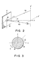
- Assume that an observer observes a
display 15 having adot 16 which is manufactured by the method of the present invention, as shown in Fig. 2. If the incidence angle ofillumination light 91 is 8, the direction of 1st-order diffractedlight 92 diffracted by a diffraction grating 18 is α, and the wavelength of the 1st-order diffractedlight 92 is λ as shown in Fig. 2, a direction Ω of the diffraction grating 18 and a pitch d (the reciprocal of a spatial frequency) of thediffraction grating 18 can be obtained by the following equations. Assume that theillumination light 91 propagates on the Y-Z plane, and the diffracted light propagates on the X-Z plane.
tan(Ω) = sin(α)/sin(ϑ)
d = λ/√sin²(ϑ) + sin²(α) - By using the above equations, the direction Ω and the pitch d of the diffraction grating 18 which are used to diffract the
illumination light 91 in an arbitrary direction can be obtained. That is, if the incidence angle ϑ of theillumination light 91, and the direction and the wavelength λ of the 1st-orderdiffracted light 92 are provided, the direction Ω and the pitch d of thediffraction grating 18 can be obtained. - Delineation of a diffraction grating by means of an electron beam scanning unit will be described below with reference to Figs. 4 and 5.
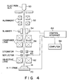
- The electron beam scanning unit comprises an
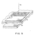
electron gun 50, analignment 52, ablanker 54, acondenser lens 56, astigmator 58, adeflector 60, anobjective lens 62, and anX-Y stage 20. An EB resist (dryplate) 14 is placed on theX-Y stage 20. Theblanker 54, thedeflector 60, and theX-Y stage 20 are connected to acomputer 66 through acontrol interface 64. An electron beam radiated from theelectron gun 50 scans thedryplate 14 under the control of thecomputer 66. - Fig. 5 shows the
dryplate 14 placed on theX-Y stage 20. Anelectron beam 70 emitted from theelectron gun 50 is used to delineatediffraction gratings 18 in units ofdots 16. Thediffraction gratings 18 are sequentially delineated in units of dots by moving theX-Y stage 20. - A sequence of operations will be described below with reference to Fig. 6.
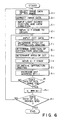
- In step a1, an Nth two-dimensional image of an object to be three-dimensionally displayed is photographed by the TV camera, and image data of the two-dimensional image is read and input to the computer. Alternatively, image data of computer graphics may be input to the computer. In addition, after all the required two-dimensional images of an object to be three-dimensionally displayed are photographed at a plurality of photographing positions and are input to the computer, an Nth two-dimensional image may be selected from the data of the plurality of two-dimensional images.
- In step b1, the two-dimensional image is corrected in the computer. This is because a two-dimensional image input to the computer often requires correction for, e.g., distortion and contrast.
- In step c1, a light source position and a view direction in observation of the display of the present invention are input to the computer.
- In step d1, the X-Y stage is moved to the origin. In step e1, dot data associated with the Nth two-dimensional image is input from a data file to the computer. Of the image data of the corrected two-dimensional image, this dot data is associated with the position, color (wavelength), and brightness of the above-mentioned dot, and the direction of the dot with respect to the stereoscopic object assumed when the two-dimensional image including the dot is fetched.
- Subsequently, in steps f1, g1, and h1, the pitch and direction of a diffraction grating and the area of the dot are determined on the basis of these data and the light source position and the view direction input in step c1. The pitch and direction of the diffraction grating are obtained by using the above-mentioned equations. The area of the dot is set to be proportional to the brightness of a portion of the object which corresponds to the dot. Note that the order of steps f1, g1, and h1 is not limited to the above order but may be variously changed.
- In step i1, the X-Y stage is moved to the position of the dot to be delineated on the basis of the dot data input in step e1. In step j1, a diffraction grating for the dot is delineated by using the above-described electron beam scanning unit. With this series of steps, delineation of the diffraction grating corresponding to one dot is completed.
- Subsequently, in step k1, the address of the data file is incremented by one in order to refer to the data of the next dot. If it is determined in step ℓ1 that image data corresponding to this address is present, the flow returns to step el to input the data of another dot, and steps f1, g1, h1, i1, j1, and k1 are repeated. This series of steps is continued until all the image data corresponding to the dots of the Nth two-dimensional image are processed. With this processing, delineation of a diffraction grating pattern based on the image data of the Nth two-dimensional image is completed.
- If it is determined in step ℓ1 that delineation of the Nth two-dimensional image is completed, the flow advances to step m1 to refer to an (N+1)th two-dimensional image. If it is determined in step n1 that the (N+1)th two-dimensional image is present, the flow returns to step a1, and steps a1 to ℓ1 are executed. With this processing, diffraction grating patterns corresponding to the (N+1)th two-dimensional image are formed.
- If the loop consisting of steps a1 to n1 is executed in this manner and it is determined in step n1 that no further three-dimensional image is present, delineation of all the diffraction gratings is completed.
- The dryplate having the diffraction grating patterns formed in this manner is used as a master plate for duplication. Duplication is performed by a well known embossing method.
- The second embodiment of the present invention will be described below with reference to Figs. 7 to 10. This embodiment is a method of manufacturing dots of diffraction gratings by interference of two laser beams.
- Fig. 7 is a perspective view for explaining a method of manufacturing a display having diffraction grating patterns by interference of two laser beams. More specifically, as shown in Fig. 7, when two
laser beams 170a and 170b are caused to interfere with each other on adryplate 114,interference fringes 118 are formed on adot 116. The cycle of theinterference fringes 118 can be changed by changing the angle at which the twolaser beams 170a and 170b interfere with each other.Dots 116 each consisting of theinterference fringes 118 are formed on thedryplate 114 while anX-Y stage 120 and a rotary (8)stage 128 are moved in accordance with commands from a computer. In this case, in order to form three types ofdots 116 representing three colors, i.e., red (R), green (G), and blue (B), laser beams of three angles are prepared. In this manner, three color spots of red (R), green (G), and blue (G) are formed at arbitrary positions on thedryplate 114 in accordance with commands from the computer. The disclosure of aforementioned U.S. Serial No. 276,469 is incorporated as a reference to determine the angles of laser beam. - Fig. 8 shows an optical system for forming dots on a dryplate. Referring to Fig. 8, the optical path of a laser beam emitted from a
laser 122 is changed by total reflection mirrors 124 and 126. The laser beam is then incident on half mirrors 132, 134, and 136 so as to be divided into four laser beams B1, B2, B3, and B4. At this time, the four laser beams B1, B2, B3, and B4 are set to have the same intensity. One of the three laser beams B1, B2, and B3 is selected by aslit 138 and is radiated on thedryplate 114 throughlenses dryplate 114 throughmirrors 144 and 146. In this case, the four laser beams B1, B2, B3, and B4 are adjusted to be concentrated at a point. In addition, the angles at which these four laser beams B1, B2, B3, and B4 are incident on thedryplate 114 are set to values calculated in advance so as to allow diffracted beams from diffraction gratings to respectively represent red (R), green (G), and blue (B). - The
dryplate 114 is placed on theX-Y stage 120. TheX-Y stage 120 is mounted on theϑ stage 128. These stages (X-Y-ϑ stage) can be moved under the control of the computer. In addition, an exposure or non-exposure operation using the four laser beams B1, B2, B3, and B4 is controlled by opening/closing of ashutter 148 arranged in front of thedryplate 114. - A method of manufacturing a display having diffraction grating patterns according to the second embodiment will be described below with reference to Fig. 9.
- In step a2, an Nth two-dimensional image of an object to be three-dimensionally displayed is photographed by a TV camera, and image data of the two-dimensional image is read and input to the computer. Alternatively, image data of computer graphics may be input to the computer. In addition, after all the required two-dimensional images of an object to be three-dimensionally displayed are photographed at a plurality of photographing positions and are input to the computer, an Nth two-dimensional image may be selected from the data of the plurality of two-dimensional images.
- In step b2, the two-dimensional image is corrected in the computer. This is because a two-dimensional image input to the computer often requires correction for, e.g., distortion and contrast.
- In step c2, a light source position and a view direction in observation of the display of the present invention are input to the computer.
- In step d2, the X-Y stage is moved to the origin. In step e2, corresponding dot data is input from a data file to the computer. Of the image data of the corrected two-dimensional image, this dot data is associated with the position, color, and brightness of the above-mentioned dot, and the direction of the dot with respect to the panorama parallax object assumed when the two-dimensional image including the dot is fetched.
- Subsequently, in steps f2, g2, and h2, the pitch and direction of a diffraction grating and an exposure time are determined on the basis of these data and the light source position and the view direction input in step c2. The direction of the diffraction grating are obtained by using the above-mentioned equations. When, angle α of a 1st-order diffracted light is small, the pitch of the diffraction gratings depends on only a reproduced light color. Therefore the pitch corresponding to the color of the dot is selected from the pitches of the R, G and B. U.S. Serial No. 276,469 on November 25, 1988 is incorporated as a reference. The exposure time can be set in accordance with a time during which the shutter of the exposure unit in Fig. 8 is opened. The exposure time is set to be proportional to the brightness of a portion of the object which corresponds to the dot. Note that the order of steps f2, g2, and h2 is not limited to the above order but may be variously changed.
- In step i2, the X-Y stage and ϑ-stage (X-Y-ϑ stage) are moved to the position of the dot to be exposed on the basis of the dot data input in step e2. In step j2, exposure of a diffraction grating for the dot is performed by using the two-beam interference unit shown in Fig. 8. With this series of steps, formation of the grating corresponding to one dot is completed.
- Subsequently, in step k2, the address of the data file is incremented by one in order to refer to the data of the next dot. If it is determined in step ℓ2 that image data corresponding to this address is present, the flow returns to step e2 to input the data of another dot, and steps f2, g2, h2, i2, j2, and k2 are repeated. This series of steps is continued until all the image data corresponding to the dots of the Nth two-dimensional image are processed. With this processing, formation of a diffraction grating pattern based on the image data of the Nth two-dimensional image is completed.
- If it is determined in step ℓ2 that the formation of the Nth two-dimensional image is completed, the flow advances to step m2 to refer to an (N+1)th two-dimensional image. If it is determined in step n2 that the (N+1)th two-dimensional image is present, the flow returns to step a2, and steps a2 to ℓ2 are executed. With this processing, diffraction grating patterns corresponding to the (N+1)th two-dimensional image are formed.
- If the loop consisting of steps a2 to n2 is executed in this manner and it is determined in step n2 that no further three-dimensional image is present, formation of all the diffraction gratings is completed.
- The dryplate having the diffraction grating patterns formed in this manner is used as a master plate for duplication. Duplication is performed by a well known embossing method.
- A method of manufacturing a display having diffraction grating patterns, comprises the steps of (a) obtaining a plurality of two-dimensional images by observing an object at a plurality of positions, and inputting images of the plurality of two-dimensional images to a computer, (b) selecting nth image data from the plurality of image data, (c) inputting data of a reproducing light source position and a view direction, (d) inputting predetermined dot data of the nth image data, (e) determining a pitch and a direction of a grating and an area of a dot on the basis of the data of the reproducing light source position and the view direction and the dot data, (f) moving an X-Y stage to a predetermined position on the basis of the dot data ano delineating the diffraction grating by using an electron scanning unit, (g) sequentially incrementing an address of the dot data and repeating the steps (d) to (f) until all data corresponding to the nth image data are processed, and (h) selecting another image data, and repeating the steps (b) to (g) until all image data are processed.
Claims (4)
tan(Ω) = sin(α)/sin(ϑ)
d = λ/√
where ϑ is the incidence angle of illumination light, α is the direction of 1st-order diffracted light, and λ is the wavelength of the 1st-order diffracted light.
tan(Ω) = sin(α)/sin(ϑ)
where ϑ is the incidence angle of illumination light, α is the direction of 1st-order diffracted light, and λ is the wavelength of the 1st-order diffracted light.
Applications Claiming Priority (2)
| Application Number | Priority Date | Filing Date | Title |
|---|---|---|---|
| JP26878089 | 1989-10-16 | ||
| JP268780/89 | 1989-10-16 |
Publications (3)
| Publication Number | Publication Date |
|---|---|
| EP0423680A2 true EP0423680A2 (en) | 1991-04-24 |
| EP0423680A3 EP0423680A3 (en) | 1992-03-18 |
| EP0423680B1 EP0423680B1 (en) | 1995-09-13 |
Family
ID=17463185
Family Applications (1)
| Application Number | Title | Priority Date | Filing Date |
|---|---|---|---|
| EP90119739A Expired - Lifetime EP0423680B1 (en) | 1989-10-16 | 1990-10-15 | Method of manufacturing display having diffraction grating patterns |
Country Status (7)
| Country | Link |
|---|---|
| US (1) | US5132812A (en) |
| EP (1) | EP0423680B1 (en) |
| JP (1) | JP2508387B2 (en) |
| AT (1) | ATE127936T1 (en) |
| AU (1) | AU616361B2 (en) |
| CA (1) | CA2027462C (en) |
| DE (1) | DE69022349T2 (en) |
Cited By (7)
| Publication number | Priority date | Publication date | Assignee | Title |
|---|---|---|---|---|
| EP0497292A2 (en) * | 1991-01-29 | 1992-08-05 | Toppan Printing Co., Ltd. | Display having diffraction grating pattern |
| EP0534616A2 (en) * | 1991-08-29 | 1993-03-31 | Fujitsu Limited | Holographic recording apparatus and holographic optical element |
| DE19623352A1 (en) * | 1996-06-12 | 1997-12-18 | Kurz Leonhard Fa | Process for producing printing or embossing cylinders with a spatially patterned surface |
| WO2006108539A3 (en) * | 2005-04-14 | 2006-12-21 | Giesecke & Devrient Gmbh | Diffraction grating and method for producing the same |
| EP1676157B1 (en) * | 2003-10-15 | 2009-04-15 | Giesecke & Devrient GmbH | Method for the creation of a planar or curved grating image |
| US7986459B2 (en) | 2005-07-14 | 2011-07-26 | Giesecke & Devrient Gmbh | Grid image and method for the production thereof |
| CN105511074A (en) * | 2016-01-06 | 2016-04-20 | 苏州大学 | Real time variable parameter micro-nano optical field modulation system and interference lithography system |
Families Citing this family (50)
| Publication number | Priority date | Publication date | Assignee | Title |
|---|---|---|---|---|
| JP2725913B2 (en) * | 1991-08-29 | 1998-03-11 | 富士通株式会社 | Hologram drawing device |
| JP2774398B2 (en) * | 1991-09-17 | 1998-07-09 | 富士通株式会社 | Hologram making device |
| JPH0572407A (en) * | 1991-09-11 | 1993-03-26 | Toppan Printing Co Ltd | Diffraction grating plotter |
| JP2830530B2 (en) * | 1991-09-11 | 1998-12-02 | 凸版印刷株式会社 | Diffraction grating plotter |
| JPH0572405A (en) * | 1991-09-11 | 1993-03-26 | Toppan Printing Co Ltd | Diffraction grating plotter |
| US6219015B1 (en) | 1992-04-28 | 2001-04-17 | The Board Of Directors Of The Leland Stanford, Junior University | Method and apparatus for using an array of grating light valves to produce multicolor optical images |
| JPH0635391A (en) * | 1992-07-20 | 1994-02-10 | Fujitsu Ltd | Stereoscopic display device |
| JPH0635392A (en) * | 1992-07-20 | 1994-02-10 | Fujitsu Ltd | Stereoscopic display device |
| US5991078A (en) * | 1992-08-19 | 1999-11-23 | Dai Nippon Printing Co., Ltd. | Display medium employing diffraction grating and method of producing diffraction grating assembly |
| EP0748459A4 (en) * | 1994-02-28 | 1998-08-19 | Mikoh Technology Ltd | Difraction surfaces and methods for the manufacture thereof |
| US5798743A (en) * | 1995-06-07 | 1998-08-25 | Silicon Light Machines | Clear-behind matrix addressing for display systems |
| US5629801A (en) * | 1995-06-07 | 1997-05-13 | Silicon Light Machines | Diffraction grating light doubling collection system |
| US5841579A (en) | 1995-06-07 | 1998-11-24 | Silicon Light Machines | Flat diffraction grating light valve |
| US5661592A (en) * | 1995-06-07 | 1997-08-26 | Silicon Light Machines | Method of making and an apparatus for a flat diffraction grating light valve |
| US6064404A (en) * | 1996-11-05 | 2000-05-16 | Silicon Light Machines | Bandwidth and frame buffer size reduction in a digital pulse-width-modulated display system |
| AUPO384796A0 (en) * | 1996-11-26 | 1996-12-19 | Commonwealth Scientific And Industrial Research Organisation | Colour image diffractive device |
| US5982553A (en) | 1997-03-20 | 1999-11-09 | Silicon Light Machines | Display device incorporating one-dimensional grating light-valve array |
| US6088102A (en) | 1997-10-31 | 2000-07-11 | Silicon Light Machines | Display apparatus including grating light-valve array and interferometric optical system |
| US6271808B1 (en) | 1998-06-05 | 2001-08-07 | Silicon Light Machines | Stereo head mounted display using a single display device |
| US6101036A (en) | 1998-06-23 | 2000-08-08 | Silicon Light Machines | Embossed diffraction grating alone and in combination with changeable image display |
| US6130770A (en) | 1998-06-23 | 2000-10-10 | Silicon Light Machines | Electron gun activated grating light valve |
| US6215579B1 (en) | 1998-06-24 | 2001-04-10 | Silicon Light Machines | Method and apparatus for modulating an incident light beam for forming a two-dimensional image |
| US6303986B1 (en) | 1998-07-29 | 2001-10-16 | Silicon Light Machines | Method of and apparatus for sealing an hermetic lid to a semiconductor die |
| US6747781B2 (en) | 2001-06-25 | 2004-06-08 | Silicon Light Machines, Inc. | Method, apparatus, and diffuser for reducing laser speckle |
| US6782205B2 (en) | 2001-06-25 | 2004-08-24 | Silicon Light Machines | Method and apparatus for dynamic equalization in wavelength division multiplexing |
| US6829092B2 (en) | 2001-08-15 | 2004-12-07 | Silicon Light Machines, Inc. | Blazed grating light valve |
| US6800238B1 (en) | 2002-01-15 | 2004-10-05 | Silicon Light Machines, Inc. | Method for domain patterning in low coercive field ferroelectrics |
| US6767751B2 (en) | 2002-05-28 | 2004-07-27 | Silicon Light Machines, Inc. | Integrated driver process flow |
| US6728023B1 (en) | 2002-05-28 | 2004-04-27 | Silicon Light Machines | Optical device arrays with optimized image resolution |
| US6822797B1 (en) | 2002-05-31 | 2004-11-23 | Silicon Light Machines, Inc. | Light modulator structure for producing high-contrast operation using zero-order light |
| US6829258B1 (en) | 2002-06-26 | 2004-12-07 | Silicon Light Machines, Inc. | Rapidly tunable external cavity laser |
| US6813059B2 (en) | 2002-06-28 | 2004-11-02 | Silicon Light Machines, Inc. | Reduced formation of asperities in contact micro-structures |
| US6801354B1 (en) | 2002-08-20 | 2004-10-05 | Silicon Light Machines, Inc. | 2-D diffraction grating for substantially eliminating polarization dependent losses |
| US6712480B1 (en) | 2002-09-27 | 2004-03-30 | Silicon Light Machines | Controlled curvature of stressed micro-structures |
| US6806997B1 (en) | 2003-02-28 | 2004-10-19 | Silicon Light Machines, Inc. | Patterned diffractive light modulator ribbon for PDL reduction |
| US6829077B1 (en) | 2003-02-28 | 2004-12-07 | Silicon Light Machines, Inc. | Diffractive light modulator with dynamically rotatable diffraction plane |
| JP4779415B2 (en) * | 2005-04-18 | 2011-09-28 | 大日本印刷株式会社 | Image forming method and image display body |
| WO2007089770A2 (en) * | 2006-01-31 | 2007-08-09 | Polychromix Corporation | Hand-held ir spectrometer with a fixed grating and a diffractive mems-array |
| JP5488581B2 (en) * | 2006-08-22 | 2014-05-14 | 大日本印刷株式会社 | Method for producing diffraction grating recording medium expressing three-dimensional pattern |
| US7891818B2 (en) | 2006-12-12 | 2011-02-22 | Evans & Sutherland Computer Corporation | System and method for aligning RGB light in a single modulator projector |
| US8358317B2 (en) | 2008-05-23 | 2013-01-22 | Evans & Sutherland Computer Corporation | System and method for displaying a planar image on a curved surface |
| US8702248B1 (en) | 2008-06-11 | 2014-04-22 | Evans & Sutherland Computer Corporation | Projection method for reducing interpixel gaps on a viewing surface |
| KR20100002032A (en) * | 2008-06-24 | 2010-01-06 | 삼성전자주식회사 | Image generating method, image processing method, and apparatus thereof |
| WO2009157713A2 (en) * | 2008-06-24 | 2009-12-30 | Samsung Electronics Co., Ltd. | Image processing method and apparatus |
| KR101560617B1 (en) * | 2008-09-10 | 2015-10-16 | 삼성전자주식회사 | Light Generating Apparatus and Method For Controlling the Same |
| US8077378B1 (en) | 2008-11-12 | 2011-12-13 | Evans & Sutherland Computer Corporation | Calibration system and method for light modulation device |
| JP5419540B2 (en) * | 2009-05-18 | 2014-02-19 | パナソニック株式会社 | Structural color body |
| US9641826B1 (en) | 2011-10-06 | 2017-05-02 | Evans & Sutherland Computer Corporation | System and method for displaying distant 3-D stereo on a dome surface |
| CN103246195B (en) * | 2013-05-08 | 2015-12-02 | 苏州苏大维格光电科技股份有限公司 | Three-dimensional laser Method of printing and system |
| WO2017117751A1 (en) | 2016-01-06 | 2017-07-13 | 苏州大学 | Real-time variable-parameter micro-nano optical field modulation system and interference photoetching system |
Citations (4)
| Publication number | Priority date | Publication date | Assignee | Title |
|---|---|---|---|---|
| US3832027A (en) * | 1969-03-12 | 1974-08-27 | Bell Telephone Labor Inc | Synthetic hologram generation from a plurality of two-dimensional views |
| JPS60156004A (en) * | 1984-01-12 | 1985-08-16 | Toppan Printing Co Ltd | Exposure device of diffraction grating |
| EP0213726A2 (en) * | 1985-07-26 | 1987-03-11 | Matsushita Electric Industrial Co., Ltd. | Holographic multiplexer/demultiplexer and its manufacturing method |
| EP0357837A2 (en) * | 1988-09-07 | 1990-03-14 | Toppan Printing Co., Ltd. | Method for producing a display with a diffraction grating pattern and a display produced by the method |
Family Cites Families (7)
| Publication number | Priority date | Publication date | Assignee | Title |
|---|---|---|---|---|
| US3646335A (en) * | 1969-02-11 | 1972-02-29 | Us Army | Recorder correlator using scanning recorder devices |
| US4498740A (en) * | 1983-04-18 | 1985-02-12 | Aerodyne, Research, Inc. | Hologram writer and method |
| US4846552A (en) * | 1986-04-16 | 1989-07-11 | The United States Of America As Represented By The Secretary Of The Air Force | Method of fabricating high efficiency binary planar optical elements |
| US4778262A (en) * | 1986-10-14 | 1988-10-18 | American Bank Note Holographics, Inc. | Computer aided holography and holographic computer graphics |
| US4929823A (en) * | 1987-10-05 | 1990-05-29 | Matsushita Electric Industrial Co., Ltd. | Optical pickup head with holographic servo signal detection using a spot size detection system |
| US4896044A (en) * | 1989-02-17 | 1990-01-23 | Purdue Research Foundation | Scanning tunneling microscope nanoetching method |
| US5016953A (en) * | 1989-08-31 | 1991-05-21 | Hughes Aircraft Company | Reduction of noise in computer generated holograms |
-
1990
- 1990-09-05 JP JP2233105A patent/JP2508387B2/en not_active Expired - Lifetime
- 1990-10-12 AU AU64597/90A patent/AU616361B2/en not_active Expired
- 1990-10-12 CA CA002027462A patent/CA2027462C/en not_active Expired - Lifetime
- 1990-10-15 US US07/597,229 patent/US5132812A/en not_active Expired - Lifetime
- 1990-10-15 DE DE69022349T patent/DE69022349T2/en not_active Expired - Lifetime
- 1990-10-15 AT AT90119739T patent/ATE127936T1/en not_active IP Right Cessation
- 1990-10-15 EP EP90119739A patent/EP0423680B1/en not_active Expired - Lifetime
Patent Citations (4)
| Publication number | Priority date | Publication date | Assignee | Title |
|---|---|---|---|---|
| US3832027A (en) * | 1969-03-12 | 1974-08-27 | Bell Telephone Labor Inc | Synthetic hologram generation from a plurality of two-dimensional views |
| JPS60156004A (en) * | 1984-01-12 | 1985-08-16 | Toppan Printing Co Ltd | Exposure device of diffraction grating |
| EP0213726A2 (en) * | 1985-07-26 | 1987-03-11 | Matsushita Electric Industrial Co., Ltd. | Holographic multiplexer/demultiplexer and its manufacturing method |
| EP0357837A2 (en) * | 1988-09-07 | 1990-03-14 | Toppan Printing Co., Ltd. | Method for producing a display with a diffraction grating pattern and a display produced by the method |
Non-Patent Citations (2)
| Title |
|---|
| APPLIED OPTICS, vol. 15, no. 11, November 1976, pages 2722-2729; T. YATAGAI: "Stereoscopic approach to 3-D display using computer-generated holograms" * |
| PATENT ABSTRACTS OF JAPAN, vol. 9, no. 329 (P-416)[2052], 24th December 1985; & JP-A-60 156 004 (TOPPAN INSATSU K.K.) 16-08-1985 * |
Cited By (13)
| Publication number | Priority date | Publication date | Assignee | Title |
|---|---|---|---|---|
| EP0497292A3 (en) * | 1991-01-29 | 1994-02-16 | Toppan Printing Co Ltd | |
| EP0497292A2 (en) * | 1991-01-29 | 1992-08-05 | Toppan Printing Co., Ltd. | Display having diffraction grating pattern |
| US5301062A (en) * | 1991-01-29 | 1994-04-05 | Toppan Printing Co., Ltd. | Display having diffraction grating pattern |
| US5892597A (en) * | 1991-08-29 | 1999-04-06 | Fujitsu Limited | Holographic recording apparatus and holographic optical element |
| EP0534616A3 (en) * | 1991-08-29 | 1993-08-11 | Fujitsu Limited | Holographic recording apparatus and holographic optical element |
| EP0534616A2 (en) * | 1991-08-29 | 1993-03-31 | Fujitsu Limited | Holographic recording apparatus and holographic optical element |
| DE19623352A1 (en) * | 1996-06-12 | 1997-12-18 | Kurz Leonhard Fa | Process for producing printing or embossing cylinders with a spatially patterned surface |
| DE19623352C2 (en) * | 1996-06-12 | 1999-11-11 | Kurz Leonhard Fa | Process for producing printing or embossing cylinders with a spatially patterned surface |
| EP1676157B1 (en) * | 2003-10-15 | 2009-04-15 | Giesecke & Devrient GmbH | Method for the creation of a planar or curved grating image |
| WO2006108539A3 (en) * | 2005-04-14 | 2006-12-21 | Giesecke & Devrient Gmbh | Diffraction grating and method for producing the same |
| US7986459B2 (en) | 2005-07-14 | 2011-07-26 | Giesecke & Devrient Gmbh | Grid image and method for the production thereof |
| CN105511074A (en) * | 2016-01-06 | 2016-04-20 | 苏州大学 | Real time variable parameter micro-nano optical field modulation system and interference lithography system |
| CN105511074B (en) * | 2016-01-06 | 2018-01-09 | 苏州大学 | The micro-nano light field modulating system of real time-varying parameter and interference lithography system |
Also Published As
| Publication number | Publication date |
|---|---|
| US5132812A (en) | 1992-07-21 |
| DE69022349T2 (en) | 1996-02-08 |
| AU6459790A (en) | 1991-05-23 |
| ATE127936T1 (en) | 1995-09-15 |
| EP0423680A3 (en) | 1992-03-18 |
| CA2027462C (en) | 1998-08-11 |
| EP0423680B1 (en) | 1995-09-13 |
| JPH03206401A (en) | 1991-09-09 |
| CA2027462A1 (en) | 1991-04-17 |
| JP2508387B2 (en) | 1996-06-19 |
| AU616361B2 (en) | 1991-10-24 |
| DE69022349D1 (en) | 1995-10-19 |
Similar Documents
| Publication | Publication Date | Title |
|---|---|---|
| EP0423680B1 (en) | Method of manufacturing display having diffraction grating patterns | |
| US5058992A (en) | Method for producing a display with a diffraction grating pattern and a display produced by the method | |
| US5301062A (en) | Display having diffraction grating pattern | |
| US5926294A (en) | Three-dimensional image display device having an elementary hologram panel and method for manufacturing the elementary hologram panel | |
| JP2979951B2 (en) | Display with diffraction grating pattern | |
| JPH05273500A (en) | Display having diffraction grating pattern | |
| JPH0812285B2 (en) | Display having diffraction grating pattern and method of manufacturing the same | |
| JP2920971B2 (en) | Manufacturing method of display with good diffraction grating pattern | |
| JP2745902B2 (en) | Display with diffraction grating pattern | |
| JP2976774B2 (en) | Display with diffraction grating pattern | |
| Takahashi et al. | Three-dimensional grating images | |
| JP2001083866A (en) | Hologram recording medium and manufactuing method thereof | |
| JP2630047B2 (en) | Display having diffraction grating pattern and manufacturing method thereof | |
| RU98110055A (en) | OPTICALLY CONTROLLED DEVICE (OVD), AND ALSO METHOD AND DEVICE FOR MANUFACTURING, BY RECORDING, OPTICALLY CONTROLLED DEVICE (OVD) | |
| JPH0820563B2 (en) | Display with diffraction grating pattern | |
| JPH0272319A (en) | Display with diffraction grating pattern and its manufacture | |
| JP3932599B2 (en) | Diffraction grating pattern | |
| van Nuland et al. | Development of an office holoprinter V | |
| US5222156A (en) | Object information processing apparatus | |
| KR101962213B1 (en) | Manufacturing method of glass master having stereo scopic image using the diffraction of surfacerelief's fine pixels | |
| JP3231650B2 (en) | Diffraction grating pattern | |
| JPH07146635A (en) | Hologram recording medium and its formation | |
| JP2000329919A (en) | Diffraction grating pattern and its production | |
| JPH0553493A (en) | Manufacture of lipman-holographic-stereogram | |
| JP2792275B2 (en) | Hologram fabrication method |
Legal Events
| Date | Code | Title | Description |
|---|---|---|---|
| PUAI | Public reference made under article 153(3) epc to a published international application that has entered the european phase |
Free format text: ORIGINAL CODE: 0009012 |
|
| 17P | Request for examination filed |
Effective date: 19901015 |
|
| AK | Designated contracting states |
Kind code of ref document: A2 Designated state(s): AT CH DE FR GB LI |
|
| PUAL | Search report despatched |
Free format text: ORIGINAL CODE: 0009013 |
|
| AK | Designated contracting states |
Kind code of ref document: A3 Designated state(s): AT CH DE FR GB LI |
|
| 17Q | First examination report despatched |
Effective date: 19940202 |
|
| GRAA | (expected) grant |
Free format text: ORIGINAL CODE: 0009210 |
|
| AK | Designated contracting states |
Kind code of ref document: B1 Designated state(s): AT CH DE FR GB LI |
|
| REF | Corresponds to: |
Ref document number: 127936 Country of ref document: AT Date of ref document: 19950915 Kind code of ref document: T |
|
| ET | Fr: translation filed | ||
| REF | Corresponds to: |
Ref document number: 69022349 Country of ref document: DE Date of ref document: 19951019 |
|
| PLBE | No opposition filed within time limit |
Free format text: ORIGINAL CODE: 0009261 |
|
| STAA | Information on the status of an ep patent application or granted ep patent |
Free format text: STATUS: NO OPPOSITION FILED WITHIN TIME LIMIT |
|
| 26N | No opposition filed | ||
| REG | Reference to a national code |
Ref country code: GB Ref legal event code: IF02 |
|
| REG | Reference to a national code |
Ref country code: CH Ref legal event code: PFA Owner name: TOPPAN PRINTING CO., LTD Free format text: TOPPAN PRINTING CO., LTD#5-1, TAITO 1-CHOME#TAITO-KU/TOKYO (JP) -TRANSFER TO- TOPPAN PRINTING CO., LTD#5-1, TAITO 1-CHOME#TAITO-KU/TOKYO (JP) |
|
| PGFP | Annual fee paid to national office [announced via postgrant information from national office to epo] |
Ref country code: AT Payment date: 20091013 Year of fee payment: 20 Ref country code: CH Payment date: 20091014 Year of fee payment: 20 Ref country code: DE Payment date: 20091008 Year of fee payment: 20 |
|
| PGFP | Annual fee paid to national office [announced via postgrant information from national office to epo] |
Ref country code: GB Payment date: 20091014 Year of fee payment: 20 Ref country code: FR Payment date: 20091029 Year of fee payment: 20 |
|
| REG | Reference to a national code |
Ref country code: CH Ref legal event code: PL |
|
| REG | Reference to a national code |
Ref country code: GB Ref legal event code: PE20 Expiry date: 20101014 |
|
| PG25 | Lapsed in a contracting state [announced via postgrant information from national office to epo] |
Ref country code: GB Free format text: LAPSE BECAUSE OF EXPIRATION OF PROTECTION Effective date: 20101014 |
|
| PG25 | Lapsed in a contracting state [announced via postgrant information from national office to epo] |
Ref country code: DE Free format text: LAPSE BECAUSE OF EXPIRATION OF PROTECTION Effective date: 20101015 |