EP0435237B1 - Electrostatic miniature valve and method for its fabrication - Google Patents
Electrostatic miniature valve and method for its fabrication Download PDFInfo
- Publication number
- EP0435237B1 EP0435237B1 EP90125446A EP90125446A EP0435237B1 EP 0435237 B1 EP0435237 B1 EP 0435237B1 EP 90125446 A EP90125446 A EP 90125446A EP 90125446 A EP90125446 A EP 90125446A EP 0435237 B1 EP0435237 B1 EP 0435237B1
- Authority
- EP
- European Patent Office
- Prior art keywords
- valve
- silicon nitride
- layer
- valve seat
- electrode
- Prior art date
- Legal status (The legal status is an assumption and is not a legal conclusion. Google has not performed a legal analysis and makes no representation as to the accuracy of the status listed.)
- Expired - Lifetime
Links
Images


Classifications
-
- F—MECHANICAL ENGINEERING; LIGHTING; HEATING; WEAPONS; BLASTING
- F16—ENGINEERING ELEMENTS AND UNITS; GENERAL MEASURES FOR PRODUCING AND MAINTAINING EFFECTIVE FUNCTIONING OF MACHINES OR INSTALLATIONS; THERMAL INSULATION IN GENERAL
- F16K—VALVES; TAPS; COCKS; ACTUATING-FLOATS; DEVICES FOR VENTING OR AERATING
- F16K99/00—Subject matter not provided for in other groups of this subclass
- F16K99/0001—Microvalves
-
- F—MECHANICAL ENGINEERING; LIGHTING; HEATING; WEAPONS; BLASTING
- F15—FLUID-PRESSURE ACTUATORS; HYDRAULICS OR PNEUMATICS IN GENERAL
- F15C—FLUID-CIRCUIT ELEMENTS PREDOMINANTLY USED FOR COMPUTING OR CONTROL PURPOSES
- F15C5/00—Manufacture of fluid circuit elements; Manufacture of assemblages of such elements integrated circuits
-
- F—MECHANICAL ENGINEERING; LIGHTING; HEATING; WEAPONS; BLASTING
- F16—ENGINEERING ELEMENTS AND UNITS; GENERAL MEASURES FOR PRODUCING AND MAINTAINING EFFECTIVE FUNCTIONING OF MACHINES OR INSTALLATIONS; THERMAL INSULATION IN GENERAL
- F16K—VALVES; TAPS; COCKS; ACTUATING-FLOATS; DEVICES FOR VENTING OR AERATING
- F16K99/00—Subject matter not provided for in other groups of this subclass
- F16K99/0001—Microvalves
- F16K99/0003—Constructional types of microvalves; Details of the cutting-off member
- F16K99/0005—Lift valves
- F16K99/0007—Lift valves of cantilever type
-
- F—MECHANICAL ENGINEERING; LIGHTING; HEATING; WEAPONS; BLASTING
- F16—ENGINEERING ELEMENTS AND UNITS; GENERAL MEASURES FOR PRODUCING AND MAINTAINING EFFECTIVE FUNCTIONING OF MACHINES OR INSTALLATIONS; THERMAL INSULATION IN GENERAL
- F16K—VALVES; TAPS; COCKS; ACTUATING-FLOATS; DEVICES FOR VENTING OR AERATING
- F16K99/00—Subject matter not provided for in other groups of this subclass
- F16K99/0001—Microvalves
- F16K99/0003—Constructional types of microvalves; Details of the cutting-off member
- F16K99/0015—Diaphragm or membrane valves
-
- F—MECHANICAL ENGINEERING; LIGHTING; HEATING; WEAPONS; BLASTING
- F16—ENGINEERING ELEMENTS AND UNITS; GENERAL MEASURES FOR PRODUCING AND MAINTAINING EFFECTIVE FUNCTIONING OF MACHINES OR INSTALLATIONS; THERMAL INSULATION IN GENERAL
- F16K—VALVES; TAPS; COCKS; ACTUATING-FLOATS; DEVICES FOR VENTING OR AERATING
- F16K99/00—Subject matter not provided for in other groups of this subclass
- F16K99/0001—Microvalves
- F16K99/0034—Operating means specially adapted for microvalves
- F16K99/0042—Electric operating means therefor
- F16K99/0051—Electric operating means therefor using electrostatic means
-
- F—MECHANICAL ENGINEERING; LIGHTING; HEATING; WEAPONS; BLASTING
- F16—ENGINEERING ELEMENTS AND UNITS; GENERAL MEASURES FOR PRODUCING AND MAINTAINING EFFECTIVE FUNCTIONING OF MACHINES OR INSTALLATIONS; THERMAL INSULATION IN GENERAL
- F16K—VALVES; TAPS; COCKS; ACTUATING-FLOATS; DEVICES FOR VENTING OR AERATING
- F16K99/00—Subject matter not provided for in other groups of this subclass
- F16K2099/0073—Fabrication methods specifically adapted for microvalves
- F16K2099/0074—Fabrication methods specifically adapted for microvalves using photolithography, e.g. etching
-
- F—MECHANICAL ENGINEERING; LIGHTING; HEATING; WEAPONS; BLASTING
- F16—ENGINEERING ELEMENTS AND UNITS; GENERAL MEASURES FOR PRODUCING AND MAINTAINING EFFECTIVE FUNCTIONING OF MACHINES OR INSTALLATIONS; THERMAL INSULATION IN GENERAL
- F16K—VALVES; TAPS; COCKS; ACTUATING-FLOATS; DEVICES FOR VENTING OR AERATING
- F16K99/00—Subject matter not provided for in other groups of this subclass
- F16K2099/0073—Fabrication methods specifically adapted for microvalves
- F16K2099/008—Multi-layer fabrications
-
- F—MECHANICAL ENGINEERING; LIGHTING; HEATING; WEAPONS; BLASTING
- F16—ENGINEERING ELEMENTS AND UNITS; GENERAL MEASURES FOR PRODUCING AND MAINTAINING EFFECTIVE FUNCTIONING OF MACHINES OR INSTALLATIONS; THERMAL INSULATION IN GENERAL
- F16K—VALVES; TAPS; COCKS; ACTUATING-FLOATS; DEVICES FOR VENTING OR AERATING
- F16K99/00—Subject matter not provided for in other groups of this subclass
- F16K99/0001—Microvalves
- F16K99/0034—Operating means specially adapted for microvalves
Definitions
- the present invention relates to an electrostatic miniature valve and a method for its fabrication.
- microvalves There are several types of microvalves including one in which a miniature valve is fabricated from two micromachined pieces of material which must be assembled after processing.
- Another miniature valve has an enclosed chamber with flow inlet and flow outlet on the same side of a silicon wafer.
- EP-A 0 276 156 shows an electrostatic miniature valve comprising the features listed in the preamble of claim 1.
- the valve seat is provided in a metal plate such as a stainless steel plate or in a glass plate which has a metal film formed on a surface thereof.
- a conical nozzle is etched into said plate and thereafter a first insulator layer of photosensitive polyimid is formed on the surface of the nozzle plate and thereafter is exposed to light for forming a first opening in the region of the nozzle and forming further openings laterally displaced but immediately adjacent to said nozzle.
- a metal film is formed by non-electrolytic nickel plating to provide a conductor layer having a high adhering property to the above-mentioned insulating layer. Then a second insulating layer is deposited to isolate the electrode plate.
- a spacer is formed by sputtering copper on a protective layer including a location opposing the nozzle.
- This spacer in the area of the nozzle has the shape of said nozzle.
- a next step is forming a photoresist layer on a surface of the spacer other than the portion opposing the nozzle, and in a subsequent valve beam forming step a metal film is formed on the portion of the surface of the spacer on which the photoresist layer is not deposited in order to form a support frame of a square profile and a valve beam having opposite ends connected contiguously to said support frame.
- the metal film is formed by nickel plating. The opposite ends of the valve beam are connected to the nozzle plate by way of the support frame.
- a central portion of the spacer is removed by etching, and the substrate is exfoliated from the nozzle plate.
- Making the substrate from stainless steel and the nozzle plate from nickel facilitates the separation of those two parts.
- the shape of the nozzle plate region opposite the nozzle is the same conical shape as that of the nozzle.
- the valve beam carrying the closure member is formed by providing said openings adjacent to the valve closure member, which openings extend in parallel to said valve beam. It is an object of the invention to improve the structure of such an electrostatic miniature valve, and in particular to facilitate its fabrication.
- the miniature valve is made as an integral structure on a single piece of silicon and constitutes a flow through valve with a flow inlet and a flow outlet on opposite sides of the silicon wafer.
- This is a miniature integral thin film bleed valve in which the flat closure plate or member surface conforms to the surface of the valve orifice plate or member.
- the valve closure plate has flow holes through the plate, the holes being near but laterally displaced from the valve orifice that reduce the effective area the gas pressure is pushing against when closing, making it easier to close the valve.
- the closure plate of the microvalve can be in the form of a cantilever, a beam attached at two sides, or a diaphragm attached at four sides with flow holes through the diaphragm. Further details are characterized in the dependent claims and can be seen from the following description of preferred embodiments.
- Electrostatically operated bleed valves depend on extremely close spacings between the valve seat member electrode and the closure member electrode over an area substantially broader than the flow orifice to obtain effective closures against high fluid pressures if excessive operating voltages are to be avoided.
- the electrostatically generated force increases inversely with the square of the separation distance. Therefore a lack of matching of the two electrode surfaces that may arise from differences of curvature, irregular surfaces, or warping can degrade the valve performance.
- the use of a raised seat can seriously affect the performance in that the standoff effect of the seat prevents the closest approach of the two electrodes in the area surrounding the seat.
- any bimorph bending effect due to asymmetry in the thickness properties of the closure member may prevent complete closure at normal applied voltages.
- This invention avoids or minimizes these difficulties by fabricating the device by means of one integral operation by depositing and delineating a set of stacked thin film layers such that separate handling of any part of the structure is never required.
- This method of fabrication enables the use of a conformal structure for the electrode members that is obtained by etching out an extremely thin sacrificial layer of uniform thickness such that any shape irregularity on the lower electrode member surface is matched by its negative image on the upper electrode member surface. Hence the surfaces fit together in closure after etching.
- the exposed member surfaces are composed of chemically inert, high quality silicon nitride which is not significantly attacked by the etchant.
- the invention uses closure member area shapes and thin dimensions, one micron thick or less, that allow flexing mainly at the edges when in the closed position, thus enabling conformal closure over all of the closure member's main area even for moderate asymmetry in the thickness properties of the closure member.
- An additional advantage of this invention is that the pneumatic force on the closure member when closing and when in the closed position can be minimized, if desired, by the use of flow-through holes located in the closure member adjacent to the valve orifice holes.
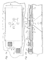
- FIG. 1a is a top plan view of a preferred embodiment of the microvalve shown more clearly in the sectional view of Fig. 1b.
- a substrate 1 is preferably of single crystal silicon in which a wafer has been cut from a single crystal boule. Multiple valves may be simultaneously made in the same wafer if desired, and later separated, as is common in semiconductor chip technology.
- the miniature valve includes broadly the following major components; an inlet orifice 2 which is formed by etching through the substrate 1 from the backside, a valve base plate 3, which is part of a thin film dielectric layer means 30, preferably of silicon nitride, (Si3N4), formed on the surface 31 of the silicon substrate 1, a dielectric closure plate 4, that is a thin free standing flexible dielectric region that has been released from the main body of layer means 30 by the removal of a sacrificial film, leaving a thin gap 5 between the closure plate 4 and the base plate 3.
- the closure plate 4 contains one or more flow-through outlet holes 6 adjacent to the inlet orifice 2 but laterally offset from the orifice. Four such adjacent flow-through holes 6 are shown in Fig.
- the total area of the outlet holes 6 is preferably designed to be equal to or larger than the area of the orifice 2.
- Outlet flow slots 7 formed along two sides 32 and 33 of the closure plate 4 leave the closure plate attached to the rest of the structure on two sides generally indicated at 34 and 35.
- the area of the closure plate 4 is designed to be 10-100 times the area of the orifice.
- electrode 8 Embedded in the base plate 3 is electrode 8 and embedded in the closure plate 4 is an electrode 9.
- the lower electrode 8 is completely encapsulated by dielectric to electrically isolate it from the silicon substrate 1 and the upper electrode 9.
- Fig. 1b is shown in the unenergized normally open position.
- Fig. 2a shows the same embodiment of the valve as is shown in Fig. 1b, but Fig. 2a shows the valve in the closed position.
- the surface 36 of closure plate 4 will move down to touch surface 37 of base plate 3.
- Figs. 1 and 2 The operation of the miniature valve is as follows, now referring to Figs. 1 and 2.
- gas enters the valve through the inlet orifice 2 and flows through the valve and exits through the outlet orifice holes 6 in the closure plate 4 and the outlet holes 7 along the sides of the closure plate.
- a voltage is applied between the upper electrode plate 9 and lower electrode plate 8 at the contact pads 10,11 there is an electrostatic force between the electrode plates that is directly proportional to the square of the applied voltage that will pull the closure plate 4 against the valve base plate 3 as illustrated in Fig. 2a and stop the flow of gas through the valve.
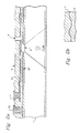
- FIG. 2b is an enlargement of a section of the mating or opposing surfaces of the base plate 3 and the closure plate 4. It shows that closure plate 4 and the base plate 3 will fit together with conformal surfaces. Because the valve is made by a succession of thin film depositions any surface irregularities or asperities in the silicon substrate or any film depositions will be replicated throughout subsequent film depositions. Therefore referring to Fig. 1b, when the thin sacrificial layer is removed leaving the gap 5, the top surface of the base plate 3 will be mirror imaged in the bottom surface of the closure plate 4, so that when the two surfaces are pressed together in the closed position of the valve as in Figs. 2a and 2b there will be a conformal mating of the closure plate 4 and base plate 3 surfaces giving tight sealing of the valve over the majority of the area of the closure plate 4.
- the valve may be operated as a two position valve with fully open and fully closed positions by applying a d.c. voltage between the electrodes or it may be operated as a proportional control valve by applying a voltage proportional to the voltage necessary to close the valve. It may also be operated with a pulse width modulated voltage signal to modulate the gas flow through the valve.
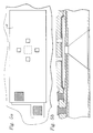
- Fig. 3a illustrates a valve with all of the thin film layers deposited and patterned but the final etching has not yet been performed.
- the fabrication sequence begins with a (100) silicon wafer 1 that has both sides polished to a semiconductor device-quality mirror finish.
- a silicon nitride film 12 is deposited on the front side of the wafer to passivate the surface and electrically isolate the lower electrode 8 from the silicon wafer 1.
- Another silicon nitride film 13 is deposited on the backside of the wafer to passivate the back surface of the wafer and protect it during the final etching steps of the processing.
- the backside silicon nitride film 13 is patterned to form the backside inlet orifice opening 14 which will be etched later in the processing.
- a metal film is then deposited and patterned on the frontside of the wafer to form the lower electrode 8, and it is then passivated by a silicon nitride film 15.
- the silicon nitride film on the frontside is then patterned and etched to open a via to the silicon surface 16.
- This via pattern 16 defines the frontside of the inlet orifice.
- the via is formed using a plasma etch.
- a thin film of material is then deposited and patterned that will serve as a sacrificial layer 17 that will be removed later in the processing.
- This sacrificial layer 17 serves as a spacer between the valve base plate 3 and the valve closure plate 4 so that when it is removed later in the process, the closure plate 4 will be released and free to move.
- the sacrificial layer 17 can be any material, a metal or an insulator that can be deposited in thin layers, patterned, and later removed with an etch that does not attack any of the other films that would be exposed at the time of the etching. Examples of sacrificial layers that can be used are aluminum or silicon dioxide.
- Each of these materials can be removed using an etch that will not attack the silicon nitride layers used in the valve structure or any of the other metals used in the contacting pad areas 10 and 11.
- a thin layer of silicon nitride 18 is deposited over the sacrificial layer to form the bottom layer of the valve closure plate 4 and to provide passivation of the upper electrode and to electrically isolate the upper electrode 9 from the bottom electrode 8.
- Fig. 3b illustrates the conformal nature of the film depositions described previously through an illustrative enlargement of the film interfaces on either side of the sacrificial spacer layer 17. Any surface irregularities are transmitted up and replicated through subsequent film depositions. This results in conformal mating surfaces between the valve base plate 3 and the valve closure plate 4 after the removal of the sacrificial layer 17.
- a metal layer is then deposited and patterned to form the upper electrode 9.
- a silicon nitride layer 19 is then deposited over the upper electrode 9 to passivate the electrode and finish the formation of the closure plate 4.
- This silicon nitride layer 19 is typically a thicker film than the layer 18 under the upper electrode 9 to give the closure plate 4 added strength when the sacrificial layer 17 is removed.
- the total thickness of the closure plate 4, made up of the nitride layers 18 and 19 and the upper electrode 9, is typically in the range of 1 to 1.5 microns.
- the silicon nitride films 18 and 19 that make up the closure plate 4 are deposited in a stress controlled manner such that when the closure plate is released from the substrate structure by the removal of the sacrificial layer 17, the closure plate 4 remains flat and free from any buckling or warping to preserve the conformal mating surfaces of the closure plate 4 and the valve base plate 3.
- the outlet flow openings 6 and 7 are formed by etching vias through the closure plate 4 using a dry plasma etch. These flow holes also act as access vias for the introduction of an etchant for the removal of the sacrificial layer during the final etching steps.
- the fabrication of the valve is completed by anisotropically etching the silicon wafer in KOH to form the inlet port 2.
- the sacrificial layer, 17 in Fig. 3a is then removed using an etch selective to the sacrificial layer material. As the sacrificial layer etch is chosen so that it will not attack the silicon nitride films, the conformal nature of the mating surfaces of the closure plate 4 and base plate 3 are preserved through the etching processes.
- the silicon nitride layer 12 may be about 500 angstroms (P)
- the metallic layer 8 may be about 300 angstroms
- the silicon nitride layer 15 may be about 750 angstroms
- the sacrificial layer 17 may be about 500 angstroms
- the silicon nitride layer 18 may be about 1500 angstroms
- the metallic electrode layer 9 may be about 1500 angstroms
- the silicon nitride layer 19 may be about 7500 angstroms.
- the thickness of the closure plate member may be on the order of 10,000 angstroms.
- a voltage is applied between the upper electrode 9 and the lower electrode 8.
- the electrostatic force between the electrodes is inversely proportional to the square of the distance between the electrodes and directly proportional to the square of the voltage applied.
- the distance between the electrodes is made up of the thickness of the passivating silicon nitride layer 15 over the lower electrode 8, the thickness of the silicon nitride layer 18 under the upper electrode 9 and the gap formed by the sacrificial layer 17.
- the distance between the electrodes must be minimized.
- the silicon nitride layers 15 and 18 and the sacrificial layer 17 must be as thin as is practical.
- the silicon nitride layers must provide good electrical isolation and therefore may be as thin as 500 - 1000 P.
- the sacrificial layer may be as thin as 200 P and may typically be in the range of 200 - 1000 P.
- valve closure plate 4 is shown in the shape of a microbridge (i.e. beam attached at two ends). It is also possible to form the valve closure plate in the shape of a cantilever as is shown in Figs. 4a and 4b where only the left end of the closure plate 4' is fastened to the rest of the valve structure.
- FIGs. 5a and 5b show an embodiment where the closure plate 4'' is fastened on all edges like a diaphragm and flow is only up through the flow holes 6.
- a circular embodiment is shown in Figs. 6a and 6b where a circular closure plate 4''' is secured at locations 40, 41, 42 and 43 but otherwise operates very similar to the embodiment of Figs. 1a, 1b, 2a, and 3a.
- Figs. 7a and 7b show the microvalve having a square-shaped closure plate fastened at the four corners and otherwise being much like the valve described in detail.
Description
- The present invention relates to an electrostatic miniature valve and a method for its fabrication. There are several types of microvalves including one in which a miniature valve is fabricated from two micromachined pieces of material which must be assembled after processing. Another miniature valve has an enclosed chamber with flow inlet and flow outlet on the same side of a silicon wafer.
- EP-A 0 276 156 shows an electrostatic miniature valve comprising the features listed in the preamble of
claim 1. The valve seat is provided in a metal plate such as a stainless steel plate or in a glass plate which has a metal film formed on a surface thereof. A conical nozzle is etched into said plate and thereafter a first insulator layer of photosensitive polyimid is formed on the surface of the nozzle plate and thereafter is exposed to light for forming a first opening in the region of the nozzle and forming further openings laterally displaced but immediately adjacent to said nozzle. A metal film is formed by non-electrolytic nickel plating to provide a conductor layer having a high adhering property to the above-mentioned insulating layer. Then a second insulating layer is deposited to isolate the electrode plate. - Thereafter a spacer is formed by sputtering copper on a protective layer including a location opposing the nozzle. This spacer in the area of the nozzle has the shape of said nozzle. A next step is forming a photoresist layer on a surface of the spacer other than the portion opposing the nozzle, and in a subsequent valve beam forming step a metal film is formed on the portion of the surface of the spacer on which the photoresist layer is not deposited in order to form a support frame of a square profile and a valve beam having opposite ends connected contiguously to said support frame. The metal film is formed by nickel plating. The opposite ends of the valve beam are connected to the nozzle plate by way of the support frame.
- In a following separating step a central portion of the spacer is removed by etching, and the substrate is exfoliated from the nozzle plate. Making the substrate from stainless steel and the nozzle plate from nickel facilitates the separation of those two parts. The shape of the nozzle plate region opposite the nozzle is the same conical shape as that of the nozzle. The valve beam carrying the closure member is formed by providing said openings adjacent to the valve closure member, which openings extend in parallel to said valve beam. It is an object of the invention to improve the structure of such an electrostatic miniature valve, and in particular to facilitate its fabrication.
- According to the present invention as characterized in the independent claims, the miniature valve is made as an integral structure on a single piece of silicon and constitutes a flow through valve with a flow inlet and a flow outlet on opposite sides of the silicon wafer. This is a miniature integral thin film bleed valve in which the flat closure plate or member surface conforms to the surface of the valve orifice plate or member. The valve closure plate has flow holes through the plate, the holes being near but laterally displaced from the valve orifice that reduce the effective area the gas pressure is pushing against when closing, making it easier to close the valve. The closure plate of the microvalve can be in the form of a cantilever, a beam attached at two sides, or a diaphragm attached at four sides with flow holes through the diaphragm. Further details are characterized in the dependent claims and can be seen from the following description of preferred embodiments.
-
- Figs. 1a and 1b
- are a top plan view and a cross section view of one preferred embodiment of the electronic microvalve according to the invention and is shown in the normally open unenergized position.
- Fig. 2a
- shows the microvalve in the energized closed position and Fig. 2b shows an enlarged section of a portion of Fig. 2a.
- Fig. 3a
- shows the microvalve at an earlier or intermediate stage of fabrication while the sacrificial layer is in place and before selective etching has been commenced. Fig. 3b shows an enlarged section of a portion of Fig. 3a.
- Figs. 4a and 4b
- are another embodiment of the microvalve in the form of a cantilever.
- Figs. 5a and 5b
- are a further embodiment of the microvalve in the form of a diaphragm.
- Figs. 6a and 6b
- are a further embodiment of the microvalve which has a circular configuration.
- Figs. 7a and 7b
- are a further embodiment of the microvalve having a square configuration.
- Electrostatically operated bleed valves depend on extremely close spacings between the valve seat member electrode and the closure member electrode over an area substantially broader than the flow orifice to obtain effective closures against high fluid pressures if excessive operating voltages are to be avoided. For homogeneous dielectrics between electrodes, the electrostatically generated force increases inversely with the square of the separation distance. Therefore a lack of matching of the two electrode surfaces that may arise from differences of curvature, irregular surfaces, or warping can degrade the valve performance. In particular, the use of a raised seat can seriously affect the performance in that the standoff effect of the seat prevents the closest approach of the two electrodes in the area surrounding the seat. Moreover, any bimorph bending effect due to asymmetry in the thickness properties of the closure member may prevent complete closure at normal applied voltages.
- This invention avoids or minimizes these difficulties by fabricating the device by means of one integral operation by depositing and delineating a set of stacked thin film layers such that separate handling of any part of the structure is never required. This method of fabrication enables the use of a conformal structure for the electrode members that is obtained by etching out an extremely thin sacrificial layer of uniform thickness such that any shape irregularity on the lower electrode member surface is matched by its negative image on the upper electrode member surface. Hence the surfaces fit together in closure after etching. The exposed member surfaces are composed of chemically inert, high quality silicon nitride which is not significantly attacked by the etchant.
- In addition, the invention uses closure member area shapes and thin dimensions, one micron thick or less, that allow flexing mainly at the edges when in the closed position, thus enabling conformal closure over all of the closure member's main area even for moderate asymmetry in the thickness properties of the closure member. An additional advantage of this invention is that the pneumatic force on the closure member when closing and when in the closed position can be minimized, if desired, by the use of flow-through holes located in the closure member adjacent to the valve orifice holes.
- Referring now to the drawings Fig. 1a is a top plan view of a preferred embodiment of the microvalve shown more clearly in the sectional view of Fig. 1b. A
substrate 1 is preferably of single crystal silicon in which a wafer has been cut from a single crystal boule. Multiple valves may be simultaneously made in the same wafer if desired, and later separated, as is common in semiconductor chip technology. The miniature valve includes broadly the following major components; aninlet orifice 2 which is formed by etching through thesubstrate 1 from the backside, avalve base plate 3, which is part of a thin film dielectric layer means 30, preferably of silicon nitride, (Si₃N₄), formed on thesurface 31 of thesilicon substrate 1, adielectric closure plate 4, that is a thin free standing flexible dielectric region that has been released from the main body of layer means 30 by the removal of a sacrificial film, leaving athin gap 5 between theclosure plate 4 and thebase plate 3. Theclosure plate 4 contains one or more flow-throughoutlet holes 6 adjacent to theinlet orifice 2 but laterally offset from the orifice. Four such adjacent flow-throughholes 6 are shown in Fig. 1a for illustrative purposes, but the number of holes is not critical. The total area of the outlet holes 6 is preferably designed to be equal to or larger than the area of theorifice 2.Outlet flow slots 7 formed along twosides closure plate 4 leave the closure plate attached to the rest of the structure on two sides generally indicated at 34 and 35. As a general rule the area of theclosure plate 4 is designed to be 10-100 times the area of the orifice. Embedded in thebase plate 3 iselectrode 8 and embedded in theclosure plate 4 is anelectrode 9. Thelower electrode 8 is completely encapsulated by dielectric to electrically isolate it from thesilicon substrate 1 and theupper electrode 9. Theupper electrode 9 is completely encapsulated by the dielectric layers that form the closure plate to electrically isolate it from the lower electrode.Electrical connections lower connection pad 10 and anupper connection pad 11. - Fig. 1b is shown in the unenergized normally open position. Fig. 2a shows the same embodiment of the valve as is shown in Fig. 1b, but Fig. 2a shows the valve in the closed position. When the valve as shown in Fig. 1b is to be energized to close the valve, the
surface 36 ofclosure plate 4 will move down totouch surface 37 ofbase plate 3. - The operation of the miniature valve is as follows, now referring to Figs. 1 and 2. When the valve is in a normally open, that is, an unenergized state, as in Fig. 1 with no voltage applied to the
electrodes inlet orifice 2 and flows through the valve and exits through the outlet orifice holes 6 in theclosure plate 4 and the outlet holes 7 along the sides of the closure plate. When a voltage is applied between theupper electrode plate 9 andlower electrode plate 8 at thecontact pads closure plate 4 against thevalve base plate 3 as illustrated in Fig. 2a and stop the flow of gas through the valve. Fig. 2b is an enlargement of a section of the mating or opposing surfaces of thebase plate 3 and theclosure plate 4. It shows thatclosure plate 4 and thebase plate 3 will fit together with conformal surfaces. Because the valve is made by a succession of thin film depositions any surface irregularities or asperities in the silicon substrate or any film depositions will be replicated throughout subsequent film depositions. Therefore referring to Fig. 1b, when the thin sacrificial layer is removed leaving thegap 5, the top surface of thebase plate 3 will be mirror imaged in the bottom surface of theclosure plate 4, so that when the two surfaces are pressed together in the closed position of the valve as in Figs. 2a and 2b there will be a conformal mating of theclosure plate 4 andbase plate 3 surfaces giving tight sealing of the valve over the majority of the area of theclosure plate 4. - The valve may be operated as a two position valve with fully open and fully closed positions by applying a d.c. voltage between the electrodes or it may be operated as a proportional control valve by applying a voltage proportional to the voltage necessary to close the valve. It may also be operated with a pulse width modulated voltage signal to modulate the gas flow through the valve.
- The fabrication of the miniature valve will be described using Figs. 3a, 3b and 1b. Fig. 3a illustrates a valve with all of the thin film layers deposited and patterned but the final etching has not yet been performed. The fabrication sequence begins with a (100)
silicon wafer 1 that has both sides polished to a semiconductor device-quality mirror finish. Asilicon nitride film 12 is deposited on the front side of the wafer to passivate the surface and electrically isolate thelower electrode 8 from thesilicon wafer 1. Anothersilicon nitride film 13 is deposited on the backside of the wafer to passivate the back surface of the wafer and protect it during the final etching steps of the processing. The backsidesilicon nitride film 13 is patterned to form the backside inlet orifice opening 14 which will be etched later in the processing. A metal film is then deposited and patterned on the frontside of the wafer to form thelower electrode 8, and it is then passivated by asilicon nitride film 15. The silicon nitride film on the frontside is then patterned and etched to open a via to thesilicon surface 16. This viapattern 16 defines the frontside of the inlet orifice. The via is formed using a plasma etch. - A thin film of material is then deposited and patterned that will serve as a
sacrificial layer 17 that will be removed later in the processing. Thissacrificial layer 17 serves as a spacer between thevalve base plate 3 and thevalve closure plate 4 so that when it is removed later in the process, theclosure plate 4 will be released and free to move. Thesacrificial layer 17 can be any material, a metal or an insulator that can be deposited in thin layers, patterned, and later removed with an etch that does not attack any of the other films that would be exposed at the time of the etching. Examples of sacrificial layers that can be used are aluminum or silicon dioxide. Each of these materials can be removed using an etch that will not attack the silicon nitride layers used in the valve structure or any of the other metals used in the contactingpad areas silicon nitride 18 is deposited over the sacrificial layer to form the bottom layer of thevalve closure plate 4 and to provide passivation of the upper electrode and to electrically isolate theupper electrode 9 from thebottom electrode 8. - Fig. 3b illustrates the conformal nature of the film depositions described previously through an illustrative enlargement of the film interfaces on either side of the
sacrificial spacer layer 17. Any surface irregularities are transmitted up and replicated through subsequent film depositions. This results in conformal mating surfaces between thevalve base plate 3 and thevalve closure plate 4 after the removal of thesacrificial layer 17. - In Fig. 3a a metal layer is then deposited and patterned to form the
upper electrode 9. Asilicon nitride layer 19 is then deposited over theupper electrode 9 to passivate the electrode and finish the formation of theclosure plate 4. Thissilicon nitride layer 19 is typically a thicker film than thelayer 18 under theupper electrode 9 to give theclosure plate 4 added strength when thesacrificial layer 17 is removed. The total thickness of theclosure plate 4, made up of the nitride layers 18 and 19 and theupper electrode 9, is typically in the range of 1 to 1.5 microns. Thesilicon nitride films closure plate 4 are deposited in a stress controlled manner such that when the closure plate is released from the substrate structure by the removal of thesacrificial layer 17, theclosure plate 4 remains flat and free from any buckling or warping to preserve the conformal mating surfaces of theclosure plate 4 and thevalve base plate 3. - The
outlet flow openings closure plate 4 using a dry plasma etch. These flow holes also act as access vias for the introduction of an etchant for the removal of the sacrificial layer during the final etching steps. Now referring again to Fig. 1b, the fabrication of the valve is completed by anisotropically etching the silicon wafer in KOH to form theinlet port 2. The sacrificial layer, 17 in Fig. 3a, is then removed using an etch selective to the sacrificial layer material. As the sacrificial layer etch is chosen so that it will not attack the silicon nitride films, the conformal nature of the mating surfaces of theclosure plate 4 andbase plate 3 are preserved through the etching processes. - As an example of thicknesses of the several layers which may be used in the fabrication of the valve as shown in Fig. 3a, the
silicon nitride layer 12 may be about 500 angstroms (P), themetallic layer 8 may be about 300 angstroms, thesilicon nitride layer 15 may be about 750 angstroms, thesacrificial layer 17 may be about 500 angstroms, thesilicon nitride layer 18 may be about 1500 angstroms, themetallic electrode layer 9 may be about 1500 angstroms and thesilicon nitride layer 19 may be about 7500 angstroms. Thus the thickness of the closure plate member may be on the order of 10,000 angstroms. These thickness dimensions are exemplary only. As an example of dimensions used in one reduction to practice of the device, according to the invention, theorifice 2 is about 35 microns on a side, and the closure plate is about 350 microns on a side. - In actuating the valve, a voltage is applied between the
upper electrode 9 and thelower electrode 8. The electrostatic force between the electrodes is inversely proportional to the square of the distance between the electrodes and directly proportional to the square of the voltage applied. The distance between the electrodes is made up of the thickness of the passivatingsilicon nitride layer 15 over thelower electrode 8, the thickness of thesilicon nitride layer 18 under theupper electrode 9 and the gap formed by thesacrificial layer 17. In order to maximize the force between the electrodes for a given operating voltage, the distance between the electrodes must be minimized. This means that the silicon nitride layers 15 and 18 and thesacrificial layer 17 must be as thin as is practical. The silicon nitride layers must provide good electrical isolation and therefore may be as thin as 500 - 1000 P. The sacrificial layer may be as thin as 200 P and may typically be in the range of 200 - 1000 P. - In Fig. 1a the
orifice 2 and the flow holes 6 have been shown as being square, but are not intended to be limited to square. There may also be multiple flow orifices, 2's, under a closure plate; each with flow holes 6. Furthermore, it is possible to embody multiple orifice-closure plate pairs on a single silicon chip to increase the capacity of the valve to control larger flows. Also in the embodiment described so far thevalve closure plate 4 is shown in the shape of a microbridge (i.e. beam attached at two ends). It is also possible to form the valve closure plate in the shape of a cantilever as is shown in Figs. 4a and 4b where only the left end of the closure plate 4' is fastened to the rest of the valve structure. In other respects the construction and operation has been described above. Figs. 5a and 5b show an embodiment where the closure plate 4'' is fastened on all edges like a diaphragm and flow is only up through the flow holes 6. A circular embodiment is shown in Figs. 6a and 6b where a circular closure plate 4''' is secured atlocations
Claims (10)
- An electrostatic miniature valve, comprising:a) a valve seat (3) having an opening (2) therein through which the flow of fluid passes which is to be controlled and having a valve seat electrode (8) in said valve seat for receiving an electrical operating potential in use;b) a valve member (4, 36) disposed adjacent to said valve seat (3) and having a closure member (4) for overlaying said valve seat (3) and said opening (2), said closure member (4) having flow-through holes (6) laterally displaced, but immediately adjacent to said valve seat opening (2), said closure member (4) having a valve member electrode (9) mechanically operatively associated with it for receiving an electrical operating potential in use; andc) electrical insulator means (18, 15) disposed between said electrodes (8, 9), wherein said electrodes (8, 9) have mutually opposed areas and spacing therebetween, with said mutually opposed areas and their spacing being dimensioned for allowing an electrical potential difference to be applied between said closure member (4, 36) and said valve seat (3) for pulling said closure member (4) by electrostatic attraction against said opening (2) in at least partially closing relation therewith for controlling the flow of fluid therethrough;
characterized in thatd) the valve seat (3) is provided on a silicon wafer substrate (1) having the opening (2) therethrough through which the fluid is to flow; ande) said closure member is a flat dielectric closure plate (4). - The valve of claim 1, characterized in that:a) one surface (31) of said silicon wafer substrate (1) has a thin layer (30) of silicon nitride thereon surrounding said opening (2) and forming said valve seat (3);b) the valve seat electrode (8) is embedded in said silicon nitride layer (30), said electrode being electrically insulated from said silicon wafer substrate (1) by said silicon nitride layer (30); andc) said closure plate (4) comprises a second thin layer (19) of silicon nitride substantially parallel to and spaced from said valve seat silicon nitride layer (30) in the area of said opening (2).
- The valve according to claims 1 or 2, characterized in that the normal spacing between said closure plate (4) and said valve seat (3) is on the order of 500 angstroms when no potential is applied to said electrodes.
- The valve according to one of the preceding claims, characterized in that the closure plate (4) has a thickness on the order of 10,000 angstroms.
- The valve according to one of the preceding claims, characterized in that the distance between the valve seat electrode (8) and the closure plate electrode (9) is on the order of 2200-2700 angstroms depending on whether the valve is closed or open.
- A method for fabricating a thin film electrostatic miniature valve using a single crystal (100) silicon wafer (1) having a planar surface (31) and a backside surface, comprising the steps of:a) depositing and delineating a first thin film layer of silicon nitride on said planar surface (31);b) depositing and patterning a second thin film layer (13) of silicon nitride on the backside surface, said second thin film layer having a patterned opening to form a backside inlet orifice opening (14);c) depositing and delineating a thin film (8) of metal on said first silicon nitride layer to form a valve seat electrode (8);d) depositing and delineating a third thin film layer (15) of silicon nitride over said metal film (8);e) patterning and plasma etching an opening (2) through the third (13) and first layers of silicon nitride to the silicon planar surface (31) at the location of the orifice opening (14) through the wafer (1), said first and third silicon nitride layers forming a valve seat (3);f) depositing and patterning a thin layer (17) of selectively etchable material over said third film (15) of silicon nitride that will serve as a sacrificial layer that will be later removed;g) depositing and delineating over said sacrificial layer (17) a fourth layer (18) of silicon nitride;h) depositing and delineating a second thin film of metal (9) on said fourth layer (18) of silicon nitride to form a valve member electrode;i) depositing a fifth layer of silicon nitride over said valve member electrode (9) to passivate the electrodes, said fourth (18) and fifth silicon nitride layers and said valve member electrode (9) forming a flat valve closure member (4);j) forming openings (6) through said valve closure member (4) of silicon nitride down to said sacrificial layer (17), said openings forming outlet flow openings (6);k) anisotropically etching through said silicon wafer (1) from said backside (13) an inlet orifice opening to form the inlet port; andl) providing sacrificial material selective etchant through said openings (6) to etch and remove said sacrificial layer (17), whereby said valve closure member (4) is released and electrostatically operable against said valve base plate in response to an electrical potential applied to said electrodes (8, 9).
- The method of claim 6, characterized in that the selectively etchable material (17) for the sacrificial layer comprises aluminum.
- The method of claim 6, characterized in that the selectively etchable material (17) comprises silicon dioxide.
- The method of claim 6, 7 or 8, characterized in that the selectively etchable material (17) has a thickness in the range of 200 - 1000 angstroms.
- The method of claim 9, characterized in that the thickness is about 500 angstroms.
Applications Claiming Priority (2)
| Application Number | Priority Date | Filing Date | Title |
|---|---|---|---|
| US457452 | 1989-12-27 | ||
| US07/457,452 US5082242A (en) | 1989-12-27 | 1989-12-27 | Electronic microvalve apparatus and fabrication |
Publications (2)
| Publication Number | Publication Date |
|---|---|
| EP0435237A1 EP0435237A1 (en) | 1991-07-03 |
| EP0435237B1 true EP0435237B1 (en) | 1994-12-07 |
Family
ID=23816797
Family Applications (1)
| Application Number | Title | Priority Date | Filing Date |
|---|---|---|---|
| EP90125446A Expired - Lifetime EP0435237B1 (en) | 1989-12-27 | 1990-12-24 | Electrostatic miniature valve and method for its fabrication |
Country Status (5)
| Country | Link |
|---|---|
| US (1) | US5082242A (en) |
| EP (1) | EP0435237B1 (en) |
| JP (1) | JP3041538B2 (en) |
| CA (1) | CA2025405C (en) |
| DE (1) | DE69014843T2 (en) |
Cited By (3)
| Publication number | Priority date | Publication date | Assignee | Title |
|---|---|---|---|---|
| US6590267B1 (en) | 2000-09-14 | 2003-07-08 | Mcnc | Microelectromechanical flexible membrane electrostatic valve device and related fabrication methods |
| DE10243997A1 (en) * | 2002-09-21 | 2004-04-01 | Festo Ag & Co. | Micro-valve has an electrostatically activated flap insulated from a pierced sheet having inlet and outlet openings |
| US7753072B2 (en) | 2004-07-23 | 2010-07-13 | Afa Controls Llc | Valve assemblies including at least three chambers and related methods |
Families Citing this family (158)
| Publication number | Priority date | Publication date | Assignee | Title |
|---|---|---|---|---|
| US5906688A (en) * | 1989-01-11 | 1999-05-25 | Ohmi; Tadahiro | Method of forming a passivation film |
| US5591267A (en) * | 1988-01-11 | 1997-01-07 | Ohmi; Tadahiro | Reduced pressure device |
| US5683072A (en) * | 1988-11-01 | 1997-11-04 | Tadahiro Ohmi | Thin film forming equipment |
| US5789086A (en) * | 1990-03-05 | 1998-08-04 | Ohmi; Tadahiro | Stainless steel surface having passivation film |
| JP3039583B2 (en) * | 1991-05-30 | 2000-05-08 | 株式会社日立製作所 | Valve and semiconductor manufacturing apparatus using the same |
| DE4119955C2 (en) * | 1991-06-18 | 2000-05-31 | Danfoss As | Miniature actuator |
| DE4139668A1 (en) * | 1991-12-02 | 1993-06-03 | Kernforschungsz Karlsruhe | MICROVALVE AND METHOD FOR THE PRODUCTION THEREOF |
| US5377524A (en) * | 1992-06-22 | 1995-01-03 | The Regents Of The University Of Michigan | Self-testing capacitive pressure transducer and method |
| US5309943A (en) * | 1992-12-07 | 1994-05-10 | Ford Motor Company | Micro-valve and method of manufacturing |
| US5417235A (en) * | 1993-07-28 | 1995-05-23 | Regents Of The University Of Michigan | Integrated microvalve structures with monolithic microflow controller |
| US6230501B1 (en) | 1994-04-14 | 2001-05-15 | Promxd Technology, Inc. | Ergonomic systems and methods providing intelligent adaptive surfaces and temperature control |
| DE19526897A1 (en) * | 1995-07-22 | 1997-01-23 | Bosch Gmbh Robert | Micro-valve operating with high precision |
| DE19546181C2 (en) * | 1995-12-11 | 1998-11-26 | Fraunhofer Ges Forschung | Microvalve |
| WO1997033094A1 (en) * | 1996-03-05 | 1997-09-12 | Westonbridge International Limited | Micro-machined membrane valve |
| US6533366B1 (en) | 1996-05-29 | 2003-03-18 | Kelsey-Hayes Company | Vehicle hydraulic braking systems incorporating micro-machined technology |
| US5810325A (en) * | 1996-06-25 | 1998-09-22 | Bcam International, Inc. | Microvalve |
| DE19650115C1 (en) * | 1996-12-03 | 1998-07-02 | Fraunhofer Ges Forschung | Medication dosing device |
| EP0943076B1 (en) | 1996-12-03 | 2000-05-10 | Fraunhofer-Gesellschaft Zur Förderung Der Angewandten Forschung E.V. | Micromechanically produced flow-restriction device |
| DE19650116C1 (en) * | 1996-12-03 | 1998-04-02 | Fraunhofer Ges Forschung | Micro mechanically manufactured flow restriction system with passage opening |
| US5901939A (en) * | 1997-10-09 | 1999-05-11 | Honeywell Inc. | Buckled actuator with enhanced restoring force |
| US6126140A (en) * | 1997-12-29 | 2000-10-03 | Honeywell International Inc. | Monolithic bi-directional microvalve with enclosed drive electric field |
| US5959338A (en) * | 1997-12-29 | 1999-09-28 | Honeywell Inc. | Micro electro-mechanical systems relay |
| US6089534A (en) * | 1998-01-08 | 2000-07-18 | Xerox Corporation | Fast variable flow microelectromechanical valves |
| US7011378B2 (en) * | 1998-09-03 | 2006-03-14 | Ge Novasensor, Inc. | Proportional micromechanical valve |
| DE69938602T2 (en) | 1998-09-03 | 2009-07-30 | Ge Novasensor, Inc., Fremont | PROPORTIONAL, MICROMECHANICAL DEVICE |
| US6523560B1 (en) | 1998-09-03 | 2003-02-25 | General Electric Corporation | Microvalve with pressure equalization |
| US6540203B1 (en) | 1999-03-22 | 2003-04-01 | Kelsey-Hayes Company | Pilot operated microvalve device |
| US6179586B1 (en) | 1999-09-15 | 2001-01-30 | Honeywell International Inc. | Dual diaphragm, single chamber mesopump |
| US6240944B1 (en) | 1999-09-23 | 2001-06-05 | Honeywell International Inc. | Addressable valve arrays for proportional pressure or flow control |
| US6247493B1 (en) | 2000-03-09 | 2001-06-19 | Richard C. Henderson | Miniature pulsatile flow controller |
| US6845962B1 (en) | 2000-03-22 | 2005-01-25 | Kelsey-Hayes Company | Thermally actuated microvalve device |
| US6694998B1 (en) | 2000-03-22 | 2004-02-24 | Kelsey-Hayes Company | Micromachined structure usable in pressure regulating microvalve and proportional microvalve |
| US7978329B2 (en) * | 2000-08-02 | 2011-07-12 | Honeywell International Inc. | Portable scattering and fluorescence cytometer |
| US7630063B2 (en) * | 2000-08-02 | 2009-12-08 | Honeywell International Inc. | Miniaturized cytometer for detecting multiple species in a sample |
| US7262838B2 (en) * | 2001-06-29 | 2007-08-28 | Honeywell International Inc. | Optical detection system for flow cytometry |
| US8329118B2 (en) * | 2004-09-02 | 2012-12-11 | Honeywell International Inc. | Method and apparatus for determining one or more operating parameters for a microfluidic circuit |
| US7420659B1 (en) * | 2000-06-02 | 2008-09-02 | Honeywell Interantional Inc. | Flow control system of a cartridge |
| US6700130B2 (en) | 2001-06-29 | 2004-03-02 | Honeywell International Inc. | Optical detection system for flow cytometry |
| US7130046B2 (en) * | 2004-09-27 | 2006-10-31 | Honeywell International Inc. | Data frame selection for cytometer analysis |
| US7641856B2 (en) * | 2004-05-14 | 2010-01-05 | Honeywell International Inc. | Portable sample analyzer with removable cartridge |
| US7242474B2 (en) * | 2004-07-27 | 2007-07-10 | Cox James A | Cytometer having fluid core stream position control |
| US20060263888A1 (en) * | 2000-06-02 | 2006-11-23 | Honeywell International Inc. | Differential white blood count on a disposable card |
| US8071051B2 (en) | 2004-05-14 | 2011-12-06 | Honeywell International Inc. | Portable sample analyzer cartridge |
| US6970245B2 (en) * | 2000-08-02 | 2005-11-29 | Honeywell International Inc. | Optical alignment detection system |
| US7016022B2 (en) * | 2000-08-02 | 2006-03-21 | Honeywell International Inc. | Dual use detectors for flow cytometry |
| US7283223B2 (en) * | 2002-08-21 | 2007-10-16 | Honeywell International Inc. | Cytometer having telecentric optics |
| US6549275B1 (en) | 2000-08-02 | 2003-04-15 | Honeywell International Inc. | Optical detection system for flow cytometry |
| US6597438B1 (en) | 2000-08-02 | 2003-07-22 | Honeywell International Inc. | Portable flow cytometry |
| US6568286B1 (en) | 2000-06-02 | 2003-05-27 | Honeywell International Inc. | 3D array of integrated cells for the sampling and detection of air bound chemical and biological species |
| US7215425B2 (en) * | 2000-08-02 | 2007-05-08 | Honeywell International Inc. | Optical alignment for flow cytometry |
| US7471394B2 (en) * | 2000-08-02 | 2008-12-30 | Honeywell International Inc. | Optical detection system with polarizing beamsplitter |
| US6837476B2 (en) | 2002-06-19 | 2005-01-04 | Honeywell International Inc. | Electrostatically actuated valve |
| US6494804B1 (en) | 2000-06-20 | 2002-12-17 | Kelsey-Hayes Company | Microvalve for electronically controlled transmission |
| US7061595B2 (en) * | 2000-08-02 | 2006-06-13 | Honeywell International Inc. | Miniaturized flow controller with closed loop regulation |
| US7277166B2 (en) * | 2000-08-02 | 2007-10-02 | Honeywell International Inc. | Cytometer analysis cartridge optical configuration |
| US6382228B1 (en) | 2000-08-02 | 2002-05-07 | Honeywell International Inc. | Fluid driving system for flow cytometry |
| US6581640B1 (en) | 2000-08-16 | 2003-06-24 | Kelsey-Hayes Company | Laminated manifold for microvalve |
| US20020070816A1 (en) * | 2000-08-24 | 2002-06-13 | Wan-Thai Hsu | Method for making micromechanical structures having at least one lateral, small gap therebetween and micromechanical device produced thereby |
| US6477029B1 (en) * | 2000-09-27 | 2002-11-05 | Eastman Kodak Company | Deformable micro-actuator |
| US6676106B2 (en) * | 2000-12-28 | 2004-01-13 | Xerox Corporation | Flap structure for electrostatic or magnetic applications and method for making same |
| US7280014B2 (en) * | 2001-03-13 | 2007-10-09 | Rochester Institute Of Technology | Micro-electro-mechanical switch and a method of using and making thereof |
| AU2002303933A1 (en) * | 2001-05-31 | 2002-12-09 | Rochester Institute Of Technology | Fluidic valves, agitators, and pumps and methods thereof |
| US6729856B2 (en) | 2001-10-09 | 2004-05-04 | Honeywell International Inc. | Electrostatically actuated pump with elastic restoring forces |
| US7378775B2 (en) * | 2001-10-26 | 2008-05-27 | Nth Tech Corporation | Motion based, electrostatic power source and methods thereof |
| US7211923B2 (en) | 2001-10-26 | 2007-05-01 | Nth Tech Corporation | Rotational motion based, electrostatic power source and methods thereof |
| US6561224B1 (en) * | 2002-02-14 | 2003-05-13 | Abbott Laboratories | Microfluidic valve and system therefor |
| US9943847B2 (en) | 2002-04-17 | 2018-04-17 | Cytonome/St, Llc | Microfluidic system including a bubble valve for regulating fluid flow through a microchannel |
| JP4835726B2 (en) * | 2002-12-04 | 2011-12-14 | パナソニック電工株式会社 | Electrostatic drive type semiconductor micro valve |
| US20040188648A1 (en) * | 2003-01-15 | 2004-09-30 | California Institute Of Technology | Integrated surface-machined micro flow controller method and apparatus |
| EP1486682A3 (en) * | 2003-06-11 | 2005-07-20 | LG Electronics Inc. | Micro-actuator, fabrication method thereof and micro-actuating valve |
| US7217582B2 (en) | 2003-08-29 | 2007-05-15 | Rochester Institute Of Technology | Method for non-damaging charge injection and a system thereof |
| US7287328B2 (en) * | 2003-08-29 | 2007-10-30 | Rochester Institute Of Technology | Methods for distributed electrode injection |
| US20050067919A1 (en) * | 2003-09-30 | 2005-03-31 | Horning Robert D. | Polymer actuator having a circular unit cell |
| US20070251586A1 (en) * | 2003-11-24 | 2007-11-01 | Fuller Edward N | Electro-pneumatic control valve with microvalve pilot |
| US8011388B2 (en) * | 2003-11-24 | 2011-09-06 | Microstaq, INC | Thermally actuated microvalve with multiple fluid ports |
| CA2546585A1 (en) * | 2003-11-24 | 2005-06-09 | Alumina Micro Llc | Microvalve device suitable for controlling a variable displacement compressor |
| JP4572534B2 (en) * | 2003-12-18 | 2010-11-04 | パナソニック電工株式会社 | Electrostatic drive type semiconductor micro valve |
| US8581308B2 (en) * | 2004-02-19 | 2013-11-12 | Rochester Institute Of Technology | High temperature embedded charge devices and methods thereof |
| EP1723359A2 (en) * | 2004-02-27 | 2006-11-22 | Alumina Micro LLC | Hybrid micro/macro plate valve |
| US7803281B2 (en) * | 2004-03-05 | 2010-09-28 | Microstaq, Inc. | Selective bonding for forming a microvalve |
| US8828320B2 (en) * | 2004-05-14 | 2014-09-09 | Honeywell International Inc. | Portable sample analyzer cartridge |
| US8323564B2 (en) * | 2004-05-14 | 2012-12-04 | Honeywell International Inc. | Portable sample analyzer system |
| US7156365B2 (en) * | 2004-07-27 | 2007-01-02 | Kelsey-Hayes Company | Method of controlling microvalve actuator |
| US7612871B2 (en) * | 2004-09-01 | 2009-11-03 | Honeywell International Inc | Frequency-multiplexed detection of multiple wavelength light for flow cytometry |
| US7630075B2 (en) * | 2004-09-27 | 2009-12-08 | Honeywell International Inc. | Circular polarization illumination based analyzer system |
| US9260693B2 (en) | 2004-12-03 | 2016-02-16 | Cytonome/St, Llc | Actuation of parallel microfluidic arrays |
| WO2006060783A2 (en) | 2004-12-03 | 2006-06-08 | Cytonome, Inc. | Unitary cartridge for particle processing |
| US20060134510A1 (en) * | 2004-12-21 | 2006-06-22 | Cleopatra Cabuz | Air cell air flow control system and method |
| US7222639B2 (en) * | 2004-12-29 | 2007-05-29 | Honeywell International Inc. | Electrostatically actuated gas valve |
| US7328882B2 (en) * | 2005-01-06 | 2008-02-12 | Honeywell International Inc. | Microfluidic modulating valve |
| JP2008527244A (en) * | 2005-01-14 | 2008-07-24 | アルーマナ、マイクロウ、エルエルシー | System and method for controlling a variable displacement compressor |
| US7445017B2 (en) * | 2005-01-28 | 2008-11-04 | Honeywell International Inc. | Mesovalve modulator |
| JP4965561B2 (en) | 2005-04-29 | 2012-07-04 | ハネウェル・インターナショナル・インコーポレーテッド | Cytometer cell counting and sizing system |
| US7320338B2 (en) * | 2005-06-03 | 2008-01-22 | Honeywell International Inc. | Microvalve package assembly |
| WO2007005974A2 (en) * | 2005-07-01 | 2007-01-11 | Honeywell International, Inc. | A flow metered analyzer |
| WO2007005973A2 (en) * | 2005-07-01 | 2007-01-11 | Honeywell International, Inc. | A microfluidic card for rbc analysis |
| US8273294B2 (en) * | 2005-07-01 | 2012-09-25 | Honeywell International Inc. | Molded cartridge with 3-D hydrodynamic focusing |
| US7517201B2 (en) * | 2005-07-14 | 2009-04-14 | Honeywell International Inc. | Asymmetric dual diaphragm pump |
| US8628055B2 (en) * | 2005-07-27 | 2014-01-14 | The Board Of Trustees Of The University Of Illinois | Bi-direction rapid action electrostatically actuated microvalve |
| US20070023719A1 (en) * | 2005-07-27 | 2007-02-01 | Shannon Mark A | Bi-direction rapid action electrostatically actuated microvalve |
| US7843563B2 (en) * | 2005-08-16 | 2010-11-30 | Honeywell International Inc. | Light scattering and imaging optical system |
| TWI404924B (en) * | 2005-08-26 | 2013-08-11 | Semiconductor Energy Lab | Particle detection sensor, method for manufacturing particle detection sensor, and method for detecting particle using particle detection sensor |
| US20070051415A1 (en) * | 2005-09-07 | 2007-03-08 | Honeywell International Inc. | Microvalve switching array |
| US20070074731A1 (en) * | 2005-10-05 | 2007-04-05 | Nth Tech Corporation | Bio-implantable energy harvester systems and methods thereof |
| US8123834B2 (en) * | 2005-10-06 | 2012-02-28 | The Board Of Trustees Of The University Of Illinois | High gain selective metal organic framework preconcentrators |
| US7913928B2 (en) | 2005-11-04 | 2011-03-29 | Alliant Techsystems Inc. | Adaptive structures, systems incorporating same and related methods |
| US7624755B2 (en) * | 2005-12-09 | 2009-12-01 | Honeywell International Inc. | Gas valve with overtravel |
| EP1963866B1 (en) * | 2005-12-22 | 2018-05-16 | Honeywell International Inc. | Hematological analyzer system with removable cartridge |
| WO2007076549A2 (en) * | 2005-12-29 | 2007-07-05 | Honeywell International Inc. | Assay implementation in a microfluidic format |
| US7523762B2 (en) | 2006-03-22 | 2009-04-28 | Honeywell International Inc. | Modulating gas valves and systems |
| US8007704B2 (en) * | 2006-07-20 | 2011-08-30 | Honeywell International Inc. | Insert molded actuator components |
| US20080099082A1 (en) * | 2006-10-27 | 2008-05-01 | Honeywell International Inc. | Gas valve shutoff seal |
| US7644731B2 (en) * | 2006-11-30 | 2010-01-12 | Honeywell International Inc. | Gas valve with resilient seat |
| US8156962B2 (en) * | 2006-12-15 | 2012-04-17 | Dunan Microstaq, Inc. | Microvalve device |
| CN101675280B (en) | 2007-03-30 | 2013-05-15 | 盾安美斯泰克公司(美国) | Pilot operated micro spool valve |
| US8387659B2 (en) | 2007-03-31 | 2013-03-05 | Dunan Microstaq, Inc. | Pilot operated spool valve |
| US8123841B2 (en) | 2008-01-16 | 2012-02-28 | The Board Of Trustees Of The University Of Illinois | Column design for micro gas chromatograph |
| US8269029B2 (en) * | 2008-04-08 | 2012-09-18 | The Board Of Trustees Of The University Of Illinois | Water repellent metal-organic frameworks, process for making and uses regarding same |
| US20100034704A1 (en) * | 2008-08-06 | 2010-02-11 | Honeywell International Inc. | Microfluidic cartridge channel with reduced bubble formation |
| CN102164846B (en) * | 2008-08-09 | 2016-03-30 | 盾安美斯泰克公司(美国) | The microvalve assembly improved |
| US8113482B2 (en) | 2008-08-12 | 2012-02-14 | DunAn Microstaq | Microvalve device with improved fluid routing |
| US8037354B2 (en) | 2008-09-18 | 2011-10-11 | Honeywell International Inc. | Apparatus and method for operating a computing platform without a battery pack |
| US8540207B2 (en) | 2008-12-06 | 2013-09-24 | Dunan Microstaq, Inc. | Fluid flow control assembly |
| WO2010117874A2 (en) | 2009-04-05 | 2010-10-14 | Microstaq, Inc. | Method and structure for optimizing heat exchanger performance |
| CN102575782B (en) | 2009-08-17 | 2014-04-09 | 盾安美斯泰克股份有限公司 | Micromachined device and control method |
| US8956884B2 (en) | 2010-01-28 | 2015-02-17 | Dunan Microstaq, Inc. | Process for reconditioning semiconductor surface to facilitate bonding |
| WO2011094300A2 (en) | 2010-01-28 | 2011-08-04 | Microstaq, Inc. | Process and structure for high temperature selective fusion bonding |
| US8996141B1 (en) | 2010-08-26 | 2015-03-31 | Dunan Microstaq, Inc. | Adaptive predictive functional controller |
| US9835265B2 (en) | 2011-12-15 | 2017-12-05 | Honeywell International Inc. | Valve with actuator diagnostics |
| US9995486B2 (en) | 2011-12-15 | 2018-06-12 | Honeywell International Inc. | Gas valve with high/low gas pressure detection |
| US8899264B2 (en) | 2011-12-15 | 2014-12-02 | Honeywell International Inc. | Gas valve with electronic proof of closure system |
| US9074770B2 (en) | 2011-12-15 | 2015-07-07 | Honeywell International Inc. | Gas valve with electronic valve proving system |
| US8947242B2 (en) | 2011-12-15 | 2015-02-03 | Honeywell International Inc. | Gas valve with valve leakage test |
| US8839815B2 (en) | 2011-12-15 | 2014-09-23 | Honeywell International Inc. | Gas valve with electronic cycle counter |
| US8905063B2 (en) | 2011-12-15 | 2014-12-09 | Honeywell International Inc. | Gas valve with fuel rate monitor |
| US9846440B2 (en) | 2011-12-15 | 2017-12-19 | Honeywell International Inc. | Valve controller configured to estimate fuel comsumption |
| US9557059B2 (en) | 2011-12-15 | 2017-01-31 | Honeywell International Inc | Gas valve with communication link |
| US9851103B2 (en) | 2011-12-15 | 2017-12-26 | Honeywell International Inc. | Gas valve with overpressure diagnostics |
| US8741234B2 (en) | 2011-12-27 | 2014-06-03 | Honeywell International Inc. | Disposable cartridge for fluid analysis |
| US8741235B2 (en) | 2011-12-27 | 2014-06-03 | Honeywell International Inc. | Two step sample loading of a fluid analysis cartridge |
| US8741233B2 (en) | 2011-12-27 | 2014-06-03 | Honeywell International Inc. | Disposable cartridge for fluid analysis |
| US8663583B2 (en) | 2011-12-27 | 2014-03-04 | Honeywell International Inc. | Disposable cartridge for fluid analysis |
| US8925793B2 (en) | 2012-01-05 | 2015-01-06 | Dunan Microstaq, Inc. | Method for making a solder joint |
| US9140613B2 (en) | 2012-03-16 | 2015-09-22 | Zhejiang Dunan Hetian Metal Co., Ltd. | Superheat sensor |
| US9234661B2 (en) | 2012-09-15 | 2016-01-12 | Honeywell International Inc. | Burner control system |
| US10422531B2 (en) | 2012-09-15 | 2019-09-24 | Honeywell International Inc. | System and approach for controlling a combustion chamber |
| EP2868970B1 (en) | 2013-10-29 | 2020-04-22 | Honeywell Technologies Sarl | Regulating device |
| US9188375B2 (en) | 2013-12-04 | 2015-11-17 | Zhejiang Dunan Hetian Metal Co., Ltd. | Control element and check valve assembly |
| US10024439B2 (en) | 2013-12-16 | 2018-07-17 | Honeywell International Inc. | Valve over-travel mechanism |
| US11215432B2 (en) | 2014-07-07 | 2022-01-04 | Nihaal Nath | Remotely detectable ammunition |
| US9841122B2 (en) | 2014-09-09 | 2017-12-12 | Honeywell International Inc. | Gas valve with electronic valve proving system |
| US9645584B2 (en) | 2014-09-17 | 2017-05-09 | Honeywell International Inc. | Gas valve with electronic health monitoring |
| US10503181B2 (en) | 2016-01-13 | 2019-12-10 | Honeywell International Inc. | Pressure regulator |
| CN105715865B (en) * | 2016-03-24 | 2018-04-27 | 中国科学院理化技术研究所 | Electromagnetic micro valve device |
| US10564062B2 (en) | 2016-10-19 | 2020-02-18 | Honeywell International Inc. | Human-machine interface for gas valve |
| US11073281B2 (en) | 2017-12-29 | 2021-07-27 | Honeywell International Inc. | Closed-loop programming and control of a combustion appliance |
| US10697815B2 (en) | 2018-06-09 | 2020-06-30 | Honeywell International Inc. | System and methods for mitigating condensation in a sensor module |
| US11796085B2 (en) | 2019-07-26 | 2023-10-24 | Lam Research Corporation | Non-elastomeric, non-polymeric, non-metallic membrane valves for semiconductor processing equipment |
Family Cites Families (13)
| Publication number | Priority date | Publication date | Assignee | Title |
|---|---|---|---|---|
| US4203128A (en) * | 1976-11-08 | 1980-05-13 | Wisconsin Alumni Research Foundation | Electrostatically deformable thin silicon membranes |
| DE3068433D1 (en) * | 1979-09-10 | 1984-08-09 | Ici Plc | Electrostatically actuated valve |
| JPS59110967A (en) * | 1982-12-16 | 1984-06-27 | Nec Corp | Valve element and its manufacture method |
| US4585209A (en) * | 1983-10-27 | 1986-04-29 | Harry E. Aine | Miniature valve and method of making same |
| US4581624A (en) * | 1984-03-01 | 1986-04-08 | Allied Corporation | Microminiature semiconductor valve |
| JPS60222672A (en) * | 1984-04-18 | 1985-11-07 | Nec Corp | Valve element |
| US4530317A (en) * | 1984-04-20 | 1985-07-23 | Eaton Corporation | Variable displacement free piston engine |
| ATE61487T1 (en) * | 1985-10-16 | 1991-03-15 | British Telecomm | DEFLECTION DEVICE FOR RADIATION. |
| DE3621331A1 (en) * | 1986-06-26 | 1988-01-14 | Fraunhofer Ges Forschung | MICRO VALVE |
| US4824073A (en) * | 1986-09-24 | 1989-04-25 | Stanford University | Integrated, microminiature electric to fluidic valve |
| JPH0729414B2 (en) * | 1987-01-22 | 1995-04-05 | 株式会社テック | Valve element and manufacturing method thereof |
| US4826131A (en) * | 1988-08-22 | 1989-05-02 | Ford Motor Company | Electrically controllable valve etched from silicon substrates |
| FR2639085B1 (en) * | 1988-11-15 | 1991-04-19 | Neuchatel Universite | INTEGRATED ELECTROSTATIC MICRO VALVE AND METHOD FOR MANUFACTURING SUCH A MICRO VALVE |
-
1989
- 1989-12-27 US US07/457,452 patent/US5082242A/en not_active Expired - Lifetime
-
1990
- 1990-09-14 CA CA002025405A patent/CA2025405C/en not_active Expired - Fee Related
- 1990-11-30 JP JP2337007A patent/JP3041538B2/en not_active Expired - Fee Related
- 1990-12-24 EP EP90125446A patent/EP0435237B1/en not_active Expired - Lifetime
- 1990-12-24 DE DE69014843T patent/DE69014843T2/en not_active Expired - Fee Related
Cited By (5)
| Publication number | Priority date | Publication date | Assignee | Title |
|---|---|---|---|---|
| US6590267B1 (en) | 2000-09-14 | 2003-07-08 | Mcnc | Microelectromechanical flexible membrane electrostatic valve device and related fabrication methods |
| DE10243997A1 (en) * | 2002-09-21 | 2004-04-01 | Festo Ag & Co. | Micro-valve has an electrostatically activated flap insulated from a pierced sheet having inlet and outlet openings |
| DE10243997B4 (en) * | 2002-09-21 | 2005-05-25 | Festo Ag & Co. | Micro valve in multi-layer construction |
| US7753072B2 (en) | 2004-07-23 | 2010-07-13 | Afa Controls Llc | Valve assemblies including at least three chambers and related methods |
| US7946308B2 (en) | 2004-07-23 | 2011-05-24 | Afa Controls Llc | Methods of packaging valve chips and related valve assemblies |
Also Published As
| Publication number | Publication date |
|---|---|
| EP0435237A1 (en) | 1991-07-03 |
| DE69014843T2 (en) | 1995-05-18 |
| JP3041538B2 (en) | 2000-05-15 |
| DE69014843D1 (en) | 1995-01-19 |
| CA2025405C (en) | 2001-07-10 |
| US5082242A (en) | 1992-01-21 |
| CA2025405A1 (en) | 1991-06-28 |
| JPH03234982A (en) | 1991-10-18 |
Similar Documents
| Publication | Publication Date | Title |
|---|---|---|
| EP0435237B1 (en) | Electrostatic miniature valve and method for its fabrication | |
| US5244537A (en) | Fabrication of an electronic microvalve apparatus | |
| US5180623A (en) | Electronic microvalve apparatus and fabrication | |
| US4581624A (en) | Microminiature semiconductor valve | |
| EP0469749B1 (en) | Control valve utilizing mechanical beam buckling | |
| CA2304655C (en) | Thermal arched beam microelectromechanical structure | |
| US5006202A (en) | Fabricating method for silicon devices using a two step silicon etching process | |
| US5201987A (en) | Fabricating method for silicon structures | |
| JP2782546B2 (en) | Semiconductor wafer, method of forming the same, transducer and method of manufacturing the same | |
| US5620933A (en) | Micromachined relay and method of forming the relay | |
| EP0276156A2 (en) | Valve element and process of producing the same | |
| EP1760746A2 (en) | MEMS device having standoff bumps and folded component | |
| JPH04282085A (en) | Micro valve of multilayered structure | |
| US7461923B2 (en) | Inkjet printhead having inkjet nozzle arrangements incorporating dynamic and static nozzle parts | |
| JP3577080B2 (en) | Method of manufacturing suspended gate field effect transistor | |
| US11938733B2 (en) | Systems and methods for sealing micro-valves for use in jetting assemblies | |
| US8857020B2 (en) | Actuators and methods of making the same | |
| TW201947146A (en) | Electrode structures for micro-valves for use in jetting assemblies | |
| CN110636417A (en) | Microphone and method of manufacturing microphone | |
| US6824249B2 (en) | Tapered thermal actuator | |
| JP2628019B2 (en) | Manufacturing method of electrostatically driven microactuator and valve, and electrostatically driven pump | |
| JP2608981B2 (en) | Small flow control element | |
| US6797591B1 (en) | Method for forming a semiconductor device and a semiconductor device formed by the method | |
| KR20080093664A (en) | Inkjet head and manufacturing method thereof | |
| JPH09202001A (en) | Charge generator for electrostatic image forming apparatus |
Legal Events
| Date | Code | Title | Description |
|---|---|---|---|
| PUAI | Public reference made under article 153(3) epc to a published international application that has entered the european phase |
Free format text: ORIGINAL CODE: 0009012 |
|
| AK | Designated contracting states |
Kind code of ref document: A1 Designated state(s): DE FR GB |
|
| 17P | Request for examination filed |
Effective date: 19911220 |
|
| 17Q | First examination report despatched |
Effective date: 19930823 |
|
| GRAA | (expected) grant |
Free format text: ORIGINAL CODE: 0009210 |
|
| AK | Designated contracting states |
Kind code of ref document: B1 Designated state(s): DE FR GB |
|
| REF | Corresponds to: |
Ref document number: 69014843 Country of ref document: DE Date of ref document: 19950119 |
|
| ET | Fr: translation filed | ||
| PLBE | No opposition filed within time limit |
Free format text: ORIGINAL CODE: 0009261 |
|
| STAA | Information on the status of an ep patent application or granted ep patent |
Free format text: STATUS: NO OPPOSITION FILED WITHIN TIME LIMIT |
|
| 26N | No opposition filed | ||
| REG | Reference to a national code |
Ref country code: GB Ref legal event code: IF02 |
|
| PGFP | Annual fee paid to national office [announced via postgrant information from national office to epo] |
Ref country code: FR Payment date: 20041201 Year of fee payment: 15 |
|
| PGFP | Annual fee paid to national office [announced via postgrant information from national office to epo] |
Ref country code: DE Payment date: 20041230 Year of fee payment: 15 |
|
| PGFP | Annual fee paid to national office [announced via postgrant information from national office to epo] |
Ref country code: GB Payment date: 20051104 Year of fee payment: 16 |
|
| PG25 | Lapsed in a contracting state [announced via postgrant information from national office to epo] |
Ref country code: DE Free format text: LAPSE BECAUSE OF NON-PAYMENT OF DUE FEES Effective date: 20060701 |
|
| PG25 | Lapsed in a contracting state [announced via postgrant information from national office to epo] |
Ref country code: FR Free format text: LAPSE BECAUSE OF NON-PAYMENT OF DUE FEES Effective date: 20060831 |
|
| REG | Reference to a national code |
Ref country code: FR Ref legal event code: ST Effective date: 20060831 |
|
| GBPC | Gb: european patent ceased through non-payment of renewal fee |
Effective date: 20061224 |
|
| PG25 | Lapsed in a contracting state [announced via postgrant information from national office to epo] |
Ref country code: GB Free format text: LAPSE BECAUSE OF NON-PAYMENT OF DUE FEES Effective date: 20061224 |