EP0446112A1 - Connecteur élastomérique pour circuits intégrés ou analogues, et son procédé de fabrication - Google Patents
Connecteur élastomérique pour circuits intégrés ou analogues, et son procédé de fabrication Download PDFInfo
- Publication number
- EP0446112A1 EP0446112A1 EP91400573A EP91400573A EP0446112A1 EP 0446112 A1 EP0446112 A1 EP 0446112A1 EP 91400573 A EP91400573 A EP 91400573A EP 91400573 A EP91400573 A EP 91400573A EP 0446112 A1 EP0446112 A1 EP 0446112A1
- Authority
- EP
- European Patent Office
- Prior art keywords
- layer
- support
- electrically conductive
- conductive lines
- thin layer
- Prior art date
- Legal status (The legal status is an assumption and is not a legal conclusion. Google has not performed a legal analysis and makes no representation as to the accuracy of the status listed.)
- Withdrawn
Links
Images


Classifications
-
- H—ELECTRICITY
- H05—ELECTRIC TECHNIQUES NOT OTHERWISE PROVIDED FOR
- H05K—PRINTED CIRCUITS; CASINGS OR CONSTRUCTIONAL DETAILS OF ELECTRIC APPARATUS; MANUFACTURE OF ASSEMBLAGES OF ELECTRICAL COMPONENTS
- H05K3/00—Apparatus or processes for manufacturing printed circuits
- H05K3/10—Apparatus or processes for manufacturing printed circuits in which conductive material is applied to the insulating support in such a manner as to form the desired conductive pattern
- H05K3/107—Apparatus or processes for manufacturing printed circuits in which conductive material is applied to the insulating support in such a manner as to form the desired conductive pattern by filling grooves in the support with conductive material
-
- H—ELECTRICITY
- H01—ELECTRIC ELEMENTS
- H01L—SEMICONDUCTOR DEVICES NOT COVERED BY CLASS H10
- H01L21/00—Processes or apparatus adapted for the manufacture or treatment of semiconductor or solid state devices or of parts thereof
- H01L21/02—Manufacture or treatment of semiconductor devices or of parts thereof
- H01L21/04—Manufacture or treatment of semiconductor devices or of parts thereof the devices having at least one potential-jump barrier or surface barrier, e.g. PN junction, depletion layer or carrier concentration layer
- H01L21/48—Manufacture or treatment of parts, e.g. containers, prior to assembly of the devices, using processes not provided for in a single one of the subgroups H01L21/06 - H01L21/326
- H01L21/4814—Conductive parts
- H01L21/4846—Leads on or in insulating or insulated substrates, e.g. metallisation
-
- H—ELECTRICITY
- H01—ELECTRIC ELEMENTS
- H01L—SEMICONDUCTOR DEVICES NOT COVERED BY CLASS H10
- H01L23/00—Details of semiconductor or other solid state devices
- H01L23/48—Arrangements for conducting electric current to or from the solid state body in operation, e.g. leads, terminal arrangements ; Selection of materials therefor
- H01L23/488—Arrangements for conducting electric current to or from the solid state body in operation, e.g. leads, terminal arrangements ; Selection of materials therefor consisting of soldered or bonded constructions
- H01L23/498—Leads, i.e. metallisations or lead-frames on insulating substrates, e.g. chip carriers
- H01L23/4985—Flexible insulating substrates
-
- H—ELECTRICITY
- H01—ELECTRIC ELEMENTS
- H01L—SEMICONDUCTOR DEVICES NOT COVERED BY CLASS H10
- H01L23/00—Details of semiconductor or other solid state devices
- H01L23/52—Arrangements for conducting electric current within the device in operation from one component to another, i.e. interconnections, e.g. wires, lead frames
- H01L23/538—Arrangements for conducting electric current within the device in operation from one component to another, i.e. interconnections, e.g. wires, lead frames the interconnection structure between a plurality of semiconductor chips being formed on, or in, insulating substrates
- H01L23/5387—Flexible insulating substrates
-
- H—ELECTRICITY
- H05—ELECTRIC TECHNIQUES NOT OTHERWISE PROVIDED FOR
- H05K—PRINTED CIRCUITS; CASINGS OR CONSTRUCTIONAL DETAILS OF ELECTRIC APPARATUS; MANUFACTURE OF ASSEMBLAGES OF ELECTRICAL COMPONENTS
- H05K3/00—Apparatus or processes for manufacturing printed circuits
- H05K3/02—Apparatus or processes for manufacturing printed circuits in which the conductive material is applied to the surface of the insulating support and is thereafter removed from such areas of the surface which are not intended for current conducting or shielding
- H05K3/04—Apparatus or processes for manufacturing printed circuits in which the conductive material is applied to the surface of the insulating support and is thereafter removed from such areas of the surface which are not intended for current conducting or shielding the conductive material being removed mechanically, e.g. by punching
- H05K3/046—Apparatus or processes for manufacturing printed circuits in which the conductive material is applied to the surface of the insulating support and is thereafter removed from such areas of the surface which are not intended for current conducting or shielding the conductive material being removed mechanically, e.g. by punching by selective transfer or selective detachment of a conductive layer
- H05K3/048—Apparatus or processes for manufacturing printed circuits in which the conductive material is applied to the surface of the insulating support and is thereafter removed from such areas of the surface which are not intended for current conducting or shielding the conductive material being removed mechanically, e.g. by punching by selective transfer or selective detachment of a conductive layer using a lift-off resist pattern or a release layer pattern
-
- H—ELECTRICITY
- H01—ELECTRIC ELEMENTS
- H01L—SEMICONDUCTOR DEVICES NOT COVERED BY CLASS H10
- H01L2924/00—Indexing scheme for arrangements or methods for connecting or disconnecting semiconductor or solid-state bodies as covered by H01L24/00
- H01L2924/0001—Technical content checked by a classifier
- H01L2924/0002—Not covered by any one of groups H01L24/00, H01L24/00 and H01L2224/00
-
- H—ELECTRICITY
- H05—ELECTRIC TECHNIQUES NOT OTHERWISE PROVIDED FOR
- H05K—PRINTED CIRCUITS; CASINGS OR CONSTRUCTIONAL DETAILS OF ELECTRIC APPARATUS; MANUFACTURE OF ASSEMBLAGES OF ELECTRICAL COMPONENTS
- H05K2201/00—Indexing scheme relating to printed circuits covered by H05K1/00
- H05K2201/03—Conductive materials
- H05K2201/0332—Structure of the conductor
- H05K2201/0364—Conductor shape
- H05K2201/0376—Flush conductors, i.e. flush with the surface of the printed circuit
-
- H—ELECTRICITY
- H05—ELECTRIC TECHNIQUES NOT OTHERWISE PROVIDED FOR
- H05K—PRINTED CIRCUITS; CASINGS OR CONSTRUCTIONAL DETAILS OF ELECTRIC APPARATUS; MANUFACTURE OF ASSEMBLAGES OF ELECTRICAL COMPONENTS
- H05K2201/00—Indexing scheme relating to printed circuits covered by H05K1/00
- H05K2201/09—Shape and layout
- H05K2201/09009—Substrate related
- H05K2201/09036—Recesses or grooves in insulating substrate
-
- H—ELECTRICITY
- H05—ELECTRIC TECHNIQUES NOT OTHERWISE PROVIDED FOR
- H05K—PRINTED CIRCUITS; CASINGS OR CONSTRUCTIONAL DETAILS OF ELECTRIC APPARATUS; MANUFACTURE OF ASSEMBLAGES OF ELECTRICAL COMPONENTS
- H05K3/00—Apparatus or processes for manufacturing printed circuits
- H05K3/0011—Working of insulating substrates or insulating layers
- H05K3/0017—Etching of the substrate by chemical or physical means
- H05K3/0041—Etching of the substrate by chemical or physical means by plasma etching
-
- H—ELECTRICITY
- H05—ELECTRIC TECHNIQUES NOT OTHERWISE PROVIDED FOR
- H05K—PRINTED CIRCUITS; CASINGS OR CONSTRUCTIONAL DETAILS OF ELECTRIC APPARATUS; MANUFACTURE OF ASSEMBLAGES OF ELECTRICAL COMPONENTS
- H05K3/00—Apparatus or processes for manufacturing printed circuits
- H05K3/10—Apparatus or processes for manufacturing printed circuits in which conductive material is applied to the insulating support in such a manner as to form the desired conductive pattern
- H05K3/14—Apparatus or processes for manufacturing printed circuits in which conductive material is applied to the insulating support in such a manner as to form the desired conductive pattern using spraying techniques to apply the conductive material, e.g. vapour evaporation
- H05K3/146—By vapour deposition
-
- H—ELECTRICITY
- H05—ELECTRIC TECHNIQUES NOT OTHERWISE PROVIDED FOR
- H05K—PRINTED CIRCUITS; CASINGS OR CONSTRUCTIONAL DETAILS OF ELECTRIC APPARATUS; MANUFACTURE OF ASSEMBLAGES OF ELECTRICAL COMPONENTS
- H05K3/00—Apparatus or processes for manufacturing printed circuits
- H05K3/10—Apparatus or processes for manufacturing printed circuits in which conductive material is applied to the insulating support in such a manner as to form the desired conductive pattern
- H05K3/14—Apparatus or processes for manufacturing printed circuits in which conductive material is applied to the insulating support in such a manner as to form the desired conductive pattern using spraying techniques to apply the conductive material, e.g. vapour evaporation
- H05K3/16—Apparatus or processes for manufacturing printed circuits in which conductive material is applied to the insulating support in such a manner as to form the desired conductive pattern using spraying techniques to apply the conductive material, e.g. vapour evaporation by cathodic sputtering
-
- H—ELECTRICITY
- H05—ELECTRIC TECHNIQUES NOT OTHERWISE PROVIDED FOR
- H05K—PRINTED CIRCUITS; CASINGS OR CONSTRUCTIONAL DETAILS OF ELECTRIC APPARATUS; MANUFACTURE OF ASSEMBLAGES OF ELECTRICAL COMPONENTS
- H05K3/00—Apparatus or processes for manufacturing printed circuits
- H05K3/46—Manufacturing multilayer circuits
- H05K3/4644—Manufacturing multilayer circuits by building the multilayer layer by layer, i.e. build-up multilayer circuits
- H05K3/467—Adding a circuit layer by thin film methods
-
- Y—GENERAL TAGGING OF NEW TECHNOLOGICAL DEVELOPMENTS; GENERAL TAGGING OF CROSS-SECTIONAL TECHNOLOGIES SPANNING OVER SEVERAL SECTIONS OF THE IPC; TECHNICAL SUBJECTS COVERED BY FORMER USPC CROSS-REFERENCE ART COLLECTIONS [XRACs] AND DIGESTS
- Y10—TECHNICAL SUBJECTS COVERED BY FORMER USPC
- Y10S—TECHNICAL SUBJECTS COVERED BY FORMER USPC CROSS-REFERENCE ART COLLECTIONS [XRACs] AND DIGESTS
- Y10S428/00—Stock material or miscellaneous articles
- Y10S428/901—Printed circuit
-
- Y—GENERAL TAGGING OF NEW TECHNOLOGICAL DEVELOPMENTS; GENERAL TAGGING OF CROSS-SECTIONAL TECHNOLOGIES SPANNING OVER SEVERAL SECTIONS OF THE IPC; TECHNICAL SUBJECTS COVERED BY FORMER USPC CROSS-REFERENCE ART COLLECTIONS [XRACs] AND DIGESTS
- Y10—TECHNICAL SUBJECTS COVERED BY FORMER USPC
- Y10T—TECHNICAL SUBJECTS COVERED BY FORMER US CLASSIFICATION
- Y10T29/00—Metal working
- Y10T29/49—Method of mechanical manufacture
- Y10T29/49002—Electrical device making
- Y10T29/49117—Conductor or circuit manufacturing
- Y10T29/49204—Contact or terminal manufacturing
-
- Y—GENERAL TAGGING OF NEW TECHNOLOGICAL DEVELOPMENTS; GENERAL TAGGING OF CROSS-SECTIONAL TECHNOLOGIES SPANNING OVER SEVERAL SECTIONS OF THE IPC; TECHNICAL SUBJECTS COVERED BY FORMER USPC CROSS-REFERENCE ART COLLECTIONS [XRACs] AND DIGESTS
- Y10—TECHNICAL SUBJECTS COVERED BY FORMER USPC
- Y10T—TECHNICAL SUBJECTS COVERED BY FORMER US CLASSIFICATION
- Y10T428/00—Stock material or miscellaneous articles
- Y10T428/24—Structurally defined web or sheet [e.g., overall dimension, etc.]
- Y10T428/24802—Discontinuous or differential coating, impregnation or bond [e.g., artwork, printing, retouched photograph, etc.]
- Y10T428/24917—Discontinuous or differential coating, impregnation or bond [e.g., artwork, printing, retouched photograph, etc.] including metal layer
Definitions
- the invention relates to an elastomeric connector for integrated circuits or the like, as well as to the method of manufacturing such a connector.
- connectors have a certain number of advantages compared to conventional connectors: they offer a high density of conductive lines per unit of length, they can be used in a wide range of temperatures, they resist shocks and vibrations, they can be assembled and disassembled a large number of times without deterioration, and they are resistant to many chemical agents (silicone-based elastomers are resistant in particular to oxygen, ozone and ultraviolet rays).
- the flexible nature of the elastomer support also makes it possible to connect, with a slight bending of this support, circuits which are not exactly at the same level.
- the invention particularly aims to overcome these various drawbacks of known prior connectors.
- an electrical connector of the aforementioned type comprising an elastomer support on which are formed electrically conductive lines of small width, in which the lines can have excellent electrical conductivity, with widths which can be reduced to micrometer.
- the invention also relates to a connector of this type, which has different superimposed levels of electrically conductive lines.
- the invention also relates to a connector of this type, which can be manufactured by a relatively simple and inexpensive process, using proven techniques used until now in microelectronics for the manufacture of integrated circuits and hybrid circuits by example.
- the invention proposes, for this purpose, an elastomeric connector for integrated circuits or the like, comprising a support of elastomeric material on which electrically conductive lines of small width are formed, the ends of which are intended to be connected by pressure contact to input and output conductors of said integrated circuits or the like, characterized in that these electrically conductive lines are solid and continuous metallic conductors, partially buried in the support of elastomeric material and having minimum widths of the order of the micrometer.
- the minimum thicknesses of these electrically conductive lines are a few micrometers.
- the elastomeric material of the support is transparent, which facilitates precise positioning of the connector relative to an integrated circuit or to a hybrid circuit.
- the connector comprises at least two superposed levels of electrically conductive lines, the upper level being separated from the lower level by a thickness of a dielectric polymer material, and the electrically conductive lines from the lower level being connected to electrically conductive lines or pads of the upper level by electrically conductive metal studs passing through said thickness of polymeric material.
- the polymer material interposed between two levels can also be transparent, like the elastomer material of the support, to facilitate the positioning of the connector according to the invention.
- the invention also provides a method of manufacturing a connector of this type, characterized in that it consists in depositing on a face of the support a thin layer of peelable material such as polysiloxane, to form channels or grooves by photoengraving. in this thin layer and in the underlying face of the support, depositing a thin layer of electroconductive metal on this layer of peelable material and in the aforementioned channels or grooves of the support, then removing from the support said layer of peelable material with the layer of metal covering it, to leave the metal only in the aforementioned channels or grooves of the support.
- peelable material such as polysiloxane
- the method according to the invention makes it possible to precisely fix the dimensions of the conductive lines, both in width and in thickness, and to give them very small dimensions if necessary, thanks to proven techniques applied hitherto to the manufacture of circuits. integrated electronics.
- the method according to the invention is therefore reliable, precise and inexpensive insofar as it can be carried out by means of existing installations.
- the method according to the invention consists in depositing on the layer of peelable material a layer of photo-sensitive resin, in exposing this layer of resin to light radiation of an appropriate nature through a mask, in developing said layer of resin , then to etch said peelable layer and then the face of the support before depositing the thin layer of electrically conductive metal.
- the method consists in initially depositing on said face of the support an intermediate thin layer of polymeric material, on which the thin layer of peelable material is then deposited, then in etching this intermediate thin layer at the same time as said face of the support.
- this thin intermediate layer of polymeric material makes it possible in particular to adjust the height of the conductive lines relative to the aforementioned face of the support of the elastomeric material.
- the method then consists in covering the face of the support on which the electrically conductive lines are formed, with a thin layer of polymeric material, to be formed in the aforementioned manner by etching and depositing of metal , electrically conductive pads passing through this thin layer and connected to the aforementioned electrically conductive lines, then depositing a new thin layer of polymeric material, and forming therein by etching and depositing of metal in the above-mentioned manner, a new series of electrically conductive lines and pads, some of which are connected to the aforementioned studs.
- a connector is thus produced in a simple manner with two levels of electrically conductive lines. By repeating the above operations, a connector is obtained with several superposed levels of electrically conductive lines.
- Figure 1 is a partial schematic view of a connector according to the invention.
- Figure 2 is a partial schematic view of an alternative embodiment of this connector
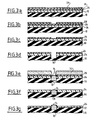
- FIGS. 3a to 3g schematically illustrate the main steps of a method of manufacturing a connector according to the invention
- FIGS. 4a to 4e schematically illustrate the main steps of a variant of this method.
- FIGS. 1 and 2 in which two possible embodiments of a connector according to the invention have been shown diagrammatically.
- the connector of FIG. 1 comprises a support 10 of elastomeric material, which may have a thickness of the order of 2 mm for example, on a face 12 of which electrically conductive lines 14 are formed, connecting two by two of the pads of contact 16, 18, some of which are formed along the edges of the support 10 and the others along the sides of a location of a hybrid circuit or of an integrated circuit.
- the electrically conductive lines 14 can have a width as small as a micrometer and a thickness of the order of a few micrometers.
- the width of the lines 14 can have any desired value depending on the intended use, for example a width of 5, 10, 25, 50 or 100 micrometers.
- electrically conductive lines 14 are formed by solid and continuous metallic conductors, for example of copper, aluminum, silver or gold, they have a very high conductivity.
- the connector according to the invention also comprises a support 10 made of elastomeric material, on one face 12 of which are formed series of electrically conductive lines 14 intended to connect together conductors 20, 22 shown in dotted lines, some of which are formed on a test card for example, and the others of which are input / output conductors of a hybrid circuit or an integrated circuit.
- electrically conductive lines 14 have a width which can be much less than that of the conductors 20, 22, it is possible to provide several lines 14 per pair of conductors 20, 22 and thus make redundant connections between these conductors, which allows a easier positioning of the connector on the components to be connected. In addition, redundant connections are a guarantee of establishing the desired electrical connections.
- the support 10 of elastomeric material may be made of fluorinated rubber, not transparent, or of silicone-based elastomer (transparent) to facilitate the precise positioning of the connector.
- FIGS. 3a to 3g schematically represent the essential steps of a method of manufacturing a connector according to the invention.
- the reference 10 designates, as in FIGS. 1 and 2, the support of elastomeric material, the face 12 of which is covered with a thin intermediate layer 24 of polymeric material (for example of transparent epoxy resin).
- This layer 24 is itself covered with a thin layer 26 of peelable material (commonly called lift-off layer) such as polysiloxane for example.
- the support 10 of elastomeric material may have a thickness of approximately 2 mm, while the intermediate layer 24 has a thickness of approximately 2 to 3 ⁇ m, the layer 26 of peelable material a thickness of approximately 0.3 to 0.5 ⁇ m, and the layer 28 of photo-sensitive resin a thickness of 1 to 1.5 ⁇ m.
- the first step of the process according to the invention consists in subjecting this layer 28 of photo-sensitive resin to sunshine, by exposure to appropriate light radiation, for example ultraviolet radiation, through a mask defining the network of electrically conductive lines 14 to be formed on the face 12 of the support 10. This exposure of the photo-sensitive resin is followed by a development operation of the resin, to arrive at the structure shown in FIG. 3b.
- appropriate light radiation for example ultraviolet radiation
- the method according to the invention then consists in etching the network of electrically conductive lines 14 in the layer 26 of peelable material (FIG. 3c) by means of a sulfur hexafluoride plasma (SF6), then in the intermediate layer 24 and the support 10 (FIG. 3d) by means of an oxygen-rich plasma.
- SF6 sulfur hexafluoride plasma
- This etching makes it possible to form grooves or channels 30 in the face 12 of the support 10, in which the electrically conductive lines 14 will be partially buried.
- the following steps of the method according to the invention consist (FIG. 3e) of depositing a thin layer 32 of the metal chosen on the support thus prepared, that is to say inside the grooves or channels 30 and on the layer 26 of removable material.
- the thickness of the metal layer 32 is for example greater than or equal to approximately 5 ⁇ m, so as to fill the channels or grooves 30 over a height corresponding roughly to the level of the upper face of the intermediate layer 24.
- the metal is deposited by any suitable technique, for example by evaporation, or by spraying, or else by spraying in a thin layer with thickening of the layer by electro-chemical growth, or again by chemical vapor deposition.
- the elastomeric material of the support 10 and the polymeric material of the intermediate layer 24 are chosen so as to withstand the temperatures of deposition of the metal, that is to say at temperatures of the order of 150 to 250 ° C.
- the next step in the process is shown in FIG. 3f and consists in removing the layer 26 of peelable material, as well as the layer of metal 32 which covers it. This can be done mechanically (soaking in liquid nitrogen, causing delamination of layer 26 by differential thermal expansion between this layer on the one hand, and the intermediate layer 24 and the support 10 on the other hand) or chemically (using a dilute hydrofluoric acid solution which attacks the material of layer 26).
- a limited chemical etching of the metal layer can be carried out beforehand to break the thin bridges 34 which connect the metal filling the channels or grooves 30 and the metal layer 32 formed on the layer 26 of peelable material.
- the metal which fills the channels or grooves 30 thus forms the above-mentioned electrically conductive lines 14.
- the height of these lines 14 relative to the face 12 of the support 10 can be adjusted by an additional etching of the intermediate layer 24, making it possible to reduce its thickness, by means of an oxygen-rich plasma.
- all of the material in layer 24 can be removed.
- FIG 4a there is shown a support 10 of elastomeric material, one face 12 of which comprises a network of electrically conductive lines 14, formed of solid and continuous metallic conductors which are buried in the support 10, that is to say that the upper face of the electrically conductive lines 14 is substantially at the level of the upper face 12 of the support 10.
- These electrically conductive lines 14 were formed on the support 10 by means of the method which has just been described with reference to FIGS. 3a to 3g, the height of the channels or grooves 30 receiving the electrically conductive lines 14 and 30 being however calculated so that these lines 14 do not substantially protrude above the support 10.
- the next step of the process consists in depositing on the support 10 a thin layer 36 of polymeric material, for example of the material used for the above-mentioned intermediate thin layer 24.
- This layer 36 may have a thickness of approximately 5 ⁇ m, for example.
- the following stages of the process consist in forming in this layer 36 conductive metal pads which are connected to the electrically conductive lines 14 and which extend over the entire thickness of the layer 36, to lead to the upper face of the latter. .
- This etching of the layer 36 and the deposition of metal forming the pads 38 are carried out by the process steps shown in Figures 3a to 3f.
- the next step consists in depositing a new layer 40 of polymeric material on the aforementioned layer 36 and the bonding pads 38.
- the polymeric material of layer 40 can of course be the same as that of layer 36.
- a final oxygen-rich plasma etching operation makes it possible to reduce the thickness of the layer 40 in order to partially emerge the pads and the lines 42, 44.
- Such a connector is useful in particular when the number of points to be connected is very high and / or when crossing of the interconnection lines is inevitable, for example in the case of circuits in which the contact points are distributed over an entire surface, or on concentric surfaces.
Abstract
Connecteur élastomérique pour circuits intégrés ou analogues, comprenant un support (10) de matière élastomère sur une face (12) duquel est formé un réseau dense de lignes électro-conductrices (14). Des techniques de photogravure et de dépôt de métal sur une couche de matière décollable utilisées pour la fabrication des circuits intégrés, permettent de donner une très faible largeur et une conductivité très élevée aux lignes (14). L'invention s'applique notamment à la connexion et aux tests des circuits intégrés et des circuits hybrides. <IMAGE>
Description
- L'invention concerne un connecteur élastomérique pour circuits intégrés ou analogues, ainsi que le procédé de fabrication d'un tel connecteur.
- Il existe déjà des connecteurs électriques pour circuits intégrés ou analogues, qui comprennent un support en matière élastomère sur lequel sont formées des lignes électro-conductrices de faible largeur, permettant d'établir des liaisons électriques entre des conducteurs d'entrée/sortie de circuits intégrés, de circuits hybrides, de circuits de test, d'alimentation, de commande, etc... Il suffit pour cela que ces connecteurs soient positionnés correctement sur ou entre les circuits à réunir, et que leurs lignes conductrices soient appliquées à pression sur les conducteurs d'entrée/sortie de ces circuits.
- Ces connecteurs présentent un certain nombre d'avantages par rapport à des connecteurs classiques: ils offrent une grande densité de lignes conductrices par unité de longueur, ils peuvent être utilisés dans une large gamme de températures, ils résistent aux chocs et aux vibrations, ils peuvent être montés et démontés un très grand nombre de fois sans détérioration, et ils résistent à de nombreux agents chimiques (les élastomères à base de silicone sont résistants en particulier à l'oxygène, à l'ozone et aux rayons ultraviolets). La nature souple du support en élastomère permet également de relier, moyennant une faible flexion de ce support, des circuits qui ne sont pas exactement au même niveau.
- Les connecteurs connus de ce type présentent cependant quelques inconvénients :
- lorsque les lignes électro-conductrices sont formées par diffusion de carbone ou d'argent dans l'élastomère du support, elles ont une conductivité limitée, et une largeur d'au moins 25 micromètres;
- lorsque ces lignes électro-conductrices sont réalisées par laminage d'une grille conductrice (cuivre, or, etc...) sur le support en élastomère, elles ont une bonne conductivité, mais leur largeur est d'au moins 100 micromètres;
- ils ne présentent qu'un seul niveau de lignes conductrices;
- leurs procédés de fabrication peuvent être relativement complexes et onéreux, notamment lorsque ces connecteurs sont constitués d'un empilage de couches minces alternées respectivement conductrices et isolantes, qui peuvent avoir chacune une épaisseur de l'ordre de 50 micromètres.
- L'invention a notamment pour but de pallier ces divers inconvénients des connecteurs antérieurs connus.
- Elle a pour objet un connecteur électrique du type précité, comprenant un support en élastomère sur lequel sont formées des lignes électro-conductrices de faible largeur, dans lequel les lignes peuvent avoir une excellente conductivité électrique, avec des largeurs qui peuvent être réduites jusqu'au micromètre.
- L'invention a encore pour objet un connecteur de ce type, qui présente des niveaux différents superposés de lignes électro-conductrices.
- L'invention a également pour objet un connecteur de ce type, qui puisse être fabriqué par un procédé relativement simple et peu coûteux, faisant appel à des techniques éprouvées utilisées jusqu'à présent en microélectronique pour la fabrication de circuits intégrés et de circuits hybrides par exemple.
- L'invention propose, à cet effet, un connecteur élastomérique pour circuits intégrés ou analogues, comprenant un support de matière élastomère sur lequel sont formées des lignes électro-conductrices de faible largeur, dont les extrémités sont destinées à être reliées par contact à pression à des conducteurs d'entrée et de sortie desdits circuits intégrés ou analogues, caractérisé en ce que ces lignes électro-conductrices sont des conducteurs métalliques pleins et continus, partiellement enterrés dans le support de matière élastomère et ayant des largeurs minimales de l'ordre du micromètre.
- Les épaisseurs minimales de ces lignes électro-conductrices sont de quelques micromètres.
- On peut donc obtenir un réseau extrêmement dense de lignes électro-conductrices, ayant une très faible résistivité du fait qu'elles sont constituées par des conducteurs métalliques pleins et continus tels que du cuivre ou de l'aluminium. Les connecteurs selon l'invention sont donc particulièrement bien adaptés à réaliser des ensembles de liaisons sur des circuits hybrides portant plusieurs circuits intégrés à grand nombre de conducteurs d'entrée/sortie.
- Avantageusement, la matière élastomère du support est transparente, ce qui facilite un positionnement précis du connecteur par rapport à un circuit intégré ou à un circuit hybride.
- Selon une autre caractéristique de l'invention, le connecteur comprend au moins deux niveaux superposés de lignes électro-conductrices, le niveau supérieur étant séparé du niveau inférieur par une épaisseur d'une matière polymère diélectrique, et les lignes électro-conductrices du niveau inférieur étant reliées à des lignes ou plages électro-conductrices du niveau supérieur par des plots de métal électro-conducteur traversant ladite épaisseur de matière polymère.
- Cette superposition de niveaux de lignes électro-conductrices permet d'augmenter encore la densité des connexions sur le connecteur selon l'invention.
- Bien entendu, la matière polymère interposée entre deux niveaux peut elle aussi être transparente, comme la matière élastomère du support, pour faciliter le positionnement du connecteur selon l'invention.
- L'invention propose également un procédé de fabrication d'un connecteur de ce type, caractérisé en ce qu'il consiste à déposer sur une face du support une couche mince de matière décollable telle que du polysiloxanne, à former des canaux ou rainures par photogravure dans cette couche mince et dans la face sous-jacente du support, à déposer une couche mince de métal électroconducteur sur cette couche de matière décollable et dans les canaux ou rainures précités du support, puis à enlever du support ladite couche de matière décollable avec la couche de métal qui la recouvre, pour ne laisser le métal que dans les canaux ou rainures précités du support.
- Le procédé selon l'invention permet de fixer avec précision les dimensions des lignes conductrices, aussi bien en largeur qu'en épaisseur, et de leur donner des dimensions très faibles si nécessaire, grâce à des techniques éprouvées appliquées jusque là à la fabrication de circuits électroniques intégrés.
- Le procédé selon l'invention est donc fiable, précis et peu coûteux dans la mesure où il peut être exécuté au moyen d'installations existantes.
- Plus précisément, le procédé selon l'invention consiste à déposer sur la couche de matière décollable une couche de résine photo-sensible, à exposer cette couche de résine à un rayonnement lumineux de nature appropriée à travers un masque, à développer ladite couche de résine, puis à graver ladite couche décollable et ensuite la face du support avant de déposer la couche mince de métal électro-conducteur.
- Selon une autre caractéristique de l'invention, le procédé consiste à déposer initialement sur ladite face du support une couche mince intermédiaire de matière polymère, sur laquelle on dépose ensuite la couche mince de matière décollable, puis à graver cette couche mince intermédiaire en même temps que ladite face du support.
- La présence de cette couche mince intermédiaire de matière polymère permet notamment de régler la hauteur des lignes conductrices par rapport à la face précitée du support de la matière élastomère.
- On peut en effet, après dépôt de la couche de métal et enlèvement de la couche de matière décollable, soumettre cette couche intermédiaire à une opération supplémentaire de gravure pour réduire son épaisseur et régler ainsi la hauteur des lignes conductrices par rapport à la face précitée du support.
- Selon encore une autre caractéristique de l'invention, le procédé consiste ensuite à recouvrir la face du support sur laquelle sont formées les lignes électro-conductrices, par une couche mince de matière polymère, à former de la façon précitée par gravure et dépôt de métal, des plots électro-conducteurs traversant cette couche mince et reliés aux lignes électro-conductrices précitées, à déposer ensuite une nouvelle couche mince de matière polymère, et à former dans celle-ci par gravure et dépôt de métal de la façon précitée, une nouvelle série de lignes et de plages électro-conductrices, dont certaines sont reliées aux plots précités.
- On réalise ainsi, de façon simple, un connecteur à deux niveaux de lignes électro-conductrices. En répétant les opérations précitées, on obtient un connecteur à plusieurs niveaux superposés de lignes électro-conductrices.
- L'invention sera mieux comprise et d'autres caractéristiques, détails et avantages de celle-ci apparaîtront plus clairement à la lecture de la description qui suit, faite à titre d'exemple en référence aux dessins annexés dans lesquels :
- la figure 1 est une vue schématique partielle d'un connecteur selon l'invention ;
- la figure 2 est une vue schématique partielle d'une variante de réalisation de ce connecteur ;
- les figures 3a à 3g illustrent schématiquement les principales étapes d'un procédé de fabrication d'un connecteur selon l'invention ;
- les figures 4a à 4e illustrent schématiquement les principales étapes d'une variante de ce procédé.
- On se réfère d'abord aux figures 1 et 2, dans lesquelles on a représenté schématiquement deux formes de réalisation possible d'un connecteur selon l'invention.
- Le connecteur de la figure 1 comprend un support 10 de matière élastomère, pouvant avoir une épaisseur de l'ordre de 2 mm par exemple, sur une face 12 duquel sont formées des lignes électro-conductrices 14 reliant entre elles deux à deux des plages de contact 16, 18 dont les unes sont formées le long des bords du support 10 et les autres le long des côtés d'un emplacement d'un circuit hybride ou d'un circuit intégré.
- Selon l'invention, les lignes électro-conductrices 14 peuvent avoir une largeur aussi faible qu'un micromètre et une épaisseur de l'ordre de quelques micromètres. En pratique, la largeur des lignes 14 peut avoir toute valeur souhaitée en fonction de l'utilisation envisagée, par exemple une largeur de 5, 10, 25, 50 ou 100 micromètres.
- Comme ces lignes électro-conductrices 14 sont formées par des conducteurs métalliques pleins et continus, par exemple de cuivre, d'aluminium, d'argent ou d'or, elles ont une conductivité très élevée.
- Le connecteur selon l'invention, représenté schématiquement en figure 2, comprend lui aussi un support 10 en matière élastomère, sur une face 12 duquel sont formées des séries de lignes 14 électro-conductrices destinées à relier entre eux des conducteurs 20, 22 représentés en pointillés, dont les uns sont formés sur une carte de test par exemple, et dont les autres sont des conducteurs d'entrée/sortie d'un circuit hybride ou d'un circuit intégré.
- Comme les lignes électro-conductrices 14 ont une largeur qui peut être très inférieure à celle des conducteurs 20, 22, on peut prévoir plusieurs lignes 14 par couple de conducteurs 20, 22 et réaliser ainsi des connexions redondantes entre ces conducteurs, ce qui permet un positionnement plus facile du connecteur sur les composants à relier. En outre, la redondance des connexions est une garantie d'établissement des liaisons électriques voulues.
- Le support 10 de matière élastomère peut être en caoutchouc fluoré, non transparent, ou en élastomère à base de silicone (transparent) pour faciliter le positionnement précis du connecteur.
- On se réfèrera maintenant aux figures 3a à 3g, qui représentent schématiquement les étapes essentielles d'un procédé de fabrication d'un connecteur selon l'invention.
- En figure 3a, la référence 10 désigne, comme dans les figures 1 et 2, le support de matière élastomère, dont la face 12 est recouverte d'une couche mince intermédiaire 24 de matière polymère (par exemple de résine époxyde transparente). Cette couche 24 est elle-même recouverte d'une couche mince 26 de matière décollable (communément appelée couche de lift-off) tel que du polysiloxanne par exemple.
- Sur cette couche 26 est enfin déposée une couche mince 28 d'une résine photo-sensible.
- Le support 10 de matière élastomère peut avoir une épaisseur de 2 mm environ, tandis que la couche intermédiaire 24 a une épaisseur de 2 à 3 µm environ, la couche 26 de matière décollable une épaisseur de 0,3 à 0,5 µm environ, et la couche 28 de résine photo-sensible une épaisseur de 1 à 1,5 µm.
- La première étape du procédé selon l'invention consiste à soumettre cette couche 28 de résine photo-sensible à une insolation, par exposition à un rayonnement lumineux approprié, par exemple un rayonnement ultraviolet, à travers un masque définissant le réseau des lignes électro-conductrices 14 à former sur la face 12 du support 10. Cette insolation de la résine photo-sensible est suivie d'une opération de développement de la résine, pour arriver à la structure représentée en figure 3b.
- Le procédé selon l'invention consiste ensuite à graver le réseau de lignes électro-conductrices 14 dans la couche 26 de matière décollable (figure 3c) au moyen d'un plasma d'hexafluorure de soufre (SF6), puis dans la couche intermédiaire 24 et le support 10 (figure 3d) au moyen d'un plasma riche en oxygène.
- Cette gravure permet de former des rainures ou canaux 30 dans la face 12 du support 10, dans lesquels seront enterrées partiellement les lignes électro-conductrices 14.
- Les étapes suivantes du procédé selon l'invention consistent (figure 3e) à déposer une couche mince 32 du métal choisi sur le support ainsi préparé, c'est-à-dire à l'intérieur des rainures ou canaux 30 et sur la couche 26 de matière décollable. L'épaisseur de la couche de métal 32 est par exemple supérieure ou égale à 5 µm environ, de façon à remplir les canaux ou rainures 30 sur une hauteur correspondant à peu près au niveau de la face supérieure de la couche intermédiaire 24.
- Le métal est déposé par toute technique appropriée, par exemple par évaporation, ou par pulvérisation, ou encore par pulvérisation en couche mince avec épaississement de la couche par croissance électro-chimique, soit encore par dépôt de vapeur chimique (Chemical Vapor Déposition).
- Bien entendu, la matière élastomère du support 10 et la matière polymère de la couche intermédiaire 24 sont choisies de manière à résister aux températures de dépôt du métal, c'est-à-dire à des températures de l'ordre de 150 à 250°C.
- L'étape suivante du procédé est représentée en figure 3f et consiste à enlever la couche 26 de matière décollable, ainsi que la couche de métal 32 qui la recouvre. On peut procéder pour cela par voie mécanique (trempage dans de l'azote liquide, provoquant un délaminage de la couche 26 par dilatation thermique différentielle entre cette couche d'une part, et la couche intermédiaire 24 et le support 10 d'autre part) ou par voie chimique ( au moyen d'une solution d'acide fluorhydrique diluée qui attaque la matière de la couche 26).
- Eventuellement, on peut effectuer au préalable une gravure chimique limitée de la couche de métal, pour rompre les ponts 34 de faible épaisseur qui relient le métal remplissant les canaux ou rainures 30 et la couche de métal 32 formée sur la couche 26 de matière décollable.
- Le métal qui remplit les canaux ou rainures 30 forme ainsi les lignes électro-conductrices 14 précitées.
- La hauteur de ces lignes 14 par rapport à la face 12 du support 10 peut être réglée par une gravure supplémentaire de la couche intermédiaire 24, permettant de réduire son épaisseur, au moyen d'un plasma riche en oxygène. Eventuellement, toute la matière de la couche 24 peut être éliminée.
- Le procédé représenté dans les figures 3d à 3g permet donc d'obtenir un connecteur tel que celui représenté en figure 1 ou en figure 2, à un seul niveau de lignes électro-conductrices. On comprend cependant qu'en répétant ce procédé, on peut obtenir un connecteur à plusieurs niveaux superposés de lignes conductrices.
- On peut pour cela procéder de la façon représentée schématiquement dans les figures 4a à 4e.
- En figure 4a, on a représenté un support 10 de matière élastomère, dont une face 12 comprend un réseau de lignes électro-conductrices 14, formées de conducteurs métalliques pleins et continus qui sont enterrés dans le support 10, c'est-à-dire que la face supérieure des lignes électro-conductrices 14 est sensiblement au niveau de la face supérieure 12 du support 10.
- Ces lignes électro-conductrices 14 ont été formées sur le support 10 au moyen du procédé qui vient d'être décrit en référence aux figures 3a à 3g, la hauteur des canaux ou rainures 30 recevant les lignes électro-conductrices 14 et 30 étant toutefois calculée pour que ces lignes 14 ne fassent sensiblement pas saillie au-dessus du support 10.
- L'étape suivante du procédé, représentée en figure 4b, consiste à déposer sur le support 10 une couche mince 36 de matière polymère, par exemple de la matière utilisée pour la couche mince intermédiaire 24 précitée. Cette couche 36 peut avoir une épaisseur de 5 µm environ, par exemple. Les étapes suivantes du procédé consistent à former dans cette couche 36 des plots métalliques conducteurs qui sont reliés aux lignes électro-conductrices 14 et qui s'étendent sur toute l'épaisseur de la couche 36, pour déboucher sur la face supérieure de celle-ci. Cette gravure de la couche 36 et le dépôt de métal formant les plots 38 sont réalisés par les étapes de procédé représentées en figures 3a à 3f.
- L'étape suivante, représentée en figure 4d, consiste à déposer une nouvelle couche 40 de matière polymère sur la couche 36 précitée et les plots de liaison 38. La matière polymère de la couche 40 peut bien entendu être la même que celle de la couche 36.
- On répète ensuite les opérations précitées de gravure et de dépôt de métal pour former dans cette couche 40, d'une part des lignes ou plages de contact 42 qui sont reliées aux plots de contact 38 précités, et d'autre part un autre réseau de lignes électro-conductrices 44 dont au moins certaines vont croiser les lignes 14 du niveau inférieur, tout en étant séparées de celles-ci par la couche de matière polymère 36.
- Une opération finale de gravure au plasma riche en oxygène permet de réduire l'épaisseur de la couche 40 pour faire émerger partiellement les plages et les lignes 42, 44.
- On obtient ainsi un connecteur électrique à deux niveaux de lignes conductrices 14, 44.
- En répétant les étapes des figures 4b à 4e, on peut bien entendu réaliser un connecteur à plusieurs niveaux superposés de lignes conductrices qui se croisent.
- Un tel connecteur est utile notamment lorsque le nombre de points à relier est très élevé et/ou lorsqu'un croisement des lignes d'interconnexion est inévitable, par exemple dans le cas de circuits dont les points de contact sont distribués sur une surface entière, ou sur des surfaces concentriques.
- De façon générale, les avantages de l'invention sont les suivants :
- les lignes électro-conductrices de connexion peuvent être très fines (largeur supérieure ou égale à 1 µm) avec un pas très faible (supérieur ou égal à 5 ou 10 µm)
- ces lignes électro-conductrices ont une conductivité très élevée
- on peut former plusieurs niveaux superposés de connexions
- le procédé de fabrication est fiable et utilise des techniques et des moyens éprouvés dans la fabrication des circuit intégrés
- il est en général plus rapide et moins coûteux que les procédés de fabrication des connecteurs comparables de la technique antérieure.
- le connecteur selon l'invention est utilisable aussi bien pour des connexions à des circuits à grand nombre d'entrées/sorties, que pour des tests de ces circuits, les contacts entre les conducteurs du connecteur et ceux des circuits étant établis par pression mécanique.
Claims (11)
- Connecteur élastomérique pour circuits intégrés ou analogues, comprenant un support (10) de matière élastomère sur lequel sont formées des lignes électro-conductrices (14) de faible largeur, dont les extrémités sont destinées à être reliées par contact à pression à des conducteurs d'entrée et de sortie desdits circuits intégrés ou analogues, caractérisé en ce que ces lignes électro-conductrices sont des conducteurs métalliques pleins et continus partiellement enterrés dans le support (10) de matière élastomère et ayant des largeurs minimales de l'ordre du micromètre.
- Connecteur selon la revendication 1, caractérisé en ce que les épaisseurs minimales des lignes électro-conductrices sont de quelques micromètres.
- Connecteur selon la revendication 1 ou 2, caractérisé en ce que le pas minimal des lignes électro-conductrices (14) est de quelques micromètres.
- Connecteur selon l'une des revendications précédentes, caractérisé en ce que la matière élastomère du support (10) est transparente.
- Connecteur selon l'une des revendications précédentes, caractérisé en ce qu'il comprend au moins deux niveaux superposés de lignes conductrices (14, 44), le niveau supérieur étant séparé du niveau inférieur par une épaisseur (36) d'une matière polymère diélectrique, les lignes électro-conductrices (14) du niveau inférieur étant reliées à des lignes ou plages électro-conductrices (42) du niveau supérieur par des plots (38) de métal électro-conducteur traversant ladite épaisseur (36) de la matière polymère.
- Connecteur selon la revendication 5, caractérisé en ce que ladite matière polymère (36) est transparente.
- Procédé de fabrication d'un connecteur élastomérique pour circuits intégrés ou analogues, comprenant un support (10) de matière élastomère sur lequel sont formées des lignes électro-conductrices (14) de faible largeur, caractérisé en ce qu'il consiste à déposer sur une face (12) du support une couche mince (26) de matière décollable telle que du polysiloxanne, à former des canaux ou rainures (30) par photogravure dans cette couche mince (26) et dans la face (12) sous-jacente du support, à déposer une couche mince (32) de métal électro-conducteur sur cette couche de matière décollable (26) et dans les canaux ou rainures précités du support (10), puis en enlever du support ladite couche de matière décollable (26) avec la couche de métal qui la recouvre, pour ne laisser le métal que dans les canaux ou rainures (30) précités du support.
- Procédé selon la revendication 7, caractérisé en ce que, pour la photogravure, il consiste à déposer sur la couche (26) de matière décollable une couche (28) de résine photosensible, à exposer cette couche de résine à un rayonnement lumineux de nature appropriée à travers un masque, à développer ladite couche de résine (28), puis à graver ladite couche (26) de matière décollable et ensuite la face (12) du support (10) avant de déposer la couche mince (32) de métal électro-conducteur.
- Procédé selon la revendication 7 ou 8, caractérisé en ce qu'il consiste à déposer initialement sur la face (12) du support une couche mince intermédiaire (24) de matière polymère sur laquelle on dépose ensuite la couche mince de matière décollable (26), puis à graver cette couche mince intermédiaire (24) en même temps que la face (12) du support (10).
- Procédé selon la revendication 9, caractérisé en ce que, après dépôt de la couche (32) de métal et enlèvement de la couche de matière décollable (26), on soumet ladite couche intermédiaire (24) à une opération supplémentaire de gravure pour réduire son épaisseur.
- Procédé selon l'une des revendications 7 à 10, caractérisé en ce qu'il consiste ensuite à recouvrir ladite face du support (10) sur laquelle sont formées les lignes électro-conductrices (14), d'une couche mince (36) de matière polymère, à former, de la façon précitée par gravure et dépôt de métal, des plots électro-conducteurs (38) traversant cette couche mince et reliés aux lignes électro-conductrices (14) précitées, à déposer ensuite une nouvelle couche mince (40) de matière polymère, et à former dans celle-ci, par gravure et dépôt de métal de la façon précitée, une nouvelle série de lignes et de plages électro-conductrices (42, 44) dont certaines sont reliées aux plots précités (38).
Applications Claiming Priority (2)
| Application Number | Priority Date | Filing Date | Title |
|---|---|---|---|
| FR9002781 | 1990-03-06 | ||
| FR9002781A FR2659495B1 (fr) | 1990-03-06 | 1990-03-06 | Connecteur elastomerique pour circuits integres ou analogues, et son procede de fabrication. |
Publications (1)
| Publication Number | Publication Date |
|---|---|
| EP0446112A1 true EP0446112A1 (fr) | 1991-09-11 |
Family
ID=9394406
Family Applications (1)
| Application Number | Title | Priority Date | Filing Date |
|---|---|---|---|
| EP91400573A Withdrawn EP0446112A1 (fr) | 1990-03-06 | 1991-03-01 | Connecteur élastomérique pour circuits intégrés ou analogues, et son procédé de fabrication |
Country Status (4)
| Country | Link |
|---|---|
| US (1) | US5152868A (fr) |
| EP (1) | EP0446112A1 (fr) |
| JP (1) | JPH07122322A (fr) |
| FR (1) | FR2659495B1 (fr) |
Cited By (1)
| Publication number | Priority date | Publication date | Assignee | Title |
|---|---|---|---|---|
| US6410859B1 (en) * | 1995-07-10 | 2002-06-25 | Micron Technology, Inc. | Electrical assembly for semiconductor dice |
Families Citing this family (9)
| Publication number | Priority date | Publication date | Assignee | Title |
|---|---|---|---|---|
| JPH045844A (ja) * | 1990-04-23 | 1992-01-09 | Nippon Mektron Ltd | Ic搭載用多層回路基板及びその製造法 |
| DE69233684D1 (de) * | 1991-02-22 | 2007-04-12 | Canon Kk | Elektrischer Verbindungskörper und Herstellungsverfahren dafür |
| EP0526133B1 (fr) * | 1991-07-26 | 1997-03-19 | Nec Corporation | Plaquette de circuits multicouche en polyimide et son procédé de fabrication |
| US5244534A (en) * | 1992-01-24 | 1993-09-14 | Micron Technology, Inc. | Two-step chemical mechanical polishing process for producing flush and protruding tungsten plugs |
| US5329695A (en) * | 1992-09-01 | 1994-07-19 | Rogers Corporation | Method of manufacturing a multilayer circuit board |
| US5890915A (en) * | 1996-05-17 | 1999-04-06 | Minnesota Mining And Manufacturing Company | Electrical and thermal conducting structure with resilient conducting paths |
| US6403226B1 (en) | 1996-05-17 | 2002-06-11 | 3M Innovative Properties Company | Electronic assemblies with elastomeric members made from cured, room temperature curable silicone compositions having improved stress relaxation resistance |
| DE10332333B4 (de) * | 2003-07-16 | 2006-08-03 | Siemens Ag | Detektormodul |
| JP2012164388A (ja) * | 2011-02-07 | 2012-08-30 | Showa Denko Kk | 磁気記録媒体の製造方法及び磁気記録再生装置 |
Citations (5)
| Publication number | Priority date | Publication date | Assignee | Title |
|---|---|---|---|---|
| EP0072673A2 (fr) * | 1981-08-13 | 1983-02-23 | Minnesota Mining And Manufacturing Company | Film support à conducteurs pour l'interconnexion électrique entre des composants électroniques et un circuit externe |
| DE3616493A1 (de) * | 1985-05-20 | 1986-11-20 | Tektronix, Inc., Beaverton, Oreg. | Verfahren zum packen von chips fuer integrierte schaltungen und integrierte schaltungspackungen |
| US4681654A (en) * | 1986-05-21 | 1987-07-21 | International Business Machines Corporation | Flexible film semiconductor chip carrier |
| EP0310357A2 (fr) * | 1987-09-29 | 1989-04-05 | Microelectronics and Computer Technology Corporation | Circuit adaptable |
| WO1989012911A1 (fr) * | 1988-06-24 | 1989-12-28 | Unistructure, Inc. | Cadre de montage protege et procede de fabrication de cadres de montage |
Family Cites Families (5)
| Publication number | Priority date | Publication date | Assignee | Title |
|---|---|---|---|---|
| US3711625A (en) * | 1971-03-31 | 1973-01-16 | Microsystems Int Ltd | Plastic support means for lead frame ends |
| US4400234A (en) * | 1975-11-13 | 1983-08-23 | Tektronix, Inc. | Method of manufacturing electrical connector |
| US4606787A (en) * | 1982-03-04 | 1986-08-19 | Etd Technology, Inc. | Method and apparatus for manufacturing multi layer printed circuit boards |
| US4650545A (en) * | 1985-02-19 | 1987-03-17 | Tektronix, Inc. | Polyimide embedded conductor process |
| US4964948A (en) * | 1985-04-16 | 1990-10-23 | Protocad, Inc. | Printed circuit board through hole technique |
-
1990
- 1990-03-06 FR FR9002781A patent/FR2659495B1/fr not_active Expired - Fee Related
-
1991
- 1991-03-01 EP EP91400573A patent/EP0446112A1/fr not_active Withdrawn
- 1991-03-04 US US07/664,342 patent/US5152868A/en not_active Expired - Fee Related
- 1991-03-05 JP JP3063991A patent/JPH07122322A/ja active Pending
Patent Citations (5)
| Publication number | Priority date | Publication date | Assignee | Title |
|---|---|---|---|---|
| EP0072673A2 (fr) * | 1981-08-13 | 1983-02-23 | Minnesota Mining And Manufacturing Company | Film support à conducteurs pour l'interconnexion électrique entre des composants électroniques et un circuit externe |
| DE3616493A1 (de) * | 1985-05-20 | 1986-11-20 | Tektronix, Inc., Beaverton, Oreg. | Verfahren zum packen von chips fuer integrierte schaltungen und integrierte schaltungspackungen |
| US4681654A (en) * | 1986-05-21 | 1987-07-21 | International Business Machines Corporation | Flexible film semiconductor chip carrier |
| EP0310357A2 (fr) * | 1987-09-29 | 1989-04-05 | Microelectronics and Computer Technology Corporation | Circuit adaptable |
| WO1989012911A1 (fr) * | 1988-06-24 | 1989-12-28 | Unistructure, Inc. | Cadre de montage protege et procede de fabrication de cadres de montage |
Cited By (1)
| Publication number | Priority date | Publication date | Assignee | Title |
|---|---|---|---|---|
| US6410859B1 (en) * | 1995-07-10 | 2002-06-25 | Micron Technology, Inc. | Electrical assembly for semiconductor dice |
Also Published As
| Publication number | Publication date |
|---|---|
| JPH07122322A (ja) | 1995-05-12 |
| FR2659495B1 (fr) | 1997-01-24 |
| FR2659495A1 (fr) | 1991-09-13 |
| US5152868A (en) | 1992-10-06 |
Similar Documents
| Publication | Publication Date | Title |
|---|---|---|
| EP0222668B1 (fr) | Procédé de fabrication par gravure en escalier d'un transistor en couches minces à grille auto-alignée par rapport au drain et à la source de celui-ci et transistor obtenu par ce procédé | |
| EP0596456B1 (fr) | Procédé de fabrication de transducteurs capacitifs intégrés | |
| EP0975979B1 (fr) | Procede de fabrication d'une carte a pointes de contact multiple pour le test des puces semiconductrices | |
| EP0446112A1 (fr) | Connecteur élastomérique pour circuits intégrés ou analogues, et son procédé de fabrication | |
| EP1421623A1 (fr) | Capteur d'image couleur a colorimetrie amelioree et procede de fabrication | |
| EP2577723B1 (fr) | Procede de lithographie pour la realisation de reseaux de conducteurs relies par des vias | |
| WO2005086232A1 (fr) | Dispositif microelectronique d'interconnexion a tiges conductrices localisees | |
| EP1421624B1 (fr) | Procede de fabrication de capteur d'image couleur avec ouvertures de contact creusees avant amincissement | |
| EP0372644A1 (fr) | Procédé de réalisation d'un circuit intégré incluant des étapes pour réaliser des interconnexions entre des motifs réalisés à des niveaux différents | |
| EP0411985A1 (fr) | Procédé de formation du réseau multicouche d'une carte de connexion d'au moins un circuit intégré de haute densité | |
| FR2502399A1 (fr) | Dispositif a semi-conducteurs comportant un contact rapporte a faible resistance | |
| EP1700343A1 (fr) | Procede de fabrication de puces electroniques en silicium aminci | |
| FR2829290A1 (fr) | Capteur d'image couleur sur substrat transparent et procede de fabrication | |
| FR2779274A1 (fr) | Circuit integre avec couche d'arret et procede de fabrication associe | |
| EP0058577B1 (fr) | Dispositif semiconducteur de déviation d'électrons du type "à transport balistique", et procédé de fabrication d'un tel dispositif | |
| EP0059206B1 (fr) | Circuit imprime et son procede de fabrication | |
| EP2920811B1 (fr) | Interposeur en graphene et procede de fabrication d'un tel interposeur | |
| EP0415806A1 (fr) | Procédé de dépôt d'une couche isolante sur une couche conductrice du réseau multicouche d'une carte de connexion de circuit intégré de haute densité, et carte en résultant | |
| EP0163581A1 (fr) | Procédé de réalisation d'un dispositif de raccordement électrique entre deux cartes de circuits imprimés, dispositif ainsi obtenu, et procédé de raccordement électrique mettant en oeuvre ce dispositif | |
| WO2007113194A1 (fr) | Procédé de réalisation de structures en multicouches à propriétés contrôlées | |
| EP0125968A1 (fr) | Composant semi-conducteur de puissance, et procédé pour sa fabrication | |
| EP0506526A1 (fr) | Module hybride et procédé de réalisation | |
| FR2830978A1 (fr) | Dispositif a capacite electrique variable integree et procede de realisation d'un tel dispositif | |
| FR3076061A1 (fr) | Realisation d'un collecteur de dispositif microelectronique | |
| FR2520179A1 (fr) | Dispositif de commutation en cascade par flexion de fibres optiques pour reseau de transmission d'informations |
Legal Events
| Date | Code | Title | Description |
|---|---|---|---|
| PUAI | Public reference made under article 153(3) epc to a published international application that has entered the european phase |
Free format text: ORIGINAL CODE: 0009012 |
|
| AK | Designated contracting states |
Kind code of ref document: A1 Designated state(s): DE GB |
|
| 17P | Request for examination filed |
Effective date: 19920224 |
|
| 17Q | First examination report despatched |
Effective date: 19950306 |
|
| STAA | Information on the status of an ep patent application or granted ep patent |
Free format text: STATUS: THE APPLICATION IS DEEMED TO BE WITHDRAWN |
|
| 18D | Application deemed to be withdrawn |
Effective date: 19970114 |