EP0456320A2 - Automatic focus control device - Google Patents
Automatic focus control device Download PDFInfo
- Publication number
- EP0456320A2 EP0456320A2 EP91201069A EP91201069A EP0456320A2 EP 0456320 A2 EP0456320 A2 EP 0456320A2 EP 91201069 A EP91201069 A EP 91201069A EP 91201069 A EP91201069 A EP 91201069A EP 0456320 A2 EP0456320 A2 EP 0456320A2
- Authority
- EP
- European Patent Office
- Prior art keywords
- focus control
- circuit
- output
- video signal
- signal
- Prior art date
- Legal status (The legal status is an assumption and is not a legal conclusion. Google has not performed a legal analysis and makes no representation as to the accuracy of the status listed.)
- Granted
Links
Images

Classifications
-
- H—ELECTRICITY
- H04—ELECTRIC COMMUNICATION TECHNIQUE
- H04N—PICTORIAL COMMUNICATION, e.g. TELEVISION
- H04N23/00—Cameras or camera modules comprising electronic image sensors; Control thereof
- H04N23/95—Computational photography systems, e.g. light-field imaging systems
- H04N23/958—Computational photography systems, e.g. light-field imaging systems for extended depth of field imaging
- H04N23/959—Computational photography systems, e.g. light-field imaging systems for extended depth of field imaging by adjusting depth of field during image capture, e.g. maximising or setting range based on scene characteristics
Definitions
- the present invention relates to an automatic focus control device for use in a video camera, an electronic still camera or the like.
- a focus control signal is formed, in general, based on the high-frequency components of a subject which are contained in a video signal thereof.
- the camera lens system is then moved in response to the focus control signal so that an in-focus state of the subject is attained.
- various circuit structures have been proposed for forming such a focus control signal.
- US Patent No. 4,717,959 discloses an automatic focusing device provided with a circuit in which differentiated values of a video signal are accumulated with values of the video signal itself being also accumulated. The accumulated values of the differentiated values are then divided by the accumulated values of the video signal to form a focus control signal.
- an automatic focus control device which comprises a camera lens, an image sensor element for converting optical information of a subject received through the camera lens into a video signal and control means for moving the camera lens in accordance with a focus control signal produced based on the video signal is characterized by comprising: a differentiation circuit for differentiating the video signal to form differentiated values thereof; an accumulator for successively accumulating the differentiated values; a time-measuring circuit for measuring time periods during which the differentiated values exceed a predetermined value; and a divider for dividing an output of the accumulator by an output of the time-measuring circuit; wherein the focus control signal is obtained from an output of the divider.
- a focus control signal which provides a large discrimination between an in-focus state and an out-of-focus state of a subject having less amount of high-frequency components, such as a subject having a white background with vertical black stripes or black dots and a subject having a black background with vertical white stripes or white dots.
- the accumulator may be constructed such that the differentiated values are successively accumulated in response to a clock signal of a predetermined time interval.
- the time-measuring circuit may be constructed with a counter which counts the clock signal during the time when the differentiated values exceed the predetermined value.
- the differentiation circuit may further be constructed comprising a delay circuit for delaying the video signal by a predetermined time interval and a difference forming circuit for forming a difference between the video signal and an output of the delay circuit, so that the differentiated values are obtained at an output terminal of the difference forming circuit.
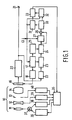
- a camera lens system of a video camera to which an automatic focus control device according to the invention is applied is applied.
- This lens system comprises a front lens group 11, a zoom lens group 12, an iris device 13 and a master lens group 14.
- Optical information of a subject passed through the camera lens system 10 reaches an image-pickup element 16.
- This image-pickup element is comprised, for example, of a charge coupled device (CCD) and is driven by a drive circuit 18 synchronized with an output from a timing generator 17 to convert the optical information into an electric signal complying with a predetermined scanning system.
- the signal from the image-pickup element 16 is supplied through a correlation double sampling circuit 20 to an output terminal 21 and a low-pass filter 22 as a video signal.
- the video signal at the output terminal 21 is supplied to other video signal processing sections (not shown) inside and/or outside this video camera.
- the video signal supplied to the low-pass filter 22 is subjected therein to a filtering for removing its unnecessary frequency components to cause it to represent a luminance signal and is then supplied to an analog-to-digital (A/D) converter 23.
- A/D converter converts the supplied video signal into digital values at a predetermined sampling interval and supplies these values to a gate circuit 24.
- This gate circuit is controlled by a window circuit 25, which has a known structure and is synchronized with another output of the timing generator 17, to output only those portions of the digital video signal which correspond to a selected scanning area (i.e., a window defining the focus control area).
- the video signal passed through the gate circuit 24 is supplied to one input terminal of a difference forming circuit 26 and to an input terminal of a delay circuit 27 for effecting a signal delay of one clock period T based on a clock signal CL which has a predetermined period and is supplied from the timing generator 17.
- the difference forming circuit 26 forms a difference between the output of the gate circuit 24 and that of the delay circuit 27 and outputs the difference in an absolute value. This output of the difference forming circuit 26 is supplied to a noise eliminator 30.
- the noise eliminator 30 supplies the output data of the difference forming circuit 26 to an accumulator 31 as it is and to a counter 32 as an enabling signal when the data is greater than a predetermined value.
- the accumulator 31 accumulates the supplied data, for example, for each picture field in response to respective pulses of the aforesaid clock signal CL and supplies the accumulated data to one input terminal of a divider 33.
- the counter 32 counts the pulses of the clock signal CL when the enabling signal is supplied, which counting operation is performed, for example, for each field.
- the divider 33 divides the resultant accumulated data fed from the accumulator 31 by the count result fed from the counter 32 and outputs the quotient to a microcomputer 35 as evaluation data for the focus control, i.e., as a focus control signal.
- the microcomputer 35 is of the conventional structure and carries out the focus control based on the above focus control signal in a manner as described, for example, in US Patent No. 4,717,959. More specifically, the microcomputer 35 is so arranged as to drive through a motor drive circuit 36 a motor 37 coupled to the front lens group 11 to thereby move the same back and forth along an optical axis thereof. The microcomputer 35 is also arranged to receive information representative of the axial position of the front lens group 11 through a sensor circuit 38. The microcomputer 35 further receives information representative of the position of the zoom lens group 12 and of the degree of opening of the iris device 13 through the sensor circuits 39 and 40, respectively.
- the microcomputer 35 carries out the focus control by driving the motor 37 based on the focus control signal fed from the divider 33 and with reference to other signals, for example, from the above-described sensor circuits so that the front lens group 11 is moved to such a position at which the focus control signal takes the maximum value.
- Fig. 2-(a) shows the picture in the in-focus condition within the focus control window, which picture is of the subject having a black background 51, 51 with a vertical white stripe 52. As described earlier, the width of the vertical stripe 52 corresponds only to one clock period T but is illustrated exaggeratedly.
- Fig. 2-(b) shows the output signal of the gate circuit 24 in the above case, wherein the signal has a "0" level corresponding to the black background 51, 51 and another level, for example, of "3" for one clock period T corresponding to the vertical white stripe.
- Fig. 2-(c) shows the output of the delay circuit 27. As a result, the output of the difference forming circuit 26 has such a waveform as illustrated in Fig.
- Fig. 3-(a) shows the picture within the focus control window 50 which has been obtained by shooting the same subject as in Fig. 2 in an out-of-focus condition, wherein a gray area 53 appears between the black background 51,51 and the vertical white stripe 52 due to the out-of-focusing.
- Fig. 3-(b) shows the output signal of the gate circuit 24 similarly to the showing of Fig. 2-(b), which signal now has in addition to a "0" level corresponding to the black background 51, 51 and a level of "3" corresponding to the vertical white stripe 52 another level, for example, of "1" corresponding to the gray area 53, 53.
- Figs. 3-(c) and 3-(d) show the outputs of the delay circuit 27 and the difference forming circuit 26, respectively.
- the value of the focus control signal produced at the divider 33 in each picture field in this out-of-focus condition can be obtained in the same manner as in the case of Fig. 2:
- the focus control signal fed from the divider 33 thus provides a sufficient discrimination, such as 3 to 1.5, between the in-focus condition and the out-of-focus condition even for such a subject having less high-frequency components as that shown in Figs. 2 and 3.
- Fig. 4-(a) shows the picture within the focus control window 50 which has been obtained by shooting another subject having a black background 60 with a white dot 61 in a in-focus condition.
- the white dot 61 is located on the nth horizontal line and has a diameter of the order of one clock period T, when measured in the horizontal direction, and of the same order of the width of a horizontal line when measured in the vertical direction.
- Fig. 4-(b) shows the output signal of the gate circuit 24 corresponding to nth horizontal line, which signal has a "0" level corresponding to the black background 60 and another level, for example, of "3" corresponding to the white dot 61.
- Fig. 5-(a) shows the picture within the focus control window 50 which has been obtained by shooting the same subject as in Fig. 4 in an out-of-focus condition, wherein gray areas 62 and 62 appear on both sides of the white dot 61 due to the out-of-focusing.
- Fig. 5-(b) shows the output signal of the gate circuit 24, which signal now has in addition to a "0" level corresponding to the black background 60, 60 and a level of "3" corresponding to the white dot 61 another level, for example, of "1" corresponding to the gray area 62, 62.
- the focus control signal fed from the divider 33 provides a sufficient discrimination, such as 3 to 1.5, between the in-focus condition and the out-of-focus condition even for such a subject which has less high-frequency components as that shown in Figs. 4 and 5.
Landscapes
- Engineering & Computer Science (AREA)
- Computing Systems (AREA)
- Theoretical Computer Science (AREA)
- Multimedia (AREA)
- Signal Processing (AREA)
- Automatic Focus Adjustment (AREA)
- Focusing (AREA)
Abstract
Description
- The present invention relates to an automatic focus control device for use in a video camera, an electronic still camera or the like.
- In the conventional automatic focus control device of this type, a focus control signal is formed, in general, based on the high-frequency components of a subject which are contained in a video signal thereof. The camera lens system is then moved in response to the focus control signal so that an in-focus state of the subject is attained. Conventionally, various circuit structures have been proposed for forming such a focus control signal. US Patent No. 4,717,959 discloses an automatic focusing device provided with a circuit in which differentiated values of a video signal are accumulated with values of the video signal itself being also accumulated. The accumulated values of the differentiated values are then divided by the accumulated values of the video signal to form a focus control signal. With such a circuit, however, it is difficult to obtain a focus control signal which has a large discrimination between an in-focus state and an out-of-focus state of a subject having less high-frequency components as a whole. One example of such a subject may be a subject with vertical stripes which have fewer points at which the luminance changes. Consequently, with the conventional automatic focus control device it has been difficult to obtain an accurate in-focus state of a subject which has less high-frequency components.
- It is therefore an object of the present invention to provide an automatic focus control device in which an accurate in-focus state can be obtained even with respect to a subject which has less amount of high-frequency components.
- According to the present invention, an automatic focus control device which comprises a camera lens, an image sensor element for converting optical information of a subject received through the camera lens into a video signal and control means for moving the camera lens in accordance with a focus control signal produced based on the video signal is characterized by comprising:
a differentiation circuit for differentiating the video signal to form differentiated values thereof;
an accumulator for successively accumulating the differentiated values;
a time-measuring circuit for measuring time periods during which the differentiated values exceed a predetermined value;
and
a divider for dividing an output of the accumulator by an output of the time-measuring circuit;
wherein the focus control signal is obtained from an output of the divider. - With the above structure, it is possible to obtain a focus control signal which provides a large discrimination between an in-focus state and an out-of-focus state of a subject having less amount of high-frequency components, such as a subject having a white background with vertical black stripes or black dots and a subject having a black background with vertical white stripes or white dots.
- In an automatic focus control device according to the present invention, the accumulator may be constructed such that the differentiated values are successively accumulated in response to a clock signal of a predetermined time interval. In this case, the time-measuring circuit may be constructed with a counter which counts the clock signal during the time when the differentiated values exceed the predetermined value.
- The differentiation circuit may further be constructed comprising a delay circuit for delaying the video signal by a predetermined time interval and a difference forming circuit for forming a difference between the video signal and an output of the delay circuit, so that the differentiated values are obtained at an output terminal of the difference forming circuit.
- One embodiment of the present invention will now be described by way of example with reference to the accompanying drawings, in which:
- Fig. 1 is a block diagram of an automatic focus control device according to the invention which has been applied to a video camera;
- Figs. 2 and 3 are illustrations for explaining the operation of the embodiment of Fig. 1 with regard to an in-focus state and an out-of-focus state, respectively, of a subject having a black background with a vertical white stripe; and
- Figs. 4 and 5 are illustrations for explaining the operation of the embodiment of Fig. 1 with regard to an in-focus state and an out-of-focus state, respectively, of a subject having a black background with a white dot.
- In Fig. 1, shown at 10 is a camera lens system of a video camera to which an automatic focus control device according to the invention is applied. This lens system comprises a front lens group 11, a zoom lens group 12, an
iris device 13 and amaster lens group 14. - Optical information of a subject passed through the
camera lens system 10 reaches an image-pickup element 16. This image-pickup element is comprised, for example, of a charge coupled device (CCD) and is driven by adrive circuit 18 synchronized with an output from atiming generator 17 to convert the optical information into an electric signal complying with a predetermined scanning system. The signal from the image-pickup element 16 is supplied through a correlationdouble sampling circuit 20 to anoutput terminal 21 and a low-pass filter 22 as a video signal. The video signal at theoutput terminal 21 is supplied to other video signal processing sections (not shown) inside and/or outside this video camera. - The video signal supplied to the low-
pass filter 22 is subjected therein to a filtering for removing its unnecessary frequency components to cause it to represent a luminance signal and is then supplied to an analog-to-digital (A/D)converter 23. This A/D converter converts the supplied video signal into digital values at a predetermined sampling interval and supplies these values to agate circuit 24. This gate circuit is controlled by awindow circuit 25, which has a known structure and is synchronized with another output of thetiming generator 17, to output only those portions of the digital video signal which correspond to a selected scanning area (i.e., a window defining the focus control area). The video signal passed through thegate circuit 24 is supplied to one input terminal of adifference forming circuit 26 and to an input terminal of adelay circuit 27 for effecting a signal delay of one clock period T based on a clock signal CL which has a predetermined period and is supplied from thetiming generator 17. Thedifference forming circuit 26 forms a difference between the output of thegate circuit 24 and that of thedelay circuit 27 and outputs the difference in an absolute value. This output of thedifference forming circuit 26 is supplied to anoise eliminator 30. - The
noise eliminator 30 supplies the output data of thedifference forming circuit 26 to anaccumulator 31 as it is and to acounter 32 as an enabling signal when the data is greater than a predetermined value. Theaccumulator 31 accumulates the supplied data, for example, for each picture field in response to respective pulses of the aforesaid clock signal CL and supplies the accumulated data to one input terminal of adivider 33. Thecounter 32 counts the pulses of the clock signal CL when the enabling signal is supplied, which counting operation is performed, for example, for each field. Thedivider 33 divides the resultant accumulated data fed from theaccumulator 31 by the count result fed from thecounter 32 and outputs the quotient to amicrocomputer 35 as evaluation data for the focus control, i.e., as a focus control signal. - The
microcomputer 35 is of the conventional structure and carries out the focus control based on the above focus control signal in a manner as described, for example, in US Patent No. 4,717,959. More specifically, themicrocomputer 35 is so arranged as to drive through a motor drive circuit 36 amotor 37 coupled to the front lens group 11 to thereby move the same back and forth along an optical axis thereof. Themicrocomputer 35 is also arranged to receive information representative of the axial position of the front lens group 11 through asensor circuit 38. Themicrocomputer 35 further receives information representative of the position of the zoom lens group 12 and of the degree of opening of theiris device 13 through thesensor circuits microcomputer 35 carries out the focus control by driving themotor 37 based on the focus control signal fed from thedivider 33 and with reference to other signals, for example, from the above-described sensor circuits so that the front lens group 11 is moved to such a position at which the focus control signal takes the maximum value. - The operation of this embodiment having the above-described structure will now be described with reference to Figs. 2 to 5.
- For simplicity, description will hereinafter be made only as to each case where the picture of a subject within the focus control window has a black background with a vertical white strip or a black background with a white dot. In this case, it is assumed that the width of the vertical white stripe in the horizontal direction and the diameter of the white dot are each of the order of one clock period T of the clock signal CL. It should be noted that the vertical white stripe and the white dot are illustrated in an exaggerated manner in these figures.
- Fig. 2-(a) shows the picture in the in-focus condition within the focus control window, which picture is of the subject having a
black background white stripe 52. As described earlier, the width of thevertical stripe 52 corresponds only to one clock period T but is illustrated exaggeratedly. Fig. 2-(b) shows the output signal of thegate circuit 24 in the above case, wherein the signal has a "0" level corresponding to theblack background delay circuit 27. As a result, the output of thedifference forming circuit 26 has such a waveform as illustrated in Fig. 2-(d), which waveform indicates that the accumulated values of ak (k = 1, 2, 3, ...) to be obtained at theaccumulator 31 for each horizontal fine will be 3 + 3 = 6. Therefore, if thefocus control window 50 contains m horizontal lines, the accumulated values obtained at theaccumulator 31 in one picture field will be:
On the other hand, the count result at thecounter 32 is 2m. The value of the focus control signal obtained at thedivider 33 in each field is thus:

- Fig. 3-(a) shows the picture within the
focus control window 50 which has been obtained by shooting the same subject as in Fig. 2 in an out-of-focus condition, wherein agray area 53 appears between theblack background white stripe 52 due to the out-of-focusing. Fig. 3-(b) shows the output signal of thegate circuit 24 similarly to the showing of Fig. 2-(b), which signal now has in addition to a "0" level corresponding to theblack background white stripe 52 another level, for example, of "1" corresponding to thegray area delay circuit 27 and thedifference forming circuit 26, respectively. The value of the focus control signal produced at thedivider 33 in each picture field in this out-of-focus condition can be obtained in the same manner as in the case of Fig. 2:
- It will be appreciated that the focus control signal fed from the
divider 33 thus provides a sufficient discrimination, such as 3 to 1.5, between the in-focus condition and the out-of-focus condition even for such a subject having less high-frequency components as that shown in Figs. 2 and 3. - Fig. 4-(a) shows the picture within the
focus control window 50 which has been obtained by shooting another subject having ablack background 60 with awhite dot 61 in a in-focus condition. In that case, it is assumed that thewhite dot 61 is located on the nth horizontal line and has a diameter of the order of one clock period T, when measured in the horizontal direction, and of the same order of the width of a horizontal line when measured in the vertical direction. Fig. 4-(b) shows the output signal of thegate circuit 24 corresponding to nth horizontal line, which signal has a "0" level corresponding to theblack background 60 and another level, for example, of "3" corresponding to thewhite dot 61. Figs. 4-(c) and 4-(d) show the outputs of thedelay circuit 27 and thedifference forming circuit 26, respectively. Therefore, the value of the focus control signal obtained at thedivider 33 in each field is:

- Fig. 5-(a) shows the picture within the
focus control window 50 which has been obtained by shooting the same subject as in Fig. 4 in an out-of-focus condition, whereingray areas white dot 61 due to the out-of-focusing. Fig. 5-(b) shows the output signal of thegate circuit 24, which signal now has in addition to a "0" level corresponding to theblack background white dot 61 another level, for example, of "1" corresponding to thegray area delay circuit 27 and thedifference forming circuit 26, respectively. Therefore, the value of the focus control signal produced at thedivider 33 in each picture field in this out-of-focus condition is:

- It will be appreciated from the above that the focus control signal fed from the
divider 33 provides a sufficient discrimination, such as 3 to 1.5, between the in-focus condition and the out-of-focus condition even for such a subject which has less high-frequency components as that shown in Figs. 4 and 5.
Claims (3)
- An automatic focus control device which comprises a camera lens, an image sensor element for converting optical information of a subject received through the camera lens into a video signal and control means for moving the camera lens in accordance with a focus control signal produced based on the video signal, said automatic focus control device characterized by comprising:
a differentiation circuit for differentiating the video signal to form differentiated values thereof;
an accumulator for successively accumulating said differentiated values;
a time-measuring circuit for measuring time periods during which said differentiated values exceed a predetermined value;
and
a divider for dividing an output of said accumulator by an output of said time-measuring circuit;
wherein the focus control signal is obtained from an output of said divider. - An automatic focus control device according to claim 1, characterized in that said accumulator is so constructed as to successively accumulate the differentiated values in response to clock signals of a predetermined time interval, said time-measuring circuit comprising a counter which counts the clock signals during the time periods when the differentiated values exceed said predetermined value, said divider dividing the output of said accumulator by an output of said counter.
- An automatic focus control device according to claim 1 or claim 2, characterized in that said differentiation circuit comprises a delay circuit for delaying the video signal by a predetermined time period and a difference forming circuit for forming a difference between the video signal and an output of said delay circuit, whereby the differentiated values are obtained at an output terminal of said difference forming circuit.
Applications Claiming Priority (2)
| Application Number | Priority Date | Filing Date | Title |
|---|---|---|---|
| JP122664/90 | 1990-05-11 | ||
| JP2122664A JPH0418872A (en) | 1990-05-11 | 1990-05-11 | Automatic focusing controller |
Publications (3)
| Publication Number | Publication Date |
|---|---|
| EP0456320A2 true EP0456320A2 (en) | 1991-11-13 |
| EP0456320A3 EP0456320A3 (en) | 1992-01-02 |
| EP0456320B1 EP0456320B1 (en) | 1995-04-26 |
Family
ID=14841582
Family Applications (1)
| Application Number | Title | Priority Date | Filing Date |
|---|---|---|---|
| EP91201069A Expired - Lifetime EP0456320B1 (en) | 1990-05-11 | 1991-05-06 | Automatic focus control device |
Country Status (4)
| Country | Link |
|---|---|
| US (1) | US5182649A (en) |
| EP (1) | EP0456320B1 (en) |
| JP (1) | JPH0418872A (en) |
| DE (1) | DE69109175T2 (en) |
Cited By (2)
| Publication number | Priority date | Publication date | Assignee | Title |
|---|---|---|---|---|
| EP0866353A2 (en) * | 1997-03-18 | 1998-09-23 | Seiko Epson Corporation | Document reader and method for adjusting its focus |
| US6608705B1 (en) | 1997-10-21 | 2003-08-19 | Seiko Epson Corporation | Image reading device and focus adjustment method thereof |
Families Citing this family (6)
| Publication number | Priority date | Publication date | Assignee | Title |
|---|---|---|---|---|
| JPH06169420A (en) * | 1992-05-07 | 1994-06-14 | Gold Star Co Ltd | Apparatus and method for adjustment of focus of video camerasystem |
| JP2996806B2 (en) * | 1992-06-11 | 2000-01-11 | キヤノン株式会社 | Camera, automatic focus adjustment device and focus adjustment method |
| US5563658A (en) * | 1994-12-16 | 1996-10-08 | Eastman Kodak Company | Electronic camera with rapid automatic focus of an image upon an image sensor |
| US5668597A (en) * | 1994-12-30 | 1997-09-16 | Eastman Kodak Company | Electronic camera with rapid automatic focus of an image upon a progressive scan image sensor |
| JPH0933791A (en) * | 1995-07-21 | 1997-02-07 | Sony Corp | Lens driving device and image pickup device |
| US6895123B2 (en) * | 2002-01-04 | 2005-05-17 | Chung-Shan Institute Of Science And Technology | Focus control method for Delta-Sigma based image formation device |
Citations (4)
| Publication number | Priority date | Publication date | Assignee | Title |
|---|---|---|---|---|
| DE3636951A1 (en) * | 1985-10-30 | 1987-06-25 | Canon Kk | FOCUS DETECTING DEVICE |
| US4717959A (en) * | 1985-05-16 | 1988-01-05 | Ricoh Company, Ltd. | Automatic focusing device for video camera or the like |
| JPS6393278A (en) * | 1986-10-08 | 1988-04-23 | Canon Inc | Focus detector |
| JPS63128878A (en) * | 1986-11-19 | 1988-06-01 | Canon Inc | Focusing detector |
Family Cites Families (3)
| Publication number | Priority date | Publication date | Assignee | Title |
|---|---|---|---|---|
| JP2535845B2 (en) * | 1986-10-08 | 1996-09-18 | キヤノン株式会社 | Automatic focusing device |
| US5012270A (en) * | 1988-03-10 | 1991-04-30 | Canon Kabushiki Kaisha | Image shake detecting device |
| US5083150A (en) * | 1989-03-03 | 1992-01-21 | Olympus Optical Co., Ltd. | Automatic focusing apparatus |
-
1990
- 1990-05-11 JP JP2122664A patent/JPH0418872A/en active Pending
-
1991
- 1991-05-06 DE DE69109175T patent/DE69109175T2/en not_active Expired - Fee Related
- 1991-05-06 EP EP91201069A patent/EP0456320B1/en not_active Expired - Lifetime
- 1991-05-06 US US07/696,442 patent/US5182649A/en not_active Expired - Lifetime
Patent Citations (4)
| Publication number | Priority date | Publication date | Assignee | Title |
|---|---|---|---|---|
| US4717959A (en) * | 1985-05-16 | 1988-01-05 | Ricoh Company, Ltd. | Automatic focusing device for video camera or the like |
| DE3636951A1 (en) * | 1985-10-30 | 1987-06-25 | Canon Kk | FOCUS DETECTING DEVICE |
| JPS6393278A (en) * | 1986-10-08 | 1988-04-23 | Canon Inc | Focus detector |
| JPS63128878A (en) * | 1986-11-19 | 1988-06-01 | Canon Inc | Focusing detector |
Non-Patent Citations (2)
| Title |
|---|
| PATENT ABSTRACTS OF JAPAN, vol. 12, no. 330 (E-655)[3177], 7th September 1988; & JP-A-63 93 278 (CANON INC.) 23-04-1988 * |
| PATENT ABSTRACTS OF JAPAN, vol. 12, no. 385 (E-668)[3232], 14th October 1988; & JP-A-63 128 878 (CANON INC.) 01-06-1988 * |
Cited By (4)
| Publication number | Priority date | Publication date | Assignee | Title |
|---|---|---|---|---|
| EP0866353A2 (en) * | 1997-03-18 | 1998-09-23 | Seiko Epson Corporation | Document reader and method for adjusting its focus |
| EP0866353A3 (en) * | 1997-03-18 | 1998-12-09 | Seiko Epson Corporation | Document reader and method for adjusting its focus |
| US6175429B1 (en) | 1997-03-18 | 2001-01-16 | Seiko Epson Corporation | Document reader and method for adjusting its focus |
| US6608705B1 (en) | 1997-10-21 | 2003-08-19 | Seiko Epson Corporation | Image reading device and focus adjustment method thereof |
Also Published As
| Publication number | Publication date |
|---|---|
| EP0456320B1 (en) | 1995-04-26 |
| EP0456320A3 (en) | 1992-01-02 |
| DE69109175D1 (en) | 1995-06-01 |
| US5182649A (en) | 1993-01-26 |
| JPH0418872A (en) | 1992-01-23 |
| DE69109175T2 (en) | 1996-01-18 |
Similar Documents
| Publication | Publication Date | Title |
|---|---|---|
| US7965334B2 (en) | Auto-focus camera with adjustable lens movement pitch | |
| JP3175175B2 (en) | Focus detection device | |
| US5083150A (en) | Automatic focusing apparatus | |
| EP1908277B1 (en) | Focus control method and unit | |
| JP4149528B2 (en) | Automatic focus detection device | |
| EP0846972B1 (en) | Focus detecting device and camera utilizing the same | |
| EP1975662A1 (en) | Focus control device and imaging device | |
| EP2083321B1 (en) | Imaging apparatus and lens apparatus | |
| EP0488442B1 (en) | Automatic exposure control for an image divided into zones | |
| US20020114015A1 (en) | Apparatus and method for controlling optical system | |
| KR100423939B1 (en) | Autofocus control apparatus and method | |
| US7505075B2 (en) | Autofocus camera capable of calculating a focus match state | |
| EP0318278B1 (en) | Automatic focusing apparatus | |
| EP0456320B1 (en) | Automatic focus control device | |
| JP3820076B2 (en) | Automatic focusing device, digital camera, portable information input device, focusing position detection method, and computer-readable recording medium | |
| EP0243977A1 (en) | Still image pickup camera | |
| DE69729060T2 (en) | Focusing device | |
| JP3557222B2 (en) | Automatic focusing device | |
| JPH0683387B2 (en) | Focus detection device | |
| JP2008185823A (en) | Focus detector and camera | |
| JP2832029B2 (en) | Automatic focusing device | |
| JPH0727106B2 (en) | Camera focus detector | |
| US6275262B1 (en) | Focus control method and video camera apparatus | |
| EP0687922A2 (en) | Apparatus for automatically tracking an image of an object for a video camera | |
| JP4574559B2 (en) | Imaging device, focus position detection device, and focus position detection method |
Legal Events
| Date | Code | Title | Description |
|---|---|---|---|
| PUAI | Public reference made under article 153(3) epc to a published international application that has entered the european phase |
Free format text: ORIGINAL CODE: 0009012 |
|
| AK | Designated contracting states |
Kind code of ref document: A2 Designated state(s): DE FR GB |
|
| PUAL | Search report despatched |
Free format text: ORIGINAL CODE: 0009013 |
|
| AK | Designated contracting states |
Kind code of ref document: A3 Designated state(s): DE FR GB |
|
| 17P | Request for examination filed |
Effective date: 19920702 |
|
| 17Q | First examination report despatched |
Effective date: 19940613 |
|
| GRAA | (expected) grant |
Free format text: ORIGINAL CODE: 0009210 |
|
| AK | Designated contracting states |
Kind code of ref document: B1 Designated state(s): DE FR GB |
|
| REF | Corresponds to: |
Ref document number: 69109175 Country of ref document: DE Date of ref document: 19950601 |
|
| ET | Fr: translation filed | ||
| PLBE | No opposition filed within time limit |
Free format text: ORIGINAL CODE: 0009261 |
|
| STAA | Information on the status of an ep patent application or granted ep patent |
Free format text: STATUS: NO OPPOSITION FILED WITHIN TIME LIMIT |
|
| 26N | No opposition filed | ||
| REG | Reference to a national code |
Ref country code: FR Ref legal event code: CD |
|
| PGFP | Annual fee paid to national office [announced via postgrant information from national office to epo] |
Ref country code: GB Payment date: 19990521 Year of fee payment: 9 |
|
| PGFP | Annual fee paid to national office [announced via postgrant information from national office to epo] |
Ref country code: FR Payment date: 19990526 Year of fee payment: 9 |
|
| PGFP | Annual fee paid to national office [announced via postgrant information from national office to epo] |
Ref country code: DE Payment date: 19990709 Year of fee payment: 9 |
|
| PG25 | Lapsed in a contracting state [announced via postgrant information from national office to epo] |
Ref country code: GB Free format text: LAPSE BECAUSE OF NON-PAYMENT OF DUE FEES Effective date: 20000506 |
|
| GBPC | Gb: european patent ceased through non-payment of renewal fee |
Effective date: 20000506 |
|
| PG25 | Lapsed in a contracting state [announced via postgrant information from national office to epo] |
Ref country code: FR Free format text: LAPSE BECAUSE OF NON-PAYMENT OF DUE FEES Effective date: 20010131 |
|
| PG25 | Lapsed in a contracting state [announced via postgrant information from national office to epo] |
Ref country code: DE Free format text: LAPSE BECAUSE OF NON-PAYMENT OF DUE FEES Effective date: 20010301 |
|
| REG | Reference to a national code |
Ref country code: FR Ref legal event code: ST |