EP0464715A2 - Interlock queueing - Google Patents
Interlock queueing Download PDFInfo
- Publication number
- EP0464715A2 EP0464715A2 EP91110772A EP91110772A EP0464715A2 EP 0464715 A2 EP0464715 A2 EP 0464715A2 EP 91110772 A EP91110772 A EP 91110772A EP 91110772 A EP91110772 A EP 91110772A EP 0464715 A2 EP0464715 A2 EP 0464715A2
- Authority
- EP
- European Patent Office
- Prior art keywords
- lock
- queue
- requests
- signal
- registers
- Prior art date
- Legal status (The legal status is an assumption and is not a legal conclusion. Google has not performed a legal analysis and makes no representation as to the accuracy of the status listed.)
- Granted
Links
Images


Classifications
-
- G—PHYSICS
- G06—COMPUTING; CALCULATING OR COUNTING
- G06F—ELECTRIC DIGITAL DATA PROCESSING
- G06F9/00—Arrangements for program control, e.g. control units
- G06F9/06—Arrangements for program control, e.g. control units using stored programs, i.e. using an internal store of processing equipment to receive or retain programs
- G06F9/46—Multiprogramming arrangements
- G06F9/52—Program synchronisation; Mutual exclusion, e.g. by means of semaphores
- G06F9/524—Deadlock detection or avoidance
Definitions
- This invention relates to a computer system and, more particularly, to a lock out avoidance mechanism used in the computer system to prevent a situation wherein lock requests generated by the system devices are never serviced by the system.
- any of a number of processors or devices may desire exclusive access to a shared resource in the system.
- These shared resources can be, for example, a memory location such as a block of memory, longword, byte, etc.
- the processor In order to obtain exclusive rights to the memory location, the processor generates an interlock signal in the form of a lock request which will lock that particular location in memory to a device requesting access and thus deny any other processor or device interlocked access to the particular memory location.
- an unlock request is generated to unlock the location, thus again allowing general access.
- lock requests occurs most often when processors share a resource such as a particular data structure or table stored in the memory.
- the processors synchronize using interlocked operation in memory locations sometimes referred to as semaphores. Becuase only one processor is granted exclusive access to the semaphore any operations on the shared resource is thus serialized. It is possible that multiple processors wishing to access the resource simultaneously may generate lock requests for the semaphore. For example, if a system includes four processors (CPUs) or nodes from which lock requests can originate, it is possible for two or more processors to desire interlocked access to the same location at the same time.
- one of the requests is refused and the refused node receives a retry signal instructing it to retry the lock request.
- each of the CPUs or the memory itself must keep track of the locked memory locations, status of any pending lock requests, etc.
- the tracking of the lock requests occurs at the central arbiter. In either system it is possible, when multiple nodes require locked access to the same memory location, for one or more nodes to be denied access forever. This condition is referred to as lockout.
- lock out may occur at any level in the system wherein multiple lock requests are generated.
- the lock out condition was resolved either by throttling all requestors except the node locked out when this condition was detected by the system or by forcing queuing of all locked requests which enforced sequentiality. This resulted in either a complex lockout avoidance protocol or slowed the system performance with respect to lock requests.
- the present invention overcomes these problems by providing an efficient and simple hierarchical system of lock out avoidance mechanisms for use in systems having central locations for receiving the lock requests.
- each of the mechanisms uses a centralized queueing structure called a lock queue.
- the centralized queueing mechanism is used because all interlock signals, e.g. lock requests and unlock requests, are received at the central location.
- the lock queue contains as many entries as there are possible nodes from which lock requests can originate, but no one entry is specifically tied to any node.
- Each entry in the lock queue contains a valid indication field and a node identification (I.D.) field.
- the valid indication field indicates whether the lock request is valid and the node I.D. field stores the identification of the node generating the lock request.
- the lock queue further has a head and a tail entry.
- the head points to the first entry, i.e., the highest priority entry, in the queue and the tail points to the first available entry in the lock queue.
- the head of the queue moves to the next entry in line. If one of the nodes already has an entry in the queue which has not yet been serviced, then subsequent lock requests from that node will be written into the same place in the lock queue. This is possible because the entries only contain the node ID and not the request itself. In this manner, the lock queue need only contain a number of entries corresponding to the number of nodes from which lock requests can originate.
- the lock queue is usually empty and lock requests, from the various nodes passing through the central location, only enter the lock queue, if, after a predetermined number of tries, they are unable to gain access to a particular resource. For example, assume that a lock request from node 0 is refused access because the particular memory location was already locked or a register for allowing the lock request was not available, then the central location increments a refusal counter for the particular node. When the node, in this case node 0, retries its lock request, it will then again be either refused or granted access. If the lock request is refused a predetermined consecutive number of times while the lock queue is empty, then the node's I.D. will be stored at the head of the lock queue along with an indication of its validity.
- a lock out avoidance mechanism is operated such that if the lock queue is empty, it is difficult to enter the lock queue because a particular lock request must be refused the predetermined number of times before the lock request may enter the queue.
- the lock requests are serviced serially which slows down the system. Therefore, the lock queue is operated to try to keep the queue empty by using the refusal counter. This operation ensures that the queue is usually empty. However, once the lock queue is no longer empty, all future lock requests are serviced strictly by their queue position. This operation continues until the lock queue again becomes empty.
- the lock out avoidance mechanism at this level guarantees that each node will eventually have its lock request serviced.
- the present invention provides a similar lock out avoidance scheme at each level in the system wherein a lock out condition can occur.
- a typical multiprocessor system has a number of hierarchical levels.
- a first level has each of the processors in the system vying for access to the system bus.
- the second level has devices within each processor, such as a processor chip and an interface chip, vying for access to the processor's bus. Further levels can include devices coupling through the interface chip which try to access the interface bus, etc.
- the lock out avoidance mechanism at this level consists of a two entry queue.
- Each entry in the queue contains two fields: 1) an entry valid and 2) source I.D.
- the queue will remain empty.
- a lock request from, for example, the processor chip is refused, then that lock request immediately enters the head of the queue. From that point onward until the request is granted, only the processor chip's lock requests can be output onto a bus to the central location.
- the lock request enters the queue behind the processor chip's entry and is internally refused by the processor.
- the head of the queue's lock request is eventually satisfied, i.e., the processor chip is finally granted access, the entry is popped from the queue and the next device becomes the head of the queue.
- a lock out avoidance mechanism is provided at a second level in the system.
- the present invention guarantees that every lock request generated in the system will eventually be serviced.
- FIG. 1 is a block diagram of a system advantageously employing the present invention.
- FIG. 2 is a block diagram of the central arbiter including the lock logic of the present invention.
- FIG 3 is a block diagram of one of the CPU modules in Figure 1.
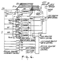
- FIG. 4 is a detailed block diagram of the lock logic of the present invention.
- Figure 4a is a block diagram of a lock register entry.
- Figure 4b is a diagram of an entry in the lock queue.
- Figure 5 is a diagram of the lock queue at the processor level in the system of Figure 1.
- Fig. 1 is a block diagram of a system which advantageously uses the present invention. As illustrated, there are four CPU's O-3 indicated as blocks 11-14, respectively. These blocks 11-14 are coupled to a central unit, indicated by dashed line 15, to be described in more detail below. Each of the CPUs 11-14 is connected to the central unit 15 over a point to point bus, hereinafter referred to as an E-BUS TA, the E-BUS TA for CPU 0 being designated as 17, the corresponding bus for CPU 1 as 18, and so on accordingly. Each CPU 11-14 also receives output on an E-BUS FA from the central unit 15, the four buses being designated respectively as 21 through 24.
- E-BUS TA point to point bus
- each of the CPUs 11-14 communicates with a bus adaptor XJA 25 over two 16-bit buses, i.e., an input and an output bus, with the bus adaptor 25 converting this information to another bus 27.
- a console 26 is associated with at least one of the CPUs 11-14.
- the system also includes a shared memory made up of a plurality of memory modules 31a to 31n which are coupled to the central unit 15 over what is designated A-BUS FA 33 and what is designated as A-BUS TA 35.
- the A-BUS FA 33 carries outputs from the central unit 15 to the memory modules and the bus 35 provides memory information to the central unit 15.
- buses 17-24 and 33 are 32-bit parallel buses and bus 35 is a 64-bit parallel bus.
- the E-BUSES operate at 8ns timing and the A-BUSES at 16ns in this embodiment.
- Fig. 1 further shows a configuration for the central unit 15.
- a multiplexer, designated generally by 37, is provided in the central unit 15.
- the multiplexer 37 is made up of several multiplexers advantageously coupled together.
- a port logic block 49 composed of port logic units 49a.
- Each port logic unit 49a includes a buffer 53 for each input port, i.e., each E-BUS TA 17-20.
- Each of the buffers 53 in the port logic units 49a can hold three words for each of buses 17-20 from CPUs 11-14.
- Outputs from the buffers 53 are coupled into scheduler arbitrator logic 50 which arbitration logic 50 provides outputs to control multiplexer 37.
- One of the general outputs of MUX 37 is fed to a write buffer 10 which is coupled to memory modules 31a-n via the bus 33.
- Fig. 2 is a more detailed block diagram of the central unit 15 of Fig. 1 showing a port select logic 65 and resource check 67 which together compose the scheduler/arbitrator 50 of Fig. 1 and its relationship to other elements of the system.
- Port select logic 65 is combined with multiplexer 37a to form scheduling logic 66.
- Resource check logic 67 combines with MUX 37b and state device 42 to form arbitrator 51.
- the buses 17-20 are inputs to the port logic 49.
- Each CPU is considered a system port.
- Individual port logic units, designated 49a-d, are provided for each of the buses 17-20.
- the bus information enters a state device 53a, forming part of the buffer 53 of Fig.
- the buffer 53b has storage space for three words.
- the output from the state device 53a is also provided into validity logic 57.
- the validity logic 57 controls a port multiplexer 59.
- the validity logic 57 also receives a port grant signal on line 61 from the arbitrator 51.
- Validity logic 57 determines whether or not a command or data are valid and which of the data, either in the buffers 53b or on the input line from the state device 53a, is to be switched out onto an output line 63 which provides one of the inputs to a multiplexer 37a (part of MUX 37 in Fig. 1).
- the outputs on lines 63 from the port multiplexers 59 are the inputs to the multiplexer 37a.
- port selection or scheduling logic 65 Associated with the multiplexer 37a is port selection or scheduling logic 65.
- the port select logic 65 selects one of the four input lines 63 to be coupled to the output of multiplexer 37a. This, of course, must be coordinated with the operation of the logic 57 which is switching outputs onto the lines 63.
- the port select logic 65 basically operates so as to provide the four ports providing their inputs on line 63 a round robin access to bus 36.
- Bus 36 is an input to a resource check block 67 which is part of the arbitrator 51.
- Bus 36 is also an input to the multiplexer 37b (also part of MUX 37 in Fig. 1).
- Bus 36 is also coupled to a memory map unit (“MMAP") 69, lock logic unit (“LOCK”) 71, input/output unit (“CPIO”) 73, interrupt request unit (“IREQ/SNIT”) 75, memory controller (“MEMC/DBEC”) 77 and memory write data path unit (“MWDP”) 79.
- MMAP memory map unit
- LOCK lock logic unit
- CPIO input/output unit
- IREQ/SNIT interrupt request unit
- MEMC/DBEC memory controller
- MWDP memory write data path unit
- Each of the blocks 69, 71, 73, 75 and 77 also provide inputs to the multiplexer 37b.
- the resource check 67 can provide an ARB command to the multiplexer 37b.
- the previously described A-BUS TA is provided as an input to a memory read data path 81 which provides its input into the memory controller, i.e., the MEMC/DEBC 77, the output of which is the memory controller refill data which is one of the inputs to multiplexer 37b.
- An output of MEMC/DBEC 77 is also provided onto the line 33, i.e., the A-BUS FA line.
- the output from the multiplexer 37b is provided through a state device 42.
- the output of state device 42 forms the E-BUS FA buses that couple to all the CPUs.
- Each of the blocks 69, 71, 73, 75, 77 and 79 provide an input to the resource check 67 which utilizes this information and the presence of a command on the bus 36 to arbitrate between the different inputs which want access to the multiplexer 37b. It grants access via its output lines coupled through state devices 67a and 67b.
- One set of output lines is the output lines 83 leading from the resource check 67 to each of the blocks 69, 71, 73, 75, 77 and 79.
- the other are the lines 61 and 85 leading, respectively, to the port logic 49 and the port select logic 65.
- Fig. 3 is a more detailed block diagram of one of the CPU modules 11-14 (in this case CPU 0) shown in Fig. 1.
- the CPU module 11 has three major component chips including an interface (X) chip 102, a processor (P) chip 104 and cache interface (CF) chip 100.
- the processing chip or P chip 104 is coupled with a cache memory 106.
- the processing chip 104 further couples with a cache tag store 110 by which it requests an address over line 112 and receives a tag entry via line 114.
- the P chip 104 makes use of lines 116 to enable data to be written to the cache memory 106. Further, lines 118 provide the data and error correction codes (ECC) from the cache memory 106 to the processing chip 104.
- ECC error correction codes
- the cache memory 106 is shown in this example composed of random access memories (RAMs).
- the cache 106 further receives data and ECC information from the CF chip 100 over lines 120.
- the operation of a cache memory 106 along with its associated cache tag store 110 is well known to those skilled in the art and will not therefore be discussed.
- the X chip 102 provides an interface to the XJA bus adaptor 25 (Fig. 1).
- the X chip 102 provides outputs to the CF chip 100 and receives inputs therefrom. Further, the X chip 102 interfaces with a console support block 108 for interfacing with a console terminal 26 (Fig. 1).
- the CF chip 100 provides outputs to the cache tag store 110 including new tag entry and write enable information. Further, the CF chip 100 receives address and data operands, along with parity information, from the processing chip 104. The CF chip 100 couples the CPU with the E BUS TA and E BUS FA as indicated by bus lines 17 and 21, respectively.
- a device such as one of the CPU modules O-3 or an I/O unit or device through the XJA adaptor to gain exclusive access to a particular unit or location of the memories 31a-31n.
- one of the CPU modules 11-14 may desire to lock a block of data, a longword, a byte, etc., in one of the memory modules 31a-31n.
- the device generates a lock request in the form of a READ LOCK command. This command will lock the particular memory location allowing the resource exclusive access thereto. Once the location is locked no other CPU's lock request to that location will be allowed.
- a WRITE UNLOCK command is generated to free the memory location. The precise operation of these commands is described below with respect to Figure 4.
- each node on the E BUS in this case the CPUs, also includes more than one resource which may generate lock requests, for example, the P chip 104 or the X chip 102.
- the CF chip 100 functions to insure that neither the processing chip's 104 or X chip's 102 lock requests are locked out from being serviced.
- the central unit 15 must insure that no lock out occurs for any of the nodes on the E BUS.
- the central unit 15 makes use of lock block 71 which includes lock logic to be described below in Fig. 4, to insure that no node is ever locked out from having its lock request satisfied.
- the CF chip 100 in the CPU shown in Fig. 3 includes lock logic 125 for insuring that neither the CPU nor the X chip are ever locked out from having their lock requests satisfied.
- a hierarchy of lock out avoidance mechanisms i.e., lock logic 71 and lock logic 125, are utilized to insure that every lock request is eventually serviced.
- lockout avoidance is performed at the highest level by the lock logic 71 in the central unit 15.
- the use of the central unit 15 to keep track of lock locations and to avoid lockouts provides an advantage over conventional multi-drop buses wherein each CPU or memory coupled to the bus must keep track of the locked data. Because the central unit 15 receives all lock requests and maintains lock registers, it provides the opportunity to implement centralized queueing mechanisms to avoid the lockouts.
- the lock logic 71 includes a predetermined number of lock registers 80a-80n, in the example shown "n" equals eight, but it is understood to depend upon the requirements of the system.
- Each of the lock registers 80a-80n stores the address of a particular memory location to be locked. For this example having eight lock registers, up to eight memory locations can be locked at any given time.
- the outputs from each of the register blocks 80a-80n are the result of a compare performed between each of the lock registers and the address of an incoming lock request on bus 36.
- the output of OR gate 82 provides either a LOCK HIT or LOCK MISS signal.
- the LOCK HIT signal is provided to further logic 84 which outputs a LOCK REFUSED signal to the resource check 67 in the arbiter 51 (Fig. 2).
- the LOCK MISS signal is provided as an input to a write control 86.
- Each lock register 80a-80n includes a register 88 and a comparator 90.
- the register 88 stores an address of the memory location desired to be locked along with an indication of its validity, i.e., locked or unlocked, as shown in Fig. 4a.
- the register 88 is composed of several fields including a lock register valid bit field, node source ID, and byte addresses.
- the register 88 is enabled via commands from the write control block 86.
- the command and address received from the schedule logic 66 (Fig. 2) over bus 36 is provided in parallel to the comparators 90 in each of the lock registers 80a-80n.
- the command and address are further provided to delay logic 92 which has an output coupled in parallel to the registers 88 in each of the lock registers 80a-80n.
- the output from the registers 88 are provided as another input to the comparators 90 in each of the lock registers.
- the output from the comparators 90 in each of the lock registers is then provided to the OR gate 82 mentioned above.
- a lock queue shown generally by dotted line 130, is composed of several state devices 94a-94d chained together.
- the number of entries in the lock queue correspond to the number of nodes.
- An example of one of the state devices 94a-94d is shown in greater detail in Fig. 4b functioning as a lock queue register entry including a lock queue register valid bit and node source ID bits. Coupled with each state device 94a-94d is an associated multiplexer 96a-96d.
- the registers 94a-94d and multiplexers 96a-96d are coupled together to form the lock queue 130 which functions as will be described below.
- a comparator 98a-98d is associated with each individual state device and multiplexer 94, 96 and receives an input therefrom. Further, the comparator 98 receives an input from the command address bus 36. Each of the comparators 98a-98d provides an output to OR gate 99.
- the OR gate 99 provides inputs to OR gate 84 and to write control logic 86.
- the write control logic 86 also receives inputs from each comparator 90 in the lock register blocks 80a-80n and each comparator 98a-98d associated with the lock queue 130.
- the write control logic 86 provides a LOCK REGISTER WRITE CONTROL signal to each of the registers 88 in the lock registers 80a-80n. Further, the write control block 86 provides a LOCK QUEUE REGISTER WRITE CONTROL signal to enable the multiplexers 96a-96d associated with state devices 94a-94d to operate in accordance with the lock queue 130 design. Also, a REFUSAL COUNTER INCREMENT CONTROL signal is provided from write control 86 to a plurality of refusal counters 131-136. Each refusal counter is associated with a node, such as CPU modules 0-3 (Fig. 1) in the system. The refusal counters 131-136 are incremented by signals from the write control 86.
- an END OF COUNT signal is provided to the write control 86.
- the predetermined limit in the refusal counter is optimized for the best performance for lock requests in the system.
- the write control 86 further receives from the arbiter 51 (Fig. 2) a LOCK CLEAR and LOCK SET signal.
- a READ LOCK command and an associated memory address to be locked are provided in parallel to the comparators 90 in each of the lock registers 80a-80n.
- Each of the respective comparators 90 compares the address with the address previously stored in its associated register 88.
- the comparators 90 do not generate any matches as an output to the OR gate 82. Therefore, the output from the OR gate 82 provides a LOCK MISS signal to the write control 86.
- the write control 86 then provides a LOCK REGISTER WRITE CONTROL signal to registers 88 to enable a particular one of the registers 88 in the lock registers 80a-80n and to set the valid bit.
- the particular block which is enabled by the LOCK REGISTER WRITE CONTROL signal is determined by a predefined protocol in the write control 86.
- the READ LOCK command stores its associated address in the register 88 from line 89 after having been provided as an input thereto from bus 36 through the delay logic 92. Further the write control 86 sets the valid bit in register 88 to indicate the memory location is locked.
- the delay logic 92 functions to sufficiently delay the command and address so as to arrive at the register 88 once the write control 86 generates its LOCK REGISTER WRITE CONTROL signal, enabling storage at a predetermined location. In this manner, up to eight lock addresses can be stored in the lock registers 80a-80n.
- WRITE UNLOCK command Associated with each READ LOCK command is a WRITE UNLOCK command and associated address.
- the WRITE UNLOCK command is necessary to unlock the particular memory location once the resource has finished its use. Referring back to Fig. 4, WRITEUNLOCK commands are never refused by the lock logic 71.
- a WRITE UNLOCK command and associated address on bus 36 provides a LOCK MISS output to the write control 86 which provides a LOCK REGISTER WRITE CONTROL signal to clear the valid bit in the particular register 88 in the lock register block 80a-80n corresponding to the WRITE UNLOCK command.
- the LOCK REFUSED signal is provided as an input to the resource check 67 which enables multiplexer 37b to provide a retry signal on the particular E BUS 21-24 from which the READ LOCK command was generated.
- a signal is sent over line 200 to the write control 86.
- the match indicates that the memory location is currently locked.
- the write control 86 then provides a REFUSAL COUNTER INCREMENT CONTROL signal.
- the REFUSAL COUNTER INCREMENT CONTROL signal enables the particular refusal counter 130-136 associated with the node generating the READ LOCK command which was refused. This signal increments the counter.
- the END OF COUNT signal is provided to the write control 86.
- This generates a LOCK QUEUE REGISTER WRITE CONTROL signal from the write control 86 to the lock queue 130.
- the node source ID and the lock queue register valid bit (Fig. 4b) are then loaded and set, respectively, into the top of the queue 94d by enabling the multiplexer 96d for the particular READ LOCK command and associated address from bus 36.
- This lock request then becomes the head of the lock queue 130.
- the lock queue 130 contains a valid entry, any subsequent lock requests from other nodes will be automatically refused (regardless of whether the other conditions for refusing locks are satisfied) and will be stored in the queue 130.
- the LOCK QUEUE REGISTER WRITE CONTROL signal can implement several functions. These functions include a Hold signal, Update signal and Push To Top of Queue signal. These signals are described below with respect to the queue 130 operation.
- the LOCK QUEUE REGISTER WRITE CONTROL signal is next input to multiplexer 96c which enables the second lock request to be stored in location 96c in the lock queue 130. If another lock request is generated from a node already stored in the lock queue 130, that request will then generate the LOCK QUEUE REGISTER WRITE CONTROL hold signal that enables the middle line of the multiplexers currently storing the same entry 94. This new request then is stored in the same queue position.
- Each entry in the lock queue 130 is provided as an input to its associated comparator 98a-98d. Further, the information on bus 36 is also provided to each of the comparators 98a-98d. The output from the comparators 98a-98d are provided as parallel inputs to OR gate 99 which provides an output both to OR gate 84 (QUEUE HIT) and to write control 86.
- the lock queue 130 has as many entries as there are nodes coupled to the central unit 15.
- the four entry lock queue i.e., entries 94a-94d
- each entry in the queue 130 is composed of two parts: a valid bit, indicating whether the entry is valid, and a slot ID which points to one of the E BUS CPU nodes.
- the lock queue 130 Every time the head entry 94d of the lock queue 130 is serviced, i.e., its lock request is satisfied, the lock queue is pushed by the LOCK QUEUE REGISTER WRITE CONTROL push to top of queue signal enabling the lower input to the multiplexers 96a-96d. This has the effect of pushing the entries upward in the queue to create a new head of queue and making available the bottom entry 94a. For this reason, the lock queue 130 need only be of a depth equal to the number of nodes on the E BUS which can generate lock requests.
- Lock requests are generated from the various nodes (Fig. 1) in the form of READ LOCK commands and an associated address location and are received by the central unit 15 through their respective port logics 49a.
- the request passes through the scheduling logic 66 and into the lock logic 71 (Fig. 2) on bus 36.
- the lock request does not enter the lock queue 130 (Fig. 4).
- the write control 86 increments the refusal counter 131-136 for the particular node, in this case CPU 0.
- CPU 0 After a predetermined period of time, CPU 0 again retries its lock request. If the lock request from CPU 0 is again refused, its respective refusal counter is incremented once more. Once a lock request has been refused a predetermined consecutive number of times while the lock queue 130 remains empty, the write control 86 then places the identification for the particular node at the head of the lock queue 130. Only the node ID (Fig. 4b) is stored in the lock queue and not the address of the lock request that was refused.
- lock queue 130 is no longer empty, a subsequently arbitrated lock request from any other node will be refused and will also enter the lock queue 130 in the order in which it is serviced by the arbiter 51.
- the next waiting lock request in the lock queue 130 is pushed to the head of the queue via the LOCK QUEUE REGISTER WRITE CONTROL push to top of queue signal and the operation of the multiplexers 96a-96d.
- This operation assures that whenever the lock queue 130 is empty, it is difficult to enter the lock queue 130 because the lock requests from a particular node must be refused a predetermined consecutive number of times. Therefore, the lock queue 130 is predominantly kept empty, assuming the refusal counter is set at a high enough value. However, once the lock queue 130 has an entry, all future lock requests are serviced strictly by their lock queue position, i.e., the head of the queue gets satisfied first, the second entry is satisfied next, etc. This operation continues until the lock queue 130 is again empty.
- the lock logic generates a LOCK REFUSED signaling response to a READ LOCK command from a node in three instances: 1) the lock queue is not empty and the requesting node is not the head of the queue; 2) no free lock registers are available; or 3) the particular memory block desired is already locked.
- the central unit 15 guarantees that every lock request, regardless of its address, has a fair and equal chance of entering the lock queue 130 and hence, eventually reaching the head of the lock queue 130 for servicing.
- the CPU block diagram includes the CF chip 100 which has a lock logic 125.
- This lock logic 125 prevents lockouts of either the processor chip's 104 or X chip's 102 lock requests.
- the lock logic 125 operates similarly to the lock logic 71 shown in Fig. 2. Because the lock queue 130 in the central unit 15 does not store addresses nor whether the lock request was from either the X chip or the processor chip 104, it is possible that either the processor chip or the X chip can lock the other out from ever having their lock request satisfied.
- Fig. 5 illustrates the two entry queue used in the lock logic 125 of the CF chip 100.
- the queue 134 includes two entries, each of which includes two bits: 1) an entry valid bit; and 2) a source ID bit, e.g., X chip or processor chip.
- the queue 134 remains empty. However, once a lock request from, for example, the processor chip, is refused by the central unit 15, the lock request immediately enters the head of the queue 134. From this point onward, only the processor chip can have its lock requests forwarded onto the E BUS (and hence to the central unit 15) from the CF chip 100. If, for example, the X chip requests a lock, this request will enter the queue 134 behind the processor chip's entry. Further, the X chip's lock requests will internally be refused by the CF chip 100 and thus prevented from going onto the E BUS.
- the processor chip entry is eventually satisfied by the central unit 15, it is popped out of the queue 134 and the X chip's lock request becomes the new head of the queue 134.
- the method used in the CF chip 100 for avoiding lockouts is as follows. If the queue 134 is empty, both the processor and X chip can send their respective lock requests to the central unit 15 via the E BUS 17-20. If a lock request is refused by the central unit 15, then the source of the lock request, i.e., processor or X chip, along with whether it is valid or invalid, is entered into the queue 134. It is important to note that if the source is already stored in the queue, it will maintain its queue position.
- the protocol used in the CF chip to avoid lockouts is essentially similar to the lock queue 130 used in the central unit. However, in this instance there is no need to implement a refusal counter in the CF chip 100, because the frequency at which lock requests are generated from the X chip at the CPU level is not great enough to require the use of a refusal counter.
Abstract
Description
- This invention relates to a computer system and, more particularly, to a lock out avoidance mechanism used in the computer system to prevent a situation wherein lock requests generated by the system devices are never serviced by the system.
- In multiprocessor systems, any of a number of processors or devices may desire exclusive access to a shared resource in the system. These shared resources can be, for example, a memory location such as a block of memory, longword, byte, etc. In order to obtain exclusive rights to the memory location, the processor generates an interlock signal in the form of a lock request which will lock that particular location in memory to a device requesting access and thus deny any other processor or device interlocked access to the particular memory location. Once the processor finishes with the particular memory location, an unlock request is generated to unlock the location, thus again allowing general access.
- The use of lock requests occurs most often when processors share a resource such as a particular data structure or table stored in the memory. In order to gain access to such shared resource, the processors synchronize using interlocked operation in memory locations sometimes referred to as semaphores. Becuase only one processor is granted exclusive access to the semaphore any operations on the shared resource is thus serialized. It is possible that multiple processors wishing to access the resource simultaneously may generate lock requests for the semaphore. For example, if a system includes four processors (CPUs) or nodes from which lock requests can originate, it is possible for two or more processors to desire interlocked access to the same location at the same time. In this instance, one of the requests is refused and the refused node receives a retry signal instructing it to retry the lock request. Typically, each of the CPUs or the memory itself must keep track of the locked memory locations, status of any pending lock requests, etc. In other systems using a central arbiter to receive the lock requests, the tracking of the lock requests occurs at the central arbiter. In either system it is possible, when multiple nodes require locked access to the same memory location, for one or more nodes to be denied access forever. This condition is referred to as lockout.
- Further, many systems include several levels of processing, with each level having multiple sources which can generate lock requests. Therefore, lock out may occur at any level in the system wherein multiple lock requests are generated. In previous system designs the lock out condition was resolved either by throttling all requestors except the node locked out when this condition was detected by the system or by forcing queuing of all locked requests which enforced sequentiality. This resulted in either a complex lockout avoidance protocol or slowed the system performance with respect to lock requests.
- The present invention overcomes these problems by providing an efficient and simple hierarchical system of lock out avoidance mechanisms for use in systems having central locations for receiving the lock requests. To avoid lock out each of the mechanisms uses a centralized queueing structure called a lock queue. The centralized queueing mechanism is used because all interlock signals, e.g. lock requests and unlock requests, are received at the central location. The lock queue contains as many entries as there are possible nodes from which lock requests can originate, but no one entry is specifically tied to any node. Each entry in the lock queue contains a valid indication field and a node identification (I.D.) field. The valid indication field indicates whether the lock request is valid and the node I.D. field stores the identification of the node generating the lock request. The lock queue further has a head and a tail entry. The head points to the first entry, i.e., the highest priority entry, in the queue and the tail points to the first available entry in the lock queue. Each time the head of the queue is serviced, i.e., its lock request is satisfied, the head of the queue moves to the next entry in line. If one of the nodes already has an entry in the queue which has not yet been serviced, then subsequent lock requests from that node will be written into the same place in the lock queue. This is possible because the entries only contain the node ID and not the request itself. In this manner, the lock queue need only contain a number of entries corresponding to the number of nodes from which lock requests can originate.
- The lock queue is usually empty and lock requests, from the various nodes passing through the central location, only enter the lock queue, if, after a predetermined number of tries, they are unable to gain access to a particular resource. For example, assume that a lock request from
node 0 is refused access because the particular memory location was already locked or a register for allowing the lock request was not available, then the central location increments a refusal counter for the particular node. When the node, in thiscase node 0, retries its lock request, it will then again be either refused or granted access. If the lock request is refused a predetermined consecutive number of times while the lock queue is empty, then the node's I.D. will be stored at the head of the lock queue along with an indication of its validity. - Because the lock queue is no longer empty, any subsequent lock requests from any other node in the system will be refused access to any location and will immediately enter the lock queue in the order in which they are serviced by the central location. When a lock request at the head of the queue is serviced, then the next waiting request in the queue becomes the head of the queue.
- In this manner, a lock out avoidance mechanism is operated such that if the lock queue is empty, it is difficult to enter the lock queue because a particular lock request must be refused the predetermined number of times before the lock request may enter the queue. Once in the queue, the lock requests are serviced serially which slows down the system. Therefore, the lock queue is operated to try to keep the queue empty by using the refusal counter. This operation ensures that the queue is usually empty. However, once the lock queue is no longer empty, all future lock requests are serviced strictly by their queue position. This operation continues until the lock queue again becomes empty. Thus, the lock out avoidance mechanism at this level guarantees that each node will eventually have its lock request serviced.
- The present invention provides a similar lock out avoidance scheme at each level in the system wherein a lock out condition can occur. For example, a typical multiprocessor system has a number of hierarchical levels. A first level has each of the processors in the system vying for access to the system bus. The second level has devices within each processor, such as a processor chip and an interface chip, vying for access to the processor's bus. Further levels can include devices coupling through the interface chip which try to access the interface bus, etc.
- Assuming in our second level that for each processor of a multiprocessor system, there are two sources of lock requests, i.e., the processor chip itself and other devices interfacing therewith, then the lock out avoidance mechanism at this level consists of a two entry queue. Each entry in the queue contains two fields: 1) an entry valid and 2) source I.D. As long as the lock requests are not refused, the queue will remain empty. However, if a lock request from, for example, the processor chip is refused, then that lock request immediately enters the head of the queue. From that point onward until the request is granted, only the processor chip's lock requests can be output onto a bus to the central location. If another device generates a lock request at the second level, the lock request enters the queue behind the processor chip's entry and is internally refused by the processor. When the head of the queue's lock request is eventually satisfied, i.e., the processor chip is finally granted access, the entry is popped from the queue and the next device becomes the head of the queue. Thus, a lock out avoidance mechanism is provided at a second level in the system.
- As a result of providing a lock out avoidance mechanism at each level wherein multiple sources can generate lock requests and hence lock outs could occur, the present invention guarantees that every lock request generated in the system will eventually be serviced.
- Figure 1 is a block diagram of a system advantageously employing the present invention.
- Figure 2 is a block diagram of the central arbiter including the lock logic of the present invention.
- Figure 3 is a block diagram of one of the CPU modules in Figure 1.
- Figure 4 is a detailed block diagram of the lock logic of the present invention.
- Figure 4a is a block diagram of a lock register entry.
- Figure 4b is a diagram of an entry in the lock queue.
- Figure 5 is a diagram of the lock queue at the processor level in the system of Figure 1.
- Fig. 1 is a block diagram of a system which advantageously uses the present invention. As illustrated, there are four CPU's O-3 indicated as blocks 11-14, respectively. These blocks 11-14 are coupled to a central unit, indicated by dashed line 15, to be described in more detail below. Each of the CPUs 11-14 is connected to the central unit 15 over a point to point bus, hereinafter referred to as an E-BUS TA, the E-BUS TA for
CPU 0 being designated as 17, the corresponding bus forCPU 1 as 18, and so on accordingly. Each CPU 11-14 also receives output on an E-BUS FA from the central unit 15, the four buses being designated respectively as 21 through 24. Also shown in the illustrated embodiment, each of the CPUs 11-14 communicates with abus adaptor XJA 25 over two 16-bit buses, i.e., an input and an output bus, with thebus adaptor 25 converting this information to anotherbus 27. Aconsole 26 is associated with at least one of the CPUs 11-14. - The system also includes a shared memory made up of a plurality of memory modules 31a to 31n which are coupled to the central unit 15 over what is designated
A-BUS FA 33 and what is designated asA-BUS TA 35. TheA-BUS FA 33 carries outputs from the central unit 15 to the memory modules and thebus 35 provides memory information to the central unit 15. In the illustrated embodiment, buses 17-24 and 33 are 32-bit parallel buses andbus 35 is a 64-bit parallel bus. The E-BUSES operate at 8ns timing and the A-BUSES at 16ns in this embodiment. - Fig. 1 further shows a configuration for the central unit 15. A multiplexer, designated generally by 37, is provided in the central unit 15. As will be shown below, the
multiplexer 37 is made up of several multiplexers advantageously coupled together. At the inputs to themultiplexer 37 is aport logic block 49 composed ofport logic units 49a. Eachport logic unit 49a includes a buffer 53 for each input port, i.e., each E-BUS TA 17-20. Each of the buffers 53 in theport logic units 49a can hold three words for each of buses 17-20 from CPUs 11-14. Outputs from the buffers 53 are coupled into scheduler arbitrator logic 50 which arbitration logic 50 provides outputs to controlmultiplexer 37. One of the general outputs ofMUX 37 is fed to awrite buffer 10 which is coupled to memory modules 31a-n via thebus 33. - Fig. 2 is a more detailed block diagram of the central unit 15 of Fig. 1 showing a port
select logic 65 andresource check 67 which together compose the scheduler/arbitrator 50 of Fig. 1 and its relationship to other elements of the system. Portselect logic 65 is combined with multiplexer 37a to formscheduling logic 66.Resource check logic 67 combines withMUX 37b andstate device 42 to formarbitrator 51. As illustrated, the buses 17-20 are inputs to theport logic 49. Each CPU is considered a system port. Individual port logic units, designated 49a-d, are provided for each of the buses 17-20. The bus information enters a state device 53a, forming part of the buffer 53 of Fig. 1, from which it is directed to buffer 53b, also forming part of buffer 53 in Fig. 1. The buffer 53b has storage space for three words. The output from the state device 53a is also provided intovalidity logic 57. Thevalidity logic 57 controls a port multiplexer 59. Thevalidity logic 57 also receives a port grant signal online 61 from thearbitrator 51.Validity logic 57 determines whether or not a command or data are valid and which of the data, either in the buffers 53b or on the input line from the state device 53a, is to be switched out onto anoutput line 63 which provides one of the inputs to a multiplexer 37a (part ofMUX 37 in Fig. 1). The outputs onlines 63 from the port multiplexers 59 are the inputs to the multiplexer 37a. Associated with the multiplexer 37a is port selection orscheduling logic 65. In response to outputs from thearbitrator 51, and its own logic, the portselect logic 65 selects one of the fourinput lines 63 to be coupled to the output of multiplexer 37a. This, of course, must be coordinated with the operation of thelogic 57 which is switching outputs onto thelines 63. The portselect logic 65 basically operates so as to provide the four ports providing their inputs on line 63 a round robin access tobus 36. -
Bus 36 is an input to aresource check block 67 which is part of thearbitrator 51.Bus 36 is also an input to themultiplexer 37b (also part ofMUX 37 in Fig. 1).Bus 36 is also coupled to a memory map unit ("MMAP") 69, lock logic unit ("LOCK") 71, input/output unit ("CPIO") 73, interrupt request unit ("IREQ/SNIT") 75, memory controller ("MEMC/DBEC") 77 and memory write data path unit ("MWDP") 79. Each of theblocks multiplexer 37b. In addition, theresource check 67 can provide an ARB command to themultiplexer 37b. - The previously described A-BUS TA is provided as an input to a memory read data path 81 which provides its input into the memory controller, i.e., the MEMC/
DEBC 77, the output of which is the memory controller refill data which is one of the inputs tomultiplexer 37b. An output of MEMC/DBEC 77 is also provided onto theline 33, i.e., the A-BUS FA line. The output from themultiplexer 37b is provided through astate device 42. The output ofstate device 42 forms the E-BUS FA buses that couple to all the CPUs. - Each of the
blocks resource check 67 which utilizes this information and the presence of a command on thebus 36 to arbitrate between the different inputs which want access to themultiplexer 37b. It grants access via its output lines coupled throughstate devices 67a and 67b. One set of output lines is theoutput lines 83 leading from theresource check 67 to each of theblocks lines 61 and 85 leading, respectively, to theport logic 49 and the portselect logic 65. - Fig. 3 is a more detailed block diagram of one of the CPU modules 11-14 (in this case CPU 0) shown in Fig. 1. The
CPU module 11 has three major component chips including an interface (X)chip 102, a processor (P)chip 104 and cache interface (CF)chip 100. The processing chip orP chip 104 is coupled with acache memory 106. Theprocessing chip 104 further couples with acache tag store 110 by which it requests an address overline 112 and receives a tag entry vialine 114. TheP chip 104 makes use oflines 116 to enable data to be written to thecache memory 106. Further,lines 118 provide the data and error correction codes (ECC) from thecache memory 106 to theprocessing chip 104. - The
cache memory 106 is shown in this example composed of random access memories (RAMs). Thecache 106 further receives data and ECC information from theCF chip 100 over lines 120. The operation of acache memory 106 along with its associatedcache tag store 110 is well known to those skilled in the art and will not therefore be discussed. - The
X chip 102 provides an interface to the XJA bus adaptor 25 (Fig. 1). TheX chip 102 provides outputs to theCF chip 100 and receives inputs therefrom. Further, theX chip 102 interfaces with a console support block 108 for interfacing with a console terminal 26 (Fig. 1). - The
CF chip 100 provides outputs to thecache tag store 110 including new tag entry and write enable information. Further, theCF chip 100 receives address and data operands, along with parity information, from theprocessing chip 104. TheCF chip 100 couples the CPU with the E BUS TA and E BUS FA as indicated bybus lines - Referring back to Fig. 1, it is often desirable for some device such as one of the CPU modules O-3 or an I/O unit or device through the XJA adaptor to gain exclusive access to a particular unit or location of the memories 31a-31n. For example, one of the CPU modules 11-14 may desire to lock a block of data, a longword, a byte, etc., in one of the memory modules 31a-31n. To do so, the device generates a lock request in the form of a READ LOCK command. This command will lock the particular memory location allowing the resource exclusive access thereto. Once the location is locked no other CPU's lock request to that location will be allowed. Once the resource has completed its operations on the location, a WRITE UNLOCK command is generated to free the memory location. The precise operation of these commands is described below with respect to Figure 4.
- In the example of Fig. 1, there are four E BUS nodes, corresponding to CPU modules 0-3, from which lock requests can originate. Still further, as seen from Fig. 3, each node on the E BUS, in this case the CPUs, also includes more than one resource which may generate lock requests, for example, the
P chip 104 or theX chip 102. In this instance, theCF chip 100 functions to insure that neither the processing chip's 104 or X chip's 102 lock requests are locked out from being serviced. Similarly, the central unit 15 must insure that no lock out occurs for any of the nodes on the E BUS. - Referring to Fig. 2, the central unit 15 makes use of
lock block 71 which includes lock logic to be described below in Fig. 4, to insure that no node is ever locked out from having its lock request satisfied. Further, theCF chip 100 in the CPU shown in Fig. 3 includes lock logic 125 for insuring that neither the CPU nor the X chip are ever locked out from having their lock requests satisfied. In this manner as will be fully described below, a hierarchy of lock out avoidance mechanisms, i.e., locklogic 71 and lock logic 125, are utilized to insure that every lock request is eventually serviced. - Referring to Fig. 2, lockout avoidance is performed at the highest level by the
lock logic 71 in the central unit 15. The use of the central unit 15 to keep track of lock locations and to avoid lockouts provides an advantage over conventional multi-drop buses wherein each CPU or memory coupled to the bus must keep track of the locked data. Because the central unit 15 receives all lock requests and maintains lock registers, it provides the opportunity to implement centralized queueing mechanisms to avoid the lockouts. - Fig. 4 describes in greater detail the
lock logic 71. Thelock logic 71 includes a predetermined number of lock registers 80a-80n, in the example shown "n" equals eight, but it is understood to depend upon the requirements of the system. Each of the lock registers 80a-80n stores the address of a particular memory location to be locked. For this example having eight lock registers, up to eight memory locations can be locked at any given time. The outputs from each of the register blocks 80a-80n are the result of a compare performed between each of the lock registers and the address of an incoming lock request onbus 36. The output ofOR gate 82 provides either a LOCK HIT or LOCK MISS signal. The LOCK HIT signal is provided tofurther logic 84 which outputs a LOCK REFUSED signal to theresource check 67 in the arbiter 51 (Fig. 2). The LOCK MISS signal is provided as an input to awrite control 86. - Each lock register 80a-80n includes a
register 88 and acomparator 90. Theregister 88 stores an address of the memory location desired to be locked along with an indication of its validity, i.e., locked or unlocked, as shown in Fig. 4a. Theregister 88 is composed of several fields including a lock register valid bit field, node source ID, and byte addresses. Theregister 88 is enabled via commands from thewrite control block 86. - The command and address received from the schedule logic 66 (Fig. 2) over
bus 36 is provided in parallel to thecomparators 90 in each of the lock registers 80a-80n. The command and address are further provided to delaylogic 92 which has an output coupled in parallel to theregisters 88 in each of the lock registers 80a-80n. The output from theregisters 88 are provided as another input to thecomparators 90 in each of the lock registers. The output from thecomparators 90 in each of the lock registers is then provided to theOR gate 82 mentioned above. - A lock queue, shown generally by dotted
line 130, is composed of several state devices 94a-94d chained together. The number of entries in the lock queue (in this example four) correspond to the number of nodes. An example of one of the state devices 94a-94d is shown in greater detail in Fig. 4b functioning as a lock queue register entry including a lock queue register valid bit and node source ID bits. Coupled with each state device 94a-94d is an associated multiplexer 96a-96d. The registers 94a-94d and multiplexers 96a-96d are coupled together to form thelock queue 130 which functions as will be described below. A comparator 98a-98d is associated with each individual state device andmultiplexer 94, 96 and receives an input therefrom. Further, the comparator 98 receives an input from thecommand address bus 36. Each of the comparators 98a-98d provides an output to OR gate 99. The OR gate 99 provides inputs to ORgate 84 and to writecontrol logic 86. Thewrite control logic 86 also receives inputs from eachcomparator 90 in the lock register blocks 80a-80n and each comparator 98a-98d associated with thelock queue 130. - The
write control logic 86 provides a LOCK REGISTER WRITE CONTROL signal to each of theregisters 88 in the lock registers 80a-80n. Further, thewrite control block 86 provides a LOCK QUEUE REGISTER WRITE CONTROL signal to enable the multiplexers 96a-96d associated with state devices 94a-94d to operate in accordance with thelock queue 130 design. Also, a REFUSAL COUNTER INCREMENT CONTROL signal is provided fromwrite control 86 to a plurality of refusal counters 131-136. Each refusal counter is associated with a node, such as CPU modules 0-3 (Fig. 1) in the system. The refusal counters 131-136 are incremented by signals from thewrite control 86. Once a particular refusal counter reaches a predetermined limit, an END OF COUNT signal is provided to thewrite control 86. The predetermined limit in the refusal counter is optimized for the best performance for lock requests in the system. Thewrite control 86 further receives from the arbiter 51 (Fig. 2) a LOCK CLEAR and LOCK SET signal. - In operation, assuming all of the lock registers 80a-80n are available for use, a READ LOCK command and an associated memory address to be locked are provided in parallel to the
comparators 90 in each of the lock registers 80a-80n. Each of therespective comparators 90 compares the address with the address previously stored in its associatedregister 88. In this example, because each of the lock registers is initially empty, thecomparators 90 do not generate any matches as an output to theOR gate 82. Therefore, the output from theOR gate 82 provides a LOCK MISS signal to thewrite control 86. Thewrite control 86 then provides a LOCK REGISTER WRITE CONTROL signal toregisters 88 to enable a particular one of theregisters 88 in the lock registers 80a-80n and to set the valid bit. The particular block which is enabled by the LOCK REGISTER WRITE CONTROL signal is determined by a predefined protocol in thewrite control 86. By enabling theregister 88 with the signal, the READ LOCK command stores its associated address in theregister 88 fromline 89 after having been provided as an input thereto frombus 36 through thedelay logic 92. Further thewrite control 86 sets the valid bit inregister 88 to indicate the memory location is locked. Thedelay logic 92 functions to sufficiently delay the command and address so as to arrive at theregister 88 once thewrite control 86 generates its LOCK REGISTER WRITE CONTROL signal, enabling storage at a predetermined location. In this manner, up to eight lock addresses can be stored in the lock registers 80a-80n. - Associated with each READ LOCK command is a WRITE UNLOCK command and associated address. The WRITE UNLOCK command is necessary to unlock the particular memory location once the resource has finished its use. Referring back to Fig. 4, WRITEUNLOCK commands are never refused by the
lock logic 71. A WRITE UNLOCK command and associated address onbus 36 provides a LOCK MISS output to thewrite control 86 which provides a LOCK REGISTER WRITE CONTROL signal to clear the valid bit in theparticular register 88 in thelock register block 80a-80n corresponding to the WRITE UNLOCK command. - Once all of the lock registers are filled with valid addresses of locked locations, as indicated by the lock register valid bit in register 88 (Fig. 4a), then any subsequent lock requests will be refused. Similarly, if a lock request is generated for a particular memory location which is already locked, then that lock request will also be refused. For example, assuming a first READ LOCK command was allowed for address 00 in the memory, then one of the
registers 88 will contain address 00 and its lock register valid bit will be set. If a subsequent READ LOCK command also desires to access address 00, then the onecomparator 90 associated with theregister 88 storing that particular address will generate a match signal toOR gate 82. TheOR gate 82 thus provides a LOCK HIT signal toOR gate 84 which in turn outputs a LOCK REFUSED signal to theresource check 67 in the arbiter. - Referring back to Fig. 2, the LOCK REFUSED signal is provided as an input to the
resource check 67 which enablesmultiplexer 37b to provide a retry signal on the particular E BUS 21-24 from which the READ LOCK command was generated. - Referring back to Fig. 4, when a match is generated from one of the
comparators 90 in one of the lock registers 80a-80n, a signal is sent over line 200 to thewrite control 86. The match indicates that the memory location is currently locked. Thewrite control 86 then provides a REFUSAL COUNTER INCREMENT CONTROL signal. The REFUSAL COUNTER INCREMENT CONTROL signal enables the particular refusal counter 130-136 associated with the node generating the READ LOCK command which was refused. This signal increments the counter. - Similarly, when all of the lock registers 80a-80n are filled with a valid address and not the address for which the lock is requested, then the LOCK MISS signal provided from
OR gate 82 to thewrite control 86 will enable the REFUSAL COUNTER INCREMENT CONTROL signal. This is possible because thewrite control 86 internally tracks the number of valid lock registers and therefore knows when the lock registers 80a-80n are filled. - Once a refusal counter 131-136 has been incremented a predetermined number of times, the END OF COUNT signal is provided to the
write control 86. This generates a LOCK QUEUE REGISTER WRITE CONTROL signal from thewrite control 86 to thelock queue 130. The node source ID and the lock queue register valid bit (Fig. 4b) are then loaded and set, respectively, into the top of thequeue 94d by enabling themultiplexer 96d for the particular READ LOCK command and associated address frombus 36. This lock request then becomes the head of thelock queue 130. Once thelock queue 130 contains a valid entry, any subsequent lock requests from other nodes will be automatically refused (regardless of whether the other conditions for refusing locks are satisfied) and will be stored in thequeue 130. - The LOCK QUEUE REGISTER WRITE CONTROL signal can implement several functions. These functions include a Hold signal, Update signal and Push To Top of Queue signal. These signals are described below with respect to the
queue 130 operation. - The LOCK QUEUE REGISTER WRITE CONTROL signal is next input to multiplexer 96c which enables the second lock request to be stored in location 96c in the
lock queue 130. If another lock request is generated from a node already stored in thelock queue 130, that request will then generate the LOCK QUEUE REGISTER WRITE CONTROL hold signal that enables the middle line of the multiplexers currently storing thesame entry 94. This new request then is stored in the same queue position. - Each entry in the
lock queue 130 is provided as an input to its associated comparator 98a-98d. Further, the information onbus 36 is also provided to each of the comparators 98a-98d. The output from the comparators 98a-98d are provided as parallel inputs to OR gate 99 which provides an output both to OR gate 84 (QUEUE HIT) and to writecontrol 86. - The
lock queue 130, as shown in Fig. 4, has as many entries as there are nodes coupled to the central unit 15. As used in the present example, the four entry lock queue, i.e., entries 94a-94d, is required because of the four possible E BUS nodes from which lock requests may originate. Again, as shown in Fig. 4b, each entry in thequeue 130 is composed of two parts: a valid bit, indicating whether the entry is valid, and a slot ID which points to one of the E BUS CPU nodes. - Every time the
head entry 94d of thelock queue 130 is serviced, i.e., its lock request is satisfied, the lock queue is pushed by the LOCK QUEUE REGISTER WRITE CONTROL push to top of queue signal enabling the lower input to the multiplexers 96a-96d. This has the effect of pushing the entries upward in the queue to create a new head of queue and making available the bottom entry 94a. For this reason, thelock queue 130 need only be of a depth equal to the number of nodes on the E BUS which can generate lock requests. - An example of the lockout avoidance mechanism operation will now be given. Lock requests are generated from the various nodes (Fig. 1) in the form of READ LOCK commands and an associated address location and are received by the central unit 15 through their
respective port logics 49a. The request passes through thescheduling logic 66 and into the lock logic 71 (Fig. 2) onbus 36. As long as the lock request is not refused by thelock logic 71, the request does not enter the lock queue 130 (Fig. 4). However, assuming the lock request fromnode 0, i.e.,CPU 0, is refused because the particular location in memory has already been locked or because no free lock registers 80a-80n are available for allocation to the lock request, then thewrite control 86 increments the refusal counter 131-136 for the particular node, in thiscase CPU 0. After a predetermined period of time,CPU 0 again retries its lock request. If the lock request fromCPU 0 is again refused, its respective refusal counter is incremented once more. Once a lock request has been refused a predetermined consecutive number of times while thelock queue 130 remains empty, thewrite control 86 then places the identification for the particular node at the head of thelock queue 130. Only the node ID (Fig. 4b) is stored in the lock queue and not the address of the lock request that was refused. - Because the
lock queue 130 is no longer empty, a subsequently arbitrated lock request from any other node will be refused and will also enter thelock queue 130 in the order in which it is serviced by thearbiter 51. Once a lock request from the head of the queue is serviced, the next waiting lock request in thelock queue 130 is pushed to the head of the queue via the LOCK QUEUE REGISTER WRITE CONTROL push to top of queue signal and the operation of the multiplexers 96a-96d. - This operation assures that whenever the
lock queue 130 is empty, it is difficult to enter thelock queue 130 because the lock requests from a particular node must be refused a predetermined consecutive number of times. Therefore, thelock queue 130 is predominantly kept empty, assuming the refusal counter is set at a high enough value. However, once thelock queue 130 has an entry, all future lock requests are serviced strictly by their lock queue position, i.e., the head of the queue gets satisfied first, the second entry is satisfied next, etc. This operation continues until thelock queue 130 is again empty. - In summary, the lock logic generates a LOCK REFUSED signaling response to a READ LOCK command from a node in three instances: 1) the lock queue is not empty and the requesting node is not the head of the queue; 2) no free lock registers are available; or 3) the particular memory block desired is already locked.
- Because the lock requests are unconditionally queued in the
lock queue 130 once thelock queue 130 is no longer empty, the address of the refused lock request is not important. So long as each node guarantees that it will never lockout any of the multiple sources of lock requests it receives, the central unit 15 guarantees that every lock request, regardless of its address, has a fair and equal chance of entering thelock queue 130 and hence, eventually reaching the head of thelock queue 130 for servicing. - The above description guarantees that no lockout will occur at the highest level in the system. However, to guarantee that lockouts do not occur anywhere in the system, lockout avoidance mechanisms must be in place wherever multiple sources of lock requests are generated. Thus, while the central unit 15 avoids lockouts for each of the nodes, i.e., the CPUs coupled thereto, via
lock logic 71, a lockout avoidance mechanism is necessary in each node to avoid lockouts of other sources of lock requests. - Referring again to Fig. 3, the CPU block diagram includes the
CF chip 100 which has a lock logic 125. This lock logic 125 prevents lockouts of either the processor chip's 104 or X chip's 102 lock requests. The lock logic 125 operates similarly to thelock logic 71 shown in Fig. 2. Because thelock queue 130 in the central unit 15 does not store addresses nor whether the lock request was from either the X chip or theprocessor chip 104, it is possible that either the processor chip or the X chip can lock the other out from ever having their lock request satisfied. - Fig. 5 illustrates the two entry queue used in the lock logic 125 of the
CF chip 100. In this example, thequeue 134 includes two entries, each of which includes two bits: 1) an entry valid bit; and 2) a source ID bit, e.g., X chip or processor chip. - In operation, as long as a lock request from the processor chip or X chip is not refused by the central unit 15, the
queue 134 remains empty. However, once a lock request from, for example, the processor chip, is refused by the central unit 15, the lock request immediately enters the head of thequeue 134. From this point onward, only the processor chip can have its lock requests forwarded onto the E BUS (and hence to the central unit 15) from theCF chip 100. If, for example, the X chip requests a lock, this request will enter thequeue 134 behind the processor chip's entry. Further, the X chip's lock requests will internally be refused by theCF chip 100 and thus prevented from going onto the E BUS. - Once the head of the queue, in this example the processor chip entry, is eventually satisfied by the central unit 15, it is popped out of the
queue 134 and the X chip's lock request becomes the new head of thequeue 134. - The method used in the
CF chip 100 for avoiding lockouts is as follows. If thequeue 134 is empty, both the processor and X chip can send their respective lock requests to the central unit 15 via the E BUS 17-20. If a lock request is refused by the central unit 15, then the source of the lock request, i.e., processor or X chip, along with whether it is valid or invalid, is entered into thequeue 134. It is important to note that if the source is already stored in the queue, it will maintain its queue position. - The protocol used in the CF chip to avoid lockouts is essentially similar to the
lock queue 130 used in the central unit. However, in this instance there is no need to implement a refusal counter in theCF chip 100, because the frequency at which lock requests are generated from the X chip at the CPU level is not great enough to require the use of a refusal counter.
Claims (21)
- A lockout avoidance circuit for a plurality of nodes generating lock requests for a shared resource, comprising
a queue including:
a plurality of registers pipelined together, a first of said registers being the head of the queue and the last of said registers being the bottom of the queue;
means for counting any refused lock requests from the plurality of nodes;
means for enabling said queue to store lock requests after a predetermined number of lock requests have been refused and storing all subsequent lock requests received from any other of said nodes in the registers in the order in which they are requested; and
said means for enabling operating said queue to advance the stored lock requests toward the head of said queue each time the lock request at the head of the queue is serviced. - A lockout avoidance circuit according to claim 1, wherein:
the means for counting any refused lock request comprises a plurality of counters coupled to said means for enabling, each one of said counters being associated with one of said nodes;
a count signal provided to said means for enabling from one of said counters in response to the counter having reached a predetermined value of refused lock requests; and
said means for enabling storing a particular lock request from one of said nodes in the queue in response to the count signal associated with said node. - A lockout avoidance circuit according to claim 2 further comprising means for storing all subsequent lock requests from any of said nodes in the queue after the means for enabling has received a count signal from a counter.
- A lockout avoidance circuit according to claim 3 wherein each of said registers comprises:
a valid field; and
a node source ID field. - A method for avoiding lockout of lock requests for a particular resource in the system, said lock requests generated from a plurability of nodes coupled to a central location, the method comprising the steps of:
counting at a central location the number of times a particular node is refused a lock request to a particular resource;
storing all subsequent lockout requests for any system resource; and
servicing serially in the order received, all lock out requests until the requests are satisfied. - A method for avoiding lockout of lock requests generated from a plurality of nodes coupled to a central location, the method comprising the steps of:
incrementing a counter associated with a particular one of the nodes when a lock request from said particular node is refused in the central location;
generating an end of count signal from said counter when the lock request is refused a predetermined number of times;
storing the lock request as a head entry in a queue once the end of count signal is generated;
subsequently storing any further lock requests from different nodes as further entries in said queue once the queue contains a head entry; and
operating said queue to service the entries in the order in which they are placed in the queue. - A method according to claim 6 wherein the step of storing the lock request comprises generating a first signal to enable a first register in said queue to store the lock request.
- A method according to claim 7 wherein the step of subsequently storing comprises generating a second signal to enable a next register in said queue to store the next lock request from a different node.
- A method according to claim 8 wherein the step of operating the queue comprises:
generating a third signal to push said queue once the head entry is serviced such that the next entry in the queue becomes the head entry; and
continuing to generate the third signal each time the head entry is serviced until the queue is empty. - A method according to claim 9 wherein the step of operating said queue is carried out by a control circuit.
- An apparatus for avoiding lockouts of lock requests in a multi-level system, comprising:
a first lockout avoidance circuit in the highest level of said system, said first lockout avoidance circuit guaranteeing no lockout occurs for lock requests received at said highest level; and
a second lockout avoidance circuit located in the next highest level of the system where multiple different sources generate lock requests, said second circuit guaranteeing no lockouts occur at the next highest level. - A method for avoiding lockouts of lock requests in a multi-level system, comprising the steps of:
operating a first lockout avoidance circuit in the highest level of said system, said first lockout avoidance circuit guaranteeing no lockout occurs for lock requests received at said highest level; and
operating a second lockout avoidance circuit located in the next highest level of the system where multiple different sources generate lock requests, said second circuit guaranteeing no lockouts occur at the next highest level. - A circuit for servicing lock requests for memory locations generated from a plurality of nodes, comprising:
a plurality of lock registers, each of the lock registers including a storage device and a comparator, said lock requests provided as inputs to the comparator and storage device, the contents of the storage device also being another input to the comparator;
a lock queue coupled to said lock registers, the lock queue receiving lock requests at its inputs, the lock queue including a plurality of queue registers;
a control circuit coupled to the lock registers and lock queue for controlling the circuit operation;
a plurality of counters each providing a count signal to the control circuit, the number of counters and queue registers equalling the number of nodes from which lock requests are generated;
said control circuit including
a first signal for operating the lock register;
a second signal for operating the lock queue; and
a third signal for operating the counters. - A circuit according to claim 13 wherein said lock queue further comprises:
a plurality of multiplexers, one of the multiplexers being associated with each one of the queue registers, said multiplexers receiving the second signal for operating the lock queue. - A circuit according to claim 14 wherein the plurality of lock registers provide either a lock refused or lock miss signal in response to a lock request; and
the lock miss signal being forwarded to the control circuit to activate the first signal for storing the lock request. - A circuit according to claim 15 wherein the lock refused signal enables the control circuit to generate the third signal to the respective counter associated with the node generating the lock request.
- A circuit according to claim 16 wherein the counters are set to a predetermined value, said third signal incrementing the respective counter.
- A circuit according to claim 17 comprising:
an end of count signal output from said counters once they reach their predetermined value, the end of count signal provided to the control circuit to activate the second signal. - A circuit according to claim 18 wherein each queue register comprises:
a valid field; and
a node source ID field. - A circuit according to claim 19 wherein each storage device includes:
an address field;
a node source ID field; and
a valid indicator. - A circuit according to claim 20 wherein the first signal either sets the valid indicator or clears the valid indicator.
Applications Claiming Priority (2)
| Application Number | Priority Date | Filing Date | Title |
|---|---|---|---|
| US54636590A | 1990-06-29 | 1990-06-29 | |
| US546365 | 1990-06-29 |
Publications (3)
| Publication Number | Publication Date |
|---|---|
| EP0464715A2 true EP0464715A2 (en) | 1992-01-08 |
| EP0464715A3 EP0464715A3 (en) | 1992-10-28 |
| EP0464715B1 EP0464715B1 (en) | 1998-01-28 |
Family
ID=24180103
Family Applications (1)
| Application Number | Title | Priority Date | Filing Date |
|---|---|---|---|
| EP91110772A Expired - Lifetime EP0464715B1 (en) | 1990-06-29 | 1991-06-28 | Interlock queueing |
Country Status (5)
| Country | Link |
|---|---|
| US (1) | US5341491A (en) |
| EP (1) | EP0464715B1 (en) |
| AU (1) | AU633724B2 (en) |
| CA (1) | CA2042772A1 (en) |
| DE (1) | DE69128815T2 (en) |
Cited By (3)
| Publication number | Priority date | Publication date | Assignee | Title |
|---|---|---|---|---|
| WO2001048596A2 (en) * | 1999-12-28 | 2001-07-05 | Intel Corporation | Read lock miss control in a multithreaded environment |
| USRE41849E1 (en) * | 1999-12-22 | 2010-10-19 | Intel Corporation | Parallel multi-threaded processing |
| US9824037B2 (en) | 1999-12-27 | 2017-11-21 | Intel Corporation | Memory mapping in a processor having multiple programmable units |
Families Citing this family (54)
| Publication number | Priority date | Publication date | Assignee | Title |
|---|---|---|---|---|
| JPH0664567B2 (en) * | 1989-12-25 | 1994-08-22 | 株式会社日立製作所 | Multiprocessor system |
| JPH05210640A (en) * | 1992-01-31 | 1993-08-20 | Hitachi Ltd | Multiprocessor system |
| JPH06250916A (en) * | 1993-02-26 | 1994-09-09 | Fujitsu Ltd | Exclusive control method for shared memory |
| JP2963298B2 (en) * | 1993-03-26 | 1999-10-18 | 富士通株式会社 | Recovery method of exclusive control instruction in duplicated shared memory and computer system |
| US5493724A (en) * | 1993-04-01 | 1996-02-20 | International Business Machines Corporation | Locking a non-busy device for accessing a data record stored on another device |
| JPH07262140A (en) * | 1994-03-16 | 1995-10-13 | Nec Corp | Exclusive controller |
| US5574922A (en) * | 1994-06-17 | 1996-11-12 | Apple Computer, Inc. | Processor with sequences of processor instructions for locked memory updates |
| US5606679A (en) * | 1995-02-28 | 1997-02-25 | International Business Machines Corporation | Method for optimal retrieval of non-volume-specific data |
| KR0146551B1 (en) * | 1995-08-21 | 1998-09-15 | 양승택 | Management method of latch for supporting critical section |
| FI102788B1 (en) * | 1995-09-14 | 1999-02-15 | Nokia Telecommunications Oy | Control of shared disk data in a duplicate computer unit |
| US5787486A (en) * | 1995-12-15 | 1998-07-28 | International Business Machines Corporation | Bus protocol for locked cycle cache hit |
| US5872980A (en) * | 1996-01-25 | 1999-02-16 | International Business Machines Corporation | Semaphore access control buffer and method for accelerated semaphore operations |
| US5845147A (en) * | 1996-03-19 | 1998-12-01 | Emc Corporation | Single lock command for an I/O storage system that performs both locking and I/O data operation |
| US6341301B1 (en) | 1997-01-10 | 2002-01-22 | Lsi Logic Corporation | Exclusive multiple queue handling using a common processing algorithm |
| US5966547A (en) * | 1997-01-10 | 1999-10-12 | Lsi Logic Corporation | System for fast posting to shared queues in multi-processor environments utilizing interrupt state checking |
| US5922057A (en) * | 1997-01-10 | 1999-07-13 | Lsi Logic Corporation | Method for multiprocessor system of controlling a dynamically expandable shared queue in which ownership of a queue entry by a processor is indicated by a semaphore |
| US5968157A (en) * | 1997-01-23 | 1999-10-19 | Sun Microsystems, Inc. | Locking of computer resources |
| US6173375B1 (en) * | 1997-02-28 | 2001-01-09 | Lucent Technologies Inc. | Method for accessing a shared resource in a multiprocessor system |
| US6108757A (en) * | 1997-02-28 | 2000-08-22 | Lucent Technologies Inc. | Method for locking a shared resource in multiprocessor system |
| US6311256B2 (en) * | 1997-06-30 | 2001-10-30 | Emc Corporation | Command insertion and reordering at the same storage controller |
| US6418517B1 (en) * | 1997-08-29 | 2002-07-09 | International Business Machines Corporation | Optimized function execution for a multiprocessor computer system |
| US6128677A (en) * | 1997-10-15 | 2000-10-03 | Intel Corporation | System and method for improved transfer of data between multiple processors and I/O bridges |
| US6209073B1 (en) | 1998-04-27 | 2001-03-27 | International Business Machines Corp. | System and method for interlocking barrier operations in load and store queues |
| US6223263B1 (en) * | 1998-09-09 | 2001-04-24 | Intel Corporation | Method and apparatus for locking and unlocking a memory region |
| US6622155B1 (en) | 1998-11-24 | 2003-09-16 | Sun Microsystems, Inc. | Distributed monitor concurrency control |
| US6401110B1 (en) * | 1998-11-30 | 2002-06-04 | International Business Machines Corporation | Method for managing concurrent processes using dual locking |
| US6295611B1 (en) | 1998-12-14 | 2001-09-25 | Sun Microsystems, Inc.. | Method and system for software recovery |
| US6523066B1 (en) * | 1999-08-23 | 2003-02-18 | Harris-Exigent, Inc. | Dynamic distributed memory locking in a computer network |
| US6983350B1 (en) | 1999-08-31 | 2006-01-03 | Intel Corporation | SDRAM controller for parallel processor architecture |
| WO2001016702A1 (en) | 1999-09-01 | 2001-03-08 | Intel Corporation | Register set used in multithreaded parallel processor architecture |
| JP4144986B2 (en) * | 1999-12-13 | 2008-09-03 | 富士通株式会社 | Information processing apparatus, transaction processing method, processor, and retry method |
| US6661794B1 (en) | 1999-12-29 | 2003-12-09 | Intel Corporation | Method and apparatus for gigabit packet assignment for multithreaded packet processing |
| US6973521B1 (en) * | 2000-05-16 | 2005-12-06 | Cisco Technology, Inc. | Lock controller supporting blocking and non-blocking requests |
| US6782440B2 (en) * | 2000-07-26 | 2004-08-24 | T.N.S. Holdings, Inc. | Resource locking and thread synchronization in a multiprocessor environment |
| US7681018B2 (en) | 2000-08-31 | 2010-03-16 | Intel Corporation | Method and apparatus for providing large register address space while maximizing cycletime performance for a multi-threaded register file set |
| US7080174B1 (en) * | 2001-12-21 | 2006-07-18 | Unisys Corporation | System and method for managing input/output requests using a fairness throttle |
| US6986005B2 (en) * | 2001-12-31 | 2006-01-10 | Hewlett-Packard Development Company, L.P. | Low latency lock for multiprocessor computer system |
| US7895239B2 (en) | 2002-01-04 | 2011-02-22 | Intel Corporation | Queue arrays in network devices |
| US6779089B2 (en) * | 2002-01-09 | 2004-08-17 | Intel Corporation | Locked content addressable memory for efficient access |
| GB2391419A (en) | 2002-06-07 | 2004-02-04 | Hewlett Packard Co | Restricting the propagation of a virus within a network |
| GB2394382A (en) * | 2002-10-19 | 2004-04-21 | Hewlett Packard Co | Monitoring the propagation of viruses through an Information Technology network |
| US7155588B1 (en) * | 2002-08-12 | 2006-12-26 | Cisco Technology, Inc. | Memory fence with background lock release |
| US7796515B2 (en) * | 2003-04-29 | 2010-09-14 | Hewlett-Packard Development Company, L.P. | Propagation of viruses through an information technology network |
| US7424671B2 (en) * | 2003-05-16 | 2008-09-09 | Justsystems Canada Inc. | Methods and systems for enabling collaborative authoring of hierarchical documents |
| US7174406B1 (en) * | 2003-12-16 | 2007-02-06 | Emc Corporation | System and method for arbitrating access to a shared resource |
| GB2431316B (en) * | 2005-10-12 | 2008-05-21 | Hewlett Packard Development Co | Propagation of malicious code through an information technology network |
| US7593941B2 (en) * | 2005-12-29 | 2009-09-22 | Sap Ag | Systems and methods of accessing and updating recorded data |
| US7548920B2 (en) * | 2005-12-30 | 2009-06-16 | Sap Ag | Systems and methods of accessing and updating recorded data via an inter-object proxy |
| US8312470B2 (en) * | 2009-12-22 | 2012-11-13 | International Business Machines Corporation | Recursive locking of a thread-shared resource |
| US9141447B2 (en) * | 2010-12-15 | 2015-09-22 | Microsoft Technology Licensing, Llc | Conditional deferred queuing |
| US8930333B1 (en) | 2011-05-03 | 2015-01-06 | Symantec Corporation | Lockahead for simultaneous readers and writers in a clustered file system |
| US8838882B1 (en) * | 2012-03-19 | 2014-09-16 | Google Inc. | Multi-level promotion caching |
| US9244868B2 (en) * | 2012-09-21 | 2016-01-26 | Avago Technologies General Ip (Singapore) Pte. Ltd. | Leased lock in active-active high availability DAS systems |
| US9772888B2 (en) * | 2013-04-10 | 2017-09-26 | Wind River Systems, Inc. | Semaphore with timeout and lock-free fast path for message passing architectures |
Family Cites Families (7)
| Publication number | Priority date | Publication date | Assignee | Title |
|---|---|---|---|---|
| US4937733A (en) * | 1987-05-01 | 1990-06-26 | Digital Equipment Corporation | Method and apparatus for assuring adequate access to system resources by processors in a multiprocessor computer system |
| US4858116A (en) * | 1987-05-01 | 1989-08-15 | Digital Equipment Corporation | Method and apparatus for managing multiple lock indicators in a multiprocessor computer system |
| US4897786A (en) * | 1987-09-04 | 1990-01-30 | Digital Equipment Corporation | Bus window interlock |
| US5050066A (en) * | 1988-10-14 | 1991-09-17 | Intel Corporation | Apparatus with a single memory and a plurality of queue counters for queuing requests and replies on a pipelined packet bus |
| US5175837A (en) * | 1989-02-03 | 1992-12-29 | Digital Equipment Corporation | Synchronizing and processing of memory access operations in multiprocessor systems using a directory of lock bits |
| US5060144A (en) * | 1989-03-16 | 1991-10-22 | Unisys Corporation | Locking control with validity status indication for a multi-host processor system that utilizes a record lock processor and a cache memory for each host processor |
| US5161227A (en) * | 1989-11-13 | 1992-11-03 | International Business Machines Corporation | Multilevel locking system and method |
-
1991
- 1991-04-23 AU AU75279/91A patent/AU633724B2/en not_active Ceased
- 1991-05-16 CA CA002042772A patent/CA2042772A1/en not_active Abandoned
- 1991-06-28 EP EP91110772A patent/EP0464715B1/en not_active Expired - Lifetime
- 1991-06-28 DE DE69128815T patent/DE69128815T2/en not_active Expired - Fee Related
-
1993
- 1993-10-22 US US08/141,427 patent/US5341491A/en not_active Expired - Lifetime
Non-Patent Citations (2)
| Title |
|---|
| INFORMATION SYSTEMS vol. 14, no. 2, 1989, DORTMUND, GERMANY pages 175 - 180; KELTER: 'Deadlock-freedom of large transactions in object management systems' * |
| PERFORMANCE EVALUATION REVIEW vol. 17, no. 1, May 1989, BERKELY, USA pages 49 - 60; ANDERSON ET AL: 'The performance implications of thread management alternatives for shared-memory multiprocessors.' * |
Cited By (9)
| Publication number | Priority date | Publication date | Assignee | Title |
|---|---|---|---|---|
| USRE41849E1 (en) * | 1999-12-22 | 2010-10-19 | Intel Corporation | Parallel multi-threaded processing |
| US9824037B2 (en) | 1999-12-27 | 2017-11-21 | Intel Corporation | Memory mapping in a processor having multiple programmable units |
| US9824038B2 (en) | 1999-12-27 | 2017-11-21 | Intel Corporation | Memory mapping in a processor having multiple programmable units |
| US9830285B2 (en) | 1999-12-27 | 2017-11-28 | Intel Corporation | Memory mapping in a processor having multiple programmable units |
| US9830284B2 (en) | 1999-12-27 | 2017-11-28 | Intel Corporation | Memory mapping in a processor having multiple programmable units |
| WO2001048596A2 (en) * | 1999-12-28 | 2001-07-05 | Intel Corporation | Read lock miss control in a multithreaded environment |
| WO2001048596A3 (en) * | 1999-12-28 | 2002-03-21 | Intel Corp | Read lock miss control in a multithreaded environment |
| US6681300B2 (en) | 1999-12-28 | 2004-01-20 | Intel Corporation | Read lock miss control and queue management |
| SG110044A1 (en) * | 1999-12-28 | 2005-04-28 | Intel Corp | Read lock miss control in a multithreaded environment |
Also Published As
| Publication number | Publication date |
|---|---|
| EP0464715B1 (en) | 1998-01-28 |
| AU7527991A (en) | 1992-03-12 |
| AU633724B2 (en) | 1993-02-04 |
| DE69128815D1 (en) | 1998-03-05 |
| DE69128815T2 (en) | 1998-08-27 |
| US5341491A (en) | 1994-08-23 |
| EP0464715A3 (en) | 1992-10-28 |
| CA2042772A1 (en) | 1991-12-30 |
Similar Documents
| Publication | Publication Date | Title |
|---|---|---|
| US5341491A (en) | Apparatus and method for ensuring that lock requests are serviced in a multiprocessor system | |
| US4698753A (en) | Multiprocessor interface device | |
| EP0535821B1 (en) | Method and apparatus for dynamically steering undirected interrupts | |
| US5412788A (en) | Memory bank management and arbitration in multiprocessor computer system | |
| US5025370A (en) | Circuit for preventing lock-out of high priority requests to a system controller | |
| US5548762A (en) | Implementation efficient interrupt select mechanism | |
| US6272579B1 (en) | Microprocessor architecture capable of supporting multiple heterogeneous processors | |
| JP3699833B2 (en) | Priority encoding and decoding for memory architecture | |
| US5168570A (en) | Method and apparatus for a multiple request toggling priority system | |
| US5588122A (en) | Universal buffered interface for coupling multiple processors memory units, and I/O interfaces to a common high-speed interconnect | |
| EP0311704B1 (en) | Circuit for preventing lock-out of high priority requests to a system controller | |
| US4453214A (en) | Bus arbitrating circuit | |
| US5862355A (en) | Method and apparatus for overriding bus prioritization scheme | |
| AU598857B2 (en) | Move-out queue buffer | |
| US6986005B2 (en) | Low latency lock for multiprocessor computer system | |
| US6026451A (en) | System for controlling a dispatch of requested data packets by generating size signals for buffer space availability and preventing a dispatch prior to a data request granted signal asserted | |
| US6519666B1 (en) | Arbitration scheme for optimal performance | |
| EP0532542B1 (en) | Multiprocessor system with sharing of memory | |
| EP0298269A2 (en) | Bus arbiter with equitable priority scheme | |
| US5894562A (en) | Method and apparatus for controlling bus arbitration in a data processing system | |
| EP0464237A1 (en) | Bus arbitration scheme | |
| US5241661A (en) | DMA access arbitration device in which CPU can arbitrate on behalf of attachment having no arbiter | |
| JP2003050789A (en) | Circuit, processor and multi processor system | |
| US4604685A (en) | Two stage selection based on time of arrival and predetermined priority in a bus priority resolver | |
| US5051946A (en) | Integrated scannable rotational priority network apparatus |
Legal Events
| Date | Code | Title | Description |
|---|---|---|---|
| PUAI | Public reference made under article 153(3) epc to a published international application that has entered the european phase |
Free format text: ORIGINAL CODE: 0009012 |
|
| 17P | Request for examination filed |
Effective date: 19910729 |
|
| AK | Designated contracting states |
Kind code of ref document: A2 Designated state(s): DE FR GB IT NL |
|
| PUAL | Search report despatched |
Free format text: ORIGINAL CODE: 0009013 |
|
| AK | Designated contracting states |
Kind code of ref document: A3 Designated state(s): DE FR GB IT NL |
|
| 17Q | First examination report despatched |
Effective date: 19960806 |
|
| GRAG | Despatch of communication of intention to grant |
Free format text: ORIGINAL CODE: EPIDOS AGRA |
|
| GRAG | Despatch of communication of intention to grant |
Free format text: ORIGINAL CODE: EPIDOS AGRA |
|
| GRAH | Despatch of communication of intention to grant a patent |
Free format text: ORIGINAL CODE: EPIDOS IGRA |
|
| GRAH | Despatch of communication of intention to grant a patent |
Free format text: ORIGINAL CODE: EPIDOS IGRA |
|
| GRAA | (expected) grant |
Free format text: ORIGINAL CODE: 0009210 |
|
| AK | Designated contracting states |
Kind code of ref document: B1 Designated state(s): DE FR GB IT NL |
|
| PG25 | Lapsed in a contracting state [announced via postgrant information from national office to epo] |
Ref country code: NL Free format text: LAPSE BECAUSE OF FAILURE TO SUBMIT A TRANSLATION OF THE DESCRIPTION OR TO PAY THE FEE WITHIN THE PRESCRIBED TIME-LIMIT Effective date: 19980128 |
|
| REF | Corresponds to: |
Ref document number: 69128815 Country of ref document: DE Date of ref document: 19980305 |
|
| ITF | It: translation for a ep patent filed |
Owner name: STUDIO TORTA S.R.L. |
|
| ET | Fr: translation filed | ||
| NLV1 | Nl: lapsed or annulled due to failure to fulfill the requirements of art. 29p and 29m of the patents act | ||
| PLBE | No opposition filed within time limit |
Free format text: ORIGINAL CODE: 0009261 |
|
| STAA | Information on the status of an ep patent application or granted ep patent |
Free format text: STATUS: NO OPPOSITION FILED WITHIN TIME LIMIT |
|
| 26N | No opposition filed | ||
| REG | Reference to a national code |
Ref country code: GB Ref legal event code: 732E |
|
| REG | Reference to a national code |
Ref country code: GB Ref legal event code: IF02 |
|
| PG25 | Lapsed in a contracting state [announced via postgrant information from national office to epo] |
Ref country code: IT Free format text: LAPSE BECAUSE OF NON-PAYMENT OF DUE FEES;WARNING: LAPSES OF ITALIAN PATENTS WITH EFFECTIVE DATE BEFORE 2007 MAY HAVE OCCURRED AT ANY TIME BEFORE 2007. THE CORRECT EFFECTIVE DATE MAY BE DIFFERENT FROM THE ONE RECORDED. Effective date: 20050628 |
|
| PGFP | Annual fee paid to national office [announced via postgrant information from national office to epo] |
Ref country code: DE Payment date: 20070731 Year of fee payment: 17 |
|
| PGFP | Annual fee paid to national office [announced via postgrant information from national office to epo] |
Ref country code: GB Payment date: 20070628 Year of fee payment: 17 |
|
| PGFP | Annual fee paid to national office [announced via postgrant information from national office to epo] |
Ref country code: FR Payment date: 20070618 Year of fee payment: 17 |
|
| GBPC | Gb: european patent ceased through non-payment of renewal fee |
Effective date: 20080628 |
|
| REG | Reference to a national code |
Ref country code: FR Ref legal event code: ST Effective date: 20090228 |
|
| PG25 | Lapsed in a contracting state [announced via postgrant information from national office to epo] |
Ref country code: DE Free format text: LAPSE BECAUSE OF NON-PAYMENT OF DUE FEES Effective date: 20090101 |
|
| PG25 | Lapsed in a contracting state [announced via postgrant information from national office to epo] |
Ref country code: GB Free format text: LAPSE BECAUSE OF NON-PAYMENT OF DUE FEES Effective date: 20080628 |
|
| PG25 | Lapsed in a contracting state [announced via postgrant information from national office to epo] |
Ref country code: FR Free format text: LAPSE BECAUSE OF NON-PAYMENT OF DUE FEES Effective date: 20080630 |