EP0465250B1 - Graphics engine for colour 2D graphics - Google Patents
Graphics engine for colour 2D graphics Download PDFInfo
- Publication number
- EP0465250B1 EP0465250B1 EP91306080A EP91306080A EP0465250B1 EP 0465250 B1 EP0465250 B1 EP 0465250B1 EP 91306080 A EP91306080 A EP 91306080A EP 91306080 A EP91306080 A EP 91306080A EP 0465250 B1 EP0465250 B1 EP 0465250B1
- Authority
- EP
- European Patent Office
- Prior art keywords
- colour
- matte
- data
- transparency
- interpolator
- Prior art date
- Legal status (The legal status is an assumption and is not a legal conclusion. Google has not performed a legal analysis and makes no representation as to the accuracy of the status listed.)
- Expired - Lifetime
Links
Images


Classifications
-
- G—PHYSICS
- G06—COMPUTING; CALCULATING OR COUNTING
- G06T—IMAGE DATA PROCESSING OR GENERATION, IN GENERAL
- G06T11/00—2D [Two Dimensional] image generation
- G06T11/001—Texturing; Colouring; Generation of texture or colour
-
- G—PHYSICS
- G06—COMPUTING; CALCULATING OR COUNTING
- G06T—IMAGE DATA PROCESSING OR GENERATION, IN GENERAL
- G06T1/00—General purpose image data processing
- G06T1/20—Processor architectures; Processor configuration, e.g. pipelining
-
- G—PHYSICS
- G06—COMPUTING; CALCULATING OR COUNTING
- G06T—IMAGE DATA PROCESSING OR GENERATION, IN GENERAL
- G06T11/00—2D [Two Dimensional] image generation
- G06T11/60—Editing figures and text; Combining figures or text
Definitions
- the present invention relates to computerised graphic systems, and in particular, discloses a graphics engine which provides for the manipulation of image data.
- Desktop publishing systems are known in the art which enable a user to manipulate visual image data so as to create or amend a visual image in some manner.
- Known systems generally have the capability of creating black and white images which can be outputted on either a monochrome display, or by use of a black and white laser printer.
- the present invention provides a graphics engine (10) to manipulate colour image data on a pixel-by-pixel basis in accordance with instructions generated by a control unit (200,300), said engine comprising a compositor (500), an interpolator (400) and a parallel data path for each one of three primary colours of said image data, characterised in that
- a simple form of image manipulation system takes the form of a general purpose computer 1, a graphics engine 10, a work screen memory 30 of typically 3 Mbytes maximum and a screen or monitor 3 capable of high resolution.
- images stored in the computer 1 are able to be displayed on the monitor 3 and manipulated via the graphics engine 10 and the keyboard (not illustrated) associated with the monitor 3.
- FIG. 1B Another type of image manipulation system shown in Fig. 1B is associated with a colour laser copier 5 which is preferably the CANON CLC500 COLOR LASER COPIER (Registered Trade Mark).
- the copier 5 includes a scanner 6 and printer 7 which are connected to a page store or memory 4.
- the page memory 4 is typically 96 Mbytes maximum for an entire A3 size 400 dots per inch (dpi) image.
- the data rate of this copier is 13.35 MHz which is substantially the same as a standard video broadcast data rate of 13.5 M pixels/second.
- the computer 1 and graphics engine 10 are substantially as before.
- Fig. 1D illustrates a similar system save that a pan/zoom engine 9 is provided between the data bus 26 and the work screen store 30 to further increase the nature of the image data manipulations able to be performed.
- the system of Fig. 1E is concerned essentially with video images which can be either still video or lines of a live video for broadcast or other purposes.
- the graphics engine 10 provides an output (only) to a line store 40 which operates on the first in first out (FIFO) principle and which in turn outputs to a triple digital to analogue converter (DAC) 41 to provide the necessary output video signal.
- FIFO first in first out
- DAC digital to analogue converter
- a inter-active video image manipulation system incorporates the computer 1 and graphics engine 10 as before, however, the graphics engine 10 both outputs data to, and receives data from, a double bufferred frame store 42.
- the frame store is able to receive video data from a video source 43 and output video data to a video destination 44.
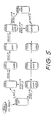
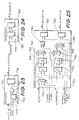
- the graphics engine 10 includes an input data bus 11, which provides a video input, and an output video data bus 19. Also included within the graphics engine 10 is a render processor (RP) interface 100, a run length controller 200, and a control unit 300.
- a data path includes interpolators 400 for each of red, green, and blue, a transparency interpolator 600 as well as compositors 500 for each of red, green, and blue and a matte combiner 700.
- An address generator 800 and a write controller 900 are also provided.
- Signal lines 14 provide for direct memory access (DMA) control.
- the control unit 300 accepts two clock signals 15 which include a pixel clock running typically at 13.35 MHz.
- the control unit 300 reads data from the RP interface 100, interprets those commands received, and passes the command operands to the run controller 200, and to the data path including interpolators 400.
- the command operands are also passed to the address generator 800 and the write controller 900.
- the control unit 300 is also responsible for decoding microcode from these commands, which is subsequently used by respective execution devices within the engine 10.
- the run controller 200 is initialised with the run length of the particular graphics command by the control unit 300 and produces a linearly increasing number in the form of a ramp from 0 to 255 for the duration of the run. This ramp is used by the interpolators 400 to control the mixing proportion in blend commands.
- the graphics engine 10 is configured to operate upon red, green, blue and matte (RGBM) information which is an industry standard.
- the colour data path of red, green and blue interpolators 400 in the general case of a blend command, is initialised by the control unit 300 with a start colour and an end colour.
- the colour data path produces a blend between these two colours, and then composites the result, including a percentage of the current colour, in the pixel memory (work screen store 30 or page store 4) via the RGBM out bus 19.
- the transparency data path includes a transparency interpolator 600 and a matte combiner 700.
- the transparency data path is initialised by the control unit 300 with a start transparency and an end transparency.
- the transparency data path produces a blend between these two values, and the result is used to control the compositing proportions in the colour components.
- the transparency blend can also be written or composited with the matte plane in the pixel memory.
- the address generator 800 provides the read and write addresses to pixel memory 4,30.
- the page memory 4 addresses are maintained independently from those of the work screen memory 30, allowing reads from the page memory 4, which is interconnected to the buses 11 and 19 via buffers, to occur in parallel with writes to the work screen memory 30, and visa versa.
- the write controller 900 provides synchronised read and write signals to the pixel memory 4,30.
- the write controller 900 provides a STALL signal to suspend operation in all execution units of the engine 10 when waiting for completion of read or write access to the work screen memory 30.
- the write controller 900 also maintains a pipeline of status signals which contains the micro-code used by other execution units.
- the data path as earlier described includes a colour portion divided into three component colours, red, green and blue. Each colour component is separated into two stages comprising an interpolator 400 and a compositor 500.
- the interpolators 400 are responsible for generating the blended colours, and the compositors 500 are responsible for mixing the blend with the pixel memory.
- the transparency portion of the data path also has an interpolator 600, but not a compositor.
- the green compositor 400 is used.
- the matte combiner 700 provides the colour compositors 500 with the mixing proportion which it selects from one of several possible transparency sources.
- the matte output is also fed to the red compositor 500 which allows the data which would have been written to the matte plane, to be written to the red plane instead.
- the control unit 300 preloads a set-up stage of a graphics command into the execution units even if the previous command is still being executed.
- the graphics instruction is initiated with a "START" signal.
- the data path 400/500 and the address generator 800 proceed in parallel and emit the first pixel after a minimum of six clock periods on the pixel clock PXCLK 15. A new pixel is thereafter emitted every clock cycle for the duration of the instruction unless stalled by a peripheral device connected to the engine 10.
- a ramp generator 150 (Fig. 10 to be described hereafter) within the run controller 200 supplies a linearly increasing number from 0 to 255 and indicates to the controller 300 when the instruction is completed via a "LAST" signal.
- the write controller 900 interfaces to the pixel memory 4,30, or the frame store 2, via the bus 21.
- the write controller 900 also interfaces to a further bus 20, supplying the pan/zoom engine 9 and workscreen memory 30, and keeps track of when and where to read and write pixels.
- compositing commands are the most common type of instruction given to the engine 10 and they allow the computer 1 to perform full colour linear blending operations in the page store 4 and on the screen 3 via the work screen store 30.
- Configuration commands are used to set up internal or external hardware connections prior to executing compositing commands.
- Synchronisation commands are used to keep the graphics engine 10 synchronised to internal hardware events or external hardware events. Table 1 shows the three types of instructions and their respective instruction codes.
- the source and destination of blending operations can be either the compositing page memory 4 (CM) or the workscreen 3 (WS). Accordingly, there are four types of compositing commands: compositing within the compositing memory 4; compositing within the workscreen memory 30; compositing from the compositing memory 4 to the workscreen memory 30; and compositing from the workscreen memory 30 to the compositing memory 4.
- CM to CM compositing one pixel is read and written in every pixel clock period (75 ns). Reads are performed in the first half of the pixel clock periods and writes in the second half.
- the graphics engine 10 uses a i pipeline delay system in which data is transferred sequentially between various devices within the engine 10. Accordingly, there is a delay between reading the "old" value of a pixel, and writing the "new" value of the pixel. For this reason, the compositing memory 4 address changes between the first and second halves of the pixel clock period.
- the compositing memory 4 Due to timing constraints in the compositing memory 4, there is one pixel clock period delay between issuing a read address, and reading the data at that address. This delay is compensated for by adjusting the position within the graphics engine 10 pipeline where the read data is received. The compositing memory 4 also has a one clock delay when writing pixel data, but this does not affect the internal operation of the graphics engine 10.
- a maximum of one pixel is read or written in every pixel clock period (75 ns). Reads are requested in one pixel clock period, and writes in another. Because of pipeline delays in the graphics engine 10, for the same reasons as described above, the workscreen memory 30 address changes between successive read and write requests.
- Handshake signals from the pan/zoom engine 9 indicate when the data is ready. This delay is compensated for by stalling the graphics engine 10 pipeline until the read data is received.
- the graphics engine 10 reads the data from the monitor or workscreen 3 in the clock period after the read acknowledge handshake signal is received from the pan/zoom engine 98e 8, in order to be compatible with the one clock delay in the compositing memory 4. Latches, (not illustrated and external to the graphics engine as earlier described), hold the data during this delay.
- the workscreen memory 30 can also have a delay when writing pixel data. Typically, the first pixel written will not be delayed, as the write request is "posted", and performed in subsequent clock periods.
- the pan/zoom ratio must be set to 1:1 for WS to WS compositing, as will be understood by those skilled in the art.
- CM to WS compositing is used to transfer pixel data from the compositing memory 4 to the workscreen memory 30.
- CM to WS compositing a maximum of one pixel is read and written in every pixel clock period. Reads are requested from the compositing memory 4 in the first half of the pixel clock period. Writes are requested from the workscreen memory 30 during the entire pixel clock period, but the address and data are only available in the second half of the pixel clock period. Separate addresses are maintained for the workscreen address and the compositing memory 4 address.
- CM to WS compositing can be used in conjunction with a reduction zoom ratio to reduce the size of the workscreen image.
- the pan/zoom engine 9 discards pixels from the graphics engine 10, and only writes every "NTH" pixel. This is transparent to the operation of the graphics engine 10, as the only difference it perceives is that writes appear to be completed quicker.
- CM to WS compositing can also be used in conjunction with a magnification zoom ratio to increase the size of the workscreen image.
- the pan/zoom engine 9 reads a pixel from the graphics engine 10, and writes the next "N x N" pixels with the same value. This is also transparent to the operation of the graphics engine 10, as the only perceived difference is that writes appear to take longer to complete. Note that only the first pixel address in a run is used by the pan/zoom engine 9. The graphics engine 10 generates addresses for subsequent pixels, but those addresses are not required by the current implementation of the pan/zoom engine 9.
- WS to CM compositing is used to transfer pixel data from the workscreen memory 30 to the compositing memory 4.
- a maximum of one pixel is read and written in every pixel clock period. Reads are requested from the workscreen memory 30 in the first half of the pixel clock period and writes are performed on the compositing memory 4 in the second half of the pixel clock period. If the workscreen read has not been acknowledged by the end of the pixel clock period, the pipeline will be stalled. The read request will remain pending, and the write to the compositing memory 4 will be repeated at the same address. Separate addresses are maintained for the workscreen memory 30 addresses and the compositing memory 4 addresses.
- WS to CM compositing can be used in conjunction with a reduction ratio to increase the size of the image as it is copied into the compositing memory 4.
- the pan/zoom engine 9 initialises a workscreen address during the first pixel in a run, but only increments this address after every "N" pixel read requests from the graphics engine 10. This has the effect of expanding each pixel, but is transparent to the operation of the graphics engine 10. Note that only the first pixel address in a run is used by the pan/zoom engine 9.
- the graphics engine 10 generates addresses for subsequent pixels, but these addresses do not take the reduction ratio into account.
- Configuration commands are used to set up internal and external hardware prior to executing compositing commands.
- the commands can be executed between compositing commands to allow long instruction streams to be formed.
- a Load Zoom ratio command passes a parameter word following the instruction to the pan/zoom engine 9 via the workscreen address bus.
- the expansion factor appears on bits 3 to 0 of the parameter, and the reduction factor appears on bits 7 to 4.
- Timing for the transfer is the same as for a WS write command and no pixels are written.
- the "run length" field of the load zoom ratio command is set to one. Table 2 shows the load zoom ratio parameters.
- a Load Graphics Engine (GE) Configuration command allows various modes to be set within the graphics engine 10. Ideally, these modes are contained within each graphics instruction. A limited number of bits within the instruction word, however, prevents this possibility. Table 3 shows the load GE configuration parameter.
- Bits 6 through 4 of the parameter following the load GE configuration instruction configure the "matte to red”, “matte to green”, and “matte to blue” modes respectively.
- Bits 3 to 0 of the parameter configure "write enables" to the R,G,B and M planes of the workscreen memory 30. These write enables provide a way to disable writes to individual planes in the workscreen memory 30. Compositing memory 4 writes are not affected by these bits. Image and matte write enables in graphics instructions can also disable writes, but not to individual planes.
- Bits 6 through 0 are used to allow data which is normally written to the matte plane, to be written to the red plane.
- Bits 10 through 7 allow screen compositing operations to be sped-up in certain circumstances.
- the SBW bit enables a "skip bit matte writes” mode. This mode disables screen write requests, when the appropriate bit in the bit map mask is 0, rather than simply disabling the screen plane write enables.
- the SER and SEW bits assert the start on every read, or the start on every write function.
- the "run length" field of the load configuration command should be set to one.
- a Load Register command allows most of the internal registers of the graphics engine 10 to be loaded individually or collectively.
- the configuration of the load register instruction is shown in Table 4. This command is used in conjunction with the "execute microcode" instruction for testing purposes. Bits 27 through 0 of the instruction specify which internalregister is to be loaded. The parameter following the instruction is then loaded into the specific register. More than one register can be loaded with the parameter. For example, registers 0 to 3, as defined in table 4, can be loaded at the same time because each register uses different bits from the parameter. Typically, the "alt microcode" register would also be loaded, before the "execute microcode" instruction is issued.
- Run Length and Texture Offset registers cannot be loaded using the load register command. Separate registers called “alt run length” and “alt texture offset” registers, however, can be loaded.
- the graphics pipeline uses these registers instead of the usual registers when the "execute microcode" instruction is executed. Table 5 provides a description of various registers provided within the graphics engine 10.
- Synchronisation commands are used to maintain the graphics engine 10 synchronised to internal and external hardware events. There are two synchronisation commands, namely no operation (NOP) and WAIT.
- NOP no operation
- WAIT WAIT
- the NOP instruction has no effect upon the graphics pipeline other than to consume one word and one clock cycle. It is intended to be used at the end of an instruction stream so that the length of the stream is a multiple of four 32-bit words. This ensures that the DMA controller, provided on bus 14 in Fig. 2, and which transfers data in four word bursts, will always send the last command.
- the WAIT instruction prevents the graphics engine 10 from executing new instructions until one of three events occur. Those events are: a hardware restart signal is received, a software restart is received, or the graphics pipeline becomes empty. Options to the instructions select which of the events will restart instruction execution. Pixels from the previous instruction which are still in the graphics pipeline, are not effected by this instruction.
- the hardware restart option allows the graphics engine 10 instruction execution to be synchronised to external "real-time” events. This is required when performing a "test scan” where the graphics engine 10 is used to copy an image from the compositing memory 4 to the workscreen 3, while the scanner 6 is writing to the page memory 4 simultaneously.
- the graphics engine 10 and the scanner 6 operate on opposite halves of the page memory 4, and swap over every eight lines.
- the instruction stream presented to the graphics engine 10 is separated into multiple strips of eight lines. A single WAIT instruction is inserted between the compositing commands for each strip. This forces the graphics engine 10 to wait for the scanner to "catch-up" before proceeding to the next step.
- a software restart option allows the computer 1 to be synchronised to the graphics engine 10 instruction execution. If the computer 1 needs to perform certain tasks between groups of graphics instructions, a WAIT instruction can be inserted between the groups. When the graphics engine 10 reaches the WAIT, an interrupt is optionally generated, and the execution of the new instructions is suspended until the computer 1 writes to a CONTROL register with the RESTART bit set, as will be discussed later.
- the pipeline empty restart option allows the graphics engine 10 to wait-until the previous instruction is fully completed before starting a new instruction.
- This instruction is generally not required in normal operation. It is only required if a design error allowed neighbouring i instructions to effect each other.
- Table 6 shows the bit relationship of the WAIT instruction.
- registers are also available for the computer 1 to interface with the graphics engine 10. Table 7 lists internal registers of the graphics engine 10 showing the relative address, size and whether the respective address is readable or writable.
- the COMMAND register provides an alternate mechanism for writing graphics commands to the graphics engine 10. Writing to the COMMAND register places the input data on the top of a FIFO 150 within the RP interface 100, and is effectively the same as writing via the DMA bus 14. The status of the FIFO 150 should be read from the STATUS register before writing to the-COMMAND register, to ensure that the FIFO 150 is not full. Writing graphics commands via the COMMAND register is relatively slow, as it is not expected to be used in normal operation.
- the FIFO 150 can also be written one word at a time.
- the control unit 300 does not read the FIFO 150 until it contains at least four words.
- Table 8 shows the arrangement of the command register.
- the CONTROL register is used for setting interrupt masks, clearing interrupts, and enabling various test modes, and includes a bit configuration as shown in Table 9.
- the HIE bit is the hardware interrupt enable. If set to a 1, the computer 1 will receive an interrupt when the graphics engine 10 receives a WAIT command when the "hardware restart" option is enabled. This interrupt is cleared by writing a 1 to the CHI bit (even if the graphics engine 10 is stopped). The setting of the HIE bit can be read from the STATUS register.
- the EIE bit is the "ERROR" interrupt enable. If set to a 1, the computer 1 will receive an interrupt when the graphics engine 10 detects an error condition. This interrupt is cleared by writing a 1 to the CEI bit, until a new error is detected. An error is detected if a hardware restart or a software restart is received when the graphics engine 10 is not in the STOPPED state. In the case of a hardware restart, this indicates a loss of synchronisation with the external real time event.
- the current setting of the EIE bit can be read from the STATUS register.
- the RST bit is used to restart the graphics pipeline. When this bit changes from a 0 to a 1, the graphics pipeline is restarted.
- the SWR bit is used to generate a software reset. When set to a 1, the entire graphics engine 10 is reset to the power on reset condition. The SWR bit does not need to be cleared by a programmer, as the CONTROL register is also reset.
- the SEE bit is the "stop on error” enable. If set to a 1, the graphics engine 10 will enter the STOPPED condition if an error is detected.
- TMO is used to put the run length counter 220 into a test mode as will be discussed later.
- TM1 is used to put page and screen address counters, within the address generator 800 into a test mode, as will also be discussed later.
- the STATUS register is used to monitor the interrupt flags and the FIFO 150 status, to read the version number, and to read the status of the various test modules.
- Table 9 shows the configuration of the status register.
- the HIE, SIE and EIE bits reflect the state of the interrupt masks set in the CONTROL register.
- the HIF, SIF, and EIF bits are interrupt flags. If these flags are set, and their corresponding interrupt enable bit is set, an interrupt will be generated.
- the HIF bit is set when the graphics engine 10 receives a WAIT command with the "hardware restart” option enable. This bit is cleared by writing a 1 to the CHI bit in the CONTROL register.
- the SIF bit is set when the graphics engine 10 receives a WAIT command with the "software restart” option enable. This bit is cleared by writing a 1 to the CSI bit in the CONTROL register.
- the EIE bit is set when an error condition is detected. This interrupt is cleared by writing a 1 to the CEI bit in the CONTROL register.
- the FFF bit is set when the FIFO 150 is full, indicating that the COMMAND register should not be written.
- the GR bit is set when the graphics engine 10 is running. Running is defined as "not waiting and the FIFO 150 is not empty”. (i.e. when the graphics engine 10 is executing an instruction).
- the DOE bit is set when a DMA controller, with the RP controller 120, detects an overrun condition in the FIFO 150.
- the TSn bits reflect the level of a number of internal modes which are used during testing by the device manufacturer during manufacture of the graphics engine 10 using LSI technology.
- the Vn bits contain the version number of the integrated circuit (LSI) chip.
- the graphics engine 10 inputs and outputs can be classified into four categories:
- Table 10 provides a list of each of these signals.
- the computer 1 can access the graphics engine 10 in three ways, either by DMA writes, register reads, and register writes.
- the DMA interface 14 is used to transfer graphics commands from the memory of the computer 1 at high speed. Register writes are used to configure the graphics engine 10, and register reads are used to monitor the status of the graphics engine 10. Register reads and writes are also used in test and debug modes.
- the graphics engine 10 has an internal FIFO 150 which accepts four consecutive 32-bit words from the DMA controller of the computer 1 in a single DMA transfer. This type of transfer is known as a "quad word burst flyby" DMA transfer.
- a DMA request is issued by the graphics engine 10 whenever the FIFO 150 has room for at least four 32-bit words.
- the DMA controller of the computer 1 subsequently acknowledges the request and writes four 32-bit words of data in a single burst transfer.
- the time to complete the transfer is determined by the access time of the memory (usually dynamic RAM) of the computer 1.
- the time between accesses is determined by the available bandwidth of the bus interconnecting the computer 1 and graphics engine 10). If no other DMA channels are operating, the graphics engine 10 is guaranteed at least 50% access to this bus. Assuming most accesses to the computer 1 are burst accesses, the peak transfer rate to the graphics engine 10 is approximately 432-bit words every 26 processor clock cycles. This is equal to five million full colour pixels per second, or 20 megabytes per second at 33MHz when using the i960 processor.
- Registers are written by the computer 1 using the 32 bit data bus 12, one address line, a read/write signal, and a chip select as indicated by the bus 13 in Fig. 2.
- the interface between the graphics engine 10 and the compositing page memory 4 preferably has a bandwidth of approximately 100 megabytes per second.
- One 32-bit pixel is read and written in every pixel clock period (75 ns). Reads are performed in the first half of the pixel clock periods, and writes in the second half.
- the data bus 19 changes direction twice in every pixel clock period. Since the width of the data bus 19 is high (32 bits) care must be taken to ensure that there is no contention between the graphics engine 10 and the compositing memory q when the bus 19 is changed from input to output, and output to input.
- the compositing memory 4 uses static RAM chips with an access time of 25 ns. In order to relax timing constraints on the graphics engine 10, a one clock delay is inserted between issuing a read address, and reading the data at that address. This delay is compensated for by adjusting the position within the graphics pipeline of the engine 10 at which the data is accepted.
- a one clock delay is inserted between issuing a write, and when the write is actually performed. This delay is transparent to the operation of the graphics engine 10.
- the interface between the graphics engine 10 and the workscreen 3 uses the same address and data bus as used to read and write to the compositing memory 4.
- the workscreen memory 30 is shared between an S Bus device, display refresh, and reads and writes from the graphics engine 10 via the pan/zoom engine 9. As a result, there is a delay between issuing a read request, and reading the data at that address. Handshake signals from the pan/zoom engine 9 indicate when the data is ready. This delay is accounted for by stalling the pipeline of the graphics engine 10 until the read data is received.
- the workscreen memory 30 can also have a delay when writing pixel data. Typically, the first pixel written will not be delayed, as the write request is posted, and performed in subsequent clock periods.
- the render processor interface 100 of Fig. 3 is responsible for controlling and monitoring the status of the graphics pipeline of the engine 10 from the computer 1 which is preferably an i960 processor. All control signals between the graphics engine 10 and the computer 1 are synchronous to the computer clock HCLK.
- the RP interface 100 resynchronises the signals to the pixel clock (PXCLK) which is used by the remainder of the graphics engine 10.
- the RP interface 100 is divided into a control block 120 and a first-in-first-out shift register (FIFO) 150.
- the RP controller 120 is not shown in detail but generally includes an address decoder, a control register, a status register, an interrupt controller and a DMA controller.
- the address decoder generates register select signals for the control register, the status register and the command register.
- the control register when selected by the address decoder is loaded with data from the computer 1 which is used to configure the interrupt, synchronisation, and test modes as earlier defined.
- the control register contains resynchronisation flip-flops to synchronise to the pixel clock PXCLK.
- the status register allows the computer 1 to monitor interrupt flags, the status of the FIFO 150, and other internal conditions as defined earlier.
- the status register also contains circuitry to regenerate synchronised reset signals and status outputs.
- the interrupt controller combines interrupt flags from the status register where the interrupt enables from the control register to produce the output INT of i the interface 100.
- the DMA controller generates a DMA request when ROOM_44, seen in Fig. 3, indicates that the FIFO 150 has room for four more words from the computer 1.
- ROOM_44 seen in Fig. 3
- a new word is written into the FIFO 150 in each processor clock period where NEXT is asserted. If a DMA acknowledge is received when a DMA cycle has not been requested, an error condition is generated.
- a WRITEFF signal is asserted for each valid DMA word.
- the FIFO 150 as seen in Fig. 4 uses an eight word 32 bit dual port RAM 170 to interface the computer 1 with the pixel pipeline within the engine 10.
- a write address generator 155 synchronised to the processer clock PLCK interfaces the computer 1 to the RAM 170.
- a read address generator 160 synchronised to the pixel clock PXCLK interfaces the RAM 170 to the pixel pipeline. Handshake signals between the two address generators are synchronised in each of their respective receiving circuits.
- the write address generator 155 operates synchronously with the i processer clock PCLK to produce an address and a write pulse to the RAM 170.
- the generator 155 also generates a signal to indicate when there is room for four more words, and two signals to indicate when the two halves of the FIFO 150 contain valid data.
- the FFMT output provides an indication to the computer 1 via the status register of the RP Controller 120 that the COMMAND register should not be written.
- the generator 155 is implemented with a three-bit counter which is reset to 0 when the RP_RESET signal is asserted. The counter increments when the WRITE_FF signal is asserted.
- the read address generator 160 operates synchronously with the pixel clock PXCLK to produce an address to the RAM 170.
- the generator 160 provides a signal to indicate when the FIFO 150 is empty and two signals to indicate when the two halves of the FIFO 150 have been read.
- the generator 160 is implemented with a four-bit state machine which is initialized when the PX_RESET signal is asserted.
- Fig. 5 shows a state transition diagram which illustrates how the address and the "empty" signal (MT) are generated within the read address generator 160.
- the control unit 300 interfaces the render processer FIFO 150 to the graphics pipeline.
- the unit 300 consists of instruction and microcode registers 305 and 310, an instruction interpreter 320, and an instruction decoder 350.
- the instruction interpreter 320 parses incoming instructions and parameters, loading the registers 305 and 310 in accordance with the command received.
- the instruction decoder 350 uses the instruction register 310 to produce a status word which is passed to the graphics pipeline. If an "EX_UCODE" instruction is detected, the normal instruction decode is bypassed by the data in the micro-code register 305. This code is used for test and debug purposes.
- instruction interpreter 320 and instruction decoder 350 will be apparent to those skilled in the development of applications specific microcontrollers and processors. the development of each new microcontroller, a new or modified instruction set must be developed which when reading data, must involve the interpretation and decoding of various commands.
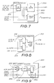
- the run controller 200 interconnects the RP interface 100 with the data path including interpolators 400 and compositors 500.
- the run controller 200 performs two tasks through the generation of an interpolation ramp, and to indicate when the last pixel in a run is being composited. To perform these functions, it is required that the run controller 200 be loaded with the run length, a start pulse, a valid indicator, and a stall indicator.
- the run length is loaded from the FIFO 150 database when instructed by the instruction interpreter 320 of the control unit 300.
- the start and valid signals also come from the instruction interpreter 320 whilst the stall signal comes from the write controller 900.
- the run controller 200 includes a run length register 210, a run length counter 220, and a ramp generator 250.
- the run length register 210 shown in more detail in Fig. 8, includes latches 212 and 214 and a multiplexer 216.
- the latch 212 contains the run length of the next graphics command. The current graphics command can still be running when the latch 212 is loaded.
- the latch 214 contains an alternate run length which is used when an USE_ALT signal is asserted.
- the run length counter 220 includes a multiplexer 222, a decrementing counter 224, a gate 226, a latch 228 and a logic unit 230.
- the run length counter 220 counts the number of pixel composited and indicates when the last pixel is in progress.
- the counter 220 is initialized with one less than the value in the run length register 210 when the START signal is asserted.
- the counter 220 decrements in all cycles, including the start cycle, unless STALL is asserted or VALID is negated, in which case the counter retains the current value.
- the LAST signal is asserted.
- the minimum value for the run length is 1. In this case, the LAST signal is asserted in the same state as the START signal is asserted.
- the ramp generator 250 seen in Fig. 10 generates a linearly increasing number from 0 to 255 over the real time duration of the graphics instruction being executed.
- the generator 250 is initialized with the value in the run length register 210 when the START signal is asserted.
- the generator 250 is updated in all cycles unless the STALL signal is asserted.
- the ramp generator 250 comprises an input latch 252 which supplies a multiplexer switch 254 selected by the START signal.
- the multiplexer 254 outputs the 13 bit data word, representing the run length, to four individual units which operate on selective bits of the word.
- the eight least significant bits are supplied to a ROM 260 which comprises a lookup table outputting a value corresponding to 255/(RL-1). All 13 bits of the word are supplied to a subtractor CONSTl 265 which calculates the value (511 - RL). Similarly, all 13 bits also supply a further subtractor CONST2 270 which calculates (512 - 2RL).
- the five most significant bits supply a mode detector circuit 275 which represents a five input OR gate which provides a jump signal.
- the outputs of ROM 260, CONSTl 265 and CONST2 270 connect to three multiplexer switches 284, 280 and 282 respectively.
- the multiplexers 280 and 284 are switched when the jump output of the mode detected circuit 275 is asserted.
- the multiplexer 282 is switched when the most significant bit output from the accumulator D-flipflop 292 is asserted.
- the generator 250 also includes a summer 290, further multiplexers 286 and 288, a flipflop 294 and a latch 296. It is apparent from Fig. 10 that the output of the accumulator flipflop 292 divides such that all 16 bits are fed back to the summer 290, with the eight most significant bits outputting to the multiplexer 288. As indicated earlier, the most significant bit, bit 15, feeds back to switch the multiplexer 282 as well as supplying an input to the flipflop 294.
- Figs. 11A and B show the two ways in which the ramp output of the generator 250 is formed. Note that an update of the generator 250 does not necessarily imply that the ramp output value is changed (as in the case when the run length is greater than 255).
- the generator 250 operates in two modes. Firstly a "jump" mode when the run length is less than or equal to 255, and a "step” mode when the run length is greater than 255. The mode is determined by an examination of the five most significant bits of the run length. In the jump mode, the ramp value will increase by at least one in every clock period. In the step mode, the ramp value increases by a maximum of one in each clock period.
- the output value from the ROM 260 is added to the accumulator 292 which is initialized to zero by the START signal.
- the most significant bits of the accumulator form the ramp output as can be seen from Fig. 10.
- the generator 250 applies an algorithm similar to Bresenham's line drawing algorithm, which is known to those in the computer graphic arts.
- the accumulator 292 is initialized with the constant (511 - RL), and the ramp counter is initialized to zero. In subsequent clocks, one of two constants are added to the accumulator:- 510 if the accumulator is negative, or, (512 - 2RL) if the accumulator is positive.
- the ramp counter flip flop 294) is incremented on every clock where the accumulator 292 is positive. Note that thestep mode requires the multiplexer 254 to bypass the latch 252 during the START cycle. This allows the new value in the CONSTl module 265 to be loaded into the accumulator 292 in the START cycle.
- the multiplexers 280 and 282 are shown in Fig. 10 for clarity only. A simpler implementation for the multiplexer 280 is a string of AND gates. Similarly, the multiplexer 282 can be implemented as a string of OR gate for the nine least significant bits, and a string of AND gates for the most significant bits.
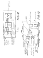
- the colour component data path of the graphic engine 10 consists of three eight-bit data paths. Each eight-bit path contains an interpolator 400, which also performs colour correction, and a compositor 500.
- the red, green and blue interpolators are identical. The three compositors, however, are slightly different. The green compositor is used by the matte channel in some instructions and the resulting differences in the green channel are described later in this specification.
- the colour interpolators 400 comprise three modules: a synchronisation module 410, an interpolation phase A 420, and an interpolation phase B 450.
- the synchronisation module 410 spans stages 0 and 1 of the graphics pipeline and holds operands for the current instruction, and instruction operands for the next instruction.
- the interpolation phases A and B (420 and 450) perform blends and colour correction. The two phases are required in order to maintain one pixel per clock cycle. Phase A (420) is in stage 2 of the pipeline, and phase B (450) is in stage 3.
- the synchronisation module 410 is not shown in detail but however comprises latches and flipflops which provide the start colour, the end colour and the pixel value.
- the interpolation phase A 420 is shown in Fig. 13 and performs two types of calculations, either blends, or colour corrections. Those skilled in the art will appreciate that colour runs are simply a degenerate case of a blend when the start and end colours are the same.
- the interpolator phase A420 comprises a summer 4Z2 which subtracts the START value from the END value.
- the multiplexers 424 and 426 change the inputs to the multiplier 430 respectively.
- the summer 422 has a nine-bit two's complement output which is fed to the multiplier 430.
- the END value (which also corresponds to the CONTRAST) is fed to the multiplier 430 when the sign bit is set positive.
- the second input of the multiplier 430 comes from the ramp generator 250 of Fig. 10 and has the effect of controlling the mixing proportion.
- the second input of the multiplier 430 comes from the commands pixel string. A new pixel to be colour corrected is loaded every non-stalled clock period. Only the top nine bits and the sign of the multiplier output are required. The output is a 10-bit two's complement number. Rounding is not performed as a one least significant bit error is considered acceptable.
- the START_D output contains a delayed version of the START value for the next phase of the interpolator.
- the START value is equivalent to the BRIGHTNESS.
- the phase B circuit 450 comprises two multiplexers 452 and 454 both supplying a summer 458.
- the summer 458 supplies a limiter 460 which, in turn, supplies the output via a latch 462.
- the multiplexer 452 changes the inputs to the adder 458 to perform the multiplication by 2 for the colour correction function.
- the most significant bits pass straight through to the adder 458. For blend commands, this has the effect of signextending bit 8 by one position.
- the multiplexer 454 adds an extra two inputs to the adder 458 to perform a sign-extension for the colour correction function, which uses a 8-bit signed format for the BRIGHTNESS. For blend commands, these two bits are set to 0, as the START value is unsigned.
- the adder 458 sums the two 10-bit signed numbers output from the multiplexes 452 and 454 to produce a 10-bit signed result, and a positive overflow indicator (POV).
- POV positive overflow indicator
- a negative overflow is not possible in either blend or colour correction modes. In blend mode, the start value is always positive, and in colour correction mode, the MULT value is always positive.
- the adder 458 output is passed to the limiter 460 which is used to saturate values greater than 255 to 255, and values less than 0 to 0. This function can be disabled by an EFFECTS signal which comes from the COLOUR SOURCE field in the command.
- the limiter 460 has no effect in run or blend commands as the adder 458 output is always in the range 0 ... 255.
- the output from the limiter 460 is latched (462) in every non-stalled clock period, in readiness for the next pipeline stage.
- the limiter 460 is not shown in detail as its configuration can be readily derived from the above description.
- the limiter 460 has an input bus range from -128 to +638.
- Fig. 15 shows a colour compositer 500 which includes four modules comprising a synchronisation module 520, a compositing phase A 540, a compositing phase B 560, and a matte multiplexer 580.
- the synchronisation module 520 is in stage 4 of the graphics pipeline. It latches the RGBM data from the external compositing or workscreen memory (28 or 30) and synchronises it with the pixel pipeline.
- Compositing phases A and B 540 , and 560 perform a blend between the original value in the external memory, and the new value from the corresponding interpolator 400.
- the proportion between original and new is controlled by the BLEND bus, which comes from the matte combiner 700. Two phases are again required in order to maintain one pixel per clock cycle phase.
- Phase A540 is in stage 5 of the graphics pipeline and phase B 560 is in stage 6.
- the matte multiplexer 580 allows the data from the matte channel to be output on one or more of the colour planes. This is performed in stage 7 of the pipeline.
- the G OUT bus is shown shaded as it only exists in the green channel for use with the matte combiner 700.
- the synchronisation module 520 is not shown in detail as it merely latches data from external memories to provide that data synchronously with the phase A unit 540.
- the STALL signal is delayed in this module by one clock period to compensate for the one clock delay when reading from the compositing or workscreen memory 28 or 30 as earlier noted.
- Phase A 540 includes a summer 542, a multiplier 546 and output latches 548 and 550. All commands use the same format with 8-bit unsigned . values on each of the NEW, ORIG, and BLEND inputs.
- the second input to the multiplier 546 comes from the matte combiner 700 and has the effect of controlling the mixing proportion.
- a value of 0 represents a fully opaque compositing. Only the top 8 bits and the sign of the multiplier 456 output are required. The output is a 9-bit two's complement number. Rounding is again not performed as a one least significant bit error is considered acceptable.
- the NEW_D output contains , a delayed version of the NEW value for the next phase (560) of the compositor 500.
- Phase B 560 includes an adder 562 which sums the 9-bit signed number from the multiplier S46 in phase A with the 8-bit unsigned value from the ORIG delay flip-flop 550 also in phase A 540. The result is always in the range 0 to 255 as the compositor 500 can only produce numbers between the ORIG and NEW values.
- the output from the adder 562 is accepted by latch 564 in every non-stalled clock period, in readiness for the output stage of the pipeline.
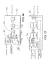
- the transparency data path seen in Fig. 2 comprises a transparency interpolator 600 and a matte combiner 700. That data path performs two main functions, firstly to generate a transparency blend by interpolating between a START and END transparency, and to combine the transparency blend with the matte plane.
- the transparency interpolator 600 is shown in Fig. 18 having three modules including a synchronisation module 610, an interpolation phase A 640, and an interpolation phase B 670.
- the synchronisation module 610 spans stages 0 and 1 of the pipeline. It holds operands for the current instruction, and latches operands for the next instruction.
- Phases A 640 and B 670 perform transparency blends and texturing. Again two phases are required in order to maintain one pixel per clock cycle. Phase A is in stage 2 of the pipeline and phase B is in stage 3.
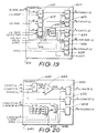
- Fig. 19 shows the various components within the synchronisation module 610.
- Latches 612 and 614 hold the START and END transparency parameters for the next instruction. This corresponds to stage 0 of the pipeline.
- Flip flops-620 and 622 load these values when the START signal indicates the first pixel of a new instruction is in progress.
- a third latch-616 holds the texture start parameter for the next instruction. This is a 2-bit parameter which determines the byte offset into the initial texture word for texture run and blend commands. It is loaded into a third flip-flop 624 via a next offset module 618 when the START signal indicates' the first pixel of an new instruction is in progress.
- a fourth flip-flop 626 holds the texture for up to four pixels in texture run and blend commands. The flip-flop 626 is loaded from the data bus D_IN in every fourth non-stalled clock period.
- a fifth flip-flop 628 holds the transparency for each pixel value in pixel string commands, and is loaded from the data bus in every non-stalled clock period
- the next offset module 618 is used to control the texture byte offset, and the texture word flip-flop 626.
- the texture byte offset is initialised when the START signal is asserted, and counts by one in other non-stalled clock periods. When the offset equals 3, the LASTT signal is asserted.
- the texture word flip-flop 626 enable signal is also asserted at this time as well as during the start cycle
- Phase A 640 includes a summer 642 configured to subtract two input data bytes.
- the output of the summer 642 is a 9-bit two's complement output which is fed to a multiplier 644.
- the second input of the multiplier 644 comes from the ramp generator 150 of Fig. 10 and has the effect of controlling the mixing proportion between the start and end values. Only the top eight bits and the sign of the multiplier 644 output are required. ,The output is a 9-bit two's complement number. Again, rounding is not performed as one least significant bit error is considered acceptable.
- Phase A 640 also has a T_START_D output which contains a delayed version of the T_START value provided by a latch 652 for the next phase of the interpolator 600.
- a multiplexer 646 uses the T_OFF signal from the synchroniser 610 to select one of the four texture bytes in the T_PIXELS input. In texture run and blend commands, a different byte is selected in each pixel clock PXCLK period. In pixel string commands, the transparency is selected from the T_PIXELS input via a second multiplexer 648. The texture is latched (654) to maintain synchronisation with pipeline stage 2.
- an adder 672 sums the 9-bit signed value from the multiplier 644 in Fig. 20 with the 8-bit start value. The result is always a positive 8-bit value since it must be in the range T_START ... T_END.
- a multiplexer 676 selects the output of the adder 672 for run or blend commands, or the texture byte for other commands. In bitmap commands, and commands which do not have subsequent words, the opaque signal is asserted. This has the effect of forcing the texture to 25S (opaque).
- the output from the multiplexer 676 is latched (678) in every non-stalled clock period, in readiness for the next pipeline stage.
- the transparency value from the output of the "opaqueing" module is also latched (680) and passed separately to the matte combiner 700.
- the matte combiner 700 is shown in Fig. 22 having four modules including a synchronisation module 710, a matte calculator 730, a matte delay 720, and a green multiplexer 790.
- the synchronisation module 710 is in stage 4 of the pipeline. It latches the matte plane of the RGBM data from the external compositing 4 or workscreen 30 memory in the first half of the pixel clock period. Based on this value and the transparency from the transparency interpolator 600, the matte calculator 730 produces a blend value for the colour compositors 500, and a new matte value for the compositing memory 28. Matte calculations are performed in stage 4 of the pipeline.
- the delay 720 passes the matte value unchanged to the green multiplexer 790 to synchronise with the colour components which are calculated in stages 5 and 6.
- the green multiplexer 790 allows the data from the green channel (400, 500: Fig. 2) to be output on the matte plane of the compositing memory 4. This is performed in stage 7 of the pipeline.
- Fig. 23 shows the components within the matte synchronisation module 710.
- a latch 712 produces a delayed version of the STALL signal to compensate for the one clock delay in the compositing memory 28.
- the input data from the external memory is asynchronous to the main internal pixel clock PXCLK. It is, however, synchronous to the CLK 2 signal which is used to derive the pixel clock via a NAND gate 714, so the phase is fixed. This data is latched (716) in the first half of the pipeline stage 4.
- Both the TR_IN and the M_SYNCD inputs are 8-bit unsigned values.
- the components in the top half of Fig. 25 calculate the BLEND output which is used to control the mixing proportion in the colour compositors 500. input to this block with a value of 0 represents fully transparent compositing. An output value of 0, however, represents fully opaque compositing.
- the BLEND value is calculated by substracting, using an adder 734, the matte data in the compositing (or workscreen) memory 28 from the transparency which has either a run, blend or texture value.
- a limiter 738 saturates this value to 0 if the result is negative, as indicated by the carry bit from the adder 734.
- a multiplexer 742 can bypass this calculation and select the input transparency if the T_MINUS_M input is not asserted (the T_MINUS_M signal is decoded from the command word in the control unit 300.) To compensate for the different input and output sense of the transparency, the multiplexer 742 is normally inverted by an EXOR block 750, or is passed straight through to the output via a latch 752 when the T_INV signal is asserted.
- the components in the bottom half of Fig. 25 calculate the M_OUT output which is written into the matte plane. This value is calculated by subtracting, using an adder 736, the transparency from the matte data in the compositing (or workscreen) memory 4,30. A further limiter 740 saturates this value to 0 if the result is negative, as indicated by a carry from the adder 736. A subsequent multiplexer 746 can bypass this calculation and select the input transparency if the M_MINUS_T input is not asserted. A further multiplexer 748 selects the SUBS_T value if the matte source field of the instruction specifies "subsequent". Both the BLEND M_OUT VALUES are latched to synchronise to stage 4 of the pipeline;
- the matte delay 720 passes the matte value unchanged to the green multiplexer 790 to synchronise with the components which are calculated in stage 5 and 6.
- a flip-flop 722 synchronises to stage 5, and a second flip-flop-754 synchronises to stage 6.
- the address generator block 800 of Fig. 2 is responsible for providing read and write addresses for the compositing memory 4 and the workscreen memory 30. A read cycle and a write cycle are performed in each pixel clock period. Compositing memory 4 addresses are provided by a page - address generator within the address generator 800, and workscreen addresses are provided by a screen address generator also within the generator 800.
- the address generator 800 operates in a manner known to those skilled in the art in selecting appropriate addresses within the workscreen and compositing memories. Having selected the appropriate address, either the page or screen addresses are multiplexed as determined by read and write signals.
- the write addresses are passed through a five stage delay to compensate for delays through the colour and transparency data paths.
- the write controller 900 of Fig. 2 performs three main tasks, namely:
- the write controller 900 forms functions known to those skilled in the art and a detailed explanation is not required in the specification. Essentially, the write controller 900 includes three stages comprising a bit map shift, a status delay, and an I/O control unit. In bit map mode instructions, a single 32-bit word is used to enable or disable writes for up to 32 consecutive pixels.
- the status delay module provides appropriate pipeline delays of write control and other status information. It also contains a block which is used to detect when the pipeline is empty.
- the I10 controller interfaces to the compositing memory 4 and the pan/zoom engine 9 handshake signals.
- the preferred embodiment of the graphics engine is able to implement a wide range of commands so as to manipulate image data.
- Five such commands respectively known as CANVAS RUN, CANVAS BLEND, CANVAS PIXELS, CANVAS TEXTURE RUN and CANVAS TEXTURE BLEND will now be described.
- the CANVAS RUN function composites a run of colours with the image, with compositing controlled by the transparency and the matte plane.
- This command simulates the interaction of paint with canvas or other textured materials, as textured dents in the background progressively "fill up” with "paint".
- the canvas run command composites the run length number of pixels of a colour equal to the start colour, starting at the page address.
- the intensity of compositing is controlled by the difference between the transparency run and the matte plane of the image.
- the matte plane is changed to be the difference between the matte value and the run transparency.
- the canvas run command is used for compositing object based constant colour "brush strokes" onto a textured background, where it is desirable to simulate the cumulative interaction between paint and a textured background.
- the page matte should contain an image which corresponds to the texture of the background.
- the CANVAS BLEND function composites a blend of colours with the image, with compositing controlled by the blend transparency and the matte plane. This command simulates the interaction of paint with canvas or other textured materials, as textured dents in the background progressively "fill up” with "paint".
- the canvas blend command composites the run length number of pixels of a colour smoothly changing from the start colour to the end colour with the image, starting at the page address.
- the intensity of compositing is controlled by the difference between the blended transparency and the matte plane of the image.
- the matte plane is changed to be the difference between the matte value and the blend transparency.
- the canvas blend command is used for compositing object based blended colour "brush strokes" onto a textured background, where it is desirable to simulate the cumulative interaction between paint and a textured background.
- the page matte should contain an image which corresponds to the texture of the background.
- the CANVAS PIXELS function composites a run of pixels with the image, with compositing controlled by the pixel transparency and the matte plane. This command simulates the interaction of paint with canvas or other textured materials, as textured dents in the background progressively "fill up” with "paint".
- the canvas pixels command composites the run length number of pixels with the image, starting at the page address.
- the intensity of compositing is controlled by the difference between the pixel transparency and the matte plane of the image.
- the matte plane is changed to be the difference between the matte value and the pixel transparency.
- RGB (colour corrected) [n] Limit((RGB(contrast)*RGB(pixel)[n])/256+ RGB(bright))
- the canvas pixels command is used for compositing pixel based "brush strokes" onto a textured background, where it is desirable to simulate cumulative interaction between paint and a textured background.
- the page matte should contain an image which corresponds to the texture of the background. This command can also be used for simulating screen printing of a natural image onto a textured background.
- the CANVAS TEXTURE RUN function composites a run of colours with the image, with compositing controlled by the texture and the matte plane. This command simulates the interaction of textured brush strokes with canvas or other textured materials, as textured dents in the background progressively "fill up” with "paint".
- the canvas run command composites the run length number of pixels of a colour equal to the start colour, starting at the page address.
- the intensity of compositing is controlled by the difference between the i subsequent texture bytes and the matte plane of the image i
- the matte plane is changed to be the difference between the matte value and the texture bytes.
- the canvas texture run command is used for compositing textured object based constant colour "brush strokes" onto a textured background, where it is desirable to simulate the cumulative interaction between paint and a textured background.
- the page matte should contain an image which corresponds to the texture of the background, and the subsequent texture bytes should contain a texture which relates to the texture of the paint medium.
- the CANVAS TEXTURE BLEND function composites a blend of colours with the image, with compositing controlled by the texture and the matte plane. This command simulates the interaction of textured brush strokes with canvas or other textured materials, as textured dents in the background progressively "fill up” with "paint".
- the canvas blend command composites the run length number of pixels of a colour smoothly changing from the start colour to the end colour with the image.
- the intensity of compositing is controlled by the difference between the subsequent texture bytes and the matte plane of the image.
- the transparency values of the start and end colour are ignored.
- the matte plane is changed to be the difference between the matte value and the texture bytes.
- the canvas texture blend command is used for compositing textured object based constant colour "Brush strokes" onto a textured background, where it is desirable to simulate the cumulative interaction between paint and a textured background.
- the page matte should contain an image which corresponds to the texture of the background, and the subsequent texture bytes should contain a texture which relates to the texture of the paint medium.
- many of the individual building blocks described include a latch or latches which are used to buffer data out of that respective unit.
- Those latches are only used in the present embodiment to enable synchronisation throughout the various pipeline stages through the graphics engine 10. With hardware that is capable of operating at much higher speeds, the processing delays within the various hardware items will become insignificant and the requirement for the latches will no longer be necessary.
Description
- Figs. 1A-1F are schematic block diagrams of prior art image manipulation systems which incorporate a graphics engine;
- Fig. 2 is a schematic block diagram of the preferred embodiment of the graphics engine;
- Fig. 3 is a schematic block diagram of the render processor interface of Fig. 2;
- Fig. 4 is a schematic block diagram of the first-in-first-out register of Fig. 3;
- Fig. 5 is a flow chart showing various states of the read address generator of Fig. 4;
- Fig. 6 is a schematic block diagram of the control unit of Fig. 2;
- Fig. 7 is a schematic block diagram of the run controller of Fig. 2;
- Fig. 8 is a schematic block diagram of the run length register of Fig. 7;
- Fig. 9 is a schematic block diagram of the run length counter of Fig.
- Fig. 10 is a schematic block diagram of the ramp generator of Fig. 7; Figs. 11A and B illustrate the generation of the ramp of the generator of Fig. 10;
- Fig. 12 is a schematic block diagram of one of the colour interpolators of Fig. 2;
- Fig. 13 is a schematic block diagram of the interpolator A of Fig. 12;
- Fig. 14 is a schematic block diagram of the interpolator B of Fig. 12;
- Fig. 15 is a schematic block diagram of one of the colour compositors of Fig. 2;
- Fig. 16 is a schematic block diagram of compositor A of Fig. 15;
- Fig. 17 is a schematic block diagram of the compositor B of Fig. 15;
- Fig. 18 is a schematic block diagram of the transparency interpolator of Fig. 2;
- Fig. 19 is a schematic block diagram of the transparency interpolator synchroniser of Fig. 18;
- Fig. 20 is a schematic block diagram of the transparency interpolator A of Fig. 18;
- Fig. 21 is a schematic block diagram of the transparency interpolator B of Fig. 18;
- Fig. 22 is a schematic block diagram of the matte combiner of Fig. 2;
- Fig. 23 is a schematic block diagram of the matte synchroniser of Fig. 22;
- Fig. 24 is a schematic block diagram of the matte delay of Fig. 22; and
- Fig. 25 is a schematic block diagram of the matte calculator of Fig. 22.
for blends, C_MULT=(END-START)*RAMP /256
for colour correction, C_MULT=(END*PIXEL/256).
for blends, D_OUT=C_MULT+START_D
=((END-START)*RAMP/256)+START
for colour correction,
D_OUT=(C_MULT*2)+START_D
=((END_START)*RAMP/128)+START
for END-START>O, D_OUT(FINAL)=END-1
for END-START<O, D_OUT(FINAL)=END+1.
C_MULT=(C_ORIG - C_NEW)*BLEND/256.
D_MULT=C_MULT+C_NEW_D
=((ORIG-NEW)*BLEND/256) + C_NEW.
when ORIG-NEW>0,
D_OUT (fully transparent) = ORIG-1,
when ORIG-NEW<0,
D_OUT (fully transparent) =
D_OUT(fully opaque)=NEW.
T_MULT=(T_END-T_START)*RAMP/256.
TR_OUT=T_MULT+T_START_D
= ((T_END-T_START)*RAMP/256+T-START.
for T_END-T_START>O,TR_OUT(FINAL)=T-END-1
for T_END-T_START<O,TR_OUT(FINAL)=
BLEND = LIMIT (TR_IN-M_SYNCD)
M_OUT = LIMIT (M_SYNCD-TR_IN)
where LIMIT (a-b) = 0, if a - b < 0
RGB(image)[address+n]
= ((T(start).Matte(image)[address+n])*RGB(start)
+ (256-(T (start).Matte(image)[address+n]))
*RGB(image)[address+n])/256
Matte (image) [address+n]
= Matte(image)[address+n].T (start)
where . represents a subtraction operation with underflow limiting.
Interpolation[n] = n/(Run_length-l)
T[n] = Interpolation[n]*T(end)
+ (l-Interpolation [n])*T(start)
RGB[n] = Interpolation[n]*RGB(end)
+ (l-interpolation[n])*RGB(start)
RGB(image)[address+n]
= ((T[n].Matte(image)[address+n])*RGB[n]
+ (256-(T[n].Matte(image)[address+n]))
*RGB(image)[address+n])/256
Matte(image)[address+n]
= Matte(image)[address+n].T[n]
where . represents a subtraction operation with underflow limiting.
RGB (colour corrected) [n]
= Limit((RGB(contrast)*RGB(pixel)[n])/256+ RGB(bright))
RGB(image)[address+n]
= ((T(pixel).Matte(image)[address+n])
*RGB(colour corrected) [n]
+ (256-(T(pixel).Matte(image)[address+n]))
*RGB(image)[address+n])/256
Matte(image)[address+n]
= Matte(image)[address=n].T(pixel)
where . represents a subtraction operation with underflow limiting.
RGB(image)[address+n]
= ((Texture[n].Matte(image)[address+n])*RGB(start)
+(256-(Texture[n].Matte(image)[address+n]))
*RGB(image)[address+n])/256.
Matte (image) [address+n]
= Matte(image)[address+n].Texture[n]
where . represents a subtraction operation with underflow limiting.
Blend_length-l
Interpolation[n] = n/(Run_length-l)
RGB[n] = Interpolation[n]*RGB(end)
+ (l-Interpolation[n])*RGB(start)
RGB (image) [address+n]
= ((Texture[n].Matte (image)[address+n])*RGB[n]
+ (256-(Texture[n].Matte(image)[address+n]))
*RGB(image)[address+n])/256
Matte(image)[address+n]
= Matte(image)[address+n].Texture[n]
where . represents a subtraction operation with underflow limiting.
| Bits 31:28 | Type | Instruction | Fields | Parameters |
| 1XXX | Compositing | COMPOSITE | Multiple | Multiple |
| 0000 | Synchronisation | NOP | - | - |
| 0001 | Synchronisation | WAIT | HW/SW/PL | - |
| 0010 | Configuration | LOAD ZOOM | - | Zoom ratios |
| 0011 | Configuration | LOAD CONFIGURATION | - | Skip mode, write enables, mux enables |
| 0100 | Configuration | LOAD REGISTER | Register # | Register value |
| 0101 | - | spare | - | - |
| 0110 | - | spare | - | - |
| 0111 | Compositing | EXECUTE UCODE | - | - |
| | 15 | 14 | 13 | 12 | 11 | 10 | 9 | 8 | 7 | 6 | 5 | 4 | 3 | 2 | 1 | 0 |
| Function | RE3 | RE2 | RE1 | RE0 | EX3 | EX2 | EX1 | |
| Bit # |
| 15 | 14 | 13 | 12 | 11 | 10 | 9 | 8 | 7 | 6 | 5 | 4 | 3 | 2 | 1 | 0 | |
| Function | SBR | SBW | SER | SEW | M2R | M2G | M2B | WER | WEG | WEB | WEM |

| Reg | NAME | DESCRIPTION | |
| 0 | ST_RED | Start value of red component for run or blend. Also used as red Brightness. | |
| 1 | ST_GREEN | Start value of green component for run or blend. Also used as green Brightness. | |
| 2 | ST_BLUE | Start value of blue component for run or blend. Also used as blue Brightness. | |
| 3 | ST_TRANS | Start value of transparency component for run or blend. | |
| 4 | ND_RED | End value of red component for run or blend. Also used as red Contrast. | |
| 5 | ND_GREEN | End value of green component for run or blend. Also used as green Contrast. | |
| 6 | ND_BLUE | End value of blue component for run or blend. Also used as blue Contrast. | |
| 7 | ND_TRANS | End value of transparency component for run or blend. | |
| 8 | P_START_H | Horizontal Page Start address. | |
| 9 | P_START_V | Vertical Page Start address. | |
| 10 | S_START_H | Horizontal Screen Start address. | |
| 11 | S_START_V | Vertical Screen Start address. | |
| 12 | UCODE | Microcode register. | |
| 13 | ALT_RL | Alternate run length register. | |
| 14 | T_OFF | texture offset register. |
| | 31 | 30 | 29 | 28 | 27 | 26 | 25 | 24 | 23 | 22 | 21 | 20 | 19 | 18 | 17 | 16 |
| | 0 | 0 | 0 | 1 | HWR | SWR | PLR |
| ADDRESS | MODE | NAME | SIZE | DESCRIPTION | |
| 00 | | COMMAND | 32 | Command input | |
| 01 | | CONTROL | 16 | general | |
| READ | STATUS | ||||
| 16 | general |

| Bit # |
| 15 | 14 | 13 | 12 | 11 | 10 | 9 | 8 | 7 | 6 | 5 | 4 | 3 | 2 | 1 | 0 | |
| Function | HIE | SIE | EIE | CHI | CSI | CEI | RST | SWR | SEE | DE | TM5 | TM4 | TM3 | TM2 | TM1 | |
| Bit # |
| 15 | 14 | 13 | 12 | 11 | 10 | 9 | 8 | 7 | 6 | 5 | 4 | 3 | 2 | 1 | 0 | |
| Function | HIE | SIE | EIE | HIF | SIF | EIF | FFF | GR | DOE | TS3 | TS2 | TS1 | TS0 | V2 | V1 | V0 |
| Type | Name | #inputs | #outputs | #bidirs | Description |
| 1960 | HCLK | 1 | - | - | 1960 Processor clock, 33MHz |
| RESET- | 1 | - | - | Power on reset | |
| HD(31..0) | - | - | 32 | Host data bus | |
| CE- | 1 | - | - | chip enable | |
| RS | 1 | - | - | register select | |
| READ- | 1 | - | - | read enable | |
| DACK- | 1 | - | - | DMA acknowledge | |
| NEXT- | 1 | - | - | next DMA word enable | |
| DREQ- | - | 1 | - | DMA request | |
| INT- | - | 1 | - | interrupt request | |
| Comp. Mem. | CLK2 | 1 | - | - | twice pixel clock, 27MHz |
| PXCLK | 1 | - | - | pixel clock, 13.5MHz | |
| CD_OE- | 1 | - | - | compositing data bus output enable | |
| CD(31..0) | - | - | 32 | compositing data bus | |
| LAD(12..0) | - | 13 | - | compositing line address | |
| PAD(12..0) | - | 13 | - | compositing pixel address | |
| BUFWI- | - | 1 | - | buffer write image | |
| BUFWM- | - | 1 | - | buffer write matte | |
| BUFR- | - | 1 | - | buffer read | |
| pan/ zoom | GFX_ST- | - | 1 | - | start of graphics run |
| VERT- | - | 1 | - | screen vertical run | |
| LD_ZOOM- | - | 1 | - | load zoom ratios | |
| SC_WE-(3..0) | - | 4 | - | screen byte lane write enables | |
| SC_READ | - | 1 | - | screen read | |
| SC_WRITE | - | 1 | - | screen write | |
| SC_RDACK- | 1 | - | - | screen read data acknowledge | |
| SC_WDACK- | 1 | - | - | screen write data acknowledge | |
| other | TESTIN | 1 | - | - | test mode input |
| TESTOUT | - | 1 | - | test mode output | |
| ERR- | - | 1 | - | error indicator | |
| GFX RUN- | - | 1 | - | graphics engine running indicator | |
| RESTART- | 1 | - | - | restart command from VINEGAR | |
| TEST(2:0) | 3 | - | - | test inputs | |
| TEST3 | - | 1 | - | test output |
Claims (9)
- A graphics engine (10) to manipulate colour image data on a pixel-by-pixel basis in accordance with instructions generated by a control unit (200,300), said engine comprising a compositor (500), an interpolator (400) and a parallel data path for each one of three primary colours of said image data, characterised in thateach of said data paths comprises a cascade connected colour interpolator (400 R,G,B) and colour compositor (500 R,G,B) and said data paths being connected in parallel with a cascade connected transparency interpolator (600) and matte combiner (700),each of said colour interpolator (400) receives colour variation commands (RAMP, D_IN, LD_START, LD_END, 410), from the control unit (200) and outputs (D_OUT, 450) an interpolator variation command,each of said colour compositors (500) receives (D_IN, 520) the interpolator variation command output by the corresponding interpolator and sequentially receives (C_IN, 520) colour input data for each said pixel and said compositors transform said colour input data in accordance with the colour input data and the interpolator variation command (D-OUT, 580),said transparency interpolator (600) receives (RAMP, 288) transparency variation commands from the control unit and outputs (TR_OUT, 678) transparency interpolator variation commands, andsaid matte combiner (700) receives (TR_IN, 730) the transparency interpolator variation commands and input matte plane data (M_IN, 710) for each said pixel and said combiner produces a colour blend value (BLEND, 730) and an output matte value (D_OUT, 790) for each said pixel by transforming said input matte plane data in accordance with said transparency interpolator variation commands, the output (RGBM_OUT, 19) of said graphics engine being colour image data simultaneously manipulated as colour, transparency and matte.
- A graphics engine as claimed in claim 1, characterised in that said colour variation commands are selected from the group consisting of blends (LD_START, LD_END, RAMP, 410) and colour correction (LD_END, 410).
- A graphics engine as claimed in claim 1 or 2, characterised in that said colour variation commands include a start value (C_START, 422) and an end value (C_END,422) between which said colour input data (D_IN, 410) is interpolated for a specific duration (RAMP, 420) determined by the colour variation commands.
- A graphics engine as claimed in any one of claims 1 to 3, characterised in that said transparency variation commands are selected from the group consisting of transparency blends (LD_START, LD_END, RAMP, 610) and texturing (TXTR_EN, 610).
- A graphics engine as claimed in any one of claims 1 to 4, characterised in that the transparency variation commands include a start value (T_START, 610) and an end value (T_END, 610) between which said input matte plane data is interpolated for a specific duration (RAMP, 140) determined by the transparency variation commands.
- A graphics engine as claimed in any one of claims 1 to 5, characterised in that at least part of the image represented by said colour image data is provided with a textured surface appearance by said matte combiner and coloured with a predetermined colour by said compositors to form said image part which is simultaneously textured and coloured, the matte plane of said image part being changed in accordance with the colour data or texture data of said image part.
- A colour image data manipulation system including a graphics engine as claimed in any one of claims 1 to 6.
- A colour image data manipulation system as claimed in claim 7 characterised in that it further comprises a page memory (4, 42).
- A colour image data manipulation system as claimed in claim 7 characterised in that it further comprises a computer (1).
Priority Applications (1)
| Application Number | Priority Date | Filing Date | Title |
|---|---|---|---|
| EP97200034A EP0775971B1 (en) | 1990-07-05 | 1991-07-04 | Ramp generator |
Applications Claiming Priority (4)
| Application Number | Priority Date | Filing Date | Title |
|---|---|---|---|
| AU1023/90 | 1990-07-05 | ||
| AUPK102390 | 1990-07-05 | ||
| AU3419/90 | 1990-11-19 | ||
| AUPK341990 | 1990-11-19 |
Related Child Applications (1)
| Application Number | Title | Priority Date | Filing Date |
|---|---|---|---|
| EP97200034A Division EP0775971B1 (en) | 1990-07-05 | 1991-07-04 | Ramp generator |
Publications (3)
| Publication Number | Publication Date |
|---|---|
| EP0465250A2 EP0465250A2 (en) | 1992-01-08 |
| EP0465250A3 EP0465250A3 (en) | 1993-12-08 |
| EP0465250B1 true EP0465250B1 (en) | 1998-10-07 |
Family
ID=25643902
Family Applications (2)
| Application Number | Title | Priority Date | Filing Date |
|---|---|---|---|
| EP91306080A Expired - Lifetime EP0465250B1 (en) | 1990-07-05 | 1991-07-04 | Graphics engine for colour 2D graphics |
| EP97200034A Expired - Lifetime EP0775971B1 (en) | 1990-07-05 | 1991-07-04 | Ramp generator |
Family Applications After (1)
| Application Number | Title | Priority Date | Filing Date |
|---|---|---|---|
| EP97200034A Expired - Lifetime EP0775971B1 (en) | 1990-07-05 | 1991-07-04 | Ramp generator |
Country Status (5)
| Country | Link |
|---|---|
| US (2) | US5459823A (en) |
| EP (2) | EP0465250B1 (en) |
| JP (1) | JPH0749676A (en) |
| AU (1) | AU640496B2 (en) |
| DE (2) | DE69132214T2 (en) |
Families Citing this family (37)
| Publication number | Priority date | Publication date | Assignee | Title |
|---|---|---|---|---|
| US6020894A (en) | 1990-08-16 | 2000-02-01 | Canon Kabushiki Kaisha | Full-color desktop publishing system |
| AU667891B2 (en) * | 1992-04-29 | 1996-04-18 | Canon Kabushiki Kaisha | Method and apparatus for providing transparency in an object based rasterised image |
| US5748770A (en) * | 1993-11-30 | 1998-05-05 | Polaroid Corporation | System and method for color recovery using discrete cosine transforms |
| US5774598A (en) * | 1993-11-30 | 1998-06-30 | Polaroid Corporation | System and method for sample rate conversion of an image using discrete cosine transforms |
| JP3454914B2 (en) * | 1994-04-07 | 2003-10-06 | 株式会社ソニー・コンピュータエンタテインメント | Image generation method and image generation device |
| AU693242B2 (en) * | 1994-09-16 | 1998-06-25 | Canon Kabushiki Kaisha | Colour blend system |
| AUPM822294A0 (en) * | 1994-09-16 | 1994-10-13 | Canon Inc. | Colour blend system |
| AUPM822394A0 (en) * | 1994-09-16 | 1994-10-13 | Canon Inc. | Object based rendering system |
| US5740343A (en) * | 1995-11-03 | 1998-04-14 | 3Dfx Interactive, Incorporated | Texture compositing apparatus and method |
| US5767867A (en) * | 1995-11-27 | 1998-06-16 | Sun Microsystems, Inc. | Method for alpha blending images utilizing a visual instruction set |
| US5940067A (en) * | 1995-12-18 | 1999-08-17 | Alliance Semiconductor Corporation | Reduced memory indexed color graphics system for rendered images with shading and fog effects |
| US5798767A (en) * | 1996-03-15 | 1998-08-25 | Rendition, Inc. | Method and apparatus for performing color space conversion using blend logic |
| US6046748A (en) * | 1996-06-27 | 2000-04-04 | Peerless Systems Corporation | Cooperative filter and raster operation evaluation model |
| US5935198A (en) * | 1996-11-22 | 1999-08-10 | S3 Incorporated | Multiplier with selectable booth encoders for performing 3D graphics interpolations with two multiplies in a single pass through the multiplier |
| US6125157A (en) * | 1997-02-06 | 2000-09-26 | Rambus, Inc. | Delay-locked loop circuitry for clock delay adjustment |
| US6043821A (en) * | 1997-06-30 | 2000-03-28 | Ati Technologies, Inc. | Method and apparatus for rendering pixel information from blended texture maps |
| US6054993A (en) * | 1997-09-17 | 2000-04-25 | Cirrus Logic, Inc. | Chroma-keyed specular texture mapping in a graphics processor |
| US6208351B1 (en) * | 1997-12-22 | 2001-03-27 | Adobe Systems Incorporated | Conversion of alpha-multiplied color data |
| US6313847B1 (en) * | 1997-12-22 | 2001-11-06 | Adobe Systems Incorporated | Blending graphics objects in a frame buffer |
| US6259455B1 (en) | 1998-06-30 | 2001-07-10 | Cirrus Logic, Inc. | Method and apparatus for applying specular highlighting with specular components included with texture maps |
| US6163818A (en) * | 1998-08-27 | 2000-12-19 | Xerox Corporation | Streaming memory controller for a PCI bus |
| GB2348771B (en) * | 1999-04-09 | 2003-07-16 | Sony Uk Ltd | Generating multiple ramps |
| US6369830B1 (en) | 1999-05-10 | 2002-04-09 | Apple Computer, Inc. | Rendering translucent layers in a display system |
| US7009626B2 (en) | 2000-04-14 | 2006-03-07 | Picsel Technologies Limited | Systems and methods for generating visual representations of graphical data and digital document processing |
| US7055095B1 (en) | 2000-04-14 | 2006-05-30 | Picsel Research Limited | Systems and methods for digital document processing |
| US6781600B2 (en) | 2000-04-14 | 2004-08-24 | Picsel Technologies Limited | Shape processor |
| CN100377179C (en) * | 2000-04-14 | 2008-03-26 | 皮克塞(研究)有限公司 | Shape processor |
| US7576730B2 (en) | 2000-04-14 | 2009-08-18 | Picsel (Research) Limited | User interface systems and methods for viewing and manipulating digital documents |
| US7405734B2 (en) * | 2000-07-18 | 2008-07-29 | Silicon Graphics, Inc. | Method and system for presenting three-dimensional computer graphics images using multiple graphics processing units |
| US20030068038A1 (en) * | 2001-09-28 | 2003-04-10 | Bedros Hanounik | Method and apparatus for encrypting data |
| US9098943B1 (en) * | 2003-12-31 | 2015-08-04 | Ziilabs Inc., Ltd. | Multiple simultaneous bin sizes |
| KR101034493B1 (en) * | 2004-01-09 | 2011-05-17 | 삼성전자주식회사 | Image transforming apparatus, dma apparatus for image transforming, and camera interface supporting image transforming |
| US7295214B2 (en) * | 2004-11-24 | 2007-11-13 | Edwards Systems Technology, Inc. | Color melding apparatus and method |
| US20060182149A1 (en) * | 2005-02-12 | 2006-08-17 | Ramsdale Timothy J | Method and system for mobile multimedia processor supporting rate adaptation and mode selection |
| US7322743B2 (en) * | 2005-07-25 | 2008-01-29 | Caterpillar Inc. | Temperature measurement system and method |
| US7827569B2 (en) | 2006-02-06 | 2010-11-02 | Sony Corporation | Recording medium drive system and electronic apparatus |
| TWI314424B (en) * | 2006-06-23 | 2009-09-01 | Marketech Int Corp | System and method for image signal contrast adjustment and overflow compensation |
Family Cites Families (20)
| Publication number | Priority date | Publication date | Assignee | Title |
|---|---|---|---|---|
| US3487214A (en) * | 1966-01-10 | 1969-12-30 | Carl A Vossberg | Measuring apparatus for obviating the effects of noise on information signals |
| US3456554A (en) * | 1968-01-02 | 1969-07-22 | Gen Electric | Pulse counter and burst limiter |
| US3628061A (en) * | 1969-12-17 | 1971-12-14 | Universal Signal Corp | Noise reduction system |
| US3689914A (en) * | 1971-08-09 | 1972-09-05 | Rca Corp | Waveform generator |
| US3810039A (en) * | 1973-02-26 | 1974-05-07 | H Fein | Methods and apparatus for generating random time intervals |
| US3919649A (en) * | 1973-10-31 | 1975-11-11 | Rca Corp | Staircase waveform generator |
| US4328554A (en) * | 1980-07-03 | 1982-05-04 | The United States Of America As Represented By The Secretary Of The Navy | Programmable frequency synthesizer (PFS) |
| US4504741A (en) * | 1982-08-30 | 1985-03-12 | Rockwell International Corporation | Digital circuit for generating ascending or descending ramp-like waveforms |
| JPS60501680A (en) * | 1983-06-13 | 1985-10-03 | アルテイマツト コ−ポレ−シヨン | Automatically encoded signal color image synthesis |
| DE3324297A1 (en) * | 1983-07-06 | 1985-01-17 | Conducta Gesellschaft für Meß- und Regeltechnik mbH & Co, 7016 Gerlingen | MULTICOMBINATION ELECTRODE WITH ASSIGNED MULTIPLE SOCKET HEAD |
| US4811084A (en) * | 1984-04-09 | 1989-03-07 | Corporate Communications Consultants, Inc. | Video color detector and chroma key device and method |
| US4827253A (en) * | 1987-05-18 | 1989-05-02 | Dubner Computer Systems, Inc. | Video compositing using a software linear keyer |
| US4851709A (en) * | 1987-09-11 | 1989-07-25 | Pacific Northwest Eectronics | Variable frequency, fixed amplitude digital sweep generator |
| US4965745A (en) * | 1987-12-18 | 1990-10-23 | General Electric Company | YIQ based color cell texture |
| AU2940989A (en) * | 1988-01-11 | 1989-08-01 | Flanders Research Incorporated | Bit-mapped graphic printer with direct screen raster uptake |
| US4823183A (en) * | 1988-02-01 | 1989-04-18 | The Grass Valley Group, Inc. | Video mixer with multicolor boarder |
| US5003491A (en) * | 1988-03-10 | 1991-03-26 | The Boeing Company | Multiplying video mixer system |
| GB2217127A (en) * | 1988-04-07 | 1989-10-18 | Plessey Co Plc | Direct frequency synthesiser |
| GB8812891D0 (en) * | 1988-05-31 | 1988-07-06 | Crosfield Electronics Ltd | Image generating apparatus |
| US5039872A (en) * | 1989-09-28 | 1991-08-13 | The United States Of America As Represented By The Secretary Of Commerce | Digitally synthesized audio frequency voltage source |
-
1991
- 1991-07-03 US US07/725,621 patent/US5459823A/en not_active Expired - Lifetime
- 1991-07-04 EP EP91306080A patent/EP0465250B1/en not_active Expired - Lifetime
- 1991-07-04 EP EP97200034A patent/EP0775971B1/en not_active Expired - Lifetime
- 1991-07-04 DE DE69132214T patent/DE69132214T2/en not_active Expired - Fee Related
- 1991-07-04 DE DE69130309T patent/DE69130309T2/en not_active Expired - Fee Related
- 1991-07-05 AU AU80226/91A patent/AU640496B2/en not_active Ceased
- 1991-07-05 JP JP3165981A patent/JPH0749676A/en active Pending
-
1995
- 1995-06-06 US US08/469,679 patent/US5677644A/en not_active Expired - Lifetime
Also Published As
| Publication number | Publication date |
|---|---|
| US5677644A (en) | 1997-10-14 |
| DE69132214T2 (en) | 2000-10-26 |
| EP0775971A1 (en) | 1997-05-28 |
| EP0465250A2 (en) | 1992-01-08 |
| DE69132214D1 (en) | 2000-06-21 |
| EP0465250A3 (en) | 1993-12-08 |
| AU8022691A (en) | 1992-01-09 |
| AU640496B2 (en) | 1993-08-26 |
| DE69130309D1 (en) | 1998-11-12 |
| JPH0749676A (en) | 1995-02-21 |
| EP0775971B1 (en) | 2000-05-17 |
| US5459823A (en) | 1995-10-17 |
| DE69130309T2 (en) | 1999-04-08 |
Similar Documents
| Publication | Publication Date | Title |
|---|---|---|
| EP0465250B1 (en) | Graphics engine for colour 2D graphics | |
| US5774110A (en) | Filter RAMDAC with hardware 11/2-D zoom function | |
| EP1784021B1 (en) | Video processing with multiple graphics processing units | |
| US5751295A (en) | Graphics accelerator chip and method | |
| US5274760A (en) | Extendable multiple image-buffer for graphics systems | |
| US4982343A (en) | Method and apparatus for displaying a plurality of graphic images | |
| US6466222B1 (en) | Apparatus and method for computing graphics attributes in a graphics display system | |
| US10282805B2 (en) | Image signal processor and devices including the same | |
| CA2113600C (en) | Video processing unit | |
| US6091429A (en) | Video/graphics memory system | |
| US7307667B1 (en) | Method and apparatus for an integrated high definition television controller | |
| JPH08511919A (en) | Motion estimation coprocessor | |
| US9058680B2 (en) | Multi-threaded multi-format blending device for computer graphics operations | |
| JPH09244601A (en) | Subsystem and method for graphic display | |
| CA2661678A1 (en) | Video multiviewer system using direct memory access (dma) registers and block ram | |
| JP2890570B2 (en) | Editing control method of image processing device | |
| US6967659B1 (en) | Circuitry and systems for performing two-dimensional motion compensation using a three-dimensional pipeline and methods of operating the same | |
| JP3166622B2 (en) | Loopback video preview for computer display | |
| US6091863A (en) | Image processor and data processing system using the same processor | |
| WO2000042571A1 (en) | Method and apparatus for stretch blitting using a 3d pipeline | |
| US7012717B1 (en) | Multi-level dither screening on a split arithmetic logic unit processor | |
| US6940619B1 (en) | Polynomial based multi-level screening | |
| US6885375B2 (en) | Stalling pipelines in large designs | |
| US6781717B1 (en) | Threshold screening using range reduction | |
| US20030164842A1 (en) | Slice blend extension for accumulation buffering |
Legal Events
| Date | Code | Title | Description |
|---|---|---|---|
| PUAI | Public reference made under article 153(3) epc to a published international application that has entered the european phase |
Free format text: ORIGINAL CODE: 0009012 |
|
| AK | Designated contracting states |
Kind code of ref document: A2 Designated state(s): DE FR GB IT |
|
| PUAL | Search report despatched |
Free format text: ORIGINAL CODE: 0009013 |
|
| AK | Designated contracting states |
Kind code of ref document: A3 Designated state(s): DE FR GB IT |
|
| 17P | Request for examination filed |
Effective date: 19940422 |
|
| 17Q | First examination report despatched |
Effective date: 19960613 |
|
| GRAG | Despatch of communication of intention to grant |
Free format text: ORIGINAL CODE: EPIDOS AGRA |
|
| GRAG | Despatch of communication of intention to grant |
Free format text: ORIGINAL CODE: EPIDOS AGRA |
|
| GRAH | Despatch of communication of intention to grant a patent |
Free format text: ORIGINAL CODE: EPIDOS IGRA |
|
| GRAH | Despatch of communication of intention to grant a patent |
Free format text: ORIGINAL CODE: EPIDOS IGRA |
|
| GRAA | (expected) grant |
Free format text: ORIGINAL CODE: 0009210 |
|
| ITF | It: translation for a ep patent filed |
Owner name: SOCIETA' ITALIANA BREVETTI S.P.A. |
|
| AK | Designated contracting states |
Kind code of ref document: B1 Designated state(s): DE FR GB IT |
|
| DX | Miscellaneous (deleted) | ||
| REF | Corresponds to: |
Ref document number: 69130309 Country of ref document: DE Date of ref document: 19981112 |
|
| ET | Fr: translation filed | ||
| PLBE | No opposition filed within time limit |
Free format text: ORIGINAL CODE: 0009261 |
|
| STAA | Information on the status of an ep patent application or granted ep patent |
Free format text: STATUS: NO OPPOSITION FILED WITHIN TIME LIMIT |
|
| 26N | No opposition filed | ||
| REG | Reference to a national code |
Ref country code: GB Ref legal event code: 732E |
|
| REG | Reference to a national code |
Ref country code: FR Ref legal event code: TP |
|
| REG | Reference to a national code |
Ref country code: GB Ref legal event code: IF02 |
|
| PGFP | Annual fee paid to national office [announced via postgrant information from national office to epo] |
Ref country code: FR Payment date: 20090722 Year of fee payment: 19 |
|
| PGFP | Annual fee paid to national office [announced via postgrant information from national office to epo] |
Ref country code: DE Payment date: 20090731 Year of fee payment: 19 Ref country code: GB Payment date: 20090731 Year of fee payment: 19 |
|
| PGFP | Annual fee paid to national office [announced via postgrant information from national office to epo] |
Ref country code: IT Payment date: 20090717 Year of fee payment: 19 |
|
| GBPC | Gb: european patent ceased through non-payment of renewal fee |
Effective date: 20100704 |
|
| REG | Reference to a national code |
Ref country code: FR Ref legal event code: ST Effective date: 20110331 |
|
| PG25 | Lapsed in a contracting state [announced via postgrant information from national office to epo] |
Ref country code: DE Free format text: LAPSE BECAUSE OF NON-PAYMENT OF DUE FEES Effective date: 20110201 |
|
| REG | Reference to a national code |
Ref country code: DE Ref legal event code: R119 Ref document number: 69130309 Country of ref document: DE Effective date: 20110201 |
|
| PG25 | Lapsed in a contracting state [announced via postgrant information from national office to epo] |
Ref country code: FR Free format text: LAPSE BECAUSE OF NON-PAYMENT OF DUE FEES Effective date: 20100802 Ref country code: IT Free format text: LAPSE BECAUSE OF NON-PAYMENT OF DUE FEES Effective date: 20100704 |
|
| PG25 | Lapsed in a contracting state [announced via postgrant information from national office to epo] |
Ref country code: GB Free format text: LAPSE BECAUSE OF NON-PAYMENT OF DUE FEES Effective date: 20100704 |