EP0465961B1 - Semiconductor device on a dielectric isolated substrate - Google Patents
Semiconductor device on a dielectric isolated substrate Download PDFInfo
- Publication number
- EP0465961B1 EP0465961B1 EP91110795A EP91110795A EP0465961B1 EP 0465961 B1 EP0465961 B1 EP 0465961B1 EP 91110795 A EP91110795 A EP 91110795A EP 91110795 A EP91110795 A EP 91110795A EP 0465961 B1 EP0465961 B1 EP 0465961B1
- Authority
- EP
- European Patent Office
- Prior art keywords
- region
- source
- drain
- semiconductor device
- lead
- Prior art date
- Legal status (The legal status is an assumption and is not a legal conclusion. Google has not performed a legal analysis and makes no representation as to the accuracy of the status listed.)
- Expired - Lifetime
Links
- 239000004065 semiconductor Substances 0.000 title claims description 92
- 239000000758 substrate Substances 0.000 title claims description 43
- 239000002184 metal Substances 0.000 claims description 59
- 229910052751 metal Inorganic materials 0.000 claims description 59
- 238000009792 diffusion process Methods 0.000 claims description 29
- 229910021420 polycrystalline silicon Inorganic materials 0.000 claims description 26
- 239000000969 carrier Substances 0.000 claims description 10
- 230000004888 barrier function Effects 0.000 claims description 7
- 229910021421 monocrystalline silicon Inorganic materials 0.000 claims description 2
- 239000003870 refractory metal Substances 0.000 claims 5
- 108091006146 Channels Proteins 0.000 description 94
- 239000010408 film Substances 0.000 description 77
- 239000010410 layer Substances 0.000 description 48
- XUIMIQQOPSSXEZ-UHFFFAOYSA-N Silicon Chemical compound [Si] XUIMIQQOPSSXEZ-UHFFFAOYSA-N 0.000 description 44
- 229910052710 silicon Inorganic materials 0.000 description 44
- 239000010703 silicon Substances 0.000 description 44
- 230000015556 catabolic process Effects 0.000 description 42
- 239000010409 thin film Substances 0.000 description 41
- 239000012535 impurity Substances 0.000 description 38
- 238000010586 diagram Methods 0.000 description 31
- 238000004519 manufacturing process Methods 0.000 description 23
- 230000008901 benefit Effects 0.000 description 12
- 230000000875 corresponding effect Effects 0.000 description 12
- 230000000694 effects Effects 0.000 description 12
- ZOXJGFHDIHLPTG-UHFFFAOYSA-N Boron Chemical compound [B] ZOXJGFHDIHLPTG-UHFFFAOYSA-N 0.000 description 10
- 229910052796 boron Inorganic materials 0.000 description 10
- 238000006731 degradation reaction Methods 0.000 description 10
- 238000005468 ion implantation Methods 0.000 description 9
- 238000000034 method Methods 0.000 description 9
- 239000010936 titanium Substances 0.000 description 9
- 229910021341 titanium silicide Inorganic materials 0.000 description 9
- 230000005684 electric field Effects 0.000 description 7
- 230000003071 parasitic effect Effects 0.000 description 6
- 238000004088 simulation Methods 0.000 description 6
- 108010075750 P-Type Calcium Channels Proteins 0.000 description 5
- 229920002120 photoresistant polymer Polymers 0.000 description 5
- 229910021332 silicide Inorganic materials 0.000 description 5
- FVBUAEGBCNSCDD-UHFFFAOYSA-N silicide(4-) Chemical compound [Si-4] FVBUAEGBCNSCDD-UHFFFAOYSA-N 0.000 description 5
- 230000003068 static effect Effects 0.000 description 5
- 230000008878 coupling Effects 0.000 description 4
- 238000010168 coupling process Methods 0.000 description 4
- 238000005859 coupling reaction Methods 0.000 description 4
- 238000002844 melting Methods 0.000 description 4
- 230000008018 melting Effects 0.000 description 4
- 238000001020 plasma etching Methods 0.000 description 4
- 230000008569 process Effects 0.000 description 4
- 238000005215 recombination Methods 0.000 description 4
- 230000006798 recombination Effects 0.000 description 4
- -1 for example Inorganic materials 0.000 description 3
- 238000012545 processing Methods 0.000 description 3
- 230000002829 reductive effect Effects 0.000 description 3
- OAICVXFJPJFONN-UHFFFAOYSA-N Phosphorus Chemical compound [P] OAICVXFJPJFONN-UHFFFAOYSA-N 0.000 description 2
- 229910010282 TiON Inorganic materials 0.000 description 2
- RTAQQCXQSZGOHL-UHFFFAOYSA-N Titanium Chemical compound [Ti] RTAQQCXQSZGOHL-UHFFFAOYSA-N 0.000 description 2
- 230000009471 action Effects 0.000 description 2
- 230000007547 defect Effects 0.000 description 2
- 230000005669 field effect Effects 0.000 description 2
- 239000011229 interlayer Substances 0.000 description 2
- 150000002500 ions Chemical class 0.000 description 2
- 230000036961 partial effect Effects 0.000 description 2
- 238000012360 testing method Methods 0.000 description 2
- 229910052719 titanium Inorganic materials 0.000 description 2
- 238000000137 annealing Methods 0.000 description 1
- 238000010420 art technique Methods 0.000 description 1
- 238000006243 chemical reaction Methods 0.000 description 1
- 238000005229 chemical vapour deposition Methods 0.000 description 1
- 230000001276 controlling effect Effects 0.000 description 1
- 230000002596 correlated effect Effects 0.000 description 1
- 230000003247 decreasing effect Effects 0.000 description 1
- 238000000151 deposition Methods 0.000 description 1
- 230000009977 dual effect Effects 0.000 description 1
- 238000005530 etching Methods 0.000 description 1
- 238000002513 implantation Methods 0.000 description 1
- 230000006872 improvement Effects 0.000 description 1
- 229910052738 indium Inorganic materials 0.000 description 1
- 230000002401 inhibitory effect Effects 0.000 description 1
- 239000012212 insulator Substances 0.000 description 1
- 238000007254 oxidation reaction Methods 0.000 description 1
- 238000000206 photolithography Methods 0.000 description 1
- 238000005036 potential barrier Methods 0.000 description 1
- 238000012827 research and development Methods 0.000 description 1
- 239000005368 silicate glass Substances 0.000 description 1
- 238000012546 transfer Methods 0.000 description 1
- 238000001039 wet etching Methods 0.000 description 1
Images


Classifications
-
- H—ELECTRICITY
- H01—ELECTRIC ELEMENTS
- H01L—SEMICONDUCTOR DEVICES NOT COVERED BY CLASS H10
- H01L29/00—Semiconductor devices adapted for rectifying, amplifying, oscillating or switching, or capacitors or resistors with at least one potential-jump barrier or surface barrier, e.g. PN junction depletion layer or carrier concentration layer; Details of semiconductor bodies or of electrodes thereof ; Multistep manufacturing processes therefor
- H01L29/66—Types of semiconductor device ; Multistep manufacturing processes therefor
- H01L29/66007—Multistep manufacturing processes
- H01L29/66075—Multistep manufacturing processes of devices having semiconductor bodies comprising group 14 or group 13/15 materials
- H01L29/66227—Multistep manufacturing processes of devices having semiconductor bodies comprising group 14 or group 13/15 materials the devices being controllable only by the electric current supplied or the electric potential applied, to an electrode which does not carry the current to be rectified, amplified or switched, e.g. three-terminal devices
- H01L29/66409—Unipolar field-effect transistors
- H01L29/66477—Unipolar field-effect transistors with an insulated gate, i.e. MISFET
- H01L29/66742—Thin film unipolar transistors
- H01L29/66772—Monocristalline silicon transistors on insulating substrates, e.g. quartz substrates
-
- H—ELECTRICITY
- H01—ELECTRIC ELEMENTS
- H01L—SEMICONDUCTOR DEVICES NOT COVERED BY CLASS H10
- H01L29/00—Semiconductor devices adapted for rectifying, amplifying, oscillating or switching, or capacitors or resistors with at least one potential-jump barrier or surface barrier, e.g. PN junction depletion layer or carrier concentration layer; Details of semiconductor bodies or of electrodes thereof ; Multistep manufacturing processes therefor
- H01L29/66—Types of semiconductor device ; Multistep manufacturing processes therefor
- H01L29/68—Types of semiconductor device ; Multistep manufacturing processes therefor controllable by only the electric current supplied, or only the electric potential applied, to an electrode which does not carry the current to be rectified, amplified or switched
- H01L29/76—Unipolar devices, e.g. field effect transistors
- H01L29/772—Field effect transistors
- H01L29/78—Field effect transistors with field effect produced by an insulated gate
- H01L29/786—Thin film transistors, i.e. transistors with a channel being at least partly a thin film
- H01L29/78606—Thin film transistors, i.e. transistors with a channel being at least partly a thin film with supplementary region or layer in the thin film or in the insulated bulk substrate supporting it for controlling or increasing the safety of the device
- H01L29/78612—Thin film transistors, i.e. transistors with a channel being at least partly a thin film with supplementary region or layer in the thin film or in the insulated bulk substrate supporting it for controlling or increasing the safety of the device for preventing the kink- or the snapback effect, e.g. discharging the minority carriers of the channel region for preventing bipolar effect
- H01L29/78615—Thin film transistors, i.e. transistors with a channel being at least partly a thin film with supplementary region or layer in the thin film or in the insulated bulk substrate supporting it for controlling or increasing the safety of the device for preventing the kink- or the snapback effect, e.g. discharging the minority carriers of the channel region for preventing bipolar effect with a body contact
-
- Y—GENERAL TAGGING OF NEW TECHNOLOGICAL DEVELOPMENTS; GENERAL TAGGING OF CROSS-SECTIONAL TECHNOLOGIES SPANNING OVER SEVERAL SECTIONS OF THE IPC; TECHNICAL SUBJECTS COVERED BY FORMER USPC CROSS-REFERENCE ART COLLECTIONS [XRACs] AND DIGESTS
- Y10—TECHNICAL SUBJECTS COVERED BY FORMER USPC
- Y10S—TECHNICAL SUBJECTS COVERED BY FORMER USPC CROSS-REFERENCE ART COLLECTIONS [XRACs] AND DIGESTS
- Y10S257/00—Active solid-state devices, e.g. transistors, solid-state diodes
- Y10S257/928—Active solid-state devices, e.g. transistors, solid-state diodes with shorted PN or schottky junction other than emitter junction
Definitions
- the present invention relates to a MIS-type semiconductor device which is formed by utilizing a so-called SOI (silicon on insulator) substrate having a semiconductor thin film formed on a substrate through an insulating layer and forming a MIS structure semiconductor element on the semiconductor thin film.
- SOI silicon on insulator
- This element has advantages, for example, of having a high freedom in setting an impurity concentration in a channel region, having a high durability against a rays, requiring no latch-up, enabling a high speed operation by virtue of a decrease of parasitic capacitance between the substrate and a silicon thin film constituting an element forming region and so on.
- An MIS field effect transistor (hereinafter simply referred to as "MISFET") utilizing the SOI substrate, by way of example, employs an SOI substrate 4 formed with an insular silicon thin film (so-called SOI film) 3 through an Si0 2 layer 2 on a silicon substrate 1, for example, by adhesion or the like, forming a first conductivity type source region 5 and a drain region 6 in the silicon thin film 3.
- a gate electrode 8 made of polycrystalline silicon is arranged on the silicon thin film 3 between the source region 5 and the drain region 6 through a gate insulating film 7 made, for example, OfSiO2 orthe like as shown in Fig. 1.
- reference numeral 9 designates a source electrode and 10 a drain electrode.
- a semiconductor device of this type is known from EP-A-0144654 and from EP-A-0 373 893, which corresponds to the preamble of claim 1.
- This document discloses single and dual gate field effect transistors which have a voltage supporting region not provided with an electrode. Said voltage supporting region is of the opposite conductivity type than the channel region(s) arranged below the gate electrode(s).
- the minority carriers (electrons) e injected into a channel region 12 from the source region 5 flow toward the drain region 6. These electrons e give rise to an impact ionization in the high electric field region 13 produced at the inner end of the drain 6 beneath the gate electrode 8. As a result, electron-hole couplings are generated, and positive holes h thereof flow into the channel region 12. This means that in an ordinary bulk-type MISFET, the positive hole 1 flowing into the channel region, i. e.
- a hole current lp is released flowing through the substrate as a substrate current.
- the silicon thin film 3 is surrounded by the Si0 2 layer 2 which prevents the release of the positive holes h, i. e. the positive holes h are accumulated in the channel region 12 in the vicinity of the source region 5.
- the accumulated positive holes h reduce the height of the energy barrier between the source and the channel, whereby the source acts as an emitter for electrons to generate an electron current In, in addition to the normal electrons flowing as channel current I c through the channel region 12.
- This electron current In leads to a positive feedback phenomenon, whereby the hole current lp is again generated in the high electric field region 13, to thereby suddenly increase the drain current I D , which results in decreasing the breakdown voltage between the source and the drain.
- a MISFET 14 as shown in Fig. 2 provides a larger thickness at a portion of the silicon film 3 corresponding to the drain region 6 to deliberate the electric field at the end of the drain, thereby reducing the occurrence of a hole current due to impact ionization and improving the breakdown voltage between the source and the drain.
- this method requires a difficult manufacturing process and results in a complicated structure without fully satisfying, i. e. insufficient effects.
- the MISFET 15 shown in Fig. 3 has a source region 5 and a drain region 6 thin- nerthan the thickness of the silicon thin film 3.
- Asem- iconductor region 16 of the same conductivity type as the channel region 12 and with an electrode 17 is provided outside of and separated from the source region 5 to thereby releasing the positive holes h produced by the impact ionization to improve the breakdown voltage between the source 5 and the drain 6. Since this method requires a large area of the silicon thin film 3 for forming the semiconductor region 16, the parasitic capacitance between the substrate and the region 12 is increased, thereby losing an advantage of the MISFETwith a SOI substrate. Further, the thickness of the silicon thin film 3 is substantially increased so that a short channel effect is readily produced. For preventing the short channel effect, it is necessary to make the channel concentration higher, which results in losing an advantage of the MISFET utilizing the SOI substrate that the carrier mobility can be enhanced.
- the MISFET structure 18 of Fig. 4 is advantageous with regard to an easier manufacturing process.
- the MISFET 18 shown in Fig. 4 is provided with a semiconductor region 16 of the same conductivity type as a channel region 12 formed outside and adjacent to a shallow source region 5.
- a common source electrode 9 is used, thereby making it possible to use the MISFET 18 as an ordinary three-terminal element.
- the positive holes h produced by the impact ionization are removed through the semiconductor region 16 and the source electrode 9 and the drain breakdown voltage is improved.
- the semiconductor device of the present invention comprises the features of appended claim 1.
- the second conductivity type semiconductor region separated from the channel region is provided adjacent to the first conductivity type source region, such that the distance (width) W N of the source region between the second conductivity type semiconductor region and the channel region becomes shorter than the diffusion length Lp of the minority carriers in the source region to thereby reduce the effective diffusion length of the minority carriers in the source region.
- a bipolar transistor structure is formed by the second conductivity type channel region, the first conductivity type source region and the second conductivity type semiconductor region.
- the channel region, the source region and the second conductivity type semiconductor region act as a bipolar transistor, thereby making it possible to remove a minority carrier current through the first conductivity type source region and the second conductivity type semiconductor region (e. g., a hole current if a n-channel MISFET is concerned) generated in the channel region due to the said impact ionization.
- a minority carrier current through the first conductivity type source region and the second conductivity type semiconductor region (e. g., a hole current if a n-channel MISFET is concerned) generated in the channel region due to the said impact ionization.
- Fig. 6 shows a first embodiment of the present invention which employs a SOI substrate 24 comprising a silicon thin film 23 insulatively formed on a silicon substrate 21 through a Si0 2 film 22.
- a first conductivity type or n-type source region 25 and a drain region 26 are formed so as to reach the bottom of the Si0 2 film 22.
- a p-type region 28 whose conductivity type is opposite to that of the source region 25, is provided outside and adjacent to the source region 25 but separated and remote from a channel region 27.
- the distance (width) W N of the source region 25 between the p-type region 28 and the channel region 27 is selected to be shorter than the diffusion length Lp of the minority carriers or positive holes in the source region 25.
- a gate electrode 30 made of, for example, polycrystalline silicon, is provided on the channel region 27 between the source region 25 and the drain region 26 through a gate insulating film 29 of, for example, Si0 2 or the like. Then, a source electrode 31, a drain electrode 32 and a lead-out electrode 33 are formed on the source region 25, the drain region 26 and the p-type region 28, respectively, to constitute a n-channel MISFET 34.
- Figs. 7 to 9 show other embodiments of the invention which are respectively modified examples of Fig. 6.
- the n-type source region 25 and the drain region 26 are formed so as to reach the Si0 2 film 22 at the bottom of the film 23 and the p-type region 28 is located in the n-type source region 25.
- the n-type source region 25 and the drain region 26 have a depth which does not reach the Si0 2 film 22 at the bottom of the film 23, and the p-type region 28 is again located in the n-type source region 25.
- the p-type region 28 can also be formed in a portion surrounded by the n-type source region 26.
- a predetermined voltage for example ground voltage, is applied to the lead-out electrode 33 on the p-type region 28 of the respective MISFETs 34 to 37 shown in Figs. 6 through 9.
- the p-type region 28 is provided adjacent or within the n-type source region 25 so as to be separated from the p-type channel region 27, whereby a pnp bipolartran- sistor structure is formed by the p-type channel region 27, the n-type source region 25 and the p-type region 28 serving as the emitter, the base and the collector, respectively.
- holes h hole current Lp
- the minority carriers generated by impact ionization occurring at the end of the drain region are released from the channel region 27 through the source region 25 and the p-type region 28 of the electrode 33, thereby making it possible to suppress the degradation of the breakdown voltage between the source and the drain due to the impact ionization.
- MISFET devices are four-terminal elements in the above-described embodiments, they can be used as three-terminal elements by connecting the source region 25 and the p-type region 28 with an electrode metal or the like outside the device.
- Fig. 10 shows a fifth embodiment of a three-terminal MISFET using the structure of Fig. 6, wherein a source electrode 31 partly covers both, the source region 25 and the p-type region 28 so as to commonly connect them with each other.
- Fig. 31 shows the simulation result of the characteristic of the source-drain breakdown voltage of the three-terminal MISFET 38 of Fig. 10.
- a curve II in Fig. 31 indicates the characteristic of the MISFET 38 of the fifth embodiment and a curve I in Fig. 31 the characteristic of the conventional MISFET shown in Fig. 1.
- Either of the samples has a p-type channel region in an impurity concentration of 5 x 10 15 cm- 3 , and n-type source region and drain region in an impurity concentration of 1 x 10 20 cm- 3 .
- the impurity concentration of the p-type region 28 of the fifth embodiment is 1 x 10 18 cm- 3 .
- the silicon thin film has a thickness of 100 nm and the Si0 2 film (on the bottom) of the SOI substrate has thickness of 1 f..lm n + polycrystalline silicon is used for the gate electrode, and a gate voltage Vg is selected to be -0.5V.
- Fig. 11 shows as a sixth embodiment a MISFET of such type with a three-terminal LDD (lightly doped drain) structure.
- This MISFET 39 has p-type regions 28Aand 28B, respectively formed outside of a source region 25 and a drain region 26 having high concentration regions 25a, 26a and low concentration regions 25b, 26b, wherein the source region 25 and the p-type region 28Aare commonly connected by the source electrode 31, and the drain region 26 and the p-type region 28B are commonly connected by the drain electrode 32. Also in this structure, the effective distance (width) W N of the symmetric source region 25 and the drain region 26 are selected to be shorter than the diffusion length Lp of the positive holes or the minority carriers in the source region 25 and the drain region 26.
- the drain electrode 32 and the source electrode 31 are respectively applied with a source voltage V dd and a ground voltage V ss .
- the gate electrode 30 is made, for example, of boron-doped polycrystalline silicon, while the thickness d of the silicon thin film 23 is selected to be 80 nm, the impurity concentration of the channel region 27 approximately 10 14 cm- 3 , the impurity concentration of the low concentration regions 25b and 26b of the source region and the drain region approximately 10 17 cm- 3 , the impurity concentration of the high concentration regions 25a and 26a approximately 10 20 cm- 3 , and the impurity concentration of the p-type regions 28A and 28B about 10 18 cm -3 .
- MISFETs of the respective embodiments described above it is possible to suppress the degradation of the breakdown voltage between the source and the drain due to the impact ionization. Further, they can be used as ordinary three-terminal elements by commonly connecting the source region 25 and the newly provided p-type region 28 with an electrode metal or the like outside the device.
- the device can be used as a switching element such as an access transistorfor a static RAM cell, thereby making it possible to extend an applicable range in circuit element.
- the structure is simple because the p-type regions 28 are merely formed outside the source region or outside the source region and the drain region, thereby providing a simple manufacturing-process.
- the thus constructed devices will not damage the advantages of elements utilizing the SOI substrate such as a small parasitic capacitance, a large freedom in setting the impurity concentration in the channel region 27, and a high durability against a rays and latch-up.
- the aforementioned MISFET 34 shown in Fig. 6 has the p-type region 28 formed within the silicon thin film 23.
- p-type regions 41 41 1 , 41 2 , 41 3 and 41 4 ) on the source region 25 adjacent to this source region 25 but separated from the p-type channel region 27, as shown in Figs. 12 to 15.
- the rest of the structure thereof is similar to that of Fig. 6 so that like parts corresponding to those of Figs. 12 to 15 are marked with the same references and therefore need not be described in detail.
- the distance W N of the source region 25 between the p-type region 41 and the channel region 27 is selected to be shorter than the diffusion length Lp of the positive holes or the minority carrier.
- Fig. 12 shows a seventh embodiment of the present invention, in which the p-type region 41 1 is made of monocrystalline silicon
- Fig. 13 shows an eighth embodiment of the present invention, in which the p-type region 41 2 is made of polycrystalline silicon.
- Figs. 14 and 15 show ninth and tenth embodiments of the present invention, in which the p-type regions 41 3 and 41 4 (which have different width W1 and W2 ) are formed of polycrystalline silicon, and these p-type regions 41 3 and 41 4 are utilized as wires, thus allowing the device to be used in a three-terminal structure.
- the pnp bipolar structure is also formed by the p-type region 27, the n-type source region 25 and the p-type region 41 (41 1 , 41 2 , 41 3 and 41 4 ) so that a hole current lp generated by impact ionization through the p-type region 41 can be released to the lead-out electrode 33 to thereby improve the breakdown voltage between the source and the drain.
- Fig. 32 illustrates the results of simulation of the source-drain breakdown voltage characteristics of the MISFET 42 of the seventh embodiment of the present invention.
- a curve III in Fig. 32 indicates the characteristic of the MISFET 42 according to the seventh embodiment, and a curve I indicates the characteristic of the conventional MISFET 11 of Fig. 1.
- Test samples employed in the seventh embodiment are the same as those of Fig. 31 except that the impurity concentration of the p-type region 41 of the seventh embodiment is selected to be 1 x 10 18 cm- 3 .
- the results of simulation of Fig. 32 demonstrate that the breakdown voltage between the source and the drain of the MISFET 42 in the seventh embodiment is improved as compared with that of the conventional MISFET 11 of Fig. 1.
- the MISFETs 42 through 45 of Figs. 12 to 15 also may be used as ordinary three-terminal elements by externally connecting the source region 25 and the p-type region 41 in common by means of an electrode metal or the like. Further, the p-type region 41 can be symmetrically formed on both sides of the source region 25 and the drain region 26. Furthermore, similarly as described above, the thus constructed semiconductor devices have advantages such as simple manufacturing-process, small parasitic capacitance, large freedom in setting the impurity concentration of channel region, a high durability against a rays and latch-up.
- the silicon thin film 23 of, for example, p-type formed on an SOI substrate 24, comprises the n-type source region 25 and the drain region 26, and a p-type region 47 is formed adjacent to the drain region 26 and outside the drain region 26 so as to be separated from a channel region 27.
- the distance (width) W N of the drain region 26 between the p-type region 47 and the channel region 27 is selected to be shorter than the diffusion length Lp of the positive holes of the minority carriers.
- a polycrystalline silicon gate electrode 30 is formed on the channel region 27 between the source region 25 and the drain region 26 via a gate insulating film 29 made of, for example, Si0 2 or the like.
- a source electrode 31, a drain electrode 32 and a lead-out electrode 48 are formed on the source region 25, the drain region 26 and the p-type region 47, respectively, to constitute a MISFET 49.
- the potential of the p-type region 47 may not coincide with the drain potential but must coincide with the source potential or must become substantially equal to the source potential. That is, as shown in a potential diagram of Fig. 34A (i. e., potential diagram along line X - X on the structure of Fig. 34B), a potential Pb of the p-type region 47 must be selected to be lower than a potential p a of the channel region 27.
- a curve IV indicates the characteristic of the MISFET 49 of the eleventh embodiment
- a curve I indicates the characteristic of the conventional MISFET 11 of Fig. 1
- a curve II indicates the characteristic of the MISFET 34 of Fig. 6.
- Test samples of the eleventh embodiment are essentially the same as those of Fig. 31 except that the impurity concentration of the p-type region 47 is selected to be 1 x 10 18 cm- 3 and that the potential of the p-type region 47 is selected to be 0 V which is similar to the potential of the source region.
- the results of simulation demonstrate that the source-drain breakdown voltage of the MISFET 49 of the eleventh embodiment is improved as compared with that of the conventional MISFET 11 of Fig. 1.
- the structure of the MISFET49 can achieve similar effects as those of the MISFET 34 of Fig. 6 except that it cannot be formed as a three-terminal structure.
- Fig. 17 shows the eleventh embodiment of the present invention.
- a silicon thin film 23, for example, of p-type, comprised in an SOI substrate 24 there are formed a n-type source region 25 and a drain region 26, respectively, having high concentration regions 25a and 26a and low concentration regions 25c and 26c, formed beneath the high concentration regions 25a and 26a, reaching an Si0 2 film 22 at the bottom, respectively, and a p-type region 28 is formed adjacent to the high concentration region 25a and the low concentration region 25c of the source region 25 so as to be separated from a channel region 27.
- a gate electrode 30 made, for example, of polycrystalline silicon through a gate insulating film 29 made of Si0 2 or the like, a source electrode 31 commonly connected, for example, to the p-type region 28 and the high concentration region 25a of the source region 25 is formed, and a drain electrode 32 is also formed on the high concentration region 26a of the drain region 26 to constitute a MISFET 51.
- the high concentration regions 25a and 26a are provided to reduce the source resistance and the drain resistance, respectively, while the low concentration region 25c is provided to allow a hole current generated by impact ionization, which will be described later, to readily flow to the p-type region 28.
- the width W N of the low concentration region 25c is selected to be shorter than the diffusion length Lp of the positive holes of the minority carriers.
- the above-mentioned structure can be operated as a pnp bipolar transistor in which the p-type channel region 27, the low concentration region 25c of the n-type source region 25 and the p-type region 28 are respectively functioning as emitter, base and collector, whereby the holes h (hole current lp) of the minority carriers generated by the impact ionization are released from the channel region 27 through the p-type region 28 to the source electrode 31 to suppress a degradation of the breakdown voltage between the source and the drain due to the impact ionization similarly to Fig. 6.
- this embodiment provides the low concentration region 25c which further facilitates the flow of the positive holes as compared with Fig. 6, thereby making it possible to further improve the source-drain breakdown voltage.
- a drain current I D is given by:
- lp and In may be transformed as follows: where Dp is the diffusion coefficient of the hole, S is the junction dimension, n, is the intrinsic carrier concentration, N D is the donor concentration in the low concentration region 25c of the source, W N is the width of the low concentration region 25c of the source, N A is the acceptor concentration in the channel region 27, L is the length of the channel region 27 and V is the potential difference between the source and the channel.
- Fig. 18 shows the thirteenth embodiment of the present invention in which the source region side and the drain region side are formed symmetrically.
- the structure of this embodiment is provided by forming an n-type source region 25 and a drain region 26 having high concentration regions 25a, 26a and low concentration regions 25b, 26b of LDD, respectively, in a p-type silicon thin film 23 and other low concentration regions 25c, 26c beneath the high concentration regions 25a, 26a, respectively, adjacent to a channel region 27.
- p-type regions 28A, 28B are formed such that they are respectively adjacent to the low concentration regions 25c, 26c and the high concentration regions 25a, 26a so as to be separated from the channel region 27.
- a gate electrode 30 is made of, for example, phosphor-doped polycrystalline silicon.
- the thickness d of the silicon thin film 23 is selected to be about 150 nm
- the impurity concentration of the p-channel region 27 is selected to be about 10 17 cm- 3
- the impurity concentration of the high concentration regions 25a and 26a of the source region and the drain region are selected to be approximately 10 20 cm- 3
- the impurity concentration of the low concentration regions 25b and 26b of LDD are selected to be approximately 10 18 cm- 3
- the impurity concentration of the low concentration regions 25c and 26c are selected to be approximately 10 15 cm- 3 to 10 16 cm- 3 .
- the MISFET of the thirteenth embodiment can be used as a switching element such as an access transistor for a static RAM cell.
- Fig. 17 is a three-terminal structure; it can likewise be formed as the four-terminal structure similarly to Fig. 6.
- a window aperture 55 is opened through a Si0 2 film 54 so as to be positioned on both of the source region 25 and the p-type region 28, and a common metal electrode, for example, an AI electrode 31 filling this window aperture 55 is connected to the respective regions 25 and 28.
- a minimum dimension I of the window aperture 55 is given by: where Xpmm and Xn min are the minimum dimensions necessary for the contact with the p-type region 28 and the n-type source region 25, respectively, and which are determined by a contact tolerance and accuracy of the window dimension, i.e. the accuracy of the photolithography and the etching-process.
- a in the above equation designates an overlap accuracy of a photoresist which concerns two photoresist processes for determining a p + /n + junction and for determining the position of the window aperture 55 through the Si0 2 film 54. If XPmin, Xn min and A are all selected to be 0.2 ⁇ m, then the minimum dimension of the contact window aperture 55 is 0.8 ⁇ m, which may bring about the risk that the semiconductor device of this embodiment is not very suitable for highly-integrated devices.
- Fig. 19 shows the fourteenth embodiment of the present invention which can improved the aforementioned shortcomings.
- the MISFET is applied to the semiconductor structure shown in Fig. 6 but it is needless to say that this structure can be applied to the other embodiments described above as well.
- a n-type source region 25 and the drain region 26 there are formed LDD-structured a n-type source region 25 and the drain region 26, symmetrical p-type regions 28Aand 28B outside the source region and the drain region, and a gate electrode 30 made of polycrystalline silicon through a gate insulating film 29, and then a high melting point metal, for example, a Ti film 57 is deposited over the whole surface.
- the film is annealed to be silicided. Then, the remaining Ti film 57 except for a Ti silicide film 58 is removed.
- the silicide film 58 is formed on an area covering the source region 25 and the p- type region 28A, on an area covering the drain region 26 and the p-type region 28B and on the surface of the gate electrode 30.
- a Si0 2 film 54 is formed over the entire surface of the device, contact windows 55 are respectively opened through a photoresist, and then a source electrode 31, a drain electrode 32 and a gate lead-out electrode 30A, all made of AI, are formed, for example, through a barrier metal, if necessary, to obtain a target MISFET 59.
- the semiconductor device of this embodiment can be produced with fine pattern elements and is thus suitable to be incorporated into a highly-integrated device.
- the aforementioned structure of Fig. 6 can be formed of a silicon thin film 23 with relatively thin thickness, a short channel effect is not likely to occur.
- the thickness of the silicon thin film 23 is increased so that the short channel effect occurs because it becomes difficult to control the semiconductor device by the gate voltage. There is then the risk that a leak current will increase. Accordingly, the concentration of the channel region 27 must be increased in order to avoid the short channel effect.
- the channel concentration particularly, the concentration on the surface of the channel is increased in order to control a threshold voltage V th .
- the concentration of the channel region 27 is selected to be about 10 17 cm- 3 which is higherthan that of the low concentration regions 25c and 26c of the source region and the drain region (approximately in a range of from 10 15 cm -3 to 10 16 cm -3 ).
- the MISFET 52 shown in Fig. 18 which has a concentration lower than the channel region 27.
- Figs. 38A to 38D and Figs. 41 A to 41 H show examples of manufacturing process of the MISFET 52.
- a gate electrode 30 made of phosphor-doped polycrystalline silicon is formed on a silicon thin film 23 through a gate insulating film 29, and LDD-structured n-type low concentration regions 25b and 26b are formed with the gate electrode 30 used as a mask.
- side walls 61 made of Si02 are formed on sides of the gate electrode 30, as shown in Fig. 38B, and then a p-type impurity, for example, boron 64 is ion-implanted so as to provide the channel region with a concentration of approximately 10 17 cm- 3 (for example, not less than 10 17 cm- 3 on the bottom and approximately 5 x 10 16 cm- 3 on the surface).
- This ion implantation is intended to control the threshold voltage V th as well as prevent the short channel effect.
- This ion implantation is performed through the gate electrode 30 to achieve a concentration profile such that an ion implantation peak 64 exists in the vicinity of the bottom of the channel 27.
- Fig. 39A shows a concentration profile on a line A-A passing the channel region 27 after the ion implantation and active anneal processing, wherein reference numeral 62 designates a concentration profile of boron, and 63 that of the gate electrode 30 made of n + polycrystalline silicon.
- reference numeral 62 designates a concentration profile of boron
- 63 that of the gate electrode 30 made of n + polycrystalline silicon.
- 39B shows a concentration profile on a line B-B passing the source region 25 (or the drain region 26), wherein reference numeral 62 designates a concentration profile of boron.
- Reference numeral 65 designates a concentration profile of the high concentration region 25a (or 26a) and the low concentration region 25c (or 26c) of the source region (or the drain region), later referred to.
- an n-type impurity 66 in a low concentration is ion-implanted to form the n-type low concentration regions 25c, 26c in a concentration of approximately 10 15 cm- 3 to 10 16 cm- 3
- a n-type impurity 67 in a high concentration is ion-implanted to form the high concentration regions 25a, 26a in a concentration of approximately 10 20 cm- 3 on the n-type low concentration regions 25c and 26c, as shown in Fig. 38C.
- the source region 25 is composed of the regions 25a, 25b and 25c while the drain region 26 of the regions 26a, 26b and 26c.
- p-type impurity for example, boron 69 is implanted through a photoresist mask 68 to form the p-type regions 28A and 28B outside the source region 25 and the drain region 26 but separated from the channel region 27.
- a source electrode and a drain electrode are formed to obtain the MISFET 52 shown in Fig. 18.
- the boron 64 is implanted by utilizing the thickness of the gate electrode 30 to raise only the concentration of the channel region 27, so that the n-type low concentration regions 25c, 26c, in a concentration lower than that of the channel region 27 can be formed by the later ion implantation of the impurity 66.
- MISFET 52 shown in Fig. 18 capable of preventing the short channel effect in a high accuracy and in a self-align fashion. It is also possible to readily form this type of MISFET having a phosphor-doped polycrystalline silicon which must have a channel region in a high concentration because the control of the threshold voltage V th is necessary.
- an insulating film 71 of Si0 2 or the like may be formed on the gate electrode 30 to provide a larger difference in level, as shown in Fig. 40, and the boron 64 may be ion-implanted in this condition. After the ion implantation, the insulating film 71 is removed. In this structure, the boron concentrations in the source region 25 and the drain region 26 become lower, thereby making it possible to further reduce the concentration of the n-type low concentration regions 25c, 26c.
- Figs. 41A through 41 H After depositing an Si02 film 74 on a main surface of the silicon thin film 23 by CVD method, a portion of the Si0 2 film 74 corresponding to the channel region is selectively etched through a photo- resist mask (not shown) by RIE (reactive ion etching) to form an opening 75, as shown in Fig. 41A.
- RIE reactive ion etching
- a sacrifice oxidization is performed for removing damage caused by the RIE to form a sacrifice oxide film of approximately 20 nm in thickness. Then, after removing the sacrifice oxide film by wet etching, a gate oxide film 29 is formed on the surface corresponding to the channel region, as shown in Fig. 41 B.
- boron 64 for example, BF 2 + is ion-implanted into the channel region 27 with the Si0 2 film 74 used as a mask for controlling the threshold voltage V th and for preventing the short channel effect, whereby the concentration of the channel region 27 becomes, for example, approxi- mately 1017 cm-3 .
- polycrystalline silicon 76 is deposited in a manner that the opening 75 is filled with the same and etched back for planification.
- a PSG (phosphor silicate glass) film 77 is deposited, phosphor impurity is diffused from the PSG film 77 to the polycrystalline silicon film 76 to form a gate electrode 30 made of phosphor-doped polycrystalline silicon.
- the PSG film 77 and the CVD Si0 2 film 74 are removed by RIE, and subsequently a surface corresponding to the source region and drain region and the surface of the gate electrode 30 made of polycrystalline silicon are respectively oxidized to form an Si0 2 film 78, as shown in Fig. 41 E.
- n-type impurity 79 in a low concentration is ion-implanted with the gate electrode 30 used as a mask to form the LDD-structured n-type low concentration regions 25b, 26b.
- side walls 61 of CVD Si0 2 are formed on both sides of the gate electrode 30, and n-type impurities 66 having a high energy and a relatively low concentration are ion implanted with the gate electrode 30 and the side wall 61 used as masks to form the n-type low concentration regions 25c and 26c in a lower part of the silicon thin film.
- n-type impurity 67 having a low energy and a relatively high concentration is ion-implanted to form the high concentration regions 25a and 26a in an upper part of the silicon thin film, thus forming the n-type source region 25 and drain region 26.
- p-type impurity 69 is ion-implanted, for example, through a resist mask 80 to form the p-type regions 28A and 28B outside the source region 25 and the drain region 26, respectively, as shown in Fig. 41G.
- a resist mask 80 to form the p-type regions 28A and 28B outside the source region 25 and the drain region 26, respectively, as shown in Fig. 41G.
- an Si0 2 film 81 is formed, and contact windows are formed through this film in which the source electrode 31 and the drain electrode 32 are formed to obtain an objective MISFET 82.
- the source electrode 31 and the drain electrode 32 may be formed by using the silicide film shown in Figs. 29A through 29D.
- an SOI substrate 24 comprising a silicon thin film 23 formed on a silicon substrate 21 through an Si0 2 film 22 which is insulated and separated in an insular shape.
- the silicon thin film comprised in the SOI substrate 24, that is, the p-type silicon thin film 23 there are formed a first conductivity type or n-type source region 25 and a drain region 26 so as to reach the Si0 2 film 23 on the bottom of the SOI substrate.
- a metal layer 83 is also formed in the silicon thin film 23 outside the source region 25 such that it abuts on the source region 25 but it is separated from a channel region 27.
- the metal layer 83 is composed of a so-called ohmic metal which is in ohmic contact with the source region 25.
- the distance (width) W N of the source region 25 between the metal layer 83 and the channel region 27 is selected to be shorter than the diffusion length Lp of the minority carrier or hole in the source region 25.
- a gate electrode 30 made, for example, of polycrystalline silicon, through a gate insulating film 29 made, for example, of Si0 2 or the like.
- the metal layer 83 is used commonly as a source electrode while a drain electrode 32 is formed on the drain region 26 to constitute an n-channel MISFET 94.
- Figs. 20 through 22 show fifteenth to seventeenth embodiments which are respectively modified examples of Fig. 19.
- the n-type source region 25 and drain region 26 are formed so as to reach the Si0 2 film 22 on the bottom of the SOI substrate, and the metal layer 83 is formed within the n-type source region 25.
- the n-type source region 25 and drain region 26 are formed with a depth which does not reach the Si0 2 film 22 on the bottom of the SOI substrate, and the metal layer 83 is formed within the n-type source region 25.
- the metal layer 83 is formed in a portion of the n-type source region 25, shown in a plane view. In either case, the metal layer 83 is constituted of an ohmic metal, and the distance W N of the source region 25 is selected to be shorter than the diffusion length Lp of the positive hole.
- Fig. 35 shows the dependence of a hole current Ip flowing through the metal layer 83 upon the distance (width) W N of the source region 25.
- a curve II in Fig. 35 indicates a diffusion current of the hole
- a curve III in Fig. 35 indicates a recombination current
- a curve I in Fig. 35 indicates the effective hole current lp obtained as the sum of the diffusion current and the recombination current.
- the diffusion current is proportional to I/W N , whereby as the the distance W N is increased beyond the diffusion length Lp of the minority carrier (the positive hole in this case), the hole current Ip becomes constant (or equal to the recombination current).
- the metal layer 83 ohmically contacted with the source region 25 is formed within the silicon thin film 23, and the distance W N of the source region 25 between the metal layer 83 and the channel region 27 is made shorter than the diffusion length Lp of the positive hole or the minority carrier, whereby the hole current Ip caused by the picture holes generated by the impact ionization and flowing toward the metal layer 83 is increased, and as the result the degradation of the breakdown voltage between the source and the drain can be suppressed.
- Fig. 23 shows an example of a three-terminal LDD (Lightly doped drain) structure.
- This MISFET 98 has metal layers 83A and 83B respectively formed outside a source region 25 and a drain region 26 having high concentration regions 25a, 26a and low concentration regions 25b, 26b such that the metal layers are in ohmic contact with the corresponding source region 25 and drain region 26 but separated from a channel region 27.
- the effective distance W N of the symmetric source region 25 and drain region 26 are selected to be shorter than the diffusion length Lp of the positive holes or the minority carrier.
- the metal layers 83Aand 83B are used commonly as a source electrode and a drain electrode, respectively.
- a gate electrode 30 is made, for example, of a boron-doped polycrystalline silicon, the thickness d of the silicon thin film 23 is selected to be 80 nm, the impurity concentration of the channel region 27 approximately 10 14 cm- 3 , the impurity concentration of the low concentration regions 25b and 26b of the source region and the drain region approximately 10 17 cm- 3 , and the impurity concentration of the high concentration regions 25a and 26a approxi- mately 1020 cm-3 .
- the MISFETs 94, 95, 96, 97 of the embodiments described above it is possible to suppress the degradation of the breakdown voltage between the source and the drain due to the impact ionization.
- the metal layer 83 can be symmetrically formed on both sides of the source region 25 and the drain region 26, they can be used as a switching element such as an access transistor for a static RAM cell, thereby making it possible to extend an applicable range in circuit elements.
- the structure is simple because the metal layer 83 is merely formed outside the source region or outside the source region and the drain region, thereby providing a simple manufacturing process.
- the devices thus structured will not damage advantages of elements utilizing the SOI substrate such as a small parasitic capacitance, a large freedom in setting the impurity concentration in the channel region 27, and a high durability against a rays and latch-up.
- n-type source region 25 and drain region 26 respectively having high concentration regions 25a and 26a and low concentration regions 25c and 26c, formed beneath the high concentration regions, reaching an Si0 2 film 22 on the bottom, and a metal layer 83 is formed adjacent to the high concentration region 25a and the low concentration region 25c of the source region 25 but separated from the channel region 27.
- the metal layer 83 is contacted with the high concentration region 25a in an ohmic fashion, while a Schottky junction is formed between the metal layer 83 and the low concentration region 25c.
- the distance W N of the low concentration region 25c of the source region between the metal layer 83 and the channel region 27 is selected to be shorter than the diffusion length Lp of the positive holes.
- a gate electrode 30 made, for example, of polycrystalline silicon through a gate insulating film 29 made of Si0 2 or the like, the metal layer 83 is used commonly as a source electrode, and a drain electrode 32 is formed on the high concentration region 26a of the drain region 26, to thereby constitute a MISFET 99.
- the low concentration region 25c is formed in the source region 25 and the metal layer 83 forming a Schottky junction with the low concentration region 25c is provided, whereby the channel region 27, the source region 25c and the metal layer 83 correspond to the emitter, the base and the collector, respectively, and operate as a so-called bipolar transistor. Therefore, a hole current lp directing to the metal layer 83 is further increased compared with the above-mentioned embodiments, thereby making it possible to further suppress the degradation of the breakdown voltage between the source and the drain by the impact ionization.
- the hole current I P in this embodiment, is as the result increased in a minute region of W N as indicated by a curve IV of Fig. 36.
- the positive holes are further attracted to the metal layer 83 by a drift electric field prevailing in the Schottky junction, which leads to a shift of the lp curve as indicated by a curve V of Fig. 37. That is, the current Ip, which becomes equal to the sum of the diffusion current and a drift current, is increased so that the degradation of the breakdown voltage between the source and the drain is further suppressed.
- a drain current I D is given by:
- lp and In may be transformed as follows: where Dp is the diffusion coefficient of the positive hole, S is the junction area, n i is the intrinsic carrier concentration, N D is the donor concentration in the low concentration region 25c of the source, W N is the width of the low concentration region 25c of the source, D n is the diffusion coefficient of electron, n A is the accepter concentration in the channel region 27, L is the length of the channel region 27, and V is the potential difference between the source and the channel.
- I D may be given from the above equations (5) to (8):
- the source region and the drain region may be symmetrically provided without damaging the aforementioned variety of advantages of the element utilizing the SOI substrate.
- Fig. 25 shows the twentieth embodiment having a symmetric structure on the source region side and the drain region side.
- This structure is provided by forming n-type source region 25 and drain region 26 having high concentration regions 25a, 26a and low concentration regions 25b, 26b of LDD, respectively, in a p-type silicon thin film 23 and other low concentration regions 25c, 26c beneath the high concentration regions 25a, 26a, respectively, in contact with the channel region 27.
- metal layers 83A, 83B are formed such that they are respectively in contact with the low concentration regions 25c, 26c and the high concentration regions 25a, 26a but separated from the channel region 27.
- the metal layers 83A, 83B are ohmically contacted with corresponding high concentration regions 25a, 26a, respectively, while Schottky junctions are formed between the metal layers 83A, 83B and the corresponding low concentration regions 25c, 26c.
- the metal layers 83A and 83B are used commonly as a source electrode and a drain electrode, respectively.
- a gate electrode 30 is made, for example, of phosphor-doped polycrystalline silicon.
- the thickness d of the silicon thin film 23 is selected to be 150 nm, the impurity concentration of the p-channel region 27 approximately 10 17 cm- 3 , the impurity concentration of the high concentration regions 25a and 26a of the source region and the drain region approximately 10 20 cm- 3 , the impurity concentration of the low concentration regions 25b and 26b of LDD approximately 10 18 cm- 3 , and the impurity concentration of the low concentration regions 25c and 26c approx- imately 1015 to 1016 cm-3 .
- the element of the present embodiment can be used as a switching element such as an access transistor for a static RAM cell.
- Figs. 26A through 26F show the twenty-first embodiment of the present invention which will be described with a manufacturing process thereof.
- a gate insulating film 29 made of Si0 2 or the like and a gate electrode 30 made of polycrystalline silicon are formed in a silicon thin film 23 comprised in an SOI substrate 24.
- LDD-structured n-type source region 25 and drain region 26 having low concentration regions 25b, 26b and high concentration regions 25a, 26a are formed such that the source region 25 and the drain region 26 provide shallow junctions.
- a silicide layers made of high melting point metal for example, titanium silicide (TiSi 2 ) layer 100.
- an inter-layer insulating film 101 is formed and a window 102 for exposing a gate contact portion is formed.
- windows 104 and 105 corresponding to a source contact portion and a drain contact portion, respectively, are formed through a photo-resist mask 103.
- grooves 106 and 107 are formed by selectively etching the silicon portions through the windows 104 and 105 to a depth reaching the Si0 2 film 22 on the bottom of the film 23.
- an n-type impurity 108 of a low concentration is ion-implanted with a predetermined implanting angle to form n-type low concentration regions 25c and 26c reaching the Si0 2 film 22 on the bottom immediately beneath the high concentration regions 25a and 26b of the source region and the drain region.
- the width W 1 (corresponding to W N ) of the low concentration regions 25c and 26c is made sufficiently shorter than the diffusion length Lp of the minority carrier (W N « Lp).
- the width W 1 can be controlled by an implanting angle at the time of the ion implantation, an implanting energy, and a subsequent anneal processing.
- the titanium silicide films 110 are ohmically contacted with the high concentration regions 25a, 26a and form Schottky junctions with the low concentration regions 25c, 26c.
- AI films 112 are formed in the respective grooves 106 and 107 and on the gate electrode 30 through barrier metal, forexam- ple, TiON films 111, and then a source electrode 31, a drain electrode 32 and a gate lead-out electrode 113 are formed by the patterning-process, to thereby obtain a target MISFET 114.
- metal layers 83Aand 83B are composed of the titanium si icide films 110, the barrier metal films 111 and the AI films 112.
- the n-type low concentration regions 25c, 26c sufficiently narrower than the diffusion length Lp of the minority carrier (W N « Lp) so that a hole current lp flowing to the metal layer 83A is increased.
- a drift current based on an electric field prevailing at the Schottky junction is generated in addition to a diffusion current, whereby the hole current lp is further increased. It is therefore possible to further improve the breakdown voltage between the source and the drain as compared with the foregoing respective embodiments.
- the element of the present embodiment can be readily manufactured only by adding a process for forming the grooves 106 and 107.
- Figs. 27A through 27E show the twenty-second embodiment which is a modified example of Figs. 26A through 26F.
- a silicon thin film 23 comprised in an SOI substrate 24 there are formed a gate insulating film 29, a gate electrode 30 made of polycrystalline silicon, n-type source region 25 and drain region 26 respectively composed of high concentration regions 25a, 26a and low concentration regions 25b, 26b.
- a titanium silicide film 100 is formed over the whole surfaces of the source region 25, the drain region 26 and the gate electrode 30.
- an inter-larger insulating film 101 is formed and at the same time, windows 102, 104 and 105 to which the gate contact portion, the source contact position and the drain contact portion of the inter-layer insulating film 101 faces, respectively are formed.
- n-type impurities 108 of a low concentration is ion-implanted with a predetermined implanting angle through an ion implanting mask, for example, a photo-resist mask 103 and windows 104, 105 to form n-type low concentration regions 25c, 26c reaching an Si0 2 film 22 on the bottom immediately beneath the high concentration regions 25a, 26a of the source region and the drain region.
- an ion implanting mask for example, a photo-resist mask 103 and windows 104, 105 to form n-type low concentration regions 25c, 26c reaching an Si0 2 film 22 on the bottom immediately beneath the high concentration regions 25a, 26a of the source region and the drain region.
- the width d 2 of the low concentration regions 25c, 26c is made wider than the width d 1 of the windows 104, 105, wherein the difference W 1 therebetween (corresponding to W N ) can be controlled by an implanting angle at the time of ion implantation, an implanting energy and a subsequent annealing processing.
- the surfaces exposing through the windows 104, 105 are deposited with a film 109 made of a high melting point metal, for example, Ti, and annealed to exert a reaction between titanium and silicon to a depth reaching the Si0 2 film 22 on the bottom to form titanium silicide (TiSi 2 ) films 110 adjacent to the high concentration regions 25a, 26a and the low concentration regions 25c, 26c.
- a film 109 made of a high melting point metal for example, Ti
- a TiON film 111 serving as a barrier metal and an AI film 112 are formed and patterned to form a source electrode 31, a drain electrode 32 and a gate lead-out electrode 113, thereby obtaining a target MISFET 115.
- the low concentration region 25c is formed to be sufficiently narrower than the diffusion length Lp of the minority carrier (W N « Lp), and a Schottky junction is formed by the titanium silicide film 110, thereby making it possible to improve the drain breakdown voltage similarly to Figs. 26A through 26F.ln addition, the embodiment of Figs. 27Athrough 27E can form the windows 104 and 105 for the source contact and the drain contact simultaneously with the window 102 for the gate contact and need not form the grooves 106, 107, which results in the simplified manufacturing process as compared with the embodiment shown in Figs. 26A to 26F.
- Fig. 28 shows the twenty-third embodiment.
- a silicon thin film 23 of, for example, p-type comprised in an SOI substrate 24 there are formed an n-type source region 25 of a high concentration and a drain region 26 having a high concentration region 26a within a low concentration region 26c to face the surface.
- a metal layer 83 is formed adjacent to the outside of the low concentration region 26c of the drain region 26 but separated from the channel region 27.
- a Schottky junction is formed between the metal layer 83 and the low concentration region 26c.
- the distance W N of the drain region 26c between the metal layer 83 and the channel region 27 is selected to be shorter than the diffusion length Lp of the positive hole or the minority carrier.
- a gate electrode 30 made, for example, of polycrystalline silicon is formed on the channel region 27 between the source region 25 and the drain region 26 through a gate insulating film 29 made of Si0 2 or the like, while a source electrode 31 and a drain electrode 32 are formed on the source region 25 and the drain region 26, respectively, to form a MISFET 116.
- the metal layer 83 it is necessary to provide the metal layer 83 with a potential identical to the potential of the source or potential of its vicinity. That is, the potential of the metal layer 83 should be lower than that of the channel region.
- the metal layer 83 for forming a Schottky junction with the drain region 26 is provided on the side of the drain region 26 close to the source of electron-positive hole couplings generated by the impact ionization, whereby the positive holes generated by the impact ionization can be removed through the drain region 26 and the metal layer 83 by an action similar to described above to improve the breakdown voltage between the source and the drain.
Description
- The present invention relates to a MIS-type semiconductor device which is formed by utilizing a so-called SOI (silicon on insulator) substrate having a semiconductor thin film formed on a substrate through an insulating layer and forming a MIS structure semiconductor element on the semiconductor thin film.
- Recently, many advantages have been reported with respect to a so-called thin-film SOI element utilizing a SOI substrate. This element has advantages, for example, of having a high freedom in setting an impurity concentration in a channel region, having a high durability against a rays, requiring no latch-up, enabling a high speed operation by virtue of a decrease of parasitic capacitance between the substrate and a silicon thin film constituting an element forming region and so on.
- For this reason, research and development on the thin film SOI element have been intensified in the recent years. An MIS field effect transistor (hereinafter simply referred to as "MISFET") utilizing the SOI substrate, by way of example, employs an
SOI substrate 4 formed with an insular silicon thin film (so-called SOI film) 3 through an Si02 layer 2 on asilicon substrate 1, for example, by adhesion or the like, forming a first conductivitytype source region 5 and adrain region 6 in the siliconthin film 3. Agate electrode 8 made of polycrystalline silicon is arranged on the siliconthin film 3 between thesource region 5 and thedrain region 6 through agate insulating film 7 made, for example, OfSiO2 orthe like as shown in Fig. 1. In Fig. 1,reference numeral 9 designates a source electrode and 10 a drain electrode. - A semiconductor device of this type is known from EP-A-0144654 and from EP-A-0 373 893, which corresponds to the preamble of
claim 1. This document discloses single and dual gate field effect transistors which have a voltage supporting region not provided with an electrode. Said voltage supporting region is of the opposite conductivity type than the channel region(s) arranged below the gate electrode(s). - A
MISFET 11 utilizing theSOI substrate 4 shown in Fig. 1, however, has the defect that the source-drain breakdown voltage, that is the voltage tolerance between the source and the drain is low. This defect is caused by an effect exemplified by theMISFET 11 of Fig. 1. The minority carriers (electrons) e injected into achannel region 12 from thesource region 5 flow toward thedrain region 6. These electrons e give rise to an impact ionization in the highelectric field region 13 produced at the inner end of thedrain 6 beneath thegate electrode 8. As a result, electron-hole couplings are generated, and positive holes h thereof flow into thechannel region 12. This means that in an ordinary bulk-type MISFET, thepositive hole 1 flowing into the channel region, i. e. a hole current lp is released flowing through the substrate as a substrate current. On the other hand, in the case of a SOI substrate the siliconthin film 3 is surrounded by the Si02 layer 2 which prevents the release of the positive holes h, i. e. the positive holes h are accumulated in thechannel region 12 in the vicinity of thesource region 5. By bipolar action, the accumulated positive holes h reduce the height of the energy barrier between the source and the channel, whereby the source acts as an emitter for electrons to generate an electron current In, in addition to the normal electrons flowing as channel current Ic through thechannel region 12. This electron current In leads to a positive feedback phenomenon, whereby the hole current lp is again generated in the highelectric field region 13, to thereby suddenly increase the drain current ID, which results in decreasing the breakdown voltage between the source and the drain. - A variety of methods has been proposed for suppressing the degradation of the breakdown voltage between the source and the drain caused by impact ionization.
- For example, a
MISFET 14 as shown in Fig. 2, provides a larger thickness at a portion of thesilicon film 3 corresponding to thedrain region 6 to deliberate the electric field at the end of the drain, thereby reducing the occurrence of a hole current due to impact ionization and improving the breakdown voltage between the source and the drain. However, this method requires a difficult manufacturing process and results in a complicated structure without fully satisfying, i. e. insufficient effects. - The
MISFET 15 shown in Fig. 3, on the other hand, has asource region 5 and adrain region 6 thin- nerthan the thickness of the siliconthin film 3. Asem-iconductor region 16 of the same conductivity type as thechannel region 12 and with anelectrode 17 is provided outside of and separated from thesource region 5 to thereby releasing the positive holes h produced by the impact ionization to improve the breakdown voltage between thesource 5 and thedrain 6. Since this method requires a large area of the siliconthin film 3 for forming thesemiconductor region 16, the parasitic capacitance between the substrate and theregion 12 is increased, thereby losing an advantage of the MISFETwith a SOI substrate. Further, the thickness of the siliconthin film 3 is substantially increased so that a short channel effect is readily produced. For preventing the short channel effect, it is necessary to make the channel concentration higher, which results in losing an advantage of the MISFET utilizing the SOI substrate that the carrier mobility can be enhanced. - The
MISFET structure 18 of Fig. 4 is advantageous with regard to an easier manufacturing process. Again, similar as in Fig. 3, theMISFET 18 shown in Fig. 4 is provided with asemiconductor region 16 of the same conductivity type as achannel region 12 formed outside and adjacent to ashallow source region 5. Acommon source electrode 9 is used, thereby making it possible to use theMISFET 18 as an ordinary three-terminal element. The positive holes h produced by the impact ionization are removed through thesemiconductor region 16 and thesource electrode 9 and the drain breakdown voltage is improved. However, as shown in Fig. 5, if asemiconductor region 19 of the same conductivity type as thesemiconductor region 16 is additionally provided outside of thedrain region 6 in consideration of a symmetric element structure of theMISFET 18, positive holes h from thesemiconductor region 19 to thechannel region 12 flow into thesemiconductor region 16 on the side of the source region 15 (indicated by a hole current lpp in Fig. 5) causing problems with shortcircuiting, i. e. a more or less conducting state between the source and the drain, for example, under a non-operative condition. It is therefore impossible to apply this structure to a switching element such as an access transistor for a static RAM (random access memory) cell which uses the source and the drain alternately, so that the applicable range as a circuit element is limited. - It is an object of the invention to provide an improved MIS-type semiconductor device in which the aforementioned shortcomings and disadvantages encountered with the prior art can be substantially eliminated.
- More specifically, it is an object of the invention to provide a MIS-type semiconductor device in which degradation of the breakdown voltage due to impact ionization can be suppressed to thereby improve reliability of the semiconductor device itself.
- It is another object of the invention to provide a MIS-type semiconductor device which can be applied to a wider variety of fields as a circuit element.
- The semiconductor device of the present invention comprises the features of appended
claim 1. According to the invention, the second conductivity type semiconductor region separated from the channel region is provided adjacent to the first conductivity type source region, such that the distance (width) WN of the source region between the second conductivity type semiconductor region and the channel region becomes shorter than the diffusion length Lp of the minority carriers in the source region to thereby reduce the effective diffusion length of the minority carriers in the source region. Simultaneously, a bipolar transistor structure is formed by the second conductivity type channel region, the first conductivity type source region and the second conductivity type semiconductor region. Accordingly, if a predetermined potential voltage is applied to this second conductivity type semiconductor region or if the second conductivity type semiconductor region and the source region are connected in common, the channel region, the source region and the second conductivity type semiconductor region act as a bipolar transistor, thereby making it possible to remove a minority carrier current through the first conductivity type source region and the second conductivity type semiconductor region (e. g., a hole current if a n-channel MISFET is concerned) generated in the channel region due to the said impact ionization. - Therefore it is possible to prevent, on the one hand, the degradation of the breakdown voltage between the source and the drain while maintaining the advantages of the MISFET with a SOI substrate and, on the other hand, inhibiting shortcircuiting and conduction if the element structure is symmetric, which results in improved reliability of the semiconductor device and an enhanced applicable range as a circuit element.
- The above and other objects, features and advantages of the present invention will become apparent from the following detailed description of illustrative embodiments thereof to be read in conjunction with the accompanying drawings, in which like reference numerals are used to identify the same or similar parts in the several view.
-
- FIG. 1 is a schematic diagram showing a structure of a first example of a MIS-type semiconductor device according to the prior art;
- FIG. 2 is a schematic diagram showing a structure of a second example of a known MIS-type semiconductor device;
- FIG. 3 is a schematic diagram showing a structure of a third example of a prior art MIS-type semiconductor device;
- FIG. 4 is a schematic diagram showing the structure of a fourth example of a MIS-type semiconductor device according to the state of the art;
- FIG. 5 is a schematic diagram of the structure of a fifth example of a MIS-type semiconductor device according to the prior art;
- FIG. 6 is a schematic diagram of the structure of a first embodiment of a MIS-type semiconductor device according to the first concept of the invention;
- FIG. 7 depicts a schematic diagram of the structure of a second modified embodiment of the first basic concept of a MIS-type semiconductor device according to the invention;
- FIG. 8 is a schematic diagram visualizing a third further modified example of the first solution for a MIS-type semiconductor device according to the invention;
- FIG. 9 is a schematic diagram showing the structure of a fourth embodiment, i. e. a further modified example of the first solution for a MIS-type semiconductor device fulfilling the specification of the object of the invention;
- FIG. 10 is a schematic diagram showing the structure of a fifth embodiment of a MIS-type semiconductor device according to the invention;
- FIG. 11 is a schematic diagram of the structure of a sixth embodiment of MIS-type semiconductor device according to the invention;
- FIG. 12 depicts the schematic diagram of the structure of a seventh embodiment of a MIS-type semiconductor device according to the invention;
- FIG. 13 is a schematic diagram showing the structure of an eighth embodiment of a MIS-type semiconductor device realizing the features of the invention;
- FIG. 14 is a schematic diagram showing the structure of a ninth embodiment of a MIS-type semiconductor device according to the invention;
- FIG. 15 shows in a schematic diagram the structure of a tenth embodiment of a MIS-type semiconductor device according to the invention;
- FIG. 16 discloses the structure of an eleventh embodiment of a MIS-type semiconductor device according to the invention;
- FIG. 17 is a schematic diagram showing the structure of a twelfth embodiment of a MIS-type semiconductor device according to the invention;
- FIG. 18 shows the schematic diagram of the structure of a thirteenth embodiment of a MIS-type semiconductor device according to the invention;
- FIG. 19 is the schematic diagram of the structure of a fourteenth embodiment of a MIS-type semiconductor device according to the invention;
- FIG. 20 is a schematic diagram showing the structure of a fifteenth embodiment of a MIS-type semiconductor device according to the invention;
- FIG. 21 is a schematic diagram of the structure of a sixteenth embodiment of a MIS-type semiconductor device according to the invention;
- FIG. 22 is a schematic diagram showing the structure of a seventeenth embodiment of a MIS-type semiconductor device according to the invention;
- FIG. 23 is a schematic diagram visualizing the structure of an eighteenth embodiment of a MIS-type semiconductor device according to the invention;
- FIG. 24 is the schematic structure of a nineteenth embodiment of a MIS-type semiconductor device according to the invention;
- FIG. 25 shows a twentieth embodiment of a MIS-type semiconductor device according to the invention;
- FIGS. 26A to 26F are schematic structural diagrams for explaining the sequential step of the manufacturing process of a twentyfirst embodiment of a MIS-type semiconductor device according to the invention, respectively;
- FIGS. 27Ato 27E are structural diagrams for explaining the manufacturing process steps of a twentysecond embodiment of a MIS-type semiconductor device according to the invention, respectively;
- FIG. 28 is a schematic diagram showing the structure of a twentythird embodiment of a MIS-type semiconductor device according to the invention;
- FIGS. 29A to 29D are schematic diagrams, respectively, for explaining the manufacturing process steps of a fourteenth embodiment of a MIS-type semiconductor device according to the invention;
- FIG. 30 is a cross-sectional partial view used for explaining the fourteenth embodiment of a MIS-type semiconductor device according to the invention;
- FIG. 31 is a graph showing the source-drain breakdown voltage characteristic of the MISFET according to the fifth embodiment of the invention;
- FIG. 32 is a graph showing the source-drain breakdown voltage characteristic of the MISFET according to the seventh embodiment of the invention;
- FIG. 33 is a graph showing the source-drain breakdown voltage characteristic of the MISFET according to the eleventh embodiment of the invention;
- FIGS. 34A and 34B show a graph of the potential and a correlated structural diagram, respectively, for explaining the physical facts of the functioning of the eleventh embodimentof the MIS-type semiconductor device according to the invention;
- FIGS. 35, 36, and 37 are characteristic graphs for explaining the invention, respectively;
- FIGS. 38Athrough 38D are cross-sectional views showing the manufacturing process of the thirteenth embodiment of the invention;
- FIGS. 39A and 39B are diagrams showing impurity concentration profiles of main portions during the manufacturing process, respectively;
- FIG. 40 is a cross-sectional partial view of a main portion during the manufacturing process of the thirteenth embodiment of the invention; and
- FIGS. 41A through 41 H are diagrams used to explain another manufacturing process of the thirteenth embodiment of the invention, respectively.
- The invention will now be described with reference to the drawings as applied to an n-channel MISFET in the respective embodiments. However, when reading the present disclosure, the person skilled in the art can of course readily transfer the ideas of the present invention to a p-channel MISFET.
- Fig. 6 shows a first embodiment of the present invention which employs a
SOI substrate 24 comprising a siliconthin film 23 insulatively formed on asilicon substrate 21 through a Si02 film 22. Within the p-type siliconthin film 23 comprised in theSOI substrate 24, a first conductivity type or n-type source region 25 and adrain region 26 are formed so as to reach the bottom of the Si02 film 22. A p-type region 28 whose conductivity type is opposite to that of thesource region 25, is provided outside and adjacent to thesource region 25 but separated and remote from achannel region 27. The distance (width) WN of thesource region 25 between the p-type region 28 and thechannel region 27 is selected to be shorter than the diffusion length Lp of the minority carriers or positive holes in thesource region 25. Agate electrode 30 made of, for example, polycrystalline silicon, is provided on thechannel region 27 between thesource region 25 and thedrain region 26 through agate insulating film 29 of, for example, Si02 or the like. Then, asource electrode 31, adrain electrode 32 and a lead-out electrode 33 are formed on thesource region 25, thedrain region 26 and the p-type region 28, respectively, to constitute a n-channel MISFET 34. - Figs. 7 to 9 show other embodiments of the invention which are respectively modified examples of Fig. 6. As shown in Fig. 7, the n-
type source region 25 and thedrain region 26 are formed so as to reach the Si02 film 22 at the bottom of thefilm 23 and the p-type region 28 is located in the n-type source region 25. As shown in Fig. 8, the n-type source region 25 and thedrain region 26 have a depth which does not reach the Si02 film 22 at the bottom of thefilm 23, and the p-type region 28 is again located in the n-type source region 25. Further, as shows the plan view of Fig. 9, the p-type region 28 can also be formed in a portion surrounded by the n-type source region 26. - A predetermined voltage, for example ground voltage, is applied to the lead-
out electrode 33 on the p-type region 28 of therespective MISFETs 34 to 37 shown in Figs. 6 through 9. - According to the structure described above, the p-
type region 28 is provided adjacent or within the n-type source region 25 so as to be separated from the p-type channel region 27, whereby a pnp bipolartran- sistor structure is formed by the p-type channel region 27, the n-type source region 25 and the p-type region 28 serving as the emitter, the base and the collector, respectively. By this structure, holes h (hole current Lp) or the minority carriers generated by impact ionization occurring at the end of the drain region are released from thechannel region 27 through thesource region 25 and the p-type region 28 of theelectrode 33, thereby making it possible to suppress the degradation of the breakdown voltage between the source and the drain due to the impact ionization. - While the MISFET devices are four-terminal elements in the above-described embodiments, they can be used as three-terminal elements by connecting the
source region 25 and the p-type region 28 with an electrode metal or the like outside the device. - Fig. 10 shows a fifth embodiment of a three-terminal MISFET using the structure of Fig. 6, wherein a
source electrode 31 partly covers both, thesource region 25 and the p-type region 28 so as to commonly connect them with each other. Fig. 31 shows the simulation result of the characteristic of the source-drain breakdown voltage of the three-terminal MISFET 38 of Fig. 10. A curve II in Fig. 31 indicates the characteristic of theMISFET 38 of the fifth embodiment and a curve I in Fig. 31 the characteristic of the conventional MISFET shown in Fig. 1. Either of the samples has a p-type channel region in an impurity concentration of 5 x 1015 cm-3, and n-type source region and drain region in an impurity concentration of 1 x 1020 cm-3. The impurity concentration of the p-type region 28 of the fifth embodiment is 1 x 1018 cm-3. It is also assumed that the silicon thin film has a thickness of 100 nm and the Si02 film (on the bottom) of the SOI substrate has thickness of 1 f..lm n+ polycrystalline silicon is used for the gate electrode, and a gate voltage Vg is selected to be -0.5V. - It results from this simulation that the
MISFET 38 of the fifth embodiment (Fig. 10) has an improved breakdown voltage between the source and the drain as compared with the conventional MISFET 11 (Fig. 1 - In the structure of the above-mentioned embodiments shown in Figs. 6 to 10, it is possible to place the n-
type region 28 symmetrically adjacent to both sides of thesource region 25 and thedrain region 26. Fig. 11 shows as a sixth embodiment a MISFET of such type with a three-terminal LDD (lightly doped drain) structure. - This
MISFET 39 has p-type regions 28Aand 28B, respectively formed outside of asource region 25 and adrain region 26 havinghigh concentration regions low concentration regions source region 25 and the p-type region 28Aare commonly connected by thesource electrode 31, and thedrain region 26 and the p-type region 28B are commonly connected by thedrain electrode 32. Also in this structure, the effective distance (width) WN of thesymmetric source region 25 and thedrain region 26 are selected to be shorter than the diffusion length Lp of the positive holes or the minority carriers in thesource region 25 and thedrain region 26. Thedrain electrode 32 and thesource electrode 31 are respectively applied with a source voltage Vdd and a ground voltage Vss. Thegate electrode 30 is made, for example, of boron-doped polycrystalline silicon, while the thickness d of the siliconthin film 23 is selected to be 80 nm, the impurity concentration of thechannel region 27 approximately 1014 cm-3, the impurity concentration of thelow concentration regions high concentration regions type regions - According to the MISFETs of the respective embodiments described above, it is possible to suppress the degradation of the breakdown voltage between the source and the drain due to the impact ionization. Further, they can be used as ordinary three-terminal elements by commonly connecting the
source region 25 and the newly provided p-type region 28 with an electrode metal or the like outside the device. - Since the p-
type regions 28 can be symmetrically formed on both sides of thesource region 25 and thedrain region 26, the device can be used as a switching element such as an access transistorfor a static RAM cell, thereby making it possible to extend an applicable range in circuit element. - Also, the structure is simple because the p-
type regions 28 are merely formed outside the source region or outside the source region and the drain region, thereby providing a simple manufacturing-process. - In addition, the thus constructed devices will not damage the advantages of elements utilizing the SOI substrate such as a small parasitic capacitance, a large freedom in setting the impurity concentration in the
channel region 27, and a high durability against a rays and latch-up. - The
aforementioned MISFET 34 shown in Fig. 6 has the p-type region 28 formed within the siliconthin film 23. Alternatively, it is possible to form p-type regions 41 (411 , 412, 413 and 414) on thesource region 25 adjacent to thissource region 25 but separated from the p-type channel region 27, as shown in Figs. 12 to 15. The rest of the structure thereof is similar to that of Fig. 6 so that like parts corresponding to those of Figs. 12 to 15 are marked with the same references and therefore need not be described in detail. The distance WN of thesource region 25 between the p-type region 41 and thechannel region 27 is selected to be shorter than the diffusion length Lp of the positive holes or the minority carrier. Fig. 12 shows a seventh embodiment of the present invention, in which the p-type region 411 is made of monocrystalline silicon, and Fig. 13 shows an eighth embodiment of the present invention, in which the p-type region 412 is made of polycrystalline silicon. Also, Figs. 14 and 15 show ninth and tenth embodiments of the present invention, in which the p-type regions 413 and 414 (which have different width W1 and W2) are formed of polycrystalline silicon, and these p-type regions 413 and 414 are utilized as wires, thus allowing the device to be used in a three-terminal structure. - In the thus constructed
MISFETs 42 through 45, the pnp bipolar structure is also formed by the p-type region 27, the n-type source region 25 and the p-type region 41 (411, 412, 413 and 414) so that a hole current lp generated by impact ionization through the p-type region 41 can be released to the lead-out electrode 33 to thereby improve the breakdown voltage between the source and the drain. - Fig. 32 illustrates the results of simulation of the source-drain breakdown voltage characteristics of the
MISFET 42 of the seventh embodiment of the present invention. A curve III in Fig. 32 indicates the characteristic of theMISFET 42 according to the seventh embodiment, and a curve I indicates the characteristic of theconventional MISFET 11 of Fig. 1. Test samples employed in the seventh embodiment are the same as those of Fig. 31 except that the impurity concentration of the p-type region 41 of the seventh embodiment is selected to be 1 x 1018 cm-3. The results of simulation of Fig. 32 demonstrate that the breakdown voltage between the source and the drain of theMISFET 42 in the seventh embodiment is improved as compared with that of theconventional MISFET 11 of Fig. 1. - The
MISFETs 42 through 45 of Figs. 12 to 15 also may be used as ordinary three-terminal elements by externally connecting thesource region 25 and the p-type region 41 in common by means of an electrode metal or the like. Further, the p-type region 41 can be symmetrically formed on both sides of thesource region 25 and thedrain region 26. Furthermore, similarly as described above, the thus constructed semiconductor devices have advantages such as simple manufacturing-process, small parasitic capacitance, large freedom in setting the impurity concentration of channel region, a high durability against a rays and latch-up. - In the eleventh embodiment of the present invention shown in Fig. 16, the silicon
thin film 23 of, for example, p-type formed on anSOI substrate 24, comprises the n-type source region 25 and thedrain region 26, and a p-type region 47 is formed adjacent to thedrain region 26 and outside thedrain region 26 so as to be separated from achannel region 27. The distance (width) WN of thedrain region 26 between the p-type region 47 and thechannel region 27 is selected to be shorter than the diffusion length Lp of the positive holes of the minority carriers. A polycrystallinesilicon gate electrode 30 is formed on thechannel region 27 between thesource region 25 and thedrain region 26 via agate insulating film 29 made of, for example, Si02 or the like. Also, asource electrode 31, adrain electrode 32 and a lead-out electrode 48 are formed on thesource region 25, thedrain region 26 and the p-type region 47, respectively, to constitute aMISFET 49. The potential of the p-type region 47 may not coincide with the drain potential but must coincide with the source potential or must become substantially equal to the source potential. That is, as shown in a potential diagram of Fig. 34A (i. e., potential diagram along line X - X on the structure of Fig. 34B), a potential Pb of the p-type region 47 must be selected to be lower than a potential pa of thechannel region 27. - In the thus constructed MISFET49, the p-
type region 47 is formed on the side of thedrain region 26 close to the source of electron-positive hole couplings generated by the impact ionization, whereby the positive holes h generated by the impact ionization can be released from thedrain region 26 through the p-type region 47, which leads to the improvement of the breakdown voltage between the source and the drain. Fig. 33 shows results of simulation of the source-drain breakdown voltage characteristics of theMISFET 49 of the eleventh embodiment of the invention. In Fig. 33, a curve IV indicates the characteristic of theMISFET 49 of the eleventh embodiment, a curve I indicates the characteristic of theconventional MISFET 11 of Fig. 1 and a curve II indicates the characteristic of theMISFET 34 of Fig. 6. Test samples of the eleventh embodiment are essentially the same as those of Fig. 31 except that the impurity concentration of the p-type region 47 is selected to be 1 x 1018 cm-3 and that the potential of the p-type region 47 is selected to be 0 V which is similar to the potential of the source region. The results of simulation demonstrate that the source-drain breakdown voltage of theMISFET 49 of the eleventh embodiment is improved as compared with that of theconventional MISFET 11 of Fig. 1. - The structure of the MISFET49 can achieve similar effects as those of the
MISFET 34 of Fig. 6 except that it cannot be formed as a three-terminal structure. - Fig. 17 shows the eleventh embodiment of the present invention. In this eleventh embodiment, in a silicon
thin film 23, for example, of p-type, comprised in anSOI substrate 24, there are formed a n-type source region 25 and adrain region 26, respectively, havinghigh concentration regions low concentration regions high concentration regions type region 28 is formed adjacent to thehigh concentration region 25a and thelow concentration region 25c of thesource region 25 so as to be separated from achannel region 27. On thechannel region 27 between thesource region 25 and thedrain region 26, there is formed agate electrode 30 made, for example, of polycrystalline silicon through agate insulating film 29 made of Si02 or the like, asource electrode 31 commonly connected, for example, to the p-type region 28 and thehigh concentration region 25a of thesource region 25 is formed, and adrain electrode 32 is also formed on thehigh concentration region 26a of thedrain region 26 to constitute aMISFET 51. Thehigh concentration regions low concentration region 25c is provided to allow a hole current generated by impact ionization, which will be described later, to readily flow to the p-type region 28. The width WN of thelow concentration region 25c is selected to be shorter than the diffusion length Lp of the positive holes of the minority carriers. - The above-mentioned structure can be operated as a pnp bipolar transistor in which the p-
type channel region 27, thelow concentration region 25c of the n-type source region 25 and the p-type region 28 are respectively functioning as emitter, base and collector, whereby the holes h (hole current lp) of the minority carriers generated by the impact ionization are released from thechannel region 27 through the p-type region 28 to thesource electrode 31 to suppress a degradation of the breakdown voltage between the source and the drain due to the impact ionization similarly to Fig. 6. Moreover, this embodiment provides thelow concentration region 25c which further facilitates the flow of the positive holes as compared with Fig. 6, thereby making it possible to further improve the source-drain breakdown voltage. - Assuming that a channel current of the MISFET using the SOI substrate is Id, a hole current generated in a high electric field is lp and an electron current provided when a channel potential becomes higher than a source potential to allow the bipolar operation is In, then a drain current ID is given by:

- Further, assuming that a ratio in which the hole current lp is generated by the channel current Ie and the electron current In is K(VD), then we have:

- Further, lp and In may be transformed as follows:


low concentration region 25c of the source, WN is the width of thelow concentration region 25c of the source, NA is the acceptor concentration in thechannel region 27, L is the length of thechannel region 27 and V is the potential difference between the source and the channel. - The above equations (1) to (4) yield:

- Accordingly, the more the concentration ND and the width WN of the
low concentration region 25c of thesource region 25 are reduced, the smaller the drain current ID becomes, thus increasing the drain breakdown voltage. - In the structure shown in Fig. 17, since the silicon
thin film 23 is isolated from thesubstrate 21 by the Si02 film 22, no substrate effect is achieved, whereby the current driving capability of theMISFET 51 can be increased. The minority carrier generated by a rays can be released to the source region side, which can provide a higher durability against a rays. This embodiment can provide advantages similar to those of Fig. 6 such that the source and the drain can be symmetrically formed, the manufacturing-process is simple, the parasitic capacitance is small, the freedom in setting the impurity concentration of channel is large and the durability against a rays and latch-up is high and that the advantage of the SOI substrate is not damaged. - Fig. 18 shows the thirteenth embodiment of the present invention in which the source region side and the drain region side are formed symmetrically. The structure of this embodiment is provided by forming an n-
type source region 25 and adrain region 26 havinghigh concentration regions low concentration regions thin film 23 and otherlow concentration regions high concentration regions channel region 27. Further,p-type regions low concentration regions high concentration regions channel region 27. Then, thesource region 25 and the p-type region 28A are commonly connected bya-source electrode 31, while thedrain region 26 and the p-type region 28B are commonly connected by adrain electrode 32. Agate electrode 30 is made of, for example, phosphor-doped polycrystalline silicon. The thickness d of the siliconthin film 23 is selected to be about 150 nm, the impurity concentration of the p-channel region 27 is selected to be about 1017 cm-3, the impurity concentration of thehigh concentration regions low concentration regions low concentration regions - Since the source and drain can be symmetrically formed as described above, the MISFET of the thirteenth embodiment can be used as a switching element such as an access transistor for a static RAM cell.
- While the semiconductor device of Fig. 17 is a three-terminal structure; it can likewise be formed as the four-terminal structure similarly to Fig. 6.
- When the aforementioned MISFET is employed as a three-terminal element by commonly connecting the
source region 25 and the p-type region 28, as shown in Fig. 30, awindow aperture 55 is opened through a Si02 film 54 so as to be positioned on both of thesource region 25 and the p-type region 28, and a common metal electrode, for example, anAI electrode 31 filling thiswindow aperture 55 is connected to therespective regions window aperture 55 is given by:
type region 28 and the n-type source region 25, respectively, and which are determined by a contact tolerance and accuracy of the window dimension, i.e. the accuracy of the photolithography and the etching-process. A in the above equation designates an overlap accuracy of a photoresist which concerns two photoresist processes for determining a p+/n+ junction and for determining the position of thewindow aperture 55 through the Si02 film 54. If XPmin, Xnmin and A are all selected to be 0.2 µm, then the minimum dimension of thecontact window aperture 55 is 0.8 µm, which may bring about the risk that the semiconductor device of this embodiment is not very suitable for highly-integrated devices. - Fig. 19 shows the fourteenth embodiment of the present invention which can improved the aforementioned shortcomings. In this embodiment, the MISFET is applied to the semiconductor structure shown in Fig. 6 but it is needless to say that this structure can be applied to the other embodiments described above as well.
- Referring to Fig. 24A, initially, in the silicon
thin film 23 formed in theSOI substrate 24, there are formed LDD-structured a n-type source region 25 and thedrain region 26, symmetrical p-type regions 28Aand 28B outside the source region and the drain region, and agate electrode 30 made of polycrystalline silicon through agate insulating film 29, and then a high melting point metal, for example, aTi film 57 is deposited over the whole surface. - In the next process, as shown in Figs. 29B and 29C, the film is annealed to be silicided. Then, the remaining
Ti film 57 except for aTi silicide film 58 is removed. Thesilicide film 58 is formed on an area covering thesource region 25 and the p-type region 28A, on an area covering thedrain region 26 and the p-type region 28B and on the surface of thegate electrode 30. - Thereafter, as shown in Fig. 29D, a Si02 film 54 is formed over the entire surface of the device,
contact windows 55 are respectively opened through a photoresist, and then asource electrode 31, adrain electrode 32 and a gate lead-outelectrode 30A, all made of AI, are formed, for example, through a barrier metal, if necessary, to obtain atarget MISFET 59. - According to the thus constructed
MISFET 59, since the p-type region 28Aand thesource region 25, and the p-type region 28B and thedrain region 26 are connected with each other by theTi silicide film 58, a contact window of a minimum pattern, which is determined by the resolution of the photoresist, is sufficient for providing thewindow aperture 55 for a subsequently formed AI contact whereby the minimum dimension of thecontact window 55 is reduced as compared with the fourteenth embodiment of Fig. 30. Therefore, the semiconductor device of this embodiment can be produced with fine pattern elements and is thus suitable to be incorporated into a highly-integrated device. - Since the aforementioned structure of Fig. 6 can be formed of a silicon
thin film 23 with relatively thin thickness, a short channel effect is not likely to occur. However, in the structure having thelow concentration regions thin film 23 is increased so that the short channel effect occurs because it becomes difficult to control the semiconductor device by the gate voltage. There is then the risk that a leak current will increase. Accordingly, the concentration of thechannel region 27 must be increased in order to avoid the short channel effect. - When the
gate electrode 30 is made of phosphor-doped polycrystalline silicon, the channel concentration, particularly, the concentration on the surface of the channel is increased in order to control a threshold voltage Vth. By way of example, as described above with reference to Fig. 18, the concentration of thechannel region 27 is selected to be about 1017 cm-3 which is higherthan that of thelow concentration regions MISFET 52 shown in Fig. 18 which has a concentration lower than thechannel region 27. Figs. 38A to 38D and Figs. 41 A to 41 H show examples of manufacturing process of theMISFET 52. - The example of Figs. 38A to 38D will first be described. Referring to Fig. 38A, a
gate electrode 30 made of phosphor-doped polycrystalline silicon is formed on a siliconthin film 23 through agate insulating film 29, and LDD-structured n-typelow concentration regions gate electrode 30 used as a mask. - Next,
side walls 61 made of Si02 are formed on sides of thegate electrode 30, as shown in Fig. 38B, and then a p-type impurity, for example,boron 64 is ion-implanted so as to provide the channel region with a concentration of approximately 1017 cm-3 (for example, not less than 1017 cm-3 on the bottom and approximately 5 x 1016 cm-3 on the surface). This ion implantation is intended to control the threshold voltage Vth as well as prevent the short channel effect. This ion implantation is performed through thegate electrode 30 to achieve a concentration profile such that anion implantation peak 64 exists in the vicinity of the bottom of thechannel 27. - Fig. 39A shows a concentration profile on a line A-A passing the
channel region 27 after the ion implantation and active anneal processing, whereinreference numeral 62 designates a concentration profile of boron, and 63 that of thegate electrode 30 made of n+ polycrystalline silicon. Thus, portions corresponding to thesource region 25 and thedrain region 26 are lower by the thickness of thegate electrode 30, whereby anion implantation peak 642 exists in the Si02 film 22 positioned beneath the source and drain regions, so that the boron concentration is extremely low. More specifically, it is lower than the concentration in the n-typelow concentration regions reference numeral 62 designates a concentration profile of boron.Reference numeral 65 designates a concentration profile of thehigh concentration region 25a (or 26a) and thelow concentration region 25c (or 26c) of the source region (or the drain region), later referred to. - Subsequently, an n-
type impurity 66 in a low concentration is ion-implanted to form the n-typelow concentration regions type impurity 67 in a high concentration is ion-implanted to form thehigh concentration regions low concentration regions source region 25 is composed of theregions drain region 26 of theregions - Next, as shown in Fig. 38D, p-type impurity, for example,
boron 69 is implanted through aphotoresist mask 68 to form the p-type regions source region 25 and thedrain region 26 but separated from thechannel region 27. Then, a source electrode and a drain electrode are formed to obtain theMISFET 52 shown in Fig. 18. According to this manufacturing method, theboron 64 is implanted by utilizing the thickness of thegate electrode 30 to raise only the concentration of thechannel region 27, so that the n-typelow concentration regions channel region 27 can be formed by the later ion implantation of theimpurity 66. It is therefore possible to readily manufacture theMISFET 52 shown in Fig. 18 capable of preventing the short channel effect in a high accuracy and in a self-align fashion. It is also possible to readily form this type of MISFET having a phosphor-doped polycrystalline silicon which must have a channel region in a high concentration because the control of the threshold voltage Vth is necessary. - Incidentally, if the difference in concentration between the n-type
low concentration regions channel region 27 is made larger, an insulatingfilm 71 of Si02 or the like may be formed on thegate electrode 30 to provide a larger difference in level, as shown in Fig. 40, and theboron 64 may be ion-implanted in this condition. After the ion implantation, the insulatingfilm 71 is removed. In this structure, the boron concentrations in thesource region 25 and thedrain region 26 become lower, thereby making it possible to further reduce the concentration of the n-typelow concentration regions - Next, the example of Figs. 41A through 41 H will be described. After depositing an
Si02 film 74 on a main surface of the siliconthin film 23 by CVD method, a portion of the Si02 film 74 corresponding to the channel region is selectively etched through a photo- resist mask (not shown) by RIE (reactive ion etching) to form anopening 75, as shown in Fig. 41A. - Next, a sacrifice oxidization is performed for removing damage caused by the RIE to form a sacrifice oxide film of approximately 20 nm in thickness. Then, after removing the sacrifice oxide film by wet etching, a
gate oxide film 29 is formed on the surface corresponding to the channel region, as shown in Fig. 41 B. - Next, as shown in Fig. 41 B,
boron 64, for example, BF2 + is ion-implanted into thechannel region 27 with the Si02 film 74 used as a mask for controlling the threshold voltage Vth and for preventing the short channel effect, whereby the concentration of thechannel region 27 becomes, for example, approxi- mately 1017 cm-3. - Next, as shown in Fig. 41 C,
polycrystalline silicon 76 is deposited in a manner that theopening 75 is filled with the same and etched back for planification. Then, as shown in Fig. 41 D, after a PSG (phosphor silicate glass)film 77 is deposited, phosphor impurity is diffused from thePSG film 77 to thepolycrystalline silicon film 76 to form agate electrode 30 made of phosphor-doped polycrystalline silicon. - Next, the
PSG film 77 and the CVD Si02 film 74 are removed by RIE, and subsequently a surface corresponding to the source region and drain region and the surface of thegate electrode 30 made of polycrystalline silicon are respectively oxidized to form an Si02 film 78, as shown in Fig. 41 E. - Next, as shown in Fig. 41 E, n-
type impurity 79 in a low concentration is ion-implanted with thegate electrode 30 used as a mask to form the LDD-structured n-typelow concentration regions side walls 61 of CVD Si02 are formed on both sides of thegate electrode 30, and n-type impurities 66 having a high energy and a relatively low concentration are ion implanted with thegate electrode 30 and theside wall 61 used as masks to form the n-typelow concentration regions type impurity 67 having a low energy and a relatively high concentration is ion-implanted to form thehigh concentration regions type source region 25 and drainregion 26. - Next, p-
type impurity 69 is ion-implanted, for example, through a resistmask 80 to form the p-type regions source region 25 and thedrain region 26, respectively, as shown in Fig. 41G. Then, as shown in Fig. 41H, an Si02 film 81 is formed, and contact windows are formed through this film in which thesource electrode 31 and thedrain electrode 32 are formed to obtain anobjective MISFET 82. - It is also possible, by the above-mentioned manufacturing method, to easily manufacture an MISFET having the n-type
low concentration regions channel region 27. In the thirteenth embodiment shown in Figs. 41A through 41 H, theboron 64 is implanted only into thechannel region 27, so that the implantation is possible even if there finally exists a large difference in concentration between thechannel region 27 and thelow concentration regions - Incidentally, in the manufacturing methods shown in Figs. 38A to 38D and Figs. 41A to 41 H, the
source electrode 31 and thedrain electrode 32 may be formed by using the silicide film shown in Figs. 29A through 29D. - Further, in the fourteenth embodiment shown in Fig. 19, there is employed an
SOI substrate 24 comprising a siliconthin film 23 formed on asilicon substrate 21 through an Si02 film 22 which is insulated and separated in an insular shape. In the silicon thin film comprised in theSOI substrate 24, that is, the p-type siliconthin film 23, there are formed a first conductivity type or n-type source region 25 and adrain region 26 so as to reach the Si02 film 23 on the bottom of the SOI substrate. Ametal layer 83 is also formed in the siliconthin film 23 outside thesource region 25 such that it abuts on thesource region 25 but it is separated from achannel region 27. In this case, themetal layer 83 is composed of a so-called ohmic metal which is in ohmic contact with thesource region 25. The distance (width) WN of thesource region 25 between themetal layer 83 and thechannel region 27 is selected to be shorter than the diffusion length Lp of the minority carrier or hole in thesource region 25. On thechannel region 27 between thesource region 25 and thedrain region 26, there is formed agate electrode 30 made, for example, of polycrystalline silicon, through agate insulating film 29 made, for example, of Si02 or the like. Themetal layer 83 is used commonly as a source electrode while adrain electrode 32 is formed on thedrain region 26 to constitute an n-channel MISFET 94. - Figs. 20 through 22 show fifteenth to seventeenth embodiments which are respectively modified examples of Fig. 19. In Fig. 20, the n-
type source region 25 and drainregion 26 are formed so as to reach the Si02 film 22 on the bottom of the SOI substrate, and themetal layer 83 is formed within the n-type source region 25. In Fig. 21, the n-type source region 25 and drainregion 26 are formed with a depth which does not reach the Si02 film 22 on the bottom of the SOI substrate, and themetal layer 83 is formed within the n-type source region 25. Further, in Fig. 22, themetal layer 83 is formed in a portion of the n-type source region 25, shown in a plane view. In either case, themetal layer 83 is constituted of an ohmic metal, and the distance WN of thesource region 25 is selected to be shorter than the diffusion length Lp of the positive hole. - When the positive holes of the electron-hole couplings generated by the impact ionization enter the
source region 25, they flow toward themetal layer 83 by diffusion. Fig. 35 shows the dependence of a hole current Ip flowing through themetal layer 83 upon the distance (width) WN of thesource region 25. A curve II in Fig. 35 indicates a diffusion current of the hole, a curve III in Fig. 35 indicates a recombination current, and a curve I in Fig. 35 indicates the effective hole current lp obtained as the sum of the diffusion current and the recombination current. The diffusion current is proportional to I/WN, whereby as the the distance WN is increased beyond the diffusion length Lp of the minority carrier (the positive hole in this case), the hole current Ip becomes constant (or equal to the recombination current). - Thus, according to the
MISFET 94 of the present embodiment, themetal layer 83 ohmically contacted with thesource region 25 is formed within the siliconthin film 23, and the distance WN of thesource region 25 between themetal layer 83 and thechannel region 27 is made shorter than the diffusion length Lp of the positive hole or the minority carrier, whereby the hole current Ip caused by the picture holes generated by the impact ionization and flowing toward themetal layer 83 is increased, and as the result the degradation of the breakdown voltage between the source and the drain can be suppressed. - In the structures of the above-mentioned embodiments shown in Figs. 19 to 22, it is possible to place the
metal layer 83 symmetrically adjacent-to both sides of thesource region 25 and thedrain region 26. Fig. 23 shows an example of a three-terminal LDD (Lightly doped drain) structure. ThisMISFET 98 hasmetal layers source region 25 and adrain region 26 havinghigh concentration regions low concentration regions corresponding source region 25 and drainregion 26 but separated from achannel region 27. In this case, the effective distance WN of thesymmetric source region 25 and drainregion 26 are selected to be shorter than the diffusion length Lp of the positive holes or the minority carrier. The metal layers83Aand 83B are used commonly as a source electrode and a drain electrode, respectively. Specifically, agate electrode 30 is made, for example, of a boron-doped polycrystalline silicon, the thickness d of the siliconthin film 23 is selected to be 80 nm, the impurity concentration of thechannel region 27 approximately 1014 cm-3, the impurity concentration of thelow concentration regions high concentration regions - According to the
MISFETs metal layer 83 can be symmetrically formed on both sides of thesource region 25 and thedrain region 26, they can be used as a switching element such as an access transistor for a static RAM cell, thereby making it possible to extend an applicable range in circuit elements. - Also, the structure is simple because the
metal layer 83 is merely formed outside the source region or outside the source region and the drain region, thereby providing a simple manufacturing process. - Further, the devices thus structured will not damage advantages of elements utilizing the SOI substrate such as a small parasitic capacitance, a large freedom in setting the impurity concentration in the
channel region 27, and a high durability against a rays and latch-up. - In the nineteenth embodiment shown in Fig. 24, in a silicon
thin film 23, for example, of p-type, comprised in anSOI substrate 24, there are formed n-type source region 25 and drainregion 26 respectively havinghigh concentration regions low concentration regions metal layer 83 is formed adjacent to thehigh concentration region 25a and thelow concentration region 25c of thesource region 25 but separated from thechannel region 27. Themetal layer 83 is contacted with thehigh concentration region 25a in an ohmic fashion, while a Schottky junction is formed between themetal layer 83 and thelow concentration region 25c. The distance WN of thelow concentration region 25c of the source region between themetal layer 83 and thechannel region 27 is selected to be shorter than the diffusion length Lp of the positive holes. Then, on thechannel region 27 between thesource region 25 and thedrain region 26, there is formed agate electrode 30 made, for example, of polycrystalline silicon through agate insulating film 29 made of Si02 or the like, themetal layer 83 is used commonly as a source electrode, and adrain electrode 32 is formed on thehigh concentration region 26a of thedrain region 26, to thereby constitute aMISFET 99. - In the structure described above, the
low concentration region 25c is formed in thesource region 25 and themetal layer 83 forming a Schottky junction with thelow concentration region 25c is provided, whereby thechannel region 27, thesource region 25c and themetal layer 83 correspond to the emitter, the base and the collector, respectively, and operate as a so-called bipolar transistor. Therefore, a hole current lp directing to themetal layer 83 is further increased compared with the above-mentioned embodiments, thereby making it possible to further suppress the degradation of the breakdown voltage between the source and the drain by the impact ionization. In other words, by forming thelow concentration region 25c, a potential barrier formed between it and thechannel region 27 for the positive hole is reduced, which results in increasing the diffusion length Lp = √DPτ (where Dp represent the diffusion coefficient of the minority carrier, and τ a life time of the minority carrier). Further, since there is also generated a recombination current, as explained with reference to Fig. 35, the hole current IP, in this embodiment, is as the result increased in a minute region of WN as indicated by a curve IV of Fig. 36. Further, due to the Schottky junction formed between themetal layer 83 and thelow concentration region 25c, the positive holes are further attracted to themetal layer 83 by a drift electric field prevailing in the Schottky junction, which leads to a shift of the lp curve as indicated by a curve V of Fig. 37. That is, the current Ip, which becomes equal to the sum of the diffusion current and a drift current, is increased so that the degradation of the breakdown voltage between the source and the drain is further suppressed. - The above described operation will be analyzed next.
- Assuming that a channel current of the MISFET using the SOI substrate is represented by Ic, a hole current generated in a high electric field by IP, and an electron current when a channel potential becomes higher than a source potential to give rise to a bipolar operation by In, then a drain current ID is given by:

- Assuming that a generation ratio of the hole current lp generated by the channel current Ic and the electron current In is represented by K(VD), then the hole current Ip is given by:

- Further, lp and In may be transformed as follows:

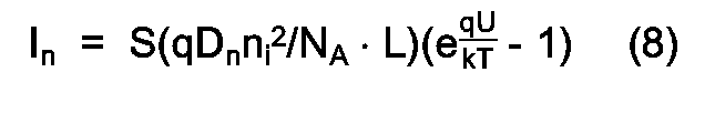
low concentration region 25c of the source, WN is the width of thelow concentration region 25c of the source, Dn is the diffusion coefficient of electron, nA is the accepter concentration in thechannel region 27, L is the length of thechannel region 27, and V is the potential difference between the source and the channel. - ID may be given from the above equations (5) to (8):

- It will be understood from the above equation that as the concentration ND and the width WN of the
low concentration region 25c of the source region are made smaller, the drain current ID becomes smaller and accordingly the breakdown voltage between the source and the drain is increased. - Also in this embodiment, similarly to Fig. 19, the source region and the drain region may be symmetrically provided without damaging the aforementioned variety of advantages of the element utilizing the SOI substrate.
- Fig. 25 shows the twentieth embodiment having a symmetric structure on the source region side and the drain region side. This structure is provided by forming n-
type source region 25 and drainregion 26 havinghigh concentration regions low concentration regions thin film 23 and otherlow concentration regions high concentration regions channel region 27. Further,metal layers low concentration regions high concentration regions channel region 27. In this structure, the metal layers 83A, 83B are ohmically contacted with correspondinghigh concentration regions low concentration regions - A
gate electrode 30 is made, for example, of phosphor-doped polycrystalline silicon. The thickness d of the siliconthin film 23 is selected to be 150 nm, the impurity concentration of the p-channel region 27 approximately 1017 cm-3, the impurity concentration of thehigh concentration regions low concentration regions low concentration regions - Since the source and drain can be symmetrically formed as described above, the element of the present embodiment can be used as a switching element such as an access transistor for a static RAM cell.
- Figs. 26A through 26F show the twenty-first embodiment of the present invention which will be described with a manufacturing process thereof.
- As shown in Fig. 26A, in this embodiment, a
gate insulating film 29 made of Si02 or the like and agate electrode 30 made of polycrystalline silicon are formed in a siliconthin film 23 comprised in anSOI substrate 24. Then, LDD-structured n-type source region 25 and drainregion 26 havinglow concentration regions high concentration regions source region 25 and thedrain region 26 provide shallow junctions. Further, on the surfaces of thehigh concentration regions gate electrode 30, there are formed a silicide layers made of high melting point metal, for example, titanium silicide (TiSi2)layer 100. - Next, as shown in Fig. 26B, an inter-layer
insulating film 101 is formed and awindow 102 for exposing a gate contact portion is formed. Then, as shown in Fig. 26C,windows mask 103. Further,grooves windows film 23. - Next, as shown in Fig. 26D, an n-
type impurity 108 of a low concentration is ion-implanted with a predetermined implanting angle to form n-typelow concentration regions high concentration regions low concentration regions - Next, as shown in Fig. 26E, a
film 109 made, for example, of Ti, which is a high melting point metal, is deposited on the inner surfaces of thegrooves films 110 on the inner walls of thegrooves high concentration regions low concentration regions source region 25 and thedrain region 26. Thetitanium silicide films 110 are ohmically contacted with thehigh concentration regions low concentration regions - Thereafter, as shown in Fig. 26F,
AI films 112 are formed in therespective grooves gate electrode 30 through barrier metal, forexam- ple,TiON films 111, and then asource electrode 31, adrain electrode 32 and a gate lead-outelectrode 113 are formed by the patterning-process, to thereby obtain atarget MISFET 114. In this structure, metal layers83Aand 83B are composed of the titaniumsi icide films 110, thebarrier metal films 111 and theAI films 112. - According to the thus constructed
MISFET 114, it is possible to provide the n-typelow concentration regions metal layer 83A is increased. Simultaneously, by virtue of the Schottky junction formed between the metal layer 83Aand thelow concentration region 25c, a drift current based on an electric field prevailing at the Schottky junction is generated in addition to a diffusion current, whereby the hole current lp is further increased. It is therefore possible to further improve the breakdown voltage between the source and the drain as compared with the foregoing respective embodiments. - Also, in the manufacturing process, it is possible to form the
low concentration region 25c in a remarkably narrow width. Further, the element of the present embodiment can be readily manufactured only by adding a process for forming thegrooves - Figs. 27A through 27E show the twenty-second embodiment which is a modified example of Figs. 26A through 26F. As shown in Fig. 27A, in this embodiment, in a silicon
thin film 23 comprised in anSOI substrate 24 there are formed agate insulating film 29, agate electrode 30 made of polycrystalline silicon, n-type source region 25 and drainregion 26 respectively composed ofhigh concentration regions low concentration regions titanium silicide film 100 is formed over the whole surfaces of thesource region 25, thedrain region 26 and thegate electrode 30. - Next, as shown in Fig. 27B, an inter-larger
insulating film 101 is formed and at the same time,windows insulating film 101 faces, respectively are formed. - Next, as shown in Fig. 27C, n-
type impurities 108 of a low concentration is ion-implanted with a predetermined implanting angle through an ion implanting mask, for example, a photo-resistmask 103 andwindows low concentration regions high concentration regions low concentration regions windows - As shown in Fig. 27D, the surfaces exposing through the
windows film 109 made of a high melting point metal, for example, Ti, and annealed to exert a reaction between titanium and silicon to a depth reaching the Si02 film 22 on the bottom to form titanium silicide (TiSi2)films 110 adjacent to thehigh concentration regions low concentration regions - Next, as shown in Fig. 27E, after removing the
Ti film 109 which has not been reacted and the photo- resistmask 103, aTiON film 111 serving as a barrier metal and anAI film 112 are formed and patterned to form asource electrode 31, adrain electrode 32 and a gate lead-outelectrode 113, thereby obtaining atarget MISFET 115. - Also in the thus constructed
MISFET 115, thelow concentration region 25c is formed to be sufficiently narrower than the diffusion length Lp of the minority carrier (WN « Lp), and a Schottky junction is formed by thetitanium silicide film 110, thereby making it possible to improve the drain breakdown voltage similarly to Figs. 26A through 26F.ln addition, the embodiment of Figs. 27Athrough 27E can form thewindows window 102 for the gate contact and need not form thegrooves - Fig. 28 shows the twenty-third embodiment. As shown in Fig. 28, in a silicon
thin film 23 of, for example, p-type comprised in anSOI substrate 24, there are formed an n-type source region 25 of a high concentration and adrain region 26 having ahigh concentration region 26a within alow concentration region 26c to face the surface. Further, ametal layer 83 is formed adjacent to the outside of thelow concentration region 26c of thedrain region 26 but separated from thechannel region 27. A Schottky junction is formed between themetal layer 83 and thelow concentration region 26c. The distance WN of thedrain region 26c between themetal layer 83 and thechannel region 27 is selected to be shorter than the diffusion length Lp of the positive hole or the minority carrier. Then, agate electrode 30 made, for example, of polycrystalline silicon is formed on thechannel region 27 between thesource region 25 and thedrain region 26 through agate insulating film 29 made of Si02 or the like, while asource electrode 31 and adrain electrode 32 are formed on thesource region 25 and thedrain region 26, respectively, to form aMISFET 116. In this structure, it is necessary to provide themetal layer 83 with a potential identical to the potential of the source or potential of its vicinity. That is, the potential of themetal layer 83 should be lower than that of the channel region. - According to the thus constructed
MISFET 116, themetal layer 83 for forming a Schottky junction with thedrain region 26 is provided on the side of thedrain region 26 close to the source of electron-positive hole couplings generated by the impact ionization, whereby the positive holes generated by the impact ionization can be removed through thedrain region 26 and themetal layer 83 by an action similar to described above to improve the breakdown voltage between the source and the drain.
Claims (21)
Applications Claiming Priority (4)
| Application Number | Priority Date | Filing Date | Title |
|---|---|---|---|
| JP18089990A JP2969833B2 (en) | 1990-07-09 | 1990-07-09 | MIS type semiconductor device |
| JP180898/90 | 1990-07-09 | ||
| JP180899/90 | 1990-07-09 | ||
| JP18089890A JP2969832B2 (en) | 1990-07-09 | 1990-07-09 | MIS type semiconductor device |
Publications (2)
| Publication Number | Publication Date |
|---|---|
| EP0465961A1 EP0465961A1 (en) | 1992-01-15 |
| EP0465961B1 true EP0465961B1 (en) | 1995-08-09 |
Family
ID=26500262
Family Applications (1)
| Application Number | Title | Priority Date | Filing Date |
|---|---|---|---|
| EP91110795A Expired - Lifetime EP0465961B1 (en) | 1990-07-09 | 1991-06-28 | Semiconductor device on a dielectric isolated substrate |
Country Status (4)
| Country | Link |
|---|---|
| US (1) | US5243213A (en) |
| EP (1) | EP0465961B1 (en) |
| KR (1) | KR100289420B1 (en) |
| DE (1) | DE69111929T2 (en) |
Cited By (43)
| Publication number | Priority date | Publication date | Assignee | Title |
|---|---|---|---|---|
| US7683430B2 (en) | 2005-12-19 | 2010-03-23 | Innovative Silicon Isi Sa | Electrically floating body memory cell and array, and method of operating or controlling same |
| US7732816B2 (en) | 2001-06-18 | 2010-06-08 | Innovative Silicon Isi Sa | Semiconductor device |
| US7733693B2 (en) | 2003-05-13 | 2010-06-08 | Innovative Silicon Isi Sa | Semiconductor memory device and method of operating same |
| US7736959B2 (en) | 2003-07-22 | 2010-06-15 | Innovative Silicon Isi Sa | Integrated circuit device, and method of fabricating same |
| US7924630B2 (en) | 2008-10-15 | 2011-04-12 | Micron Technology, Inc. | Techniques for simultaneously driving a plurality of source lines |
| US7933142B2 (en) | 2006-05-02 | 2011-04-26 | Micron Technology, Inc. | Semiconductor memory cell and array using punch-through to program and read same |
| US7933140B2 (en) | 2008-10-02 | 2011-04-26 | Micron Technology, Inc. | Techniques for reducing a voltage swing |
| US7940559B2 (en) | 2006-04-07 | 2011-05-10 | Micron Technology, Inc. | Memory array having a programmable word length, and method of operating same |
| US7947543B2 (en) | 2008-09-25 | 2011-05-24 | Micron Technology, Inc. | Recessed gate silicon-on-insulator floating body device with self-aligned lateral isolation |
| US7957206B2 (en) | 2008-04-04 | 2011-06-07 | Micron Technology, Inc. | Read circuitry for an integrated circuit having memory cells and/or a memory cell array, and method of operating same |
| US7969779B2 (en) | 2006-07-11 | 2011-06-28 | Micron Technology, Inc. | Integrated circuit including memory array having a segmented bit line architecture and method of controlling and/or operating same |
| US8014195B2 (en) | 2008-02-06 | 2011-09-06 | Micron Technology, Inc. | Single transistor memory cell |
| US8064274B2 (en) | 2007-05-30 | 2011-11-22 | Micron Technology, Inc. | Integrated circuit having voltage generation circuitry for memory cell array, and method of operating and/or controlling same |
| US8069377B2 (en) | 2006-06-26 | 2011-11-29 | Micron Technology, Inc. | Integrated circuit having memory array including ECC and column redundancy and method of operating the same |
| US8085594B2 (en) | 2007-06-01 | 2011-12-27 | Micron Technology, Inc. | Reading technique for memory cell with electrically floating body transistor |
| US8139418B2 (en) | 2009-04-27 | 2012-03-20 | Micron Technology, Inc. | Techniques for controlling a direct injection semiconductor memory device |
| US8174881B2 (en) | 2009-11-24 | 2012-05-08 | Micron Technology, Inc. | Techniques for reducing disturbance in a semiconductor device |
| US8189376B2 (en) | 2008-02-08 | 2012-05-29 | Micron Technology, Inc. | Integrated circuit having memory cells including gate material having high work function, and method of manufacturing same |
| US8194487B2 (en) | 2007-09-17 | 2012-06-05 | Micron Technology, Inc. | Refreshing data of memory cells with electrically floating body transistors |
| US8199595B2 (en) | 2009-09-04 | 2012-06-12 | Micron Technology, Inc. | Techniques for sensing a semiconductor memory device |
| US8213226B2 (en) | 2008-12-05 | 2012-07-03 | Micron Technology, Inc. | Vertical transistor memory cell and array |
| US8223574B2 (en) | 2008-11-05 | 2012-07-17 | Micron Technology, Inc. | Techniques for block refreshing a semiconductor memory device |
| US8264041B2 (en) | 2007-01-26 | 2012-09-11 | Micron Technology, Inc. | Semiconductor device with electrically floating body |
| US8310893B2 (en) | 2009-12-16 | 2012-11-13 | Micron Technology, Inc. | Techniques for reducing impact of array disturbs in a semiconductor memory device |
| US8315099B2 (en) | 2009-07-27 | 2012-11-20 | Micron Technology, Inc. | Techniques for providing a direct injection semiconductor memory device |
| US8319294B2 (en) | 2009-02-18 | 2012-11-27 | Micron Technology, Inc. | Techniques for providing a source line plane |
| US8349662B2 (en) | 2007-12-11 | 2013-01-08 | Micron Technology, Inc. | Integrated circuit having memory cell array, and method of manufacturing same |
| US8369177B2 (en) | 2010-03-05 | 2013-02-05 | Micron Technology, Inc. | Techniques for reading from and/or writing to a semiconductor memory device |
| US8411513B2 (en) | 2010-03-04 | 2013-04-02 | Micron Technology, Inc. | Techniques for providing a semiconductor memory device having hierarchical bit lines |
| US8411524B2 (en) | 2010-05-06 | 2013-04-02 | Micron Technology, Inc. | Techniques for refreshing a semiconductor memory device |
| US8416636B2 (en) | 2010-02-12 | 2013-04-09 | Micron Technology, Inc. | Techniques for controlling a semiconductor memory device |
| US8498157B2 (en) | 2009-05-22 | 2013-07-30 | Micron Technology, Inc. | Techniques for providing a direct injection semiconductor memory device |
| US8508994B2 (en) | 2009-04-30 | 2013-08-13 | Micron Technology, Inc. | Semiconductor device with floating gate and electrically floating body |
| US8518774B2 (en) | 2007-03-29 | 2013-08-27 | Micron Technology, Inc. | Manufacturing process for zero-capacitor random access memory circuits |
| US8531878B2 (en) | 2011-05-17 | 2013-09-10 | Micron Technology, Inc. | Techniques for providing a semiconductor memory device |
| US8536628B2 (en) | 2007-11-29 | 2013-09-17 | Micron Technology, Inc. | Integrated circuit having memory cell array including barriers, and method of manufacturing same |
| US8537610B2 (en) | 2009-07-10 | 2013-09-17 | Micron Technology, Inc. | Techniques for providing a semiconductor memory device |
| US8547738B2 (en) | 2010-03-15 | 2013-10-01 | Micron Technology, Inc. | Techniques for providing a semiconductor memory device |
| US8576631B2 (en) | 2010-03-04 | 2013-11-05 | Micron Technology, Inc. | Techniques for sensing a semiconductor memory device |
| US8710566B2 (en) | 2009-03-04 | 2014-04-29 | Micron Technology, Inc. | Techniques for forming a contact to a buried diffusion layer in a semiconductor memory device |
| US8748959B2 (en) | 2009-03-31 | 2014-06-10 | Micron Technology, Inc. | Semiconductor memory device |
| US8873283B2 (en) | 2005-09-07 | 2014-10-28 | Micron Technology, Inc. | Memory cell and memory cell array having an electrically floating body transistor, and methods of operating same |
| US9559216B2 (en) | 2011-06-06 | 2017-01-31 | Micron Technology, Inc. | Semiconductor memory device and method for biasing same |
Families Citing this family (39)
| Publication number | Priority date | Publication date | Assignee | Title |
|---|---|---|---|---|
| KR0126457B1 (en) * | 1992-01-08 | 1997-12-26 | 기타오카 다카시 | Large scale integrated circuit device and thin film forming method and apparatus for the same |
| EP0571027A1 (en) * | 1992-05-21 | 1993-11-24 | Koninklijke Philips Electronics N.V. | Semiconductor device comprising a lateral DMOST with breakdown voltage raising zones and provisions for exchanging charge with the back gate region |
| US5315144A (en) * | 1992-09-18 | 1994-05-24 | Harris Corporation | Reduction of bipolar gain and improvement in snap-back sustaining voltage in SOI field effect transistor |
| JP3818673B2 (en) * | 1993-03-10 | 2006-09-06 | 株式会社デンソー | Semiconductor device |
| JP3375681B2 (en) * | 1993-06-04 | 2003-02-10 | 株式会社半導体エネルギー研究所 | Method for manufacturing semiconductor device |
| US5719065A (en) | 1993-10-01 | 1998-02-17 | Semiconductor Energy Laboratory Co., Ltd. | Method for manufacturing semiconductor device with removable spacers |
| US6906383B1 (en) * | 1994-07-14 | 2005-06-14 | Semiconductor Energy Laboratory Co., Ltd. | Semiconductor device and method of manufacture thereof |
| EP0735592A3 (en) * | 1995-03-31 | 1997-11-05 | Nippon Telegraph And Telephone Corporation | MOS thin film transistor and method of fabricating the same |
| US5532175A (en) * | 1995-04-17 | 1996-07-02 | Motorola, Inc. | Method of adjusting a threshold voltage for a semiconductor device fabricated on a semiconductor on insulator substrate |
| JP2770784B2 (en) * | 1995-05-31 | 1998-07-02 | 日本電気株式会社 | Silicon-on-insulator semiconductor device |
| US5681761A (en) * | 1995-12-28 | 1997-10-28 | Philips Electronics North America Corporation | Microwave power SOI-MOSFET with high conductivity metal gate |
| TW374196B (en) * | 1996-02-23 | 1999-11-11 | Semiconductor Energy Lab Co Ltd | Semiconductor thin film and method for manufacturing the same and semiconductor device and method for manufacturing the same |
| WO1998027597A1 (en) * | 1996-12-19 | 1998-06-25 | Honeywell Inc. | Mos device having a body to source contact feature for use on soi substrates |
| US6686623B2 (en) | 1997-11-18 | 2004-02-03 | Semiconductor Energy Laboratory Co., Ltd. | Nonvolatile memory and electronic apparatus |
| US6111293A (en) * | 1998-02-16 | 2000-08-29 | United Silicon Incorporated | Silicon-on-insulator MOS structure |
| US6300661B1 (en) * | 1998-04-14 | 2001-10-09 | Advanced Micro Devices, Inc. | Mutual implant region used for applying power/ground to a source of a transistor and a well of a substrate |
| JP2000012864A (en) | 1998-06-22 | 2000-01-14 | Semiconductor Energy Lab Co Ltd | Manufacture of semiconductor device |
| US6271101B1 (en) * | 1998-07-29 | 2001-08-07 | Semiconductor Energy Laboratory Co., Ltd. | Process for production of SOI substrate and process for production of semiconductor device |
| US6559036B1 (en) * | 1998-08-07 | 2003-05-06 | Semiconductor Energy Laboratory Co., Ltd. | Semiconductor device and method of manufacturing the same |
| JP4476390B2 (en) | 1998-09-04 | 2010-06-09 | 株式会社半導体エネルギー研究所 | Method for manufacturing semiconductor device |
| GB2344689A (en) | 1998-12-07 | 2000-06-14 | Ericsson Telefon Ab L M | Analogue switch |
| GB9915235D0 (en) * | 1999-06-30 | 1999-09-01 | Crosfield Joseph & Sons | Liquid treatment agents |
| JP3845272B2 (en) * | 2001-06-19 | 2006-11-15 | シャープ株式会社 | SRAM and manufacturing method thereof |
| KR100425462B1 (en) * | 2001-09-10 | 2004-03-30 | 삼성전자주식회사 | Semiconductor device on SOI(silicon on insulator) structure) and method for manufacturing the same |
| KR20020062887A (en) * | 2002-06-29 | 2002-07-31 | 김진수 | A Common Salt Composition for Containing Garlic Ingredients and Manufacture Method thereof |
| US7112856B2 (en) * | 2002-07-12 | 2006-09-26 | Samsung Electronics Co., Ltd. | Semiconductor device having a merged region and method of fabrication |
| US7084423B2 (en) | 2002-08-12 | 2006-08-01 | Acorn Technologies, Inc. | Method for depinning the Fermi level of a semiconductor at an electrical junction and devices incorporating such junctions |
| US6833556B2 (en) * | 2002-08-12 | 2004-12-21 | Acorn Technologies, Inc. | Insulated gate field effect transistor having passivated schottky barriers to the channel |
| US20040222485A1 (en) * | 2002-12-17 | 2004-11-11 | Haynie Sheldon D. | Bladed silicon-on-insulator semiconductor devices and method of making |
| KR100542986B1 (en) | 2003-04-29 | 2006-01-20 | 삼성에스디아이 주식회사 | TFT, Method for fabricating the TFT and Flat panel device using the same |
| GB0316395D0 (en) * | 2003-07-12 | 2003-08-13 | Hewlett Packard Development Co | A transistor device with metallic electrodes and a method for use in forming such a device |
| KR100513249B1 (en) * | 2003-09-05 | 2005-09-07 | (주)에스에스디21씨 | Manufacturing method of salt containing garlic ingredient |
| US7109532B1 (en) * | 2003-12-23 | 2006-09-19 | Lee Zachary K | High Ion/Ioff SOI MOSFET using body voltage control |
| KR100878284B1 (en) | 2007-03-09 | 2009-01-12 | 삼성모바일디스플레이주식회사 | Thin film transistor and fabricating for the same and organic light emitting diode device display comprising the same |
| US8773933B2 (en) | 2012-03-16 | 2014-07-08 | Micron Technology, Inc. | Techniques for accessing memory cells |
| KR101064402B1 (en) * | 2009-01-12 | 2011-09-14 | 삼성모바일디스플레이주식회사 | Thin film transistor, method of manufacturing the thin film transistor and flat panel display device having the thin film transistor |
| US9966141B2 (en) * | 2016-02-19 | 2018-05-08 | Nscore, Inc. | Nonvolatile memory cell employing hot carrier effect for data storage |
| US9620611B1 (en) | 2016-06-17 | 2017-04-11 | Acorn Technology, Inc. | MIS contact structure with metal oxide conductor |
| US10170627B2 (en) | 2016-11-18 | 2019-01-01 | Acorn Technologies, Inc. | Nanowire transistor with source and drain induced by electrical contacts with negative schottky barrier height |
Family Cites Families (4)
| Publication number | Priority date | Publication date | Assignee | Title |
|---|---|---|---|---|
| JPS55113359A (en) * | 1979-02-22 | 1980-09-01 | Fujitsu Ltd | Semiconductor integrated circuit device |
| EP0144654A3 (en) * | 1983-11-03 | 1987-10-07 | General Electric Company | Semiconductor device structure including a dielectrically-isolated insulated-gate transistor |
| US4879585A (en) * | 1984-03-31 | 1989-11-07 | Kabushiki Kaisha Toshiba | Semiconductor device |
| JP2510710B2 (en) * | 1988-12-13 | 1996-06-26 | 三菱電機株式会社 | MOS field effect transistor formed in semiconductor layer on insulator substrate |
-
1991
- 1991-06-28 EP EP91110795A patent/EP0465961B1/en not_active Expired - Lifetime
- 1991-06-28 DE DE69111929T patent/DE69111929T2/en not_active Expired - Fee Related
- 1991-07-08 KR KR1019910011477A patent/KR100289420B1/en not_active IP Right Cessation
- 1991-07-08 US US07/726,904 patent/US5243213A/en not_active Expired - Fee Related
Cited By (59)
| Publication number | Priority date | Publication date | Assignee | Title |
|---|---|---|---|---|
| US7732816B2 (en) | 2001-06-18 | 2010-06-08 | Innovative Silicon Isi Sa | Semiconductor device |
| US7733693B2 (en) | 2003-05-13 | 2010-06-08 | Innovative Silicon Isi Sa | Semiconductor memory device and method of operating same |
| US7736959B2 (en) | 2003-07-22 | 2010-06-15 | Innovative Silicon Isi Sa | Integrated circuit device, and method of fabricating same |
| US8873283B2 (en) | 2005-09-07 | 2014-10-28 | Micron Technology, Inc. | Memory cell and memory cell array having an electrically floating body transistor, and methods of operating same |
| US7683430B2 (en) | 2005-12-19 | 2010-03-23 | Innovative Silicon Isi Sa | Electrically floating body memory cell and array, and method of operating or controlling same |
| US7940559B2 (en) | 2006-04-07 | 2011-05-10 | Micron Technology, Inc. | Memory array having a programmable word length, and method of operating same |
| US8134867B2 (en) | 2006-04-07 | 2012-03-13 | Micron Technology, Inc. | Memory array having a programmable word length, and method of operating same |
| US7933142B2 (en) | 2006-05-02 | 2011-04-26 | Micron Technology, Inc. | Semiconductor memory cell and array using punch-through to program and read same |
| US8295078B2 (en) | 2006-05-02 | 2012-10-23 | Micron Technology, Inc. | Semiconductor memory cell and array using punch-through to program and read same |
| US8069377B2 (en) | 2006-06-26 | 2011-11-29 | Micron Technology, Inc. | Integrated circuit having memory array including ECC and column redundancy and method of operating the same |
| US8402326B2 (en) | 2006-06-26 | 2013-03-19 | Micron Technology, Inc. | Integrated circuit having memory array including ECC and column redundancy and method of operating same |
| US8395937B2 (en) | 2006-07-11 | 2013-03-12 | Micron Technology, Inc. | Integrated circuit including memory array having a segmented bit line architecture and method of controlling and/or operating same |
| US7969779B2 (en) | 2006-07-11 | 2011-06-28 | Micron Technology, Inc. | Integrated circuit including memory array having a segmented bit line architecture and method of controlling and/or operating same |
| US8264041B2 (en) | 2007-01-26 | 2012-09-11 | Micron Technology, Inc. | Semiconductor device with electrically floating body |
| US8518774B2 (en) | 2007-03-29 | 2013-08-27 | Micron Technology, Inc. | Manufacturing process for zero-capacitor random access memory circuits |
| US8064274B2 (en) | 2007-05-30 | 2011-11-22 | Micron Technology, Inc. | Integrated circuit having voltage generation circuitry for memory cell array, and method of operating and/or controlling same |
| US8085594B2 (en) | 2007-06-01 | 2011-12-27 | Micron Technology, Inc. | Reading technique for memory cell with electrically floating body transistor |
| US8659948B2 (en) | 2007-06-01 | 2014-02-25 | Micron Technology, Inc. | Techniques for reading a memory cell with electrically floating body transistor |
| US8446794B2 (en) | 2007-09-17 | 2013-05-21 | Micron Technology, Inc. | Refreshing data of memory cells with electrically floating body transistors |
| US8194487B2 (en) | 2007-09-17 | 2012-06-05 | Micron Technology, Inc. | Refreshing data of memory cells with electrically floating body transistors |
| US8536628B2 (en) | 2007-11-29 | 2013-09-17 | Micron Technology, Inc. | Integrated circuit having memory cell array including barriers, and method of manufacturing same |
| US8349662B2 (en) | 2007-12-11 | 2013-01-08 | Micron Technology, Inc. | Integrated circuit having memory cell array, and method of manufacturing same |
| US8014195B2 (en) | 2008-02-06 | 2011-09-06 | Micron Technology, Inc. | Single transistor memory cell |
| US8325515B2 (en) | 2008-02-06 | 2012-12-04 | Micron Technology, Inc. | Integrated circuit device |
| US8189376B2 (en) | 2008-02-08 | 2012-05-29 | Micron Technology, Inc. | Integrated circuit having memory cells including gate material having high work function, and method of manufacturing same |
| US8274849B2 (en) | 2008-04-04 | 2012-09-25 | Micron Technology, Inc. | Read circuitry for an integrated circuit having memory cells and/or a memory cell array, and method of operating same |
| US7957206B2 (en) | 2008-04-04 | 2011-06-07 | Micron Technology, Inc. | Read circuitry for an integrated circuit having memory cells and/or a memory cell array, and method of operating same |
| US8790968B2 (en) | 2008-09-25 | 2014-07-29 | Micron Technology, Inc. | Recessed gate silicon-on-insulator floating body device with self-aligned lateral isolation |
| US7947543B2 (en) | 2008-09-25 | 2011-05-24 | Micron Technology, Inc. | Recessed gate silicon-on-insulator floating body device with self-aligned lateral isolation |
| US8315083B2 (en) | 2008-10-02 | 2012-11-20 | Micron Technology Inc. | Techniques for reducing a voltage swing |
| US7933140B2 (en) | 2008-10-02 | 2011-04-26 | Micron Technology, Inc. | Techniques for reducing a voltage swing |
| US7924630B2 (en) | 2008-10-15 | 2011-04-12 | Micron Technology, Inc. | Techniques for simultaneously driving a plurality of source lines |
| US8223574B2 (en) | 2008-11-05 | 2012-07-17 | Micron Technology, Inc. | Techniques for block refreshing a semiconductor memory device |
| US8213226B2 (en) | 2008-12-05 | 2012-07-03 | Micron Technology, Inc. | Vertical transistor memory cell and array |
| US8319294B2 (en) | 2009-02-18 | 2012-11-27 | Micron Technology, Inc. | Techniques for providing a source line plane |
| US8710566B2 (en) | 2009-03-04 | 2014-04-29 | Micron Technology, Inc. | Techniques for forming a contact to a buried diffusion layer in a semiconductor memory device |
| US8748959B2 (en) | 2009-03-31 | 2014-06-10 | Micron Technology, Inc. | Semiconductor memory device |
| US8508970B2 (en) | 2009-04-27 | 2013-08-13 | Micron Technology, Inc. | Techniques for providing a direct injection semiconductor memory device |
| US8400811B2 (en) | 2009-04-27 | 2013-03-19 | Micron Technology, Inc. | Techniques for providing a direct injection semiconductor memory device having ganged carrier injection lines |
| US8139418B2 (en) | 2009-04-27 | 2012-03-20 | Micron Technology, Inc. | Techniques for controlling a direct injection semiconductor memory device |
| US8351266B2 (en) | 2009-04-27 | 2013-01-08 | Micron Technology, Inc. | Techniques for controlling a direct injection semiconductor memory device |
| US8508994B2 (en) | 2009-04-30 | 2013-08-13 | Micron Technology, Inc. | Semiconductor device with floating gate and electrically floating body |
| US8498157B2 (en) | 2009-05-22 | 2013-07-30 | Micron Technology, Inc. | Techniques for providing a direct injection semiconductor memory device |
| US8537610B2 (en) | 2009-07-10 | 2013-09-17 | Micron Technology, Inc. | Techniques for providing a semiconductor memory device |
| US8587996B2 (en) | 2009-07-27 | 2013-11-19 | Micron Technology, Inc. | Techniques for providing a direct injection semiconductor memory device |
| US8315099B2 (en) | 2009-07-27 | 2012-11-20 | Micron Technology, Inc. | Techniques for providing a direct injection semiconductor memory device |
| US9076543B2 (en) | 2009-07-27 | 2015-07-07 | Micron Technology, Inc. | Techniques for providing a direct injection semiconductor memory device |
| US8199595B2 (en) | 2009-09-04 | 2012-06-12 | Micron Technology, Inc. | Techniques for sensing a semiconductor memory device |
| US8174881B2 (en) | 2009-11-24 | 2012-05-08 | Micron Technology, Inc. | Techniques for reducing disturbance in a semiconductor device |
| US8310893B2 (en) | 2009-12-16 | 2012-11-13 | Micron Technology, Inc. | Techniques for reducing impact of array disturbs in a semiconductor memory device |
| US8416636B2 (en) | 2010-02-12 | 2013-04-09 | Micron Technology, Inc. | Techniques for controlling a semiconductor memory device |
| US8576631B2 (en) | 2010-03-04 | 2013-11-05 | Micron Technology, Inc. | Techniques for sensing a semiconductor memory device |
| US8411513B2 (en) | 2010-03-04 | 2013-04-02 | Micron Technology, Inc. | Techniques for providing a semiconductor memory device having hierarchical bit lines |
| US8369177B2 (en) | 2010-03-05 | 2013-02-05 | Micron Technology, Inc. | Techniques for reading from and/or writing to a semiconductor memory device |
| US8547738B2 (en) | 2010-03-15 | 2013-10-01 | Micron Technology, Inc. | Techniques for providing a semiconductor memory device |
| US8630126B2 (en) | 2010-05-06 | 2014-01-14 | Micron Technology, Inc. | Techniques for refreshing a semiconductor memory device |
| US8411524B2 (en) | 2010-05-06 | 2013-04-02 | Micron Technology, Inc. | Techniques for refreshing a semiconductor memory device |
| US8531878B2 (en) | 2011-05-17 | 2013-09-10 | Micron Technology, Inc. | Techniques for providing a semiconductor memory device |
| US9559216B2 (en) | 2011-06-06 | 2017-01-31 | Micron Technology, Inc. | Semiconductor memory device and method for biasing same |
Also Published As
| Publication number | Publication date |
|---|---|
| US5243213A (en) | 1993-09-07 |
| KR100289420B1 (en) | 2001-06-01 |
| EP0465961A1 (en) | 1992-01-15 |
| KR920003549A (en) | 1992-02-29 |
| DE69111929T2 (en) | 1996-03-28 |
| DE69111929D1 (en) | 1995-09-14 |
Similar Documents
| Publication | Publication Date | Title |
|---|---|---|
| EP0465961B1 (en) | Semiconductor device on a dielectric isolated substrate | |
| JP3462301B2 (en) | Semiconductor device and manufacturing method thereof | |
| US6121666A (en) | Split gate oxide asymmetric MOS devices | |
| US6268630B1 (en) | Silicon-on-insulator field effect transistor with improved body ties for rad-hard applications | |
| US5266515A (en) | Fabricating dual gate thin film transistors | |
| US4935379A (en) | Semiconductor device and method of manufacturing the same | |
| US6110783A (en) | Method for forming a notched gate oxide asymmetric MOS device | |
| US4052229A (en) | Process for preparing a substrate for mos devices of different thresholds | |
| US6163053A (en) | Semiconductor device having opposite-polarity region under channel | |
| US5674760A (en) | Method of forming isolation regions in a MOS transistor device | |
| US6774454B2 (en) | Semiconductor device with an silicon insulator (SOI) substrate | |
| US5512497A (en) | Method of manufacturing a semiconductor integrated circuit device | |
| EP0596468A2 (en) | MOSFET of LDD type and a method for fabricating the same | |
| KR19980064498A (en) | Semiconductor device and manufacturing method thereof | |
| US4922315A (en) | Control gate lateral silicon-on-insulator bipolar transistor | |
| US6091111A (en) | High voltage mos device having an extended drain region with different dopant species | |
| JP2700955B2 (en) | Semiconductor device with field effect transistor | |
| US4939154A (en) | Method of fabricating an insulated gate semiconductor device having a self-aligned gate | |
| JP3103159B2 (en) | Semiconductor device | |
| KR0180310B1 (en) | Method for manufacturing cmos transistor | |
| US11508806B1 (en) | Low leakage ESD MOSFET | |
| US5688701A (en) | Method of making semiconductor device having a plurality of impurity layers | |
| US5242849A (en) | Method for the fabrication of MOS devices | |
| US5057894A (en) | Semiconductor integrated circuit device | |
| US5338958A (en) | Semicondcutor device with high speed field effect transistor structure reducing concentrations of electric field near drain region |
Legal Events
| Date | Code | Title | Description |
|---|---|---|---|
| PUAI | Public reference made under article 153(3) epc to a published international application that has entered the european phase |
Free format text: ORIGINAL CODE: 0009012 |
|
| AK | Designated contracting states |
Kind code of ref document: A1 Designated state(s): DE FR GB |
|
| 17P | Request for examination filed |
Effective date: 19920604 |
|
| 17Q | First examination report despatched |
Effective date: 19940314 |
|
| GRAA | (expected) grant |
Free format text: ORIGINAL CODE: 0009210 |
|
| AK | Designated contracting states |
Kind code of ref document: B1 Designated state(s): DE FR GB |
|
| REF | Corresponds to: |
Ref document number: 69111929 Country of ref document: DE Date of ref document: 19950914 |
|
| ET | Fr: translation filed | ||
| PLBE | No opposition filed within time limit |
Free format text: ORIGINAL CODE: 0009261 |
|
| STAA | Information on the status of an ep patent application or granted ep patent |
Free format text: STATUS: NO OPPOSITION FILED WITHIN TIME LIMIT |
|
| 26N | No opposition filed | ||
| PGFP | Annual fee paid to national office [announced via postgrant information from national office to epo] |
Ref country code: FR Payment date: 20010611 Year of fee payment: 11 |
|
| PGFP | Annual fee paid to national office [announced via postgrant information from national office to epo] |
Ref country code: DE Payment date: 20010618 Year of fee payment: 11 |
|
| PGFP | Annual fee paid to national office [announced via postgrant information from national office to epo] |
Ref country code: GB Payment date: 20010627 Year of fee payment: 11 |
|
| REG | Reference to a national code |
Ref country code: GB Ref legal event code: IF02 |
|
| PG25 | Lapsed in a contracting state [announced via postgrant information from national office to epo] |
Ref country code: GB Free format text: LAPSE BECAUSE OF NON-PAYMENT OF DUE FEES Effective date: 20020628 |
|
| PG25 | Lapsed in a contracting state [announced via postgrant information from national office to epo] |
Ref country code: DE Free format text: LAPSE BECAUSE OF NON-PAYMENT OF DUE FEES Effective date: 20030101 |
|
| GBPC | Gb: european patent ceased through non-payment of renewal fee |
Effective date: 20020628 |
|
| PG25 | Lapsed in a contracting state [announced via postgrant information from national office to epo] |
Ref country code: FR Free format text: LAPSE BECAUSE OF NON-PAYMENT OF DUE FEES Effective date: 20030228 |
|
| REG | Reference to a national code |
Ref country code: FR Ref legal event code: ST |