EP0468135A2 - A high speed dynamic, random access memory with extended reset/precharge time - Google Patents
A high speed dynamic, random access memory with extended reset/precharge time Download PDFInfo
- Publication number
- EP0468135A2 EP0468135A2 EP91104396A EP91104396A EP0468135A2 EP 0468135 A2 EP0468135 A2 EP 0468135A2 EP 91104396 A EP91104396 A EP 91104396A EP 91104396 A EP91104396 A EP 91104396A EP 0468135 A2 EP0468135 A2 EP 0468135A2
- Authority
- EP
- European Patent Office
- Prior art keywords
- row address
- dram
- level
- circuit
- active
- Prior art date
- Legal status (The legal status is an assumption and is not a legal conclusion. Google has not performed a legal analysis and makes no representation as to the accuracy of the status listed.)
- Granted
Links
Images


Classifications
-
- G—PHYSICS
- G11—INFORMATION STORAGE
- G11C—STATIC STORES
- G11C11/00—Digital stores characterised by the use of particular electric or magnetic storage elements; Storage elements therefor
- G11C11/21—Digital stores characterised by the use of particular electric or magnetic storage elements; Storage elements therefor using electric elements
- G11C11/34—Digital stores characterised by the use of particular electric or magnetic storage elements; Storage elements therefor using electric elements using semiconductor devices
- G11C11/40—Digital stores characterised by the use of particular electric or magnetic storage elements; Storage elements therefor using electric elements using semiconductor devices using transistors
- G11C11/401—Digital stores characterised by the use of particular electric or magnetic storage elements; Storage elements therefor using electric elements using semiconductor devices using transistors forming cells needing refreshing or charge regeneration, i.e. dynamic cells
- G11C11/4063—Auxiliary circuits, e.g. for addressing, decoding, driving, writing, sensing or timing
- G11C11/407—Auxiliary circuits, e.g. for addressing, decoding, driving, writing, sensing or timing for memory cells of the field-effect type
- G11C11/409—Read-write [R-W] circuits
- G11C11/4094—Bit-line management or control circuits
-
- G—PHYSICS
- G11—INFORMATION STORAGE
- G11C—STATIC STORES
- G11C11/00—Digital stores characterised by the use of particular electric or magnetic storage elements; Storage elements therefor
- G11C11/21—Digital stores characterised by the use of particular electric or magnetic storage elements; Storage elements therefor using electric elements
- G11C11/34—Digital stores characterised by the use of particular electric or magnetic storage elements; Storage elements therefor using electric elements using semiconductor devices
- G11C11/40—Digital stores characterised by the use of particular electric or magnetic storage elements; Storage elements therefor using electric elements using semiconductor devices using transistors
- G11C11/401—Digital stores characterised by the use of particular electric or magnetic storage elements; Storage elements therefor using electric elements using semiconductor devices using transistors forming cells needing refreshing or charge regeneration, i.e. dynamic cells
- G11C11/4063—Auxiliary circuits, e.g. for addressing, decoding, driving, writing, sensing or timing
- G11C11/407—Auxiliary circuits, e.g. for addressing, decoding, driving, writing, sensing or timing for memory cells of the field-effect type
- G11C11/4072—Circuits for initialization, powering up or down, clearing memory or presetting
-
- G—PHYSICS
- G11—INFORMATION STORAGE
- G11C—STATIC STORES
- G11C11/00—Digital stores characterised by the use of particular electric or magnetic storage elements; Storage elements therefor
- G11C11/21—Digital stores characterised by the use of particular electric or magnetic storage elements; Storage elements therefor using electric elements
- G11C11/34—Digital stores characterised by the use of particular electric or magnetic storage elements; Storage elements therefor using electric elements using semiconductor devices
- G11C11/40—Digital stores characterised by the use of particular electric or magnetic storage elements; Storage elements therefor using electric elements using semiconductor devices using transistors
- G11C11/401—Digital stores characterised by the use of particular electric or magnetic storage elements; Storage elements therefor using electric elements using semiconductor devices using transistors forming cells needing refreshing or charge regeneration, i.e. dynamic cells
- G11C11/4063—Auxiliary circuits, e.g. for addressing, decoding, driving, writing, sensing or timing
- G11C11/407—Auxiliary circuits, e.g. for addressing, decoding, driving, writing, sensing or timing for memory cells of the field-effect type
- G11C11/4076—Timing circuits
-
- G—PHYSICS
- G11—INFORMATION STORAGE
- G11C—STATIC STORES
- G11C8/00—Arrangements for selecting an address in a digital store
- G11C8/18—Address timing or clocking circuits; Address control signal generation or management, e.g. for row address strobe [RAS] or column address strobe [CAS] signals
Definitions
- This invention relates to dynamic random access semiconductor memories (DRAM) and, more particularly, to a system for increasing the available time for row reset/precharge time in a DRAM.
- DRAM dynamic random access semiconductor memories
- an address system in which row and column addresses are multiplexed through a set of address terminals in response to a pair of external clocks.
- the first clock generates a row address strobe (RAS) and a second clock generates a column address strobe (CAS).
- RAS row address strobe
- CAS column address strobe
- the RAS signal is active for a portion of the time and inactive for another portion of the time. During its active state, it is at a logical low level and during its inactive state, it is at a logical high level. When the RAS signal is in its inactive state, presetting and recharging of the DRAM circuitry is accomplished to ready it for the next memory cycle.
- word lines i.e., X address lines
- the active state low logical level
- the standby state high logical level
- an internal read-write cycle restores charges to memory cell storage capacitors; address buffers and sense amplifiers are reset; and bit lines are precharged.
- DRAMS have seen wide usage in personal computers (PC).
- PC personal computers
- a personal computer's clock is eight or ten mHz
- most DRAMS are fast enough to keep up with the PC's central processing unit (CPU). If the CPU clock runs faster, a conventional DRAM is unable to keep up with the CPU's clock rate and system performance is thereby degraded.
- each clock cycle is, at least, 100 nanoseconds long and there is more than sufficient time to perform the DRAM's reset/precharge functions.
- each CPU clock cycle is 30 nanoseconds and, a computer-generated RAS signal allows only approximately 20 nanoseconds for reset/precharge functions. This is inadequate for high speed DRAMS, which require a reset/precharge time of 30 nanoseconds.
- Sense-amplifiers are connected to the bit line pair.
- Static memory cells are also connected to the bit lines and serve as an auxiliary memory.
- the static memory cells statically hold data voltages stored in an array of memory cells connected to the selected word line until another word line is selected.
- the data voltages can be stored in the static memory cells. Therefore, even during the precharge period, data read/write is enabled.
- Japanese Patent 60-211696 issued October 24, 1985 to Miyazawa, entitled “Dynamic Ram”, relates to a technique for reading a dynamic RAM at a high speed by lowering slightly a precharge level by means of a level adjusting circuit while synchronizing a selection action of a memory cell.
- Japanese Patent 61-230697 issued October 14, 1986 to Miyatake, entitled “Dynamic Semiconductor Memory Device”, relates to a technique to shorten the access time and to attain a high-speed operation of a dynamic semiconductor memory device by lowering the precharging level of an address decoder circuit down to about half of the power supply voltage.
- Japanese Patent 61-222089 issued October 2, 1986 to Watanabe, entitled “Equalizing and Precharging Circuit”, relates to a method and circuit to shorten access time and to stabilize reading operation by using a MOSFET for precharging in time division an active load having high resistance.
- Japanese Patent 61-126683 issued June 14, 1986 to Aono entitled “Semiconductor Memory Device”, discloses a circuit to decrease a delay due to a precharging and to make an action highly speedy by precharging a bit line with plural electric current paths.
- European Patent Application no. 80101777.3 filed April 3, 1980 by Shoji and published October 29, 1980 discloses a memory device operable at high-speed and with low power consumption.
- row address information and column address information are incorporated in synchronism with a row strobe signal and a column strobe signal, respectively, and refresh is effected in response to a row address.
- the device comprises a plurality of groups of selection gates for selectively supplying the incorporated column address information to a part of a plurality of column address decoders.
- a computer system which includes a DRAM having a plurality of memory cells arranged in rows and columns.
- the system includes a row address buffer, and circuitry for generating a row address strobe signal that exhibits both active and inactive levels during each DRAM memory cycle and first and second transitions between those levels.
- a read-in circuit causes read-in of a row address to the DRAM's row address buffer.
- a delay circuit is responsive to a delayed lagging transition of a row address strobe signal to provide an extended duration control signal which delays an output from the row address buffer.
- a reset/precharge circuit is active during both the inactive row address strobe signal and the extended duration control signal to reset and precharge circuits and memory cells in the DRAM.
- a waveform diagram of a prior art DRAM memory cycle is illustrated which employs three CPU clock cycles.
- Such DRAM operations are found in personal computers employing a microchannel configuration (e.g., IBM PS2).
- the RAS signal transitions from a low (active) level to the high (inactive) level and the RAS reset/precharge cycle commences. It is during this time that the resetting and precharging actions occur within the DRAM in preparation for the next read, write, or refresh cycle.
- the address lines transition to enable, at time A, addresses to be read into a DRAM controller register in preparation for read-in to the DRAM.
- the RAS signal transitions to the low level and the addresses in the DRAM controller register are read into a row address buffer on the DRAM chip.
- column addresses are read into a column address register in the DRAM controller.
- the column address strobe CAS
- the addresses are decoded and either read, write, or refresh actions occur.
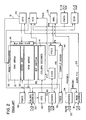
- FIG. 2 a diagram of a prior-art high speed DRAM memory chip is illustrated which implements the waveforms of Fig. 1.
- a pair of 64K arrays of storage cells 10 and 12 are accessed by a column decoder 14 and a wordline (row) driver 16. Row addresses are received into row address buffer 18 and column addresses are received into column address buffer 20.
- a RAS signal, generated by the CPU, is applied via terminal 22 to RASGEN circuit 24 which, in turn, generates two signals. The first is a signal designated PRASBI which tells row address buffer 18 to latch the row (word) address signals. This occurs at time B in Fig. 1. Row address buffer 18 immediately manifests true and complement signals corresponding to the row addresses on line 26.
- RASGEN circuit 24 also generates a signal denoted PRASBII (a signal that initiates a new memory cycle).
- PRASBII a signal that initiates a new memory cycle.
- the PRASBII signal causes a boost wordline clock (BWL) 28 to be triggered.
- BWL boost wordline clock
- an output from BWL 28 is applied to wordline drivers 16 and sample array 34.
- the address true and complement signals on line 26 are decoded in row address decoder (RPD) 30 and applied to word line drivers 16.
- RPD row address decoder
- the output from BWL 28 causes the word lines to be gated to access arrays 12 and 16 in accordance with the decoded address signals and also causes the latching of read-out data in sense amplifiers 32.
- sense amplifiers 32 The latching of sense amplifiers 32 is caused by an output from sample array 34 which, in turn, causes trigger latch clock (PSCG) 36 to transmit an output to sense amp latching clock 38 (PSBCG).
- PSCG trigger latch clock
- PSBCG sense amp latching clock 38
- a reset/precharge circuit 33 is responsive to an output from row address decoder 30, via line 31 to reset/precharge circuit 33 and enables that circuit to reset and precharge the memory circuits within arrays 10 and 12.
- the level on line 31 only provides an activating input to reset/precharge circuits 33 when the address inputs to decoder 30 are inactive. When the address circuits become active, reset precharge circuit 33 is deactivated. Since the circuit of Fig. 2 is in the prior art, its additional detailed operation will not be further described.
- FIG. 4 a DRAM is shown that incorporates the invention.
- RASGEN circuit 24 has been modified to provide a new signal PRASD, and the timing and functions of PRASBI and PRASBII have been changed.
- Row address buffer 18 now latches in row addresses when PRASBI becomes active.
- the outputs from row address buffer 18 (ADRS T/C) are delayed until activation of the PRASD signal on line 42 from RASGEN circuit 24.
- the RAS signal is applied via terminal 22, to transistors Q2 and Q1 and then through transistors Q6 and Q5 to node 3 and an input to NOR circuit 50. So long as a NOR condition is present at the inputs to NOR circuit 50, its output is at an active level. This causes the PRASBI, PRASBII, and PRASD signals to be at the high or inactive state.
- fuse 52 is blown, and causes a signal appearing at node 3 to be applied through delay circuit 54 to an input to NOR circuit 50.
- delay circuit 54 The details of delay circuit 54 are shown expanded at 56 in Fig. 5). Consequently, an active output at node 5 from NOR circuit 50 is present only after the level at node 3 transitions from the high state to the low state (indicating the termination of the RAS reset/precharge state) and that transition is delayed and arrives at NOR circuit 50 via delay 54.
- the PRASD and PRASBII signals derived when node 5 transitions to the active state are activated at the end of the delayed RAS signal.
- the PRASBI signal appearing at node 58 is activated when node 3 goes low and immediately causes the row addresses in row address buffer 18 to be latched.
- fuse 52 is not blown and the circuit operates as the prior art circuit shown in Fig. 2.
- Fig. 6 a schematic diagram of row address buffer circuit 18 is shown.
- the circuit is modification of a prior circuit shown in U.S. Patent 4,697,108 to Chappell et al.
- the modified portion is shown in dotted box 60.
- the address true and complement signals appear at terminals 62 and 64 respectively. They are gated by the PRASD signal appearing on terminal 64 through NAND GATES 67 and 69. As soon as the PRASBI signal on terminal 66 is activated, the circuit latches the addresses appearing on row address input 68. The address true and complement outputs on terminals 62 and 64 do not become active until the PRASD signal on terminal input 64 is asserted.
- the RAS reset/precharge time is extended by an on-chip generated control signal derived from NOR circuit 50 in Fig. 5. That output and its duration is controlled by the fall at node 3 of the RAS signal and its time delay through delay circuit 54.
- the extension by the delay circuit is only a fraction of the RAS reset time, thus enabling more accurate timing of the RAS cycle.
Abstract
Description
- This invention relates to dynamic random access semiconductor memories (DRAM) and, more particularly, to a system for increasing the available time for row reset/precharge time in a DRAM.
- In modern DRAM's, an address system is employed in which row and column addresses are multiplexed through a set of address terminals in response to a pair of external clocks. The first clock generates a row address strobe (RAS) and a second clock generates a column address strobe (CAS). The benefit of this addressing technique is that the number of lines or terminals employed for address inputs to a chip are reduced by a half, thereby enabling a substantial reduction in required chip real estate for input/output terminals.
- During a DRAM read/write cycle, the RAS signal is active for a portion of the time and inactive for another portion of the time. During its active state, it is at a logical low level and during its inactive state, it is at a logical high level. When the RAS signal is in its inactive state, presetting and recharging of the DRAM circuitry is accomplished to ready it for the next memory cycle. During this phase, word lines (i.e., X address lines) are restored from the active state (low logical level) to the standby state (high logical level) - assuming use of P-MOS access transistors for DRAM cells - an internal read-write cycle restores charges to memory cell storage capacitors; address buffers and sense amplifiers are reset; and bit lines are precharged.
- DRAMS have seen wide usage in personal computers (PC). When a personal computer's clock is eight or ten mHz, most DRAMS are fast enough to keep up with the PC's central processing unit (CPU). If the CPU clock runs faster, a conventional DRAM is unable to keep up with the CPU's clock rate and system performance is thereby degraded.
- In general, CPU performances are best when a memory access is accomplished in two CPU clock cycles. However, other system considerations often require additional clock cycles to be employed for memory accessing. For instance, in personal computers such as the IBM PS/2, a memory access is accomplished in three clock cycles. In such systems, the RAS signal is pulled to the high or inactive state shortly after the commencement of the first clock cycle and is pulled low to the active state at the beginning of the second clock cycle. During the period that the RAS signal is in the inactive state, the DRAM executes the reset/precharge action.
- So long as the CPU operates with an eight or ten mHz clock, each clock cycle is, at least, 100 nanoseconds long and there is more than sufficient time to perform the DRAM's reset/precharge functions. However, if a 33 mHz CPU clock is used, then each CPU clock cycle is 30 nanoseconds and, a computer-generated RAS signal allows only approximately 20 nanoseconds for reset/precharge functions. This is inadequate for high speed DRAMS, which require a reset/precharge time of 30 nanoseconds.
- To avoid having to redesign the CPU's internal RAS generation functions and circuitry to accommodate a 33 mHz clock, various alternatives exist, none of which are attractive. The first is that a new chip can be designed with a faster reset/precharge time. This would be very difficult to achieve without using a more advanced (and expensive) CMOS technology. Similarly, an internal redesign of the PC could accomplish the same operation, however compatibility problems with other previously designed PC's would be created.
- Others have attempted to cope with this problem by employing an extended, on-chip internal precharge cycle which commences upon the rise of the RAS signal from its low (active) to its high (inactive) state. This on-chip-created cycle is implemented by a clock chain and causes an extension of the RAS inactive time, to enable both DRAM resetting and recharging. This implementation, while enabling use of standard CPU-generated RAS signals, utilizes a long timing chain that is triggered by the start of the RAS low to high signal transition. As a result, the timing chain must constantly create a time-out period for the entire RAS reset/precharge time. Timing inaccuracies occur in the timing chain due to variabilities in delay arising from temperature variations, manufacturing anomalies etc. Such an implementation is described by Kobayashi et al. in "A 47ns 64KW by 4b CMOS DRAM With Relaxed Timing Requirements", Proceedings of the 1986 IEEE International Solid-State Circuits Conference, pp. 260, 261, and in "A High Speed 64k by 4 CMOS DRAM Using On-Chip Self-Timing Techniques", IEEE Journal of Solid-State Circuits, Vol. SC-21, No. 5, October, 1986, pp. 655-660.
- Other prior art in this area is as follows:
- U.S. Patent 4,602,356 issued July 22, 1986 to Noyaki et al., entitled "Semiconductor Memory Device", describes a semiconductor memory device that operates under a so called address multiplex access method. A row part of the device is enabled by receiving a row address strobe signal. A column part of the device is enabled by simultaneously receiving both a column address strobe signal and a timing control signal supplied from the row part during its enable state. A column address buffer in the column part is enabled by simultaneously receiving both the column address strobe signal and a timing control signal. The timing control signal is produced from a circuit when it detects and holds the row address strobe signal.
- U.S. Patent 4,608,666 issued August 26, 1986 to Uchida entitled "Semiconductor Memory", discloses a large capacity and high speed semiconductor memory. Static memory cell rows are provided so as to correspond to dynamic memory cell rows in a dynamic memory cell array. Information is transferred with transfer means between static memory cells in the static memory cell rows and dynamic memory cells corresponding thereto. Access for a read/write operation externally required is effected to static memory cell rows.
- U.S. Patent 4,638,462 issued January 20, 1987 to Rajeevakumar et al., entitled "Self-Timed Precharge Circuit", discloses a self-timed precharge circuit for a memory array. The circuit consists of an X-line complement circuit connected to the outputs of a plurality of falling edge detectors, and a precharge generator circuit connected to the output of the X-line complement circuit. Each falling edge detector is connected to a separate wordline of the system memory array. In operation, the precharge generator circuit is triggered with a signal on the output lead from a falling edge detector which is activated when the selected wordline connected thereto resets.
- U.S. Patent 4,636,989 issued January 13, 1987 to Ikuyaki, entitled "Dynamic MOS Random Access Memory", discloses a DRAM which is accessed in response to an address strobe signal, has an automatic refresh circuit which consists of a clock generator that generates refresh clock pulses when the address strobe signal is not produced, and an address counter that increments a refresh address by counting the refresh clock pulses. Information retained in memory cells is automatically refreshed by an operation of the automatic refresh circuit. The DRAM of this arrangement does not need a special external terminal for the refresh operation and an external circuit associated therewith. Thus, the random access memory of this arrangement constructs, in effect, a pseudo static random access memory.
- U.S. Patent 4,376,989 issued march 15, 1983 to Takemae, entitled "Semiconductor Dynamic Memory", describes a DRAM including a plurality of functional blocks or interface circuits for controlling the memory, such as a row-enable buffer, a row-address buffer, a word decoder, a column- enable buffer, a column-address buffer, and a column decoder. The functional blocks in the DRAM are sequentially reset by signals from the subsequent functional block so that the power operations of the functional blocks of the subsequent stages is indicated by the reset signal, and thus are returned to the state in which they are ready to execute the next processing.
- U.S. Patent 4,618,947 issued October 21, 1986 to Tran et al., entitled "Dynamic Memory With Improved Address Counter For Serial Modes", discloses a DRAM that has serial data input/output modes, such as the so-called nibble, byte or extended nibble modes. This device employs improved address counter circuitry to access data from a selected row. An initial column address is latched when a serial mode is initiated, and the counter steps through the programmed number of bits, starting at the initial address. The number of bits used in the serial mode may be selected by metal-mask programming. To avoid a speed penalty, look-ahead circuitry initiates the set up for serial mode before the controls for this mode are detected.
- U.S. Patent 4,725,945 issued February 16, 1988 to Kronstadt et al., entitled "Distributed Cache In Dynamic Rams", discloses a microcomputer memory system that is organized into a plurality of banks. Each bank consists of an array of static column mode, DRAMS of the type having an on-chip static buffer for storing an entire row. The static buffers associated with each bank function as a distributed cache to hold the last accessed row for the associated bank. A memory controller receives real addresses from a CPU or other device on the memory bus and extracts bank and row numbers from the address. The memory controller determines whether the accessed row for a memory bank is in the distributed cache and, if it is, accesses the distributed cache for that bank. Otherwise, the memory controller switches the contents of the distributed cache with the contents of the addressed row for that bank.
- U.S. Patent 4,722,074 issued January 26, 1988 to Fujishima et al., entitled "Semiconductor Storage Unit With I/O Bus Precharging and Equalization", describes a first precharging and equalizing circuit that precharges and equalizes I/O buses in advance to selection of bit lines, and following thereto, a second precharging and equalizing circuit precharges and equalizes the I/O buses during driving operation of a sense amplifier. Thus, potential levels of the I/O buses are prevented from being changed by vibration of the output level of the sense amplifier transmitted to the I/O buses through parasitic capacitance during driving operation of the sense amplifier.
- U.S. patent 4,754,433 issued June 28, 1988 to Chin et al., entitled "Dynamic RAM having Multiplexed Twin I/O Line Pairs", describes a DRAM including a first and second input/output (I/O) bus, a first and a second I/O sense amplifier, and a first and a second I/O bus precharge circuit. A control circuit is responsive to the state of a mode control signal for enabling the operation of the I/O buses and the precharge circuits such that in one mode of operation, the DRAM operates in a conventional single bit per CAS cycle page mode. In a second mode of operation, a high speed dual bit per CAS cycle page mode is achieved wherein the I/O buses are alternately enabled, one being enabled when CAS is asserted and the other being enabled when CAS is deasserted. The dual bit mode of operation provides also for precharging the I/O bus which is not enabled during the period when the other bus is enabled. Thus, in the dual bit mode of operation, data transfers to or from the DRAM occur both when CAS is asserted and also when CAS is deasserted, thereby doubling the data transfer rate over that of the conventional page mode of operation.
- U.S. Patent 4,800,531 issued January 24, 1989 to Dehganpour et al., entitled "Address Buffer Circuit For A DRAM", discloses a DRAM that has an input address buffer in which the first stage is a NOR gate. The output of the NOR gate is clocked to a latch which is preset to the slow condition of the NOR gate. The NOR gate is clocked separately from the clocking of the output of the NOR gate to the latch. A refresh control circuit has an output which is also clocked to the latch. The latch provides an internal address signal for selecting a word line. The internal address signal is representative of the output of the NOR gate when the DRAM is running a data cycle and is representative of the output of the refresh control circuit when the DRAM is running a refresh cycle.
- U.S. Patent 4,758,987 issued July 19, 1988 to Sakui, entitled "Dynamic Semiconductor Memory With Static Data Storing Cell Unit", discloses a dynamic random access memory wherein memory cell word lines are provided substantially perpendicular to bit lines. Memory cells are provided at intersections of the bit lines and the memory cell word lines.
- Sense-amplifiers are connected to the bit line pair. Static memory cells are also connected to the bit lines and serve as an auxiliary memory. When a memory cell word line is selected, the static memory cells statically hold data voltages stored in an array of memory cells connected to the selected word line until another word line is selected. Thus, during a precharge period of the bit lines, the data voltages can be stored in the static memory cells. Therefore, even during the precharge period, data read/write is enabled.
- Japanese Patent 60-211696 issued October 24, 1985 to Miyazawa, entitled "Dynamic Ram", relates to a technique for reading a dynamic RAM at a high speed by lowering slightly a precharge level by means of a level adjusting circuit while synchronizing a selection action of a memory cell.
- Japanese Patent 61-230697 issued October 14, 1986 to Miyatake, entitled "Dynamic Semiconductor Memory Device", relates to a technique to shorten the access time and to attain a high-speed operation of a dynamic semiconductor memory device by lowering the precharging level of an address decoder circuit down to about half of the power supply voltage.
- Japanese Patent 61-222089 issued October 2, 1986 to Watanabe, entitled "Equalizing and Precharging Circuit", relates to a method and circuit to shorten access time and to stabilize reading operation by using a MOSFET for precharging in time division an active load having high resistance.
- Japanese Patent 61-126683 issued June 14, 1986 to Aono, entitled "Semiconductor Memory Device", discloses a circuit to decrease a delay due to a precharging and to make an action highly speedy by precharging a bit line with plural electric current paths.
- European Patent Application no. 80101777.3 filed April 3, 1980 by Shoji and published October 29, 1980 discloses a memory device operable at high-speed and with low power consumption. In this device row address information and column address information are incorporated in synchronism with a row strobe signal and a column strobe signal, respectively, and refresh is effected in response to a row address. The device comprises a plurality of groups of selection gates for selectively supplying the incorporated column address information to a part of a plurality of column address decoders.
- A publication in the IBM Technical Disclosure Bulletin, Vol. 31, No. 2, July 1988 at
page 24, entitled "Early Read of Dynamic RAM in an Intel 80286 Microprocessor-Based System", describes a technique utilizing early read of DRAM in an Intel 80286 microprocessor-based system to eliminate the need for additional wait states during memory reads. - Accordingly, it is an object of this invention to provide a system which enables an extended reset/precharge time for a DRAM.
- It is another object of this invention to provide a system for relaxing DRAM RAS reset/precharge times without requiring an alteration of the CPU generated RAS signal.
- It is still another object of this invention to provide a system for relaxing a DRAM RAS reset/precharge time while providing a more accurate reset/precharge time than was heretofore available.
- A computer system is described which includes a DRAM having a plurality of memory cells arranged in rows and columns. The system includes a row address buffer, and circuitry for generating a row address strobe signal that exhibits both active and inactive levels during each DRAM memory cycle and first and second transitions between those levels. A read-in circuit causes read-in of a row address to the DRAM's row address buffer. A delay circuit is responsive to a delayed lagging transition of a row address strobe signal to provide an extended duration control signal which delays an output from the row address buffer. A reset/precharge circuit is active during both the inactive row address strobe signal and the extended duration control signal to reset and precharge circuits and memory cells in the DRAM.
-
- Fig. 1 is a timing diagram illustrating a prior art, three clock cycle memory access.
- Fig. 2 is a block diagram of a prior art DRAM which operates in accordance with the timing chart of Fig. 1.
- Fig. 3 is a timing chart which illustrates a three clock cycle memory access, and illustrates the invention.
- Fig. 4 is a block diagram of the DRAM of Fig. 2, modified to implement new signals shown in Fig. 3.
- Fig. 5 is a schematic diagram of a RAS generator for providing the new timing signals shown in Fig. 4.
- Fig. 6 is a schematic diagram of row address circuits used in the block diagram of Fig. 4.
- Referring now to Fig. 1, a waveform diagram of a prior art DRAM memory cycle is illustrated which employs three CPU clock cycles. Such DRAM operations are found in personal computers employing a microchannel configuration (e.g., IBM PS2). At the beginning of clock cycle T0, the RAS signal transitions from a low (active) level to the high (inactive) level and the RAS reset/precharge cycle commences. It is during this time that the resetting and precharging actions occur within the DRAM in preparation for the next read, write, or refresh cycle.
- During the TO clock cycle, the address lines transition to enable, at time A, addresses to be read into a DRAM controller register in preparation for read-in to the DRAM. At time B, the RAS signal transitions to the low level and the addresses in the DRAM controller register are read into a row address buffer on the DRAM chip. Subsequently, at time C, column addresses are read into a column address register in the DRAM controller. At the beginning of clock cycle T2, the column address strobe (CAS) transitions to the low, active level and causes read-in of the column address signals into a column address buffer on the DRAM chip. Subsequently, the addresses are decoded and either read, write, or refresh actions occur.
- As above stated, when a 33 mHz or higher clock is employed to operate the CPU, the time when the RAS signal is in the high, inactive state, is insufficient to allow a full reset/precharge of a high speed DRAM.
- Referring to Fig. 2, a diagram of a prior-art high speed DRAM memory chip is illustrated which implements the waveforms of Fig. 1. A pair of 64K arrays of
storage cells column decoder 14 and a wordline (row)driver 16. Row addresses are received intorow address buffer 18 and column addresses are received intocolumn address buffer 20. A RAS signal, generated by the CPU, is applied viaterminal 22 toRASGEN circuit 24 which, in turn, generates two signals. The first is a signal designated PRASBI which tellsrow address buffer 18 to latch the row (word) address signals. This occurs at time B in Fig. 1.Row address buffer 18 immediately manifests true and complement signals corresponding to the row addresses online 26. -
RASGEN circuit 24 also generates a signal denoted PRASBII (a signal that initiates a new memory cycle). The PRASBII signal causes a boost wordline clock (BWL) 28 to be triggered. In response, an output fromBWL 28 is applied to wordlinedrivers 16 andsample array 34. The address true and complement signals online 26 are decoded in row address decoder (RPD) 30 and applied toword line drivers 16. The output fromBWL 28 causes the word lines to be gated to accessarrays sense amplifiers 32. - The latching of
sense amplifiers 32 is caused by an output fromsample array 34 which, in turn, causes trigger latch clock (PSCG) 36 to transmit an output to sense amp latching clock 38 (PSBCG). The output from senseamp latching clock 38 locks the data signals from the selected cells intosense amplifiers 32. - Column addresses are fed from
column address buffer 20 to a column predecoder 40 (CPD) and thence tocolumn decoder 14 for operation during the memory cycle. A reset/precharge circuit 33 is responsive to an output fromrow address decoder 30, vialine 31 to reset/precharge circuit 33 and enables that circuit to reset and precharge the memory circuits withinarrays line 31 only provides an activating input to reset/precharge circuits 33 when the address inputs todecoder 30 are inactive. When the address circuits become active, resetprecharge circuit 33 is deactivated. Since the circuit of Fig. 2 is in the prior art, its additional detailed operation will not be further described. - Turning now to Fig. 4, a DRAM is shown that incorporates the invention. In specific,
RASGEN circuit 24 has been modified to provide a new signal PRASD, and the timing and functions of PRASBI and PRASBII have been changed.Row address buffer 18 now latches in row addresses when PRASBI becomes active. The outputs from row address buffer 18 (ADRS T/C) are delayed until activation of the PRASD signal online 42 fromRASGEN circuit 24. By delaying the PRASD and PRASBII control signals with respect to the RAS signal, the lagging transition of the previous row address strobe cycle is thereby extended. - In Fig. 3, it can be seen that the results of the PRASD and PRASBII signals is to cause an extension of the RAS reset/precharge waveform well into CPU clock cycle T1 substantially increasing the time available for the reset/precharge function.
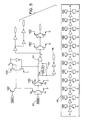
- Referring now to Fig. 5, a schematic diagram is shown of
RASGEN circuit 24 of Fig. 4. The RAS signal is applied viaterminal 22, to transistors Q2 and Q1 and then through transistors Q6 and Q5 tonode 3 and an input to NORcircuit 50. So long as a NOR condition is present at the inputs to NORcircuit 50, its output is at an active level. This causes the PRASBI, PRASBII, and PRASD signals to be at the high or inactive state. - For a three cycle memory operation, fuse 52 is blown, and causes a signal appearing at
node 3 to be applied throughdelay circuit 54 to an input to NORcircuit 50. (The details ofdelay circuit 54 are shown expanded at 56 in Fig. 5). Consequently, an active output atnode 5 from NORcircuit 50 is present only after the level atnode 3 transitions from the high state to the low state (indicating the termination of the RAS reset/precharge state) and that transition is delayed and arrives at NORcircuit 50 viadelay 54. - Since
node 3 has the same polarity asRAS input 22, the PRASD and PRASBII signals derived whennode 5 transitions to the active state, are activated at the end of the delayed RAS signal. In contrast, the PRASBI signal appearing atnode 58 is activated whennode 3 goes low and immediately causes the row addresses inrow address buffer 18 to be latched. - If a two cycle memory is employed, fuse 52 is not blown and the circuit operates as the prior art circuit shown in Fig. 2.
- In Fig. 6, a schematic diagram of row
address buffer circuit 18 is shown. The circuit is modification of a prior circuit shown in U.S. Patent 4,697,108 to Chappell et al. The modified portion is shown in dottedbox 60. The address true and complement signals appear atterminals terminal 64 throughNAND GATES terminal 66 is activated, the circuit latches the addresses appearing onrow address input 68. The address true and complement outputs onterminals terminal input 64 is asserted. - It can be seen from the above, that the RAS reset/precharge time is extended by an on-chip generated control signal derived from NOR
circuit 50 in Fig. 5. That output and its duration is controlled by the fall atnode 3 of the RAS signal and its time delay throughdelay circuit 54. Thus the extension by the delay circuit is only a fraction of the RAS reset time, thus enabling more accurate timing of the RAS cycle.
Claims (5)
Applications Claiming Priority (2)
| Application Number | Priority Date | Filing Date | Title |
|---|---|---|---|
| US545797 | 1990-06-29 | ||
| US07/545,797 US5185719A (en) | 1989-10-14 | 1990-06-29 | High speed dynamic, random access memory with extended reset/precharge time |
Publications (3)
| Publication Number | Publication Date |
|---|---|
| EP0468135A2 true EP0468135A2 (en) | 1992-01-29 |
| EP0468135A3 EP0468135A3 (en) | 1994-08-17 |
| EP0468135B1 EP0468135B1 (en) | 1997-05-28 |
Family
ID=24177584
Family Applications (1)
| Application Number | Title | Priority Date | Filing Date |
|---|---|---|---|
| EP19910104396 Expired - Lifetime EP0468135B1 (en) | 1990-06-29 | 1991-03-21 | A high speed dynamic, random access memory with extended reset/precharge time |
Country Status (3)
| Country | Link |
|---|---|
| EP (1) | EP0468135B1 (en) |
| JP (1) | JPH06103595B2 (en) |
| DE (1) | DE69126253D1 (en) |
Cited By (2)
| Publication number | Priority date | Publication date | Assignee | Title |
|---|---|---|---|---|
| GB2287112A (en) * | 1994-03-03 | 1995-09-06 | Samsung Electronics Co Ltd | Auto-precharging semiconductor memory devices |
| USRE36532E (en) * | 1995-03-02 | 2000-01-25 | Samsung Electronics Co., Ltd. | Synchronous semiconductor memory device having an auto-precharge function |
Families Citing this family (1)
| Publication number | Priority date | Publication date | Assignee | Title |
|---|---|---|---|---|
| US7166900B1 (en) * | 2005-08-17 | 2007-01-23 | Infineon Technologies Ag | Semiconductor memory device |
Citations (4)
| Publication number | Priority date | Publication date | Assignee | Title |
|---|---|---|---|---|
| US4602356A (en) * | 1981-12-02 | 1986-07-22 | Fujitsu Limited | Semiconductor memory device |
| US4831597A (en) * | 1986-11-25 | 1989-05-16 | Kabushiki Kaisha Toshiba | Dynamic random access semiconductor memory wherein the RAS and CAS strobes respectively select the bit line and word line pairs |
| US4833656A (en) * | 1986-11-11 | 1989-05-23 | Mitsubishi Denki Kabushiki Kaisha | Fast access circuit for dynamic type semiconductor memory device |
| US4905192A (en) * | 1987-03-31 | 1990-02-27 | Kabushiki Kaisha Toshiba | Semiconductor memory cell |
-
1991
- 1991-03-21 EP EP19910104396 patent/EP0468135B1/en not_active Expired - Lifetime
- 1991-03-21 DE DE69126253T patent/DE69126253D1/en not_active Expired - Lifetime
- 1991-05-15 JP JP3138640A patent/JPH06103595B2/en not_active Expired - Lifetime
Patent Citations (4)
| Publication number | Priority date | Publication date | Assignee | Title |
|---|---|---|---|---|
| US4602356A (en) * | 1981-12-02 | 1986-07-22 | Fujitsu Limited | Semiconductor memory device |
| US4833656A (en) * | 1986-11-11 | 1989-05-23 | Mitsubishi Denki Kabushiki Kaisha | Fast access circuit for dynamic type semiconductor memory device |
| US4831597A (en) * | 1986-11-25 | 1989-05-16 | Kabushiki Kaisha Toshiba | Dynamic random access semiconductor memory wherein the RAS and CAS strobes respectively select the bit line and word line pairs |
| US4905192A (en) * | 1987-03-31 | 1990-02-27 | Kabushiki Kaisha Toshiba | Semiconductor memory cell |
Cited By (3)
| Publication number | Priority date | Publication date | Assignee | Title |
|---|---|---|---|---|
| GB2287112A (en) * | 1994-03-03 | 1995-09-06 | Samsung Electronics Co Ltd | Auto-precharging semiconductor memory devices |
| GB2287112B (en) * | 1994-03-03 | 1998-07-29 | Samsung Electronics Co Ltd | Auto-precharging semiconductor memory devices |
| USRE36532E (en) * | 1995-03-02 | 2000-01-25 | Samsung Electronics Co., Ltd. | Synchronous semiconductor memory device having an auto-precharge function |
Also Published As
| Publication number | Publication date |
|---|---|
| DE69126253D1 (en) | 1997-07-03 |
| JPH04229482A (en) | 1992-08-18 |
| JPH06103595B2 (en) | 1994-12-14 |
| EP0468135A3 (en) | 1994-08-17 |
| EP0468135B1 (en) | 1997-05-28 |
Similar Documents
| Publication | Publication Date | Title |
|---|---|---|
| JP2851503B2 (en) | Integrated circuit storage device | |
| US6128237A (en) | Method and apparatus for enhancing the performance of semiconductor memory devices | |
| US5636174A (en) | Fast cycle time-low latency dynamic random access memories and systems and methods using the same | |
| US7349277B2 (en) | Method and system for reducing the peak current in refreshing dynamic random access memory devices | |
| JP3140461B2 (en) | Random access memory | |
| US6463002B2 (en) | Refresh-type memory with zero write recovery time and no maximum cycle time | |
| US4943944A (en) | Semiconductor memory using dynamic ram cells | |
| US5185719A (en) | High speed dynamic, random access memory with extended reset/precharge time | |
| KR940008882B1 (en) | Random access memory of integrated circuit | |
| US5293347A (en) | Semiconductor memory device having read/write operation improved in pipe line processing | |
| US7821831B2 (en) | Block erase for volatile memory | |
| US6130843A (en) | Method and circuit for providing a memory device having hidden row access and row precharge times | |
| CA2313954A1 (en) | High speed dram architecture with uniform latency | |
| JPH0793009B2 (en) | Semiconductor memory device | |
| JPH07176186A (en) | Dynamic random-access memory and its refreshing method | |
| US5563835A (en) | Sense amplification in data memories | |
| JPS6213758B2 (en) | ||
| US4581722A (en) | Dynamic random access memory having small cycle time period | |
| US6108254A (en) | Dynamic random access memory having continuous data line equalization except at address transition during data reading | |
| US6205069B1 (en) | Semiconductor memory device with fast input/output line precharge scheme and method of precharging input/output lines thereof | |
| EP0037252B1 (en) | Dynamic semiconductor memory | |
| US6456563B1 (en) | Semiconductor memory device that operates in sychronization with a clock signal | |
| US5007028A (en) | Multiport memory with improved timing of word line selection | |
| US4354259A (en) | Semiconductor memory device having improved column selection structure | |
| EP0468135B1 (en) | A high speed dynamic, random access memory with extended reset/precharge time |
Legal Events
| Date | Code | Title | Description |
|---|---|---|---|
| PUAI | Public reference made under article 153(3) epc to a published international application that has entered the european phase |
Free format text: ORIGINAL CODE: 0009012 |
|
| AK | Designated contracting states |
Kind code of ref document: A2 Designated state(s): DE FR GB |
|
| 17P | Request for examination filed |
Effective date: 19911219 |
|
| PUAL | Search report despatched |
Free format text: ORIGINAL CODE: 0009013 |
|
| AK | Designated contracting states |
Kind code of ref document: A3 Designated state(s): DE FR GB |
|
| 17Q | First examination report despatched |
Effective date: 19960110 |
|
| GRAG | Despatch of communication of intention to grant |
Free format text: ORIGINAL CODE: EPIDOS AGRA |
|
| GRAH | Despatch of communication of intention to grant a patent |
Free format text: ORIGINAL CODE: EPIDOS IGRA |
|
| GRAH | Despatch of communication of intention to grant a patent |
Free format text: ORIGINAL CODE: EPIDOS IGRA |
|
| GRAA | (expected) grant |
Free format text: ORIGINAL CODE: 0009210 |
|
| AK | Designated contracting states |
Kind code of ref document: B1 Designated state(s): DE FR GB |
|
| PG25 | Lapsed in a contracting state [announced via postgrant information from national office to epo] |
Ref country code: FR Free format text: THE PATENT HAS BEEN ANNULLED BY A DECISION OF A NATIONAL AUTHORITY Effective date: 19970528 |
|
| REF | Corresponds to: |
Ref document number: 69126253 Country of ref document: DE Date of ref document: 19970703 |
|
| ET | Fr: translation filed | ||
| PG25 | Lapsed in a contracting state [announced via postgrant information from national office to epo] |
Ref country code: DE Effective date: 19970829 |
|
| PG25 | Lapsed in a contracting state [announced via postgrant information from national office to epo] |
Ref country code: GB Free format text: LAPSE BECAUSE OF NON-PAYMENT OF DUE FEES Effective date: 19980321 |
|
| PLBE | No opposition filed within time limit |
Free format text: ORIGINAL CODE: 0009261 |
|
| STAA | Information on the status of an ep patent application or granted ep patent |
Free format text: STATUS: NO OPPOSITION FILED WITHIN TIME LIMIT |
|
| 26N | No opposition filed | ||
| GBPC | Gb: european patent ceased through non-payment of renewal fee |
Effective date: 19980321 |
|
| REG | Reference to a national code |
Ref country code: FR Ref legal event code: ST |