EP0474471A2 - Fixed frequency single ended forward converter switching at zero voltage - Google Patents
Fixed frequency single ended forward converter switching at zero voltage Download PDFInfo
- Publication number
- EP0474471A2 EP0474471A2 EP91308081A EP91308081A EP0474471A2 EP 0474471 A2 EP0474471 A2 EP 0474471A2 EP 91308081 A EP91308081 A EP 91308081A EP 91308081 A EP91308081 A EP 91308081A EP 0474471 A2 EP0474471 A2 EP 0474471A2
- Authority
- EP
- European Patent Office
- Prior art keywords
- switch
- switching means
- voltage
- main
- transformer
- Prior art date
- Legal status (The legal status is an assumption and is not a legal conclusion. Google has not performed a legal analysis and makes no representation as to the accuracy of the status listed.)
- Granted
Links
Images


Classifications
-
- H—ELECTRICITY
- H02—GENERATION; CONVERSION OR DISTRIBUTION OF ELECTRIC POWER
- H02M—APPARATUS FOR CONVERSION BETWEEN AC AND AC, BETWEEN AC AND DC, OR BETWEEN DC AND DC, AND FOR USE WITH MAINS OR SIMILAR POWER SUPPLY SYSTEMS; CONVERSION OF DC OR AC INPUT POWER INTO SURGE OUTPUT POWER; CONTROL OR REGULATION THEREOF
- H02M3/00—Conversion of dc power input into dc power output
- H02M3/22—Conversion of dc power input into dc power output with intermediate conversion into ac
- H02M3/24—Conversion of dc power input into dc power output with intermediate conversion into ac by static converters
- H02M3/28—Conversion of dc power input into dc power output with intermediate conversion into ac by static converters using discharge tubes with control electrode or semiconductor devices with control electrode to produce the intermediate ac
- H02M3/325—Conversion of dc power input into dc power output with intermediate conversion into ac by static converters using discharge tubes with control electrode or semiconductor devices with control electrode to produce the intermediate ac using devices of a triode or a transistor type requiring continuous application of a control signal
- H02M3/335—Conversion of dc power input into dc power output with intermediate conversion into ac by static converters using discharge tubes with control electrode or semiconductor devices with control electrode to produce the intermediate ac using devices of a triode or a transistor type requiring continuous application of a control signal using semiconductor devices only
- H02M3/33561—Conversion of dc power input into dc power output with intermediate conversion into ac by static converters using discharge tubes with control electrode or semiconductor devices with control electrode to produce the intermediate ac using devices of a triode or a transistor type requiring continuous application of a control signal using semiconductor devices only having more than one ouput with independent control
-
- H—ELECTRICITY
- H02—GENERATION; CONVERSION OR DISTRIBUTION OF ELECTRIC POWER
- H02M—APPARATUS FOR CONVERSION BETWEEN AC AND AC, BETWEEN AC AND DC, OR BETWEEN DC AND DC, AND FOR USE WITH MAINS OR SIMILAR POWER SUPPLY SYSTEMS; CONVERSION OF DC OR AC INPUT POWER INTO SURGE OUTPUT POWER; CONTROL OR REGULATION THEREOF
- H02M3/00—Conversion of dc power input into dc power output
- H02M3/22—Conversion of dc power input into dc power output with intermediate conversion into ac
- H02M3/24—Conversion of dc power input into dc power output with intermediate conversion into ac by static converters
- H02M3/28—Conversion of dc power input into dc power output with intermediate conversion into ac by static converters using discharge tubes with control electrode or semiconductor devices with control electrode to produce the intermediate ac
- H02M3/325—Conversion of dc power input into dc power output with intermediate conversion into ac by static converters using discharge tubes with control electrode or semiconductor devices with control electrode to produce the intermediate ac using devices of a triode or a transistor type requiring continuous application of a control signal
- H02M3/335—Conversion of dc power input into dc power output with intermediate conversion into ac by static converters using discharge tubes with control electrode or semiconductor devices with control electrode to produce the intermediate ac using devices of a triode or a transistor type requiring continuous application of a control signal using semiconductor devices only
- H02M3/33569—Conversion of dc power input into dc power output with intermediate conversion into ac by static converters using discharge tubes with control electrode or semiconductor devices with control electrode to produce the intermediate ac using devices of a triode or a transistor type requiring continuous application of a control signal using semiconductor devices only having several active switching elements
-
- H—ELECTRICITY
- H02—GENERATION; CONVERSION OR DISTRIBUTION OF ELECTRIC POWER
- H02M—APPARATUS FOR CONVERSION BETWEEN AC AND AC, BETWEEN AC AND DC, OR BETWEEN DC AND DC, AND FOR USE WITH MAINS OR SIMILAR POWER SUPPLY SYSTEMS; CONVERSION OF DC OR AC INPUT POWER INTO SURGE OUTPUT POWER; CONTROL OR REGULATION THEREOF
- H02M3/00—Conversion of dc power input into dc power output
- H02M3/01—Resonant DC/DC converters
Definitions
- This invention relates to DC-to-DC converters, and relates more specifically to forward single ended converters which switch at zero voltage and to methods of operating such converters.
- a DC-to-DC converter is a circuit which converts a direct current voltage at one level to a direct current voltage at another level. If the circuit is based upon switching the input DC current through the primary of a transformer and then rectifying it in the secondary of the transformer, the converter is called a single ended forward converter.
- a single ended forward converter is gated by a single switch in series with the primary of the transformer. Energy is transferred forward from the input through the primary winding to the secondary winding of the transformer during the ON period of the switch.
- Common prior art DC-to-DC converter topologies include the buck or forward converter, the buck-boost or flyback converter, and the boost converter which transfer energy from the input to the output during the ON time or OFF time of the main switch. In these circuits a dead time is created during the energy transfer which results in an increase in size of an output filter. Barthold combines the forward and flyback topologies to achieve a continuous transfer of energy from the input to the output of the converter to significantly reduce the size of the output filter.
- the prior art has devised a new family of resonant and quasi-resonant DC-to-DC converters.
- the prior art technique consists of shaping the current or voltage to become half sinusoidal and to perform the switching when the current or voltage reaches zero.
- the reactive elements which contribute to shaping the current or voltage are part of the basic circuit and are considered undesirable in classic topologies because of leakage inductance and parasitic capacitance.
- An example of one such circuit can be found in Vinciarelli, "Forward Converter Switching at Zero Current", U.S. Patent 4,415,959.
- the technique utilised by Vinciarelli consists of adding a resonant capacitor across the flywheeling diode to create a resonant circuit in combination with the leakage inductance of the transformer.
- a current charges the resonant capacitor.
- the main switch turns OFF in the primary of the transformer.
- the output inductor discharges the resonant capacitor, transferring the energy to the load.
- This topology eliminates switching losses which allows the converter to run at a very high frequency.
- this topology exhibits several drawbacks which limit its utilisation at low and medium power levels. These drawbacks are as follows.
- the peak current in such a quasi-resonant converter is significantly higher than in a conventional forward converter.
- the peak current becomes substantially large if a large input voltage range is required.
- the energy in the prior art device is transferred in stages from the input to the resonant capacitor and then from the resonant capacitor to the output. Due to the fact that the switching in the primary occurs at zero current and non-zero voltage, the energy contained in the output capacitance of the main switch is dissipated when it turns ON.
- Output power is varied by varying the frequency. A certain amount of energy is transferred from the input to the output at every cycle and when the power requirements are high, the repetition frequency is correspondingly high. Modulation of the frequency does not allow significant decrease of the output filter size.
- a large electromagnetic interference (EMI) filter is required to avoid beat frequency problems between the units, if two non-synchronised units are used together.
- An additional group of quasi-resonant converters includes the multi-resonant converters such as were described at the High Frequency Power Conversion International Proceedings (May, 1988), Intertec Communications, Ventura, California. While operating similarly to other quasi-resonant topologies, a secondary resonant circuit is employed to decrease the stress across the output rectifier and to reduce frequency swings over various input-output conditions of operation.
- the invention utilises a topology which uses energy accumulated in the magnetic field of the isolation transformer to discharge the output capacitance of the main switch to zero.
- the magnetising energy within the isolation transformer was either recycled back to the input source or in some cases dissipated in a snubber resistor.
- the discharge of the capacitance of the main switch to zero prior to TURN ON of the main switch has several advantages. For example, losses caused by energy stored in the output capacitance of the main switch are eliminated since they are internally dissipated when the main switch is turned on. Switching noise from the Miller effect is eliminated. Current spikes generated at TURN ON of the main switch due to parasitic capacitance of the transformer is eliminated.
- a low time rate of change of the voltage arising from the quasi-resonant discharge of the capacitance of the main switch is reflected as a low rate of change of voltage across the secondary windings. This significantly reduces the current spike across the secondary windings of the transformer due to cross conduction between the main rectifying diode and the flywheeling diode in the output stage. A slow rate of change of the voltage allows the flywheel diode to recover from conduction.
- a saturable reactor is used in the secondary circuit of the transformer to delay the current flow and cross conduction between the flywheel diode and the main diode is further reduced.
- the power transfer to the output is modulated by varying the duty cycle, as is commonly used in constant frequency converters.
- the main switch is turned OFF prior to the voltage being built up across it. This is accomplished by a fast TURN OFF scheme and also by using an external capacitor connected across the main switch. Energy accumulated in the capacitor is not discharged through the main switch, but is cycled back to the input source.
- the energy contained in the leakage inductance of the transformer is not dissipated but is also recycled back to the input source.
- Another advantage of the topology of the invention is its ability to reset the transformer to eliminate the DC component from the flux density in the transformer. This leads to better utilisation of the core of the transformer for a single ended forward converter.
- One consequence of this resetting technique is the minimisation of the voltage stress on the primary switch. A constant voltage is applied across the primary switch during the OFF time which is tailored to avoid the dead time.
- the duty cycle is not limited to a 50% constraint which is imposed by most prior art resetting techniques.
- the condition necessary to achieve zero voltage switching is also independent of the output current.
- prior art, zero current crossing, resonant converters limit the output current in order to achieve a zero current crossing condition.
- switching losses are virtually eliminated; noise in the primary and secondary of the isolation transformer is significantly decreased; the available flux swing for the isolation transformer is maximised; the voltage across the main switch is minimised; limitations on the main switch duty cycle due to transformer core saturation are avoided; constraints on the output current due to zero voltage conditions are avoided; the ability to provide multiple outputs is provided; the circuit is adaptable to primary current mode control; the circuit is operable at very high frequencies without switching losses or noise; the circuit is capable of high power density conversion due to full utilisation of the transformer core, high frequency operation and constant frequency operation thereby minimising the size of the output filter; and the circuit does not require special components typical of resonant capacitors with very low equivalent series resistance.
- a single ended, zero-voltage switching, forward DC-to-DC converter is characterised by a DC voltage source and a transformer having a primary and secondary winding.
- a main switch selectively couples the voltage source across the primary winding of the transformer.
- An auxiliary switch selectively allows the voltage across the primary winding to reach zero.
- the main switch and auxiliary switch each have an OFF period and ON period.
- the auxiliary switch is non-conductive prior to the ON period of the primary switch by a predetermined time period sufficient to allow the voltage across the primary switch circuit to reach zero voltage.
- the auxiliary switch remains non-conductive until the main switch cycles through its corresponding ON period and OFF period.
- a reset capacitor is coupled between the auxiliary switch and AC ground of the converter.
- a third switch is coupled in series with the secondary winding of the transformer and selectively remains at least partially non-conductive as the voltage across the primary switch reaches decreases. The third switch becomes conductive when the voltage across the primary switch reaches zero.
- a first rectifier is coupled in series with the third switch for conducting current from the third switch.
- a control circuit selectively operates the main switch, the auxiliary switch and third switch to transfer energy through the converter by modification of the duty cycle of operation of at least the main and auxiliary switch to achieve turn ON of the primary switch at zero voltage.
- the converter further comprises a discrete, resonant capacitor in parallel with the primary switch.
- converter further comprising an inductor coupled in parallel across the primary winding of the transformer in series circuit with the auxiliary switch and the reset capacitor.
- first rectifier and the third switch comprise a unidirectionally controlled switch circuit.
- the unidirectional controlled switch circuit is selectively operated by the control circuit so that it is non-conductive after the voltage across the primary switch reaches zero, and so that it is conductive during the corresponding ON time of the primary switch.
- the transformer comprises a plurality of secondary windings.
- the third switch is a saturable reactor.
- the converter further comprises a load and load inductor.
- the load inductor is coupled in series circuit between the first rectifier, third switch and load.
- the converter further comprises a second rectifier coupled between ground of the secondary winding of the transformer and the input to the load inductor at its coupling to the first rectifier.
- the control circuit comprises a sensory circuit for sensing voltage across the load.
- the control circuit maintains a constant voltage across the load by varying the ON period of the primary switch, the third switch or both.
- the third switch is a saturable inductor or a synchronised rectifier.
- the converter further comprises a voltage reference.
- the control circuit compares the difference in voltage across the load and the voltage reference. The difference is compared to a signal which is proportional to the current through the primary switch.
- the converter further comprises a second transformer having a corresponding primary winding and secondary winding.
- the third switch comprises the secondary winding of the secondary transformer, and the control circuit applies a variable voltage to the primary winding of the secondary transformer.
- a single ended forward converter in which energy is transferred from a primary winding to a secondary winding of a transformer during an ON period of a primary switch.
- Circuitry is provided for recycling the magnetising energy stored in the transformer to reset it during the OFF period of the primary switch such that discharge of output capacitance of the primary switch to zero is achieved prior to turn ON of the primary switch on a subsequent cycle.
- the invention comprises a reset capacitor.
- An auxiliary switch including an antiparallel diode is coupled in series with the reset capacitor.
- a switch control circuit operates the auxiliary switch including the antiparallel diode in accordance with a control logic such that:
- the auxiliary switch may comprise a field effect transistor in parallel with a discrete and/or body diode.
- the converter further comprises a circuit for inhibiting current in the secondary winding of the transformer until the output capacitance of the primary switch is discharged.
- a method of operating a single ended forward DC-to-DC converter characterised by the steps of storing energy in a primary winding of a transformer by flowing DC current through the primary winding in series circuit with a primary switch.
- the primary switch is then turned OFF.
- a secondary switch in series circuit with the primary of the transformer is turned on to charge a reset capacitor.
- the secondary switch is turned on after the primary switch turns off. After the charge on the reset capacitor is increased to a predetermined level, the secondary switch is turned off.
- the current flow through the primary winding reverses and allows the output capacitance of the primary switch to discharge into the input source.
- the voltage across the primary switch is thus drawn down to zero, thereby allowing the primary switch to then turn on at zero voltage.
- Voltage discharge across the primary switch is implemented in part and facilitated by selective opening of a third switch in series with the secondary winding of the transformer.
- a single ended forward DC-to-DC converter is operated with a primary switch connected in series with a primary winding of an isolation transformer and an auxiliary switch for charging a reset capacitor also in circuit with the primary winding.
- the primary switch and the auxiliary switch are operated through control logic so that neither switch is ON at the same time.
- a predetermined dead time is provided between turning OFF the auxiliary switch and turning ON the primary switch to allow the output capacitance of the primary switch to discharge into the input source.
- Current discharge into the secondary of the transformer during this time period is limited by a third switch, which may either be a saturable reactor in series circuit with the secondary, or a selectively controlled switch.
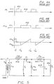
- switch 12 shown in Figure 3a symbolically as a mechanical switch, but which in practice always assumes the form of a semiconductor switch, is open.
- Primary switch 10, S1 is closed starting with the first ON period 20 in Figure 4.
- the DC voltage Vin is impressed upon the primary winding 16 of transformer 18 causing a magnetic flux to be propagated across the core 22 of the transformer. If N is the number of primary turns, the total change in flux is Vin(T2-T1)/N.
- the change in magnetising current is then given by Vin (T2-T1)/Lm where Lm is the magnetising inductance of transformer 18.
- switch 10, S1 turns OFF and switch 12, S2, turns ON.
- Current then flows into capacitor 24.
- the energy stored in the magnetising inductance of transformer 18 is then transferred into capacitor 24.
- Vr which is a function of the input voltage, Vin, and the duty cycle of switch 12, S2.
- the resonant frequency defined by capacitor 24 and the magnetising inductance Lm is assumed to be much lower than the repetition frequency at which switches 12 and 10 are opened and closed.
- the voltage across capacitor 24 does not change during the OFF period 26 of switch 10, S1, as shown in Figure 4 or conversely the ON time of switch 12,S2.
- Vr i.e. the resetting voltage across capacitor 24
- the magnetising energy of transformer 18 is used to discharge the output capacitance of switch 10 instead of cycling it back and forth between the input source and capacitor 24.
- switches 10 and 12 are very critical within the circuit of Figure 3a. Particular problems arise if switch 12 does not turn OFF prior to the turn ON of switch 10. Cross-conduction between switches 10 and 12 leads to very high current spikes limited only by the conductive resistance of switches 10 and 12. Avoidance of cross conduction in a forward converter with a capacitive reset switch has long been known and the use of out-of-phase switches in the primary loop for this purpose is shown by Polikarpov et. al., "Single-Cycle Direct Voltage Regulator", Soviet Patent SU 892-614 (1981). As will be described below, according to the present invention, a predetermined delay T is used to steer the magnetising current in order to discharge the output capacitance of the FET.
- Peak magnetising current which is a significant portion of the primary current in transformer 18, is kept under a predetermined level which is below saturation of the core.
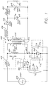
- FIG. 1 illustrates the methodology of the invention it will be seen that ideal switches 10 and 12 of Figure 3a are replaced by MOSFET devices 30 and 32 which are the preferred choice because of the existance within such devices of body diodes 34 and 36, respectively, to provide a reverse current flow through the switch without an additional external diode.
- the circuit equivalent of the actual MOSFET devices has been illustrated within a dotted outline.
- the body diodes 36 and 34 thus represent the parasitic diode within the actual MOSFET.
- transformer 48 is illustrated within a corresponding dotted outline and includes the parasitic magnetisation inductance Lm and the load inductance Ld.
- Control signals VS1 and VS2 are provided to the gates of MOSFETs 32 and 34 from a control circuit, the timing of which is described below in connection with Figure 2 and which is itself described later in greater detail in connection with Figures 7 and 9.
- MOSFETs 32 and 34 are controlled sot hat there is a predetermined time interval, T, between the turn OFF of switch 32 and the turn ON of main or primary switch 30. At the moment when reset switch 32 turns OFF, the current flowing through it flows from storage capacitor 38 through the magnetising inductance 40, Lm, and input load inductance 42, Ld, toward the input voltage source 44, Vin.
- the magnetising current tries to continue its flow by flowing through capacitor 46, magnetising inductance 40 and load inductance 42 toward the input voltage source 44.
- the excess energy stored within the magnetic field in transforemr 48 causes body diode 34 to conduct and allows zero voltage switching to occur in switch 30.
- the timing delay between the switching cycles of switches 30 and 32, as shown by T in timing lines 68 and 74 of Figure 2, is solely determined by the discharge path characteristics from switch 30 through the inductance of transformer 48 to input source 44. This in turn is affected by a third switch 56 described below.
- the corresponding increment in the current flowing through the magnetisation inductance Lm is DTVIN/Lm where D is the duty cycle and T is a repetition period.
- the magnetising current, Im then is one half this value.
- the left side of the inequality is the resonant frequency of the magnetising current and the output capacitance of switch 30, which will be re-designated as a single quantity "f", the resonant frequency.
- the inequality can then be restated as: f D(1-D) > Fr.
- the resonant frequency, f of the circuit should be selected to satisfy the inequality (1) specified above over all input and output conditions. Since the output capacitance of switch 30 is a fixed factor due to the MOSFET structure, only the magnetising inductance can be varied to set the resonant frequency.
- Transformer 48 comprises a primary coil 50 and secondary coil 52 with a magnetising core 54.
- Secondary coil 52 is in series circuit with a saturable inductor 56 and main diode 58.
- the output of the circuit is provided to a load inductance 60, a load resistance 66 and load capacitance 64, the latter two of which are in parallel with each other.
- a flywheel diode 62 is also coupled across the output.
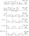
- Graph line 68 corresponds to the gate voltage applied to main switch 30 illustrating ON state periods 70 and OFF state periods 72.
- Graph line 74 similarly corresponds to the gate voltage applied to secondary switch 32.
- OFF periods 76 are alternated with ON state periods 78.
- a time gap T or "dead" time is provided between T1 and T2 following an ON state 78 of secondary switch 32 and before ON state 70 of main switch 30.
- I is determined by the discharge time of switch 30.
- Graph line 84 represents the current through main switch 30.
- the current through saturable inductor 56 is represented on graph line 86 as will be described in greater detail below.
- the voltage differential across the secondary 52 of transformer 48 is depicted by graph line 88.
- the timing relationships of the input and output voltages and currents in the primary and secondary windings of transformer 48 are illustrated by graph lines 80-88 of Figure 2.
- positive current flows in switch 30 only after the voltage across switch 30 reaches zero.
- graph line 88 the slope of the rising edge of the voltage across the secondary winding is decreased in proportion to the slope of the falling edge of the voltage across switch 30 as seen from graph line 80, so that ringing in the secondary is significantly decreased.
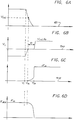
- FIG. 6 is a timing diagram which shows the relationship of several signals and the output of the circuit of Figure 1 as shown in Figure 5.
- Graph line 81 represents the voltage across main switch 30.
- the voltage across both saturable inductor 56 and secondary 52 is represented by the graph line 90 in Figure 6.
- the current through the saturable inductor, Ils, and the current flowing through flywheel diode 62 are shown on graph line 92.
- auxiliary switch 32 turns OFF as shown in Figure 2 and the magnetising current starts to flow from the output capacitance of main switch 30, here primarily due to the capacitance of capacitor 46.
- This current is represented by graph line 84 in Figure 2.
- the voltage across main switch 30 is shown in enlarged time scale on graph line 81 of Figure 6.
- Vin the input voltage
- the voltage reflected in secondary coil 52 reaches zero as depicted on graph line 88 of Figure 2.
- the voltage across secondary coil 52 thereafter is in the process of becoming positive.
- main diode 58 would be forward biased and the current would flow into the secondary circuit, thereby transferring part of the energy contained in the magnetic field created by the magnetising current to the secondary of the circuit. If this were to occur, it would not allow enough magnetising energy to be returned to the input source to discharge the output capacitance of main switch 30 and thus obtain zero voltage switching. To prevent this, saturable inductor 56, LS, is included in series circuit within the secondary output.
- inductor 56 For low level currents through saturable inductor 56, inductor 56 exhibits high inductance. Once the current flowing through it reaches a predetermined level, inductor 56 saturates and effectively becomes an electrical short circuit.
- the time delay introduced by saturable inductor 56 is chosen to be larger than the time difference T3-T2 in Figure 6, which is the time interval during which the voltage across main switch 30 decreases from Vin to zero.
- Graph line 92 shows that little current flows through saturable inductor 56 until T3 is approached.
- the exponential shape of the current of the saturable reactor as shown by graph line 92 is typical of its saturable characteristic.
- Graph line 90 is representative of the voltage between the anodes of main diode 58 and flywheel diode 62.
- Main diode 58 is back biased until at least time T2 and until current begins to flow through saturable inductor 56 at about time T3.
- the voltage then applied to the anode of main diode 58 is the input voltage multiplied by the turns ratio of transformer 48.
- time delay exhibited by saturable inductor 56 could be replaced by a synchronised switch which turns on after the voltage of main switch 30 reaches zero.
- main or primary switch 30 and auxiliary switch 32 are gated by external control signals which are derived through conventional control circuitry.
- a control circuit according to the invention is described in connection with Figures 7 and 8. Turning to the schematic circuit diagram of Figure 7, the circuit of Figure 1 is shown as controlled through a current mode control.
- an inner feedback loop controls the flux density in main transformer 48 by controlling the peak current. This eliminates the risk of saturation of the transformer core during transients which are associated with this resetting technique.
- the lack of current ringing at turn ON of main switch 30 at zero voltage and the presence of a gentle slope of the magnetising current as shown on graph line 84 of Figure 2 makes current mode control implementation more effective and easier.
- main switch 30 is shown as resistively coupled to ground through resistor 94 for current mode control
- the gate of main switch 30 is driven by latch 96 which is set by a clock 98.
- Latch 96 is reset by the output of a comparator 100.
- the inputs to comparator 100 are the voltage between the series combination of main switch 30 and resistor 94 on one hand, and the output of an error amplifier 102 on the other.
- Error amplifier 102 is a differential amplifier operating between a reference voltage and the output voltage coupled fromt he secondary circuit, namely the output load inductance 60.
- the output of latch 96 is also used as a trigger signal for reset logic circuit 104.
- the gate of secondary transistor 32 is driven by reset logic circuit 104.
- Secondary or auxiliary switch 32 is in parallel with an anti-parallel diode 106.
- Anti-parallel diode 106 includes both internal and external diodes to transistor 32.
- An anti-parallel diode is defined for the purposes of this specification as a diode coupled in parallel with a switch, wherein the direction of current flow through the diode is opposite to the normal direction of current flow through the switch.
- FIG 8 is the timing diagram of the circuit of Figure 7.
- Graph line 108 illustrates the clock pulses generated by clock circuit 98 provided as the set signal to latch 96.
- the output of latch 96 is depicted on graph line 110.
- the voltage sensed from resistor 94 is indicated by pulses 112 on graph line 114.
- the output of error amplifier 102 is a constant voltage level, V error , depending upon the difference, if any, between the reference voltage and the output voltage.
- comparator 100 When V error and the voltage at resistor 94 at the output of main switch 30 is equal, comparator 100 generates a trigger pulse which resets latch 96 as shown on graph line 110.
- the latch output is set by clock circuit 98.
- the latch output shown on graph line 110 is used to drive the gate of main switch 30.
- the same output is provided to reset logic circuit 104 for driving auxiliary switch 32 according to the teachings of the invention.
- the gate drive of auxiliary switch 32 will be complemented and delayed in a manner similar to that described
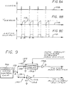
- FIG. 9 shows a simplified block diagram for generating timing signals of the invention, this has a corresponding timing diagram shown in Figure 10.
- the current mode control output from latch 96 is shown by graph line 114 in Figure 10 and is provided at output 116 of latch 96 in Figure 9.
- the time period between latch output pulses 118 is T.
- Pulse 118 is coupled in common to a rise time delay, generally denoted by reference numeral 120, and a fall time delay 122.
- the voltage at node 124 is depicted by graph line 126 in Figure 10 while the voltage at node 128 is depicted by graph line 130.
- the filtered pulses shown on graph line 120 are then input into inverter and driver 132 whose output is depicted on graph line 134 of Figure 10. These pulses are provided to auxiliary switch 32 and are delayed by time dT1 after the all of the voltage at 124.
- the pulses depicted on graph line 130 may then be input into a conventional controlled delay circuit 136.
- the amount of delay introduced by delay circuit 136 into the pulse can be varied according to a signal which is representative of the voltage across main switch 30.
- the output of controlled delay circuit 136 is then coupled through a buffer 138 and is depicted on graph line 140.
- the delay dT2 is controlled according to the voltage across main switch 30 and is provided to ensure that there is a gap or dead time between the gating signal provided to switches 30 and 32 to ensure the operation of the device as previously described in connection with Figures 2 and 6. It must be clearly understood that many other types of controllers can be utilised for timing in addition to those illustratively set forth here.
- FIG. 11 Another embodiment of the invention similar to that described in Figure 7 is schematically illustrated in Figure 11 where a plurality of secondary coils 52(1)-52(m) are included within transformer 48, each with a corresponding secondary output circuit.
- Each of the secondary circuits in Figure 11 has its own third switch 56(1)-56(m), which is shown in each case as a saturable inductor.
- the first secondary circuit corresponding to coil 52(1) is provided with the feedback control described in Figure 7 through control circuit 140.
- Each of the other secondary circuits corresponding to coils 52(2)-52(m) have separate corresponding control circuits 140(2)-140(m) in the secondary circuit to individually set each output circuit.
- FIG. 12 shows a circuit similar to that shown in Figure 11 but in which the saturable inductor of the secondary circuit corresponding to coil 52(1) has been removed and a synchronised switch 142 has been substituted in lieu thereof.
- Switch 142 is controlled by control circuit 144 according to the teachings of the invention to effect a zero voltage switching, which control circuit also provides the feedback control from the secondary output circuit to the primary output circuit as shown in Figures 7 and 11.
- any kind of switch now known or later devised may be used, including N or P type FET power devices which may be substituted for the main and auxiliary switches, the carrier type of the main and auxiliary switches may be interchanged with each other, and the reset capacitor may be connected to the positive source or return.
Abstract
Description
- This invention relates to DC-to-DC converters, and relates more specifically to forward single ended converters which switch at zero voltage and to methods of operating such converters.
- A DC-to-DC converter is a circuit which converts a direct current voltage at one level to a direct current voltage at another level. If the circuit is based upon switching the input DC current through the primary of a transformer and then rectifying it in the secondary of the transformer, the converter is called a single ended forward converter. A single ended forward converter is gated by a single switch in series with the primary of the transformer. Energy is transferred forward from the input through the primary winding to the secondary winding of the transformer during the ON period of the switch.
- One of the main design goals in such DC-to-DC converters is to increase the amount of power transferred through the converter. One prior art approach is presented by Fred O.Barthold in "Source Volt-Ampere/Load Volt-Ampere Differential Converter", U.S. Patent.
- Common prior art DC-to-DC converter topologies include the buck or forward converter, the buck-boost or flyback converter, and the boost converter which transfer energy from the input to the output during the ON time or OFF time of the main switch. In these circuits a dead time is created during the energy transfer which results in an increase in size of an output filter. Barthold combines the forward and flyback topologies to achieve a continuous transfer of energy from the input to the output of the converter to significantly reduce the size of the output filter.
- Another prior art method for increasing the power transfer through the converter is to increase the switching frequency. This results in a reduction of the size of the isolation transformer and the output filter. However, there are upper limits to the operating frequency of prior art buck converters, for example, on account of switching losses in the semiconductor switches utilised in the converters. Switching losses occur when the main semiconductor switch in the buck converter is turned ON and OFF due to the finite switching speed or the time required for the current in the semiconductor device to start and stop flowing.
- In order to overcome limitations in switching speeds, the prior art has devised a new family of resonant and quasi-resonant DC-to-DC converters. In the case of quasi-resonant converters, the prior art technique consists of shaping the current or voltage to become half sinusoidal and to perform the switching when the current or voltage reaches zero. The reactive elements which contribute to shaping the current or voltage are part of the basic circuit and are considered undesirable in classic topologies because of leakage inductance and parasitic capacitance. An example of one such circuit can be found in Vinciarelli, "Forward Converter Switching at Zero Current", U.S. Patent 4,415,959. The technique utilised by Vinciarelli consists of adding a resonant capacitor across the flywheeling diode to create a resonant circuit in combination with the leakage inductance of the transformer. During the ON time of the main switch, a current charges the resonant capacitor. When the current reaches zero, the main switch turns OFF in the primary of the transformer. The output inductor discharges the resonant capacitor, transferring the energy to the load. This topology eliminates switching losses which allows the converter to run at a very high frequency. However, this topology exhibits several drawbacks which limit its utilisation at low and medium power levels. These drawbacks are as follows.
- The peak current in such a quasi-resonant converter is significantly higher than in a conventional forward converter. The peak current becomes substantially large if a large input voltage range is required. The energy in the prior art device is transferred in stages from the input to the resonant capacitor and then from the resonant capacitor to the output. Due to the fact that the switching in the primary occurs at zero current and non-zero voltage, the energy contained in the output capacitance of the main switch is dissipated when it turns ON. Output power is varied by varying the frequency. A certain amount of energy is transferred from the input to the output at every cycle and when the power requirements are high, the repetition frequency is correspondingly high. Modulation of the frequency does not allow significant decrease of the output filter size. A large electromagnetic interference (EMI) filter is required to avoid beat frequency problems between the units, if two non-synchronised units are used together.
- Another family of quasi-resonant converters which switch at zero voltage is described by F.C.Lee, "Pulse Width Modulation Technique", High Frequency Power Conversion International Proceedings (April 1987), Intertec Communications, Ventura, California. These prior art circuits operate similarly to those described above with the exception that the main switch turns ON and OFF at zero voltage. This has the advantage of eliminating the losses caused by the discharge of the capacitance of the switch at turn on and also decreases the driving current utilised in the MOSFET switch due to elimination of the Miller effect, i.e. induced increase in capacitance due to anode-to-cathode charging.
- However, the voltage stress across the main switch and the frequency modulation which is required make this topology unattractive.
- An additional group of quasi-resonant converters includes the multi-resonant converters such as were described at the High Frequency Power Conversion International Proceedings (May, 1988), Intertec Communications, Ventura, California. While operating similarly to other quasi-resonant topologies, a secondary resonant circuit is employed to decrease the stress across the output rectifier and to reduce frequency swings over various input-output conditions of operation.
- What is needed is a converter which can operate a constant frequency yet eliminates current or voltage stresses which are characteristic of prior art quasi-resonant converters while at the same time shaping the voltage or current only at the switching time.
- The invention utilises a topology which uses energy accumulated in the magnetic field of the isolation transformer to discharge the output capacitance of the main switch to zero. In contrast, in the prior art technologies the magnetising energy within the isolation transformer was either recycled back to the input source or in some cases dissipated in a snubber resistor. The discharge of the capacitance of the main switch to zero prior to TURN ON of the main switch has several advantages. For example, losses caused by energy stored in the output capacitance of the main switch are eliminated since they are internally dissipated when the main switch is turned on. Switching noise from the Miller effect is eliminated. Current spikes generated at TURN ON of the main switch due to parasitic capacitance of the transformer is eliminated. A low time rate of change of the voltage arising from the quasi-resonant discharge of the capacitance of the main switch is reflected as a low rate of change of voltage across the secondary windings. This significantly reduces the current spike across the secondary windings of the transformer due to cross conduction between the main rectifying diode and the flywheeling diode in the output stage. A slow rate of change of the voltage allows the flywheel diode to recover from conduction. In the preferred embodiment, a saturable reactor is used in the secondary circuit of the transformer to delay the current flow and cross conduction between the flywheel diode and the main diode is further reduced.
- The power transfer to the output is modulated by varying the duty cycle, as is commonly used in constant frequency converters.
- The main switch is turned OFF prior to the voltage being built up across it. This is accomplished by a fast TURN OFF scheme and also by using an external capacitor connected across the main switch. Energy accumulated in the capacitor is not discharged through the main switch, but is cycled back to the input source.
- The energy contained in the leakage inductance of the transformer is not dissipated but is also recycled back to the input source.
- Another advantage of the topology of the invention is its ability to reset the transformer to eliminate the DC component from the flux density in the transformer. This leads to better utilisation of the core of the transformer for a single ended forward converter. One consequence of this resetting technique is the minimisation of the voltage stress on the primary switch. A constant voltage is applied across the primary switch during the OFF time which is tailored to avoid the dead time. The duty cycle is not limited to a 50% constraint which is imposed by most prior art resetting techniques. The condition necessary to achieve zero voltage switching is also independent of the output current. In contrast, prior art, zero current crossing, resonant converters limit the output current in order to achieve a zero current crossing condition.
- As a result of the invention switching losses are virtually eliminated; noise in the primary and secondary of the isolation transformer is significantly decreased; the available flux swing for the isolation transformer is maximised; the voltage across the main switch is minimised; limitations on the main switch duty cycle due to transformer core saturation are avoided; constraints on the output current due to zero voltage conditions are avoided; the ability to provide multiple outputs is provided; the circuit is adaptable to primary current mode control; the circuit is operable at very high frequencies without switching losses or noise; the circuit is capable of high power density conversion due to full utilisation of the transformer core, high frequency operation and constant frequency operation thereby minimising the size of the output filter; and the circuit does not require special components typical of resonant capacitors with very low equivalent series resistance.
- According to one aspect of the present invention a single ended, zero-voltage switching, forward DC-to-DC converter is characterised by a DC voltage source and a transformer having a primary and secondary winding. A main switch selectively couples the voltage source across the primary winding of the transformer. An auxiliary switch selectively allows the voltage across the primary winding to reach zero. The main switch and auxiliary switch each have an OFF period and ON period. The auxiliary switch is non-conductive prior to the ON period of the primary switch by a predetermined time period sufficient to allow the voltage across the primary switch circuit to reach zero voltage. The auxiliary switch remains non-conductive until the main switch cycles through its corresponding ON period and OFF period. A reset capacitor is coupled between the auxiliary switch and AC ground of the converter. A third switch is coupled in series with the secondary winding of the transformer and selectively remains at least partially non-conductive as the voltage across the primary switch reaches decreases. The third switch becomes conductive when the voltage across the primary switch reaches zero. A first rectifier is coupled in series with the third switch for conducting current from the third switch. A control circuit selectively operates the main switch, the auxiliary switch and third switch to transfer energy through the converter by modification of the duty cycle of operation of at least the main and auxiliary switch to achieve turn ON of the primary switch at zero voltage.
- The converter further comprises a discrete, resonant capacitor in parallel with the primary switch.
- In an alternative embodiment converter further comprising an inductor coupled in parallel across the primary winding of the transformer in series circuit with the auxiliary switch and the reset capacitor.
- In one embodiment first rectifier and the third switch comprise a unidirectionally controlled switch circuit. The unidirectional controlled switch circuit is selectively operated by the control circuit so that it is non-conductive after the voltage across the primary switch reaches zero, and so that it is conductive during the corresponding ON time of the primary switch.
- In another embodiment the transformer comprises a plurality of secondary windings.
- In the preferred embodiment the third switch is a saturable reactor.
- The converter further comprises a load and load inductor. The load inductor is coupled in series circuit between the first rectifier, third switch and load.
- The converter further comprises a second rectifier coupled between ground of the secondary winding of the transformer and the input to the load inductor at its coupling to the first rectifier.
- The control circuit comprises a sensory circuit for sensing voltage across the load. The control circuit maintains a constant voltage across the load by varying the ON period of the primary switch, the third switch or both.
- The third switch is a saturable inductor or a synchronised rectifier.
- The converter further comprises a voltage reference. The control circuit compares the difference in voltage across the load and the voltage reference. The difference is compared to a signal which is proportional to the current through the primary switch.
- In one embodiment the converter further comprises a second transformer having a corresponding primary winding and secondary winding. The third switch comprises the secondary winding of the secondary transformer, and the control circuit applies a variable voltage to the primary winding of the secondary transformer.
- According to a further aspect of the present invention, a single ended forward converter is provided in which energy is transferred from a primary winding to a secondary winding of a transformer during an ON period of a primary switch. Circuitry is provided for recycling the magnetising energy stored in the transformer to reset it during the OFF period of the primary switch such that discharge of output capacitance of the primary switch to zero is achieved prior to turn ON of the primary switch on a subsequent cycle. The invention comprises a reset capacitor. An auxiliary switch including an antiparallel diode is coupled in series with the reset capacitor. A switch control circuit operates the auxiliary switch including the antiparallel diode in accordance with a control logic such that:
- (a) the auxiliary switch including the anti-parallel diode is opened prior to the ON period of the primary switch for a period of time sufficient to discharge the output capacitance of the primary switch;
- (b) the auxiliary switch including the anti-parallel diode closes at the same time the primary switch opens; and
- (c) the auxiliary switch including the anti-parallel diode is open during the ON period of the primary switch.
- In the illustrated embodiment the auxiliary switch may comprise a field effect transistor in parallel with a discrete and/or body diode.
- The converter further comprises a circuit for inhibiting current in the secondary winding of the transformer until the output capacitance of the primary switch is discharged.
- According to yet another aspect of the present invention, a method of operating a single ended forward DC-to-DC converter is provided characterised by the steps of storing energy in a primary winding of a transformer by flowing DC current through the primary winding in series circuit with a primary switch. The primary switch is then turned OFF. A secondary switch in series circuit with the primary of the transformer is turned on to charge a reset capacitor. The secondary switch is turned on after the primary switch turns off. After the charge on the reset capacitor is increased to a predetermined level, the secondary switch is turned off. The current flow through the primary winding reverses and allows the output capacitance of the primary switch to discharge into the input source. The voltage across the primary switch is thus drawn down to zero, thereby allowing the primary switch to then turn on at zero voltage. Voltage discharge across the primary switch is implemented in part and facilitated by selective opening of a third switch in series with the secondary winding of the transformer.
- By way of example the present invention will now be described with reference to the accompanying drawings in which:
- Figure 1 is a schematic circuit diagram of a forward converter utilising the resetting methodology of the invention;
- Figure 2 is a timing diagram of the circuit of Figure 1;
- Figure 3a is a schematic circuit diagram wherein the current mirror resetting technique of the prior art is illustrated;
- Figure 3b is a schematic circuit diagram wherein another prior art technique is illustrated;
- Figure 4 is a timing diagram of the circuit of Figure 3a;
- Figure 5 is a schematic circuit diagram of an output stage of a converter employing a saturable reactor according to the invention;
- Figure 6 is a timing diagram of the converter output stage of Figure 5;
- Figure 7 is a schematic circuit diagram of a converter employing a current mode control according to the invention;
- Figure 8 is a timing diagram of the circuit of Figure 7;
- Figure 9 is a simplified block schematic diagram illustrating control circuitry for use in combination with the circuit of Figure 7;
- Figure 10 is a timing diagram of the control circuitry of Figure 9;
- Figure 11 is a schematic diagram of another embodiment of the invention wherein a plurality of secondary windings are included in the transformer, each with its own third switch and control circuit; and,
- Figure 12 is a schematic diagram of an embodiment of the invention similar to Figure 11, wherein the saturable inductor used as a third switch is replaced with a synchronised switch.
- A single ended forward DC-to-DC converter is operated with a primary switch connected in series with a primary winding of an isolation transformer and an auxiliary switch for charging a reset capacitor also in circuit with the primary winding. The primary switch and the auxiliary switch are operated through control logic so that neither switch is ON at the same time. A predetermined dead time is provided between turning OFF the auxiliary switch and turning ON the primary switch to allow the output capacitance of the primary switch to discharge into the input source. Current discharge into the secondary of the transformer during this time period is limited by a third switch, which may either be a saturable reactor in series circuit with the secondary, or a selectively controlled switch.
- The resetting scheme methodology utilised in connection with the forward converter of the invention can best be understood by first considering prior art resetting methodologies, such as described by Vinciarelli, "Optimal Resetting of the Transformer Core in Single Ended Forwarded Converters", U.S. Patent 4,441,146 (1984). Figures 3 and 4 of the accompanying drawings illustrate this prior art current mirror methodology. An A.C. equivalent topology is shown in Figure 3b taken from Barn, "Full-Fluxed, Single-Ended DC Converter", US Patent 4,809,148 (1989) wherein the series combination of the capacitor and auxiliary switch are coupled to the negative rail rather than the positive rail as shown in Figure 3a taken from Vinciarelli, "Optimal Resetting of the Transformer Core in Single Ended Forwarded Converters", U.S. Patent 4,441,146 (1984). For the sake of discussion
ideal switches 10 and 12 are assumed in the schematic of Figure 3a. Leakage inductance, winding capacitance and other parasitic elements reflected fromtransformer 18 are ignored. At time T1 in Figure 4switch 12, S2, shown in Figure 3a symbolically as a mechanical switch, but which in practice always assumes the form of a semiconductor switch, is open. Primary switch 10, S1, is closed starting with thefirst ON period 20 in Figure 4. The DC voltage Vin is impressed upon the primary winding 16 oftransformer 18 causing a magnetic flux to be propagated across thecore 22 of the transformer. If N is the number of primary turns, the total change in flux is Vin(T2-T1)/N. The change in magnetising current is then given by Vin (T2-T1)/Lm where Lm is the magnetising inductance oftransformer 18. - At time T2 in Figure 4, switch 10, S1, turns OFF and switch 12, S2, turns ON. Current then flows into
capacitor 24. The energy stored in the magnetising inductance oftransformer 18 is then transferred intocapacitor 24. After several cycles, the voltage acrosscapacitor 24 reaches a level Vr which is a function of the input voltage, Vin, and the duty cycle ofswitch 12, S2. - In the example, the resonant frequency defined by
capacitor 24 and the magnetising inductance Lm is assumed to be much lower than the repetition frequency at which switches 12 and 10 are opened and closed. As a result, the voltage acrosscapacitor 24 does not change during theOFF period 26 of switch 10, S1, as shown in Figure 4 or conversely the ON time ofswitch 12,S2. Between time T2 and T3, the magnetising current is defined by (Vr-Vin)(T3-T2)/Lm. If the magnetising current between T2 and T3 is set equal to the magnetising current between T1 and T2, then (Vr-Vin)(T3-T2) = Vin(T2-T1). If the duty cycle of theswitches 10 and 12 are then defined as equal to (T2-T1/(T3-T1), then Vr equals Vin/(1-D). - The output voltage, V0, of the forward converter of Figure 3a is defined as V0=DVIN/NR, where NR is the turns ratio of
transformer 18. If the output voltage is to be regulated over the range of variation of the input voltage then the duty cycle has to vary inversely with the input voltage. In other words, the duty cycle is larger at a lower input voltage and smaller at a high input voltage. - From the expression for Vr (i.e. the resetting voltage across capacitor 24) it can be concluded that the voltage across the
storage capacitor 24 does not vary over a large range provided the input voltage does not vary widely. - It can be appreciated now by viewing Figure 3a that the energy of magnetisation in
transformer 18 is recycled between the input source andcapacitor 24; that the variable flux swing is maximised; that the voltage stress across switch 10 is minimised to the range of the variations of the input voltage; and that there are no constrains on the duty cycle. - However, according to the following description, what is avoided by the invention is the cycling of the energy of magnetisation between the input source and storage capacitor through a resistive path which is formed by the resistance of
switch 12 and primary 16. This resistive path causes part of the energy to be dissipated. - Further as will be shown below, according to the invention the magnetising energy of
transformer 18 is used to discharge the output capacitance of switch 10 instead of cycling it back and forth between the input source andcapacitor 24. - Furthermore, the timing for
switches 10 and 12 is very critical within the circuit of Figure 3a. Particular problems arise ifswitch 12 does not turn OFF prior to the turn ON of switch 10. Cross-conduction betweenswitches 10 and 12 leads to very high current spikes limited only by the conductive resistance ofswitches 10 and 12. Avoidance of cross conduction in a forward converter with a capacitive reset switch has long been known and the use of out-of-phase switches in the primary loop for this purpose is shown by Polikarpov et. al., "Single-Cycle Direct Voltage Regulator", Soviet Patent SU 892-614 (1981). As will be described below, according to the present invention, a predetermined delay T is used to steer the magnetising current in order to discharge the output capacitance of the FET. - During transient variations of the duty cycle, the voltage across
capacitor 24 changes. This change requires several cycles to complete and during that period, flux density in the core oftransformer 18 could reach catastrophic values. As described below, the invention avoids this possibility by using current mode control. Peak magnetising current, which is a significant portion of the primary current intransformer 18, is kept under a predetermined level which is below saturation of the core. - The methodology of the prior art does not achieve zero voltage switching of main switch 10. This results in increased stress on switch 10 and higher power losses in the converter. Avoiding cross conduction between the main and auxiliary switches as claimed by Vinciarelli ′146 and others does not achieve the advantages of zero voltage switching as practised in the invention.
- Turning now to Figure 1 which illustrates the methodology of the invention it will be seen that
ideal switches 10 and 12 of Figure 3a are replaced byMOSFET devices body diodes 34 and 36, respectively, to provide a reverse current flow through the switch without an additional external diode. In Figure 1 the circuit equivalent of the actual MOSFET devices has been illustrated within a dotted outline. Thebody diodes 36 and 34 thus represent the parasitic diode within the actual MOSFET. Similarly the circuit equivalent oftransformer 48 is illustrated within a corresponding dotted outline and includes the parasitic magnetisation inductance Lm and the load inductance Ld. The design of the cirduit is thus made by taking into account the parasitic or actual characteristics of practical devices used in it. Control signals VS1 and VS2 are provided to the gates ofMOSFETs MOSFETs switch 32 and the turn ON of main orprimary switch 30. At the moment whenreset switch 32 turns OFF, the current flowing through it flows fromstorage capacitor 38 through the magnetisinginductance 40, Lm, andinput load inductance 42, Ld, toward theinput voltage source 44, Vin. The magnetising current tries to continue its flow by flowing through capacitor 46,magnetising inductance 40 andload inductance 42 toward theinput voltage source 44. The excess energy stored within the magnetic field intransforemr 48 causesbody diode 34 to conduct and allows zero voltage switching to occur inswitch 30. The timing delay between the switching cycles ofswitches lines 68 and 74 of Figure 2, is solely determined by the discharge path characteristics fromswitch 30 through the inductance oftransformer 48 to inputsource 44. This in turn is affected by athird switch 56 described below. - Consider the following simplified analysis of Figure 1. Assume, for example, that the drain-to-source output capacitance of each
switch MOSFET switch transformer 48 is negligible. The current through asaturable reactor 56 is negligible for a period of time when the voltage acrossswitch 30 decreases to zero. - In order for
switch 30 to turn on at zero voltage the following equation has to be satisfied:
- During the ON state of
main switch 30, the magnetising current varies by amount dI and Im = dI/2. The corresponding increment in the current flowing through the magnetisation inductance Lm is DTVIN/Lm where D is the duty cycle and T is a repetition period. The magnetising current, Im, then is one half this value. Returning to the inequality above and substituting the expressions for the resetting voltage Vr and magnetising current Im results in the inequality:
switch 30, which will be re-designated as a single quantity "f", the resonant frequency. The inequality can then be restated as:
- The quantity D(1-D) has a maximum value at D=0.50. Therefore,
main switch 30 will turn ON at zero voltage provided that repetition frequency is less than a certain factor of the resonant frequency. Consider now the delay time introduced bysaturable reactor 56. It is well known that the product of the peak voltage and delay time of an inductive reactor is a constant. Therefore the higher the input voltage the smaller the delay time. Also, for a regulated output as described above, the higher the input voltage the smaller the duty cycle. The most critical condition for zero voltage switching is therefore experienced at high input voltage. - From the above relationship it can immediately be concluded that zero voltage switching occurs independently of the magnitude of the output current. The resonant frequency, f, of the circuit should be selected to satisfy the inequality (1) specified above over all input and output conditions. Since the output capacitance of
switch 30 is a fixed factor due to the MOSFET structure, only the magnetising inductance can be varied to set the resonant frequency. -
Transformer 48 comprises aprimary coil 50 andsecondary coil 52 with a magnetisingcore 54.Secondary coil 52 is in series circuit with asaturable inductor 56 andmain diode 58. The output of the circuit is provided to aload inductance 60, aload resistance 66 andload capacitance 64, the latter two of which are in parallel with each other. Aflywheel diode 62 is also coupled across the output. - The operation of the circuit of Figure 1 is illustrated in the timing diagram of Figure 2.
Graph line 68 corresponds to the gate voltage applied tomain switch 30 illustrating ON state periods 70 and OFF state periods 72. Graph line 74 similarly corresponds to the gate voltage applied tosecondary switch 32. OFFperiods 76 are alternated withON state periods 78. However, as can be seen by comparinggraph lines 68 and 74, a time gap T or "dead" time is provided between T1 and T2 following anON state 78 ofsecondary switch 32 and before ON state 70 ofmain switch 30. As previously discussed I is determined by the discharge time ofswitch 30. - Similarly there is a "dead" time between times T3 and T4 following ON state 70 of
main switch 30 and beforeON state 78 ofsecondary switch 32 during which neither ofswitches Graph line 80 corresponds to the voltage atnode 82 which represents the voltage acrossmain switch 30. Again by comparison ofgraph lines main switch 30 occurs only when the voltage across themain switch 30 is zero. -
Graph line 84 represents the current throughmain switch 30. The current throughsaturable inductor 56 is represented ongraph line 86 as will be described in greater detail below. The voltage differential across the secondary 52 oftransformer 48 is depicted by graph line 88. The timing relationships of the input and output voltages and currents in the primary and secondary windings oftransformer 48 are illustrated by graph lines 80-88 of Figure 2. As seen by comparinggraph lines switch 30 only after the voltage acrossswitch 30 reaches zero. As seen from graph line 88, the slope of the rising edge of the voltage across the secondary winding is decreased in proportion to the slope of the falling edge of the voltage acrossswitch 30 as seen fromgraph line 80, so that ringing in the secondary is significantly decreased. - One feature of the topology of the invention is the time delay introduced by
saturable inductor 56. Figure 6 is a timing diagram which shows the relationship of several signals and the output of the circuit of Figure 1 as shown in Figure 5. Graph line 81 represents the voltage acrossmain switch 30. The voltage across bothsaturable inductor 56 and secondary 52 is represented by thegraph line 90 in Figure 6. The current through the saturable inductor, Ils, and the current flowing throughflywheel diode 62 are shown ongraph line 92. - At time T1
auxiliary switch 32 turns OFF as shown in Figure 2 and the magnetising current starts to flow from the output capacitance ofmain switch 30, here primarily due to the capacitance of capacitor 46. This current is represented bygraph line 84 in Figure 2. The voltage acrossmain switch 30 is shown in enlarged time scale on graph line 81 of Figure 6. At the moment the voltage acrossmain switch 30 becomes equal to the input voltage, Vin, indicated at time T2 in Figure 6, the voltage reflected insecondary coil 52 reaches zero as depicted on graph line 88 of Figure 2. The voltage acrosssecondary coil 52 thereafter is in the process of becoming positive. - If
saturable inductor 56 were not present,main diode 58 would be forward biased and the current would flow into the secondary circuit, thereby transferring part of the energy contained in the magnetic field created by the magnetising current to the secondary of the circuit. If this were to occur, it would not allow enough magnetising energy to be returned to the input source to discharge the output capacitance ofmain switch 30 and thus obtain zero voltage switching. To prevent this,saturable inductor 56, LS, is included in series circuit within the secondary output. - For low level currents through
saturable inductor 56,inductor 56 exhibits high inductance. Once the current flowing through it reaches a predetermined level,inductor 56 saturates and effectively becomes an electrical short circuit. The time delay introduced bysaturable inductor 56 is chosen to be larger than the time difference T3-T2 in Figure 6, which is the time interval during which the voltage acrossmain switch 30 decreases from Vin to zero. -
Graph line 92 shows that little current flows throughsaturable inductor 56 until T3 is approached. The exponential shape of the current of the saturable reactor as shown bygraph line 92 is typical of its saturable characteristic.Graph line 90 is representative of the voltage between the anodes ofmain diode 58 andflywheel diode 62.Main diode 58 is back biased until at least time T2 and until current begins to flow throughsaturable inductor 56 at about time T3. The voltage then applied to the anode ofmain diode 58 is the input voltage multiplied by the turns ratio oftransformer 48. - Thus it can be appreciated from Figure 6 by comparing
graph lines 81 and 92 that the time delay introduced bysaturable inductor 56 between T2 and T3 allows for the full discharge of the output capacitance ofmain switch 30 and the transfer of that discharge energy throughtransformer 48 into the output circuit. - It must be understood that it is entirely consistent with the present invention that the time delay exhibited by
saturable inductor 56 could be replaced by a synchronised switch which turns on after the voltage ofmain switch 30 reaches zero. - One of the drawbacks of prior art forward converters is that at the time the main switch turns OFF, the voltage rises sharply in the secondary creating current spikes which flow through the main diode and flywheel diode. To prevent this problem dissipating snubbing circuitry is required in the prior art. However, in the circuit described above, the voltage across
main switch 30 decreases in a quasi-resonant fashion and at the same time the voltage reflected into the secondary exhibits a similar quasi-resonant behaviour. This soft waveform in the secondary allowsflywheel diode 62 to turn OFF less abruptly prior to the build up of the current throughmain diode 58. This operation significantly decreases the power dissipation indiode 62 and decreases the noise level. - In the context of the above description, main or
primary switch 30 andauxiliary switch 32 are gated by external control signals which are derived through conventional control circuitry. However, a control circuit according to the invention is described in connection with Figures 7 and 8. Turning to the schematic circuit diagram of Figure 7, the circuit of Figure 1 is shown as controlled through a current mode control. - Because a significant portion of the primary current comprises magnetising current, an inner feedback loop controls the flux density in
main transformer 48 by controlling the peak current. This eliminates the risk of saturation of the transformer core during transients which are associated with this resetting technique. The lack of current ringing at turn ON ofmain switch 30 at zero voltage and the presence of a gentle slope of the magnetising current as shown ongraph line 84 of Figure 2 makes current mode control implementation more effective and easier. - Turning now to Figure 7, wherein
main switch 30 is shown as resistively coupled to ground through resistor 94 for current mode control, the gate ofmain switch 30 is driven bylatch 96 which is set by aclock 98.Latch 96 is reset by the output of acomparator 100. The inputs tocomparator 100 are the voltage between the series combination ofmain switch 30 and resistor 94 on one hand, and the output of anerror amplifier 102 on the other.Error amplifier 102 is a differential amplifier operating between a reference voltage and the output voltage coupled fromt he secondary circuit, namely theoutput load inductance 60. - The output of
latch 96 is also used as a trigger signal forreset logic circuit 104. The gate ofsecondary transistor 32 is driven byreset logic circuit 104. Secondary orauxiliary switch 32 is in parallel with ananti-parallel diode 106.Anti-parallel diode 106 includes both internal and external diodes totransistor 32. An anti-parallel diode is defined for the purposes of this specification as a diode coupled in parallel with a switch, wherein the direction of current flow through the diode is opposite to the normal direction of current flow through the switch. - Figure 8 is the timing diagram of the circuit of Figure 7.
Graph line 108 illustrates the clock pulses generated byclock circuit 98 provided as the set signal to latch 96. The output oflatch 96 is depicted ongraph line 110. The voltage sensed from resistor 94 is indicated bypulses 112 ongraph line 114. The output oferror amplifier 102 is a constant voltage level, Verror , depending upon the difference, if any, between the reference voltage and the output voltage. When Verror and the voltage at resistor 94 at the output ofmain switch 30 is equal,comparator 100 generates a trigger pulse which resetslatch 96 as shown ongraph line 110. The latch output is set byclock circuit 98. The latch output shown ongraph line 110 is used to drive the gate ofmain switch 30. The same output is provided to resetlogic circuit 104 for drivingauxiliary switch 32 according to the teachings of the invention. The gate drive ofauxiliary switch 32 will be complemented and delayed in a manner similar to that described in connection with Figure 2 using conventional timing and logic techniques. - Turning now to Figure 9 which shows a simplified block diagram for generating timing signals of the invention, this has a corresponding timing diagram shown in Figure 10. The current mode control output from
latch 96 is shown bygraph line 114 in Figure 10 and is provided atoutput 116 oflatch 96 in Figure 9. The time period betweenlatch output pulses 118 isT. Pulse 118 is coupled in common to a rise time delay, generally denoted byreference numeral 120, and afall time delay 122. The voltage atnode 124 is depicted bygraph line 126 in Figure 10 while the voltage atnode 128 is depicted bygraph line 130. The filtered pulses shown ongraph line 120 are then input into inverter anddriver 132 whose output is depicted ongraph line 134 of Figure 10. These pulses are provided toauxiliary switch 32 and are delayed by time dT1 after the all of the voltage at 124. - The pulses depicted on
graph line 130 may then be input into a conventional controlled delay circuit 136. The amount of delay introduced by delay circuit 136 into the pulse can be varied according to a signal which is representative of the voltage acrossmain switch 30. The output of controlled delay circuit 136 is then coupled through abuffer 138 and is depicted ongraph line 140. The delay dT2 is controlled according to the voltage acrossmain switch 30 and is provided to ensure that there is a gap or dead time between the gating signal provided toswitches - Another embodiment of the invention similar to that described in Figure 7 is schematically illustrated in Figure 11 where a plurality of secondary coils 52(1)-52(m) are included within
transformer 48, each with a corresponding secondary output circuit. Each of the secondary circuits in Figure 11 has its own third switch 56(1)-56(m), which is shown in each case as a saturable inductor. The first secondary circuit corresponding to coil 52(1) is provided with the feedback control described in Figure 7 throughcontrol circuit 140. Each of the other secondary circuits corresponding to coils 52(2)-52(m) have separate corresponding control circuits 140(2)-140(m) in the secondary circuit to individually set each output circuit. - Still another embodiment of the invention is depicted in Figure 12 which shows a circuit similar to that shown in Figure 11 but in which the saturable inductor of the secondary circuit corresponding to coil 52(1) has been removed and a
synchronised switch 142 has been substituted in lieu thereof.Switch 142 is controlled bycontrol circuit 144 according to the teachings of the invention to effect a zero voltage switching, which control circuit also provides the feedback control from the secondary output circuit to the primary output circuit as shown in Figures 7 and 11. - Many alterations and modifications may be made by those having ordinary skill in the art without departing from the spirit and scope of the invention. For example, instead of using current mode control, voltage mode control, or multiple loop feedback control can be substituted.
- Moreover, any kind of switch now known or later devised may be used, including N or P type FET power devices which may be substituted for the main and auxiliary switches, the carrier type of the main and auxiliary switches may be interchanged with each other, and the reset capacitor may be connected to the positive source or return.
Claims (18)
- A single ended, zero-voltage switching, forward DC-to-DC converter, characterised by a DC voltage source (44), a transformer (48) having a primary (50) and secondary (52) winding and main switching means for selectively coupling the voltage source across the primary winding of the transformer and further characterised by auxiliary switching means (32) for selectively allowing the voltage across the primary winding (50) to reach zero, the main switching means (30) and auxiliary switching means (32) each having an OFF period and an ON period with the auxiliary switching means being non-conductive prior to the ON period of the main switching means by a predetermined time period sufficient to allow the voltage across the main switching means to reach zero voltage and with the auxiliary switching means remaining non-conductive until the main switching means cycles through its corresponding ON period and OFF period, by a reset capacitor (38) coupled between the auxiliary switching means and AC ground of the converter, by third switching means (56,142) coupled in series with the secondary winding (52) of the transformer (48) for selectively remaining at least partially non-conductive as the voltage across the main switching means decreases, the third switching means becoming conductive when the voltage across the main switching means reaches zero, by a first rectifier means (58) coupled in series with the third switching means for conducting current from the third switching means and by a control circuit means (140,144) for selectively operating the main switching means, auxiliary switching means and third switching means to transfer energy through the converter by modification of the duty cycle of operation of at least the main and auxiliary switching means to achieve turn ON of the main switching means at zero voltage.
- A converter according to claim 1, further characterised by a discrete, resonant capacitor (46) connected in parallel with the main switching means.
- A converter according to claim 1, characterised in that the first rectifying means and the third switching means comprises a unidirectionally controlled switch means (142) selectively operated by the control means (144) so that the unidirectionally controlled switching means is non-conductive after the voltage across the main switching means reaches zero and is conductive during corresponding ON time of the main switching means.
- A converter according to claim 1, characterised in that the transformer (48) comprises a plurality of secondary windings (52(1) to 52(m)).
- A converter according to claim 1, characterised in that third switching means is a saturable reactor (56).
- A converter according to claim 1, characterised by a load (66) and a load inductor (60) which is coupled in series circuit between the first rectifying means (58) and the load (66).
- A converter according to claim 6, characterised in that a second rectifying means (62) is coupled between ground of the secondary winding (52) of the transformer (48) and the input to the load inductor (60) at its coupling to the first rectifying means (58).
- A converter according to claim 6, characterised in that the control circuit means (140) comprises sensory means for sensing voltage across the load and maintains a constant voltage across the load by varying the ON period of the main switching means (30).
- A converter according to claim 6, characterised in that the control circuit means (144) comprises sensory means for sensing voltage across the load and maintains a constant voltage across the load by varying the ON period of the third switching means (142).
- A converter according to claim 6, characterised in that the control circuit means (144) comprises sensory means for sensing voltage across the load and maintains a constant voltage across the load by varying the ON period of both the main switching means (30) and the third switching means (142).
- A converter according to claim 6, characterised in that the third switching means is a saturable reactor (56).
- A converter according to claim 6, characterised in that the third switching means is a synchronised switch (142).
- A converter according to claim 6, characterised by a voltage reference (REF) and by sensory means (102) for sensing voltage across the load and for comparing the difference in voltage across the load and the voltage reference, the difference being compared to a signal proportional to the current through the main switching means (30).
- A single ended forward converter in which energy is transferred from a primary winding to a secondary winding of a transformer during an ON period of a primary switch, and in which circuitry is provided for recycling the magnetising energy stored in said transformer to reset it during the OFF period of said main switch such that discharge of output capacitance of said main switch to zero is achieved prior to turn ON of main switch on a subsequent cycle, the converter being characterised by a reset capacitor (38), an auxiliary switch (32) including an anti-parallel diode (106) coupled in series with the reset capacitor (38), switch control means operating the auxiliary switch including the anti-parallel diode in accordance with a control logic such that:(a) the auxiliary switch (32) including the anti-parallel diode (106) is opened prior to the ON period of the main switch (30) for a period of time sufficient to discharge the output capacitance of the main switch (30),(b) the auxiliary switch (32) including the anti-parallel diode (106) closes at the same time the main switch (30) opens, and(c) the auxiliary switch (32) including the anti-parallel diode (106) is open during the ON period of the main switch (30).
- A converter according to claim 14, further characterised by means for inhibiting current in the secondary winding of the transformer until the output capacitance of the main switch is dissipated.
- A converter according to claim 15, characterised in that the means is a saturable reactor (56) in series circuit with the secondary winding (52) of the transformer.
- A method of operating a single ended forward DC-to-DC converter characterised by the steps of storing energy in a primary winding (50) of a transformer (48) by flowing DC current through the primary winding in series circuit with a main switch (30), turning OFF the main switch, allowing the output capacitance of the main switch to discharge through the primary winding into a secondary winding (52) of the transformer until discharged and turning ON a secondary switch (32) in series circuit with the primary of the transformer to charge a reset capacitor (38), the secondary switch being turned ON only after there is zero voltage across the main switch.
- A method according to claim 17, further characterised by the step of inhibiting current flow through the secondary winding (52) of the transformer until the output capacitance of the main switch is completely dissipated therethrough.
Applications Claiming Priority (2)
| Application Number | Priority Date | Filing Date | Title |
|---|---|---|---|
| US07/579,470 US5126931A (en) | 1990-09-07 | 1990-09-07 | Fixed frequency single ended forward converter switching at zero voltage |
| US579470 | 1990-09-07 |
Publications (3)
| Publication Number | Publication Date |
|---|---|
| EP0474471A2 true EP0474471A2 (en) | 1992-03-11 |
| EP0474471A3 EP0474471A3 (en) | 1992-05-27 |
| EP0474471B1 EP0474471B1 (en) | 1996-05-29 |
Family
ID=24317034
Family Applications (1)
| Application Number | Title | Priority Date | Filing Date |
|---|---|---|---|
| EP91308081A Expired - Lifetime EP0474471B1 (en) | 1990-09-07 | 1991-09-04 | Fixed frequency single ended forward converter switching at zero voltage |
Country Status (3)
| Country | Link |
|---|---|
| US (1) | US5126931A (en) |
| EP (1) | EP0474471B1 (en) |
| DE (1) | DE69119848T2 (en) |
Cited By (13)
| Publication number | Priority date | Publication date | Assignee | Title |
|---|---|---|---|---|
| EP0571067A1 (en) * | 1992-04-21 | 1993-11-24 | Wisconsin Alumni Research Foundation | Forward converter with two active switches and unity power factor capability |
| EP0599554A2 (en) * | 1992-11-25 | 1994-06-01 | AT&T Corp. | Push push DC- DC converter with off-set tapped secondary winding |
| EP0602835A1 (en) * | 1992-12-15 | 1994-06-22 | AT&T Corp. | Voltage control circuits |
| EP0610158A1 (en) * | 1993-02-05 | 1994-08-10 | Melcher Ag | Fixed frequency converter switching at zero voltage |
| EP0613232A1 (en) * | 1993-02-24 | 1994-08-31 | Siemens Aktiengesellschaft | Flyback converter power supply with a semi-conductor switch of low resistance voltage |
| ES2056747A2 (en) * | 1993-03-31 | 1994-10-01 | Alcatel Standard Electrica | DC/DC conversion circuit |
| EP0622891A2 (en) * | 1993-04-29 | 1994-11-02 | AT&T Corp. | Low loss synchronous rectifier for application to clamped-mode power converters |
| US5391976A (en) * | 1993-07-28 | 1995-02-21 | At&T Corp. | Power factor control arrangement for an OLS based on quarter cycle averaged power flow |
| US5450029A (en) * | 1993-06-25 | 1995-09-12 | At&T Corp. | Circuit for estimating a peak or RMS value of a sinusoidal voltage waveform |
| EP0720278A1 (en) * | 1994-12-30 | 1996-07-03 | Alcatel N.V. | Multi-output DC/DC power converter |
| EP0827263A2 (en) * | 1996-08-29 | 1998-03-04 | Trw Inc. | A double forward converter with soft-PWM switching |
| EP1069675A1 (en) * | 1999-07-15 | 2001-01-17 | MAGNETEK S.p.A. | Rectifier |
| USRE37510E1 (en) | 1995-05-25 | 2002-01-15 | Lucent Technologies Inc. | Self-synchronized drive circuit for a synchronized rectifier in a clamped-mode power converter |
Families Citing this family (83)
| Publication number | Priority date | Publication date | Assignee | Title |
|---|---|---|---|---|
| USRE36098E (en) * | 1982-02-04 | 1999-02-16 | Vlt Corporation | Optimal resetting of the transformer's core in single-ended forward converters |
| US5448469A (en) * | 1990-02-15 | 1995-09-05 | Deutsche Thomson-Brandt Gmbh | Switch mode power supply with output feedback isolation |
| US5231563A (en) * | 1990-09-07 | 1993-07-27 | Itt Corporation | Square wave converter having an improved zero voltage switching operation |
| US5173846A (en) * | 1991-03-13 | 1992-12-22 | Astec International Ltd. | Zero voltage switching power converter |
| JP3199423B2 (en) * | 1991-11-01 | 2001-08-20 | オリジン電気株式会社 | Resonant type forward converter |
| JP3419797B2 (en) * | 1992-01-10 | 2003-06-23 | 松下電器産業株式会社 | Switching power supply |
| EP0559928B1 (en) * | 1992-03-09 | 1996-10-23 | Siemens Aktiengesellschaft | Switching DC-DC converter |
| DE4313359A1 (en) * | 1992-04-24 | 1993-10-28 | Matsushita Electric Ind Co Ltd | Switched mode power supply - has two switches in series and in parallel with DC voltage source, operating alternately on control signal actuation |
| US5325283A (en) * | 1992-06-08 | 1994-06-28 | Center For Innovative Technology | Novel zero-voltage-switching family of isolated converters |
| US5341278A (en) * | 1992-08-20 | 1994-08-23 | Brooks Steven W | Switching pulsed resonant DC-DC converter power amplifier |
| DE4328458B4 (en) * | 1992-08-25 | 2005-09-22 | Matsushita Electric Industrial Co., Ltd., Kadoma | Switching power supply |
| US5402329A (en) * | 1992-12-09 | 1995-03-28 | Ernest H. Wittenbreder, Jr. | Zero voltage switching pulse width modulated power converters |
| US5363289A (en) * | 1992-12-15 | 1994-11-08 | At&T Bell Laboratories | Control apparatus for limiting voltage on a core reset capacitor |
| US5521807A (en) * | 1992-12-31 | 1996-05-28 | Interpoint Corporation | DC-To-DC converter with secondary flyback core reset |
| US5490055A (en) * | 1993-03-03 | 1996-02-06 | At&T Corp. | Multiloop feedback control apparatus for DC/DC converters with frequency-shaping band pass current control |
| US5625541A (en) * | 1993-04-29 | 1997-04-29 | Lucent Technologies Inc. | Low loss synchronous rectifier for application to clamped-mode power converters |
| US5457620A (en) * | 1993-07-30 | 1995-10-10 | At&T Ipm Corp. | Current estimating circuit for switch mode power supply |
| US5831838A (en) * | 1993-08-16 | 1998-11-03 | Avionics Instruments, Inc. | Resonant fly-forward converter circuit |
| US5446366A (en) * | 1994-02-08 | 1995-08-29 | Computer Products, Inc. | Boost converter power supply with reduced losses, control circuit and method therefor |
| US5570278A (en) * | 1994-02-25 | 1996-10-29 | Astec International, Ltd. | Clamped continuous flyback power converter |
| US5796595A (en) * | 1994-02-25 | 1998-08-18 | Astec International Limited | Interleaved continuous flyback power converter system |
| US5612862A (en) * | 1994-05-06 | 1997-03-18 | Alcatel Network Systems, Inc. | Method and circuitry for controlling current reset characteristics of a magnetic amplifier control circuit |
| EP1278295A3 (en) | 1995-01-17 | 2004-12-29 | VLT, Inc. | Control of stored magnetic energy in power converter transformers |
| US5712772A (en) * | 1995-02-03 | 1998-01-27 | Ericsson Raynet | Controller for high efficiency resonant switching converters |
| US5694304A (en) * | 1995-02-03 | 1997-12-02 | Ericsson Raynet Corporation | High efficiency resonant switching converters |
| TW291620B (en) * | 1995-05-10 | 1996-11-21 | Philips Electronics Nv | |
| US5638260A (en) * | 1995-05-19 | 1997-06-10 | Electronic Measurements, Inc. | Parallel resonant capacitor charging power supply operating above the resonant frequency |
| US5631822A (en) * | 1995-08-24 | 1997-05-20 | Interpoint Corporation | Integrated planar magnetics and connector |
| US5663876A (en) * | 1995-09-25 | 1997-09-02 | Lucent Technologies Inc. | Circuit and method for achieving zero ripple current in the output of a converter |
| US5652700A (en) * | 1995-10-16 | 1997-07-29 | Computer Products, Inc. | Low cost AC-to-DC converter having input current with reduced harmonics |
| US5600546A (en) * | 1995-10-16 | 1997-02-04 | Computer Products, Inc. | Input harmonic current corrected AC-to-DC converter with multiple coupled primary windings |
| JPH09140133A (en) * | 1995-10-31 | 1997-05-27 | Samsung Electro Mech Co Ltd | Single soft switching circuit for power supply |
| JP3512540B2 (en) * | 1995-11-22 | 2004-03-29 | オリジン電気株式会社 | Switching power supply and control method thereof |
| US5875103A (en) * | 1995-12-22 | 1999-02-23 | Electronic Measurements, Inc. | Full range soft-switching DC-DC converter |
| US5754413A (en) * | 1996-02-23 | 1998-05-19 | Lucent Technologies Inc. | Reduced voltage stress asymmetrical DC-to-DC converter using first and second transformers having differing turns ratios |
| US5781420A (en) | 1996-07-18 | 1998-07-14 | International Power Devices, Inc. | Single ended forward DC-to-DC converter providing enhanced resetting for synchronous rectification |
| US5808879A (en) * | 1996-12-26 | 1998-09-15 | Philips Electronics North America Corporatin | Half-bridge zero-voltage-switched PWM flyback DC/DC converter |
| US7269034B2 (en) | 1997-01-24 | 2007-09-11 | Synqor, Inc. | High efficiency power converter |
| US5838552A (en) * | 1997-04-01 | 1998-11-17 | Lucent Technologies Inc | Asymmetrical power converter and method of operation thereof |
| US6038146A (en) * | 1997-06-13 | 2000-03-14 | Computer Products, Incorporated | High power factors, single stage harmonics correction converter |
| KR100455651B1 (en) * | 1997-08-08 | 2005-01-17 | 삼성전자주식회사 | Multi-output dc/dc voltage converting apparatus and liquid crystal display, including multi-output dc/dc voltage converter for generating main power through choke system and auxiliary power through flyback system |
| US6081432A (en) | 1998-05-26 | 2000-06-27 | Artesyn Technologies, Inc. | Active reset forward converter employing synchronous rectifiers |
| US6069802A (en) * | 1998-07-31 | 2000-05-30 | Priegnitz; Robert A. | Transformer isolated driver and isolated forward converter |
| CA2270816C (en) | 1999-05-03 | 2003-12-23 | Argus Technologies Ltd. | Zero voltage switching buck derived converter |
| US6304463B1 (en) | 1999-05-07 | 2001-10-16 | Power-One, Inc. | Single-ended forward converter circuit with quasi-optimal resetting for synchronous rectification |
| US6282107B1 (en) * | 2000-03-07 | 2001-08-28 | Vlt Corporation | Integrated sense and switch circuitry for transformer core resetting |
| EP1225680B1 (en) * | 2001-01-22 | 2009-11-11 | STMicroelectronics S.r.l. | Switched mode power supply |
| US6545883B2 (en) | 2001-05-07 | 2003-04-08 | Artesyn Technologies, Inc. | Integrated boost-asymmetrical half-bridge converter |
| US7012820B2 (en) | 2001-12-21 | 2006-03-14 | Det International Holding Limited | Forward converter with controlled reset |
| US6538906B1 (en) * | 2002-02-11 | 2003-03-25 | Delta Electronics, Inc. | Energy storage circuit for DC-DC converter |
| WO2003088467A2 (en) | 2002-04-12 | 2003-10-23 | Delta Energy Systems (Switzerland) Ag | Soft switching converter using current shaping |
| WO2004036726A1 (en) * | 2002-10-21 | 2004-04-29 | Sanken Electric Co., Ltd. | Dc converter |
| JP4111220B2 (en) * | 2003-07-16 | 2008-07-02 | サンケン電気株式会社 | DC converter |
| US7405951B2 (en) * | 2003-08-11 | 2008-07-29 | Sanken Electric Co., Ltd. | Switching power supply device |
| US7095638B2 (en) * | 2003-09-03 | 2006-08-22 | Tyco Electronics Power Systems, Inc. | Controller for complementary switches of a power converter and method of operation thereof |
| JP5162982B2 (en) * | 2007-07-13 | 2013-03-13 | 富士電機株式会社 | Switching power supply |
| US8169796B2 (en) * | 2007-12-21 | 2012-05-01 | Murata Manufacturing Co., Ltd. | Isolated switching power supply apparatus |
| JP5770412B2 (en) * | 2008-01-31 | 2015-08-26 | ダイキン工業株式会社 | Power converter |
| US20110157919A1 (en) * | 2009-12-30 | 2011-06-30 | Yeshoda Yedevelly | Vcc generator for switching regulator |
| US9343971B2 (en) * | 2009-12-30 | 2016-05-17 | Silicon Laboratories Inc. | Synchronous VCC generator for switching voltage regulator |
| KR20110138068A (en) * | 2010-06-18 | 2011-12-26 | 페어차일드코리아반도체 주식회사 | Powerfactor compensation converter and driving method thereof |
| US8593830B2 (en) * | 2010-06-29 | 2013-11-26 | Maxim Integrated Products, Inc. | Reverse current limit protection for active clamp converters |
| JP5552949B2 (en) | 2010-08-03 | 2014-07-16 | 株式会社豊田自動織機 | Active clamp type DCDC converter |
| US8520410B2 (en) | 2010-11-09 | 2013-08-27 | Flextronics Ap, Llc | Virtual parametric high side MOSFET driver |
| US8743565B2 (en) * | 2012-07-27 | 2014-06-03 | Flextronics Ap, Llc | High power converter architecture |
| EP2693620A2 (en) * | 2012-08-03 | 2014-02-05 | Samsung Electro-Mechanics Co., Ltd. | Single stage forward-flyback converter and power supply apparatus |
| US9605860B2 (en) | 2012-11-02 | 2017-03-28 | Flextronics Ap, Llc | Energy saving-exhaust control and auto shut off system |
| US9660540B2 (en) | 2012-11-05 | 2017-05-23 | Flextronics Ap, Llc | Digital error signal comparator |
| US9494658B2 (en) | 2013-03-14 | 2016-11-15 | Flextronics Ap, Llc | Approach for generation of power failure warning signal to maximize useable hold-up time with AC/DC rectifiers |
| US9323267B2 (en) | 2013-03-14 | 2016-04-26 | Flextronics Ap, Llc | Method and implementation for eliminating random pulse during power up of digital signal controller |
| US9490651B2 (en) | 2013-03-15 | 2016-11-08 | Flextronics Ap, Llc | Sweep frequency mode for magnetic resonant power transmission |
| US10199950B1 (en) | 2013-07-02 | 2019-02-05 | Vlt, Inc. | Power distribution architecture with series-connected bus converter |
| US9077254B2 (en) * | 2013-07-12 | 2015-07-07 | Solantro Semiconductor Corp. | Switching mode power supply using pulse mode active clamping |
| WO2015157395A2 (en) * | 2014-04-08 | 2015-10-15 | Rompower Energy Systems Inc. | Optimum offline converter control using intelligent power processing |
| FR3020523B1 (en) * | 2014-04-29 | 2016-05-06 | Valeo Systemes De Controle Moteur | ELECTRICAL POWER SUPPLY AND METHOD FOR CONTROLLING AN ELECTRIC POWER SUPPLY |
| DE102014208880B4 (en) * | 2014-05-12 | 2016-09-01 | Continental Automotive Gmbh | Driver circuit for an inductance and active transmitting device with a driver circuit |
| GB2534348A (en) * | 2014-11-21 | 2016-07-27 | Reinhausen Maschf Scheubeck | Active Snubber |
| US9673718B2 (en) | 2015-05-07 | 2017-06-06 | Infineon Technologies Austria Ag | Voltage conversion method and voltage converter |
| US10972014B2 (en) | 2017-10-12 | 2021-04-06 | Rompower Technology Holdings, Llc | High efficiency passive clamp |
| US10651748B2 (en) | 2017-10-12 | 2020-05-12 | Rompower Technology Holdings, Llc | Energy recovery from the leakage inductance of the transformer |
| IL255948A (en) * | 2017-11-27 | 2018-01-31 | Abramovici Tal | Constant frequency dc/dc power converter |
| TWI732581B (en) * | 2020-06-03 | 2021-07-01 | 亞源科技股份有限公司 | Conversion device with oscillation reduction control and method of operation of oscillation reduction control the same |
| DE102021201103A1 (en) | 2021-02-05 | 2022-08-11 | Fraunhofer-Gesellschaft zur Förderung der angewandten Forschung eingetragener Verein | DC VOLTAGE CONVERTER |
Citations (6)
| Publication number | Priority date | Publication date | Assignee | Title |
|---|---|---|---|---|
| EP0058400A2 (en) * | 1981-02-17 | 1982-08-25 | Kabushiki Kaisha Toshiba | High frequency switching circuit |
| WO1983002858A1 (en) * | 1982-02-04 | 1983-08-18 | Vicor Corp | Optimal resetting of the transformer's core in single ended forward converters |
| US4809148A (en) * | 1987-10-21 | 1989-02-28 | British Columbia Telephone Company | Full-fluxed, single-ended DC converter |
| US4931716A (en) * | 1989-05-05 | 1990-06-05 | Milan Jovanovic | Constant frequency zero-voltage-switching multi-resonant converter |
| US4959764A (en) * | 1989-11-14 | 1990-09-25 | Computer Products, Inc. | DC/DC converter switching at zero voltage |
| US4975821A (en) * | 1989-10-10 | 1990-12-04 | Lethellier Patrice R | High frequency switched mode resonant commutation power supply |
Family Cites Families (26)
| Publication number | Priority date | Publication date | Assignee | Title |
|---|---|---|---|---|
| US3582758A (en) * | 1969-09-30 | 1971-06-01 | Ibm | Rectifier using low saturation voltage transistors |
| US3940682A (en) * | 1973-10-15 | 1976-02-24 | General Electric Company | Rectifier circuits using transistors as rectifying elements |
| US3909700A (en) * | 1974-01-18 | 1975-09-30 | Gen Electric | Monolithic semiconductor rectifier circuit structure |
| CA1069177A (en) * | 1976-07-21 | 1980-01-01 | Gte Lenkurt Electric (Canada) Ltd. | Constant current series-switching regulator |
| US4246634A (en) * | 1979-03-07 | 1981-01-20 | Ann Arbor Terminals, Inc. | Start-up circuit for switch mode power supply |
| US4323962A (en) * | 1981-02-02 | 1982-04-06 | General Electric Company | High efficiency rectifier with multiple outputs |
| JPS57138868A (en) * | 1981-02-17 | 1982-08-27 | Toshiba Corp | Voltage resonance type high frequency switching circuit |
| US4415959A (en) * | 1981-03-20 | 1983-11-15 | Vicor Corporation | Forward converter switching at zero current |
| US4386394A (en) * | 1981-05-20 | 1983-05-31 | General Electric Company | Single phase and three phase AC to DC converters |
| US4451876A (en) * | 1981-06-19 | 1984-05-29 | Hitachi Metals, Ltd. | Switching regulator |
| US4519024A (en) * | 1983-09-02 | 1985-05-21 | At&T Bell Laboratories | Two-terminal transistor rectifier circuit arrangement |
| US4680687A (en) * | 1984-08-07 | 1987-07-14 | Siemens Aktiengesellschaft | Switch-mode power supply having a free-running forward converter |
| US4716514A (en) * | 1984-12-13 | 1987-12-29 | Unitrode Corporation | Synchronous power rectifier |
| EP0189680B1 (en) * | 1984-12-28 | 1993-02-10 | Kabushiki Kaisha Toshiba | Stabilizing power source apparatus |
| DE3672847D1 (en) * | 1985-02-12 | 1990-08-30 | Hitachi Metals Ltd | DC CONVERTER. |
| US4648020A (en) * | 1985-02-26 | 1987-03-03 | Vicor Corporation | Power booster switching at zero current |
| US4642743A (en) * | 1985-08-05 | 1987-02-10 | International Business Machines Corp. | Power supplies with magnetic amplifier voltage regulation |
| US4675797A (en) * | 1985-11-06 | 1987-06-23 | Vicor Corporation | Current-fed, forward converter switching at zero current |
| US4709316A (en) * | 1985-12-27 | 1987-11-24 | General Electric Company | Single-ended DC-to-DC converter with lossless switching |
| US4760512A (en) * | 1986-06-11 | 1988-07-26 | American Telephone And Telegraph Company, At&T Bell Laboratories | Circuit for reducing transistor stress and resetting the transformer core of a power converter |
| US4858052A (en) * | 1986-11-28 | 1989-08-15 | Ro Associates | Method and means for protecting converter circuits |
| FR2608857B1 (en) * | 1986-12-19 | 1989-05-12 | Sodilec Sa | CONTINUOUS-CONTINUOUS CONVERTER OF THE “FORWARD” TYPE WITH ZERO CURRENT SWITCHING AND BIDIRECTIONAL CURRENT OPERATION |
| KR890702327A (en) * | 1987-10-29 | 1989-12-23 | 원본미기재 | Zero Voltage Switching DC-AC Inverter or Converter |
| US4837452A (en) * | 1988-10-19 | 1989-06-06 | Spectra-Physics, Inc. | Off-line dc power supply |
| US4922404A (en) * | 1989-03-15 | 1990-05-01 | General Electric Company | Method and apparatus for gating of synchronous rectifier |
| US4931920A (en) * | 1989-06-16 | 1990-06-05 | Ncr Corporation | Circuit and method for regulating output voltage of a switch mode power supply having a current mode magnetic amplifier |
-
1990
- 1990-09-07 US US07/579,470 patent/US5126931A/en not_active Expired - Fee Related
-
1991
- 1991-09-04 DE DE69119848T patent/DE69119848T2/en not_active Expired - Lifetime
- 1991-09-04 EP EP91308081A patent/EP0474471B1/en not_active Expired - Lifetime
Patent Citations (6)
| Publication number | Priority date | Publication date | Assignee | Title |
|---|---|---|---|---|
| EP0058400A2 (en) * | 1981-02-17 | 1982-08-25 | Kabushiki Kaisha Toshiba | High frequency switching circuit |
| WO1983002858A1 (en) * | 1982-02-04 | 1983-08-18 | Vicor Corp | Optimal resetting of the transformer's core in single ended forward converters |
| US4809148A (en) * | 1987-10-21 | 1989-02-28 | British Columbia Telephone Company | Full-fluxed, single-ended DC converter |
| US4931716A (en) * | 1989-05-05 | 1990-06-05 | Milan Jovanovic | Constant frequency zero-voltage-switching multi-resonant converter |
| US4975821A (en) * | 1989-10-10 | 1990-12-04 | Lethellier Patrice R | High frequency switched mode resonant commutation power supply |
| US4959764A (en) * | 1989-11-14 | 1990-09-25 | Computer Products, Inc. | DC/DC converter switching at zero voltage |
Cited By (25)
| Publication number | Priority date | Publication date | Assignee | Title |
|---|---|---|---|---|
| EP0571067A1 (en) * | 1992-04-21 | 1993-11-24 | Wisconsin Alumni Research Foundation | Forward converter with two active switches and unity power factor capability |
| EP0599554A3 (en) * | 1992-11-25 | 1994-08-10 | At & T Corp | Push push dc- dc converter with off-set tapped secondary winding. |
| EP0599554A2 (en) * | 1992-11-25 | 1994-06-01 | AT&T Corp. | Push push DC- DC converter with off-set tapped secondary winding |
| EP0602835A1 (en) * | 1992-12-15 | 1994-06-22 | AT&T Corp. | Voltage control circuits |
| JPH06217547A (en) * | 1992-12-15 | 1994-08-05 | American Teleph & Telegr Co <Att> | Voltage control circuit |
| EP0610158A1 (en) * | 1993-02-05 | 1994-08-10 | Melcher Ag | Fixed frequency converter switching at zero voltage |
| EP0613232A1 (en) * | 1993-02-24 | 1994-08-31 | Siemens Aktiengesellschaft | Flyback converter power supply with a semi-conductor switch of low resistance voltage |
| ES2056747A2 (en) * | 1993-03-31 | 1994-10-01 | Alcatel Standard Electrica | DC/DC conversion circuit |
| EP0618666A2 (en) * | 1993-03-31 | 1994-10-05 | Alcatel Standard Electrica, S.A. | DC/DC conversion circuit |
| EP0618666A3 (en) * | 1993-03-31 | 1995-01-04 | Alcatel Standard Electrica | DC/DC conversion circuit. |
| EP1071197A3 (en) * | 1993-03-31 | 2003-11-26 | Alcatel | DC/DC conversion circuit |
| EP1071197A2 (en) * | 1993-03-31 | 2001-01-24 | Alcatel | DC/DC conversion circuit |
| EP0622891A2 (en) * | 1993-04-29 | 1994-11-02 | AT&T Corp. | Low loss synchronous rectifier for application to clamped-mode power converters |
| EP0622891A3 (en) * | 1993-04-29 | 1995-01-11 | At & T Corp | Low loss synchronous rectifier for application to clamped-mode power converters. |
| USRE36571E (en) * | 1993-04-29 | 2000-02-15 | Lucent Technologies Inc. | Low loss synchronous rectifier for application to clamped-mode power converters |
| EP1052763A1 (en) * | 1993-04-29 | 2000-11-15 | AT&T Corp. | Low loss synchronous rectifier for application to clamped-mode power converters |
| US5450029A (en) * | 1993-06-25 | 1995-09-12 | At&T Corp. | Circuit for estimating a peak or RMS value of a sinusoidal voltage waveform |
| US5391976A (en) * | 1993-07-28 | 1995-02-21 | At&T Corp. | Power factor control arrangement for an OLS based on quarter cycle averaged power flow |
| ES2105957A1 (en) * | 1994-12-30 | 1997-10-16 | Alcatel Standard Electrica | Multi-output DC/DC power converter |
| US5654879A (en) * | 1994-12-30 | 1997-08-05 | Alcatel N.V. | Multi-output DC/DC power converter |
| EP0720278A1 (en) * | 1994-12-30 | 1996-07-03 | Alcatel N.V. | Multi-output DC/DC power converter |
| USRE37510E1 (en) | 1995-05-25 | 2002-01-15 | Lucent Technologies Inc. | Self-synchronized drive circuit for a synchronized rectifier in a clamped-mode power converter |
| EP0827263A3 (en) * | 1996-08-29 | 1999-09-15 | Trw Inc. | A double forward converter with soft-PWM switching |
| EP0827263A2 (en) * | 1996-08-29 | 1998-03-04 | Trw Inc. | A double forward converter with soft-PWM switching |
| EP1069675A1 (en) * | 1999-07-15 | 2001-01-17 | MAGNETEK S.p.A. | Rectifier |
Also Published As
| Publication number | Publication date |
|---|---|
| EP0474471B1 (en) | 1996-05-29 |
| EP0474471A3 (en) | 1992-05-27 |
| DE69119848D1 (en) | 1996-07-04 |
| US5126931A (en) | 1992-06-30 |
| DE69119848T2 (en) | 1997-01-16 |
Similar Documents
| Publication | Publication Date | Title |
|---|---|---|
| EP0474471B1 (en) | Fixed frequency single ended forward converter switching at zero voltage | |
| US5880940A (en) | Low cost high efficiency power converter | |
| US5434768A (en) | Fixed frequency converter switching at zero voltage | |
| US5132888A (en) | Interleaved bridge converter | |
| US9287792B2 (en) | Control method to reduce switching loss on MOSFET | |
| US4415959A (en) | Forward converter switching at zero current | |
| US5438498A (en) | Series resonant converter having a resonant snubber | |
| EP0858150B1 (en) | Low cost high efficiency power converter | |
| US5532577A (en) | Method and apparatus for multiple output regulation in a step-down switching regulator | |
| US5309344A (en) | Dual active clamp, zero voltage switching power converter | |
| US4857822A (en) | Zero-voltage-switched multi-resonant converters including the buck and forward type | |
| US5420777A (en) | Switching type DC-DC converter having increasing conversion efficiency at light load | |
| US9444357B1 (en) | Active reduced voltage switching using secondary switch | |
| US5418703A (en) | DC-DC converter with reset control for enhanced zero-volt switching | |
| US6005782A (en) | Flyback converter with soft switching using auxiliary switch and resonant circuit | |
| US10797583B2 (en) | Secondary winding sense for hard switch detection | |
| US20080037293A1 (en) | Forward power converter controllers | |
| US11611279B2 (en) | Input line voltage operation for a power converter | |
| US11671027B2 (en) | Self-adjusting current injection technology | |
| CN113812076A (en) | Mode operation detection for controlling power converter with active clamp switch | |
| JP2835899B2 (en) | Soft-switching circuit of discontinuous switching power supply in discontinuous current mode | |
| JPH0759346A (en) | Switching power supply circuit | |
| WO1999025059A1 (en) | Dc-dc converters | |
| Harada et al. | Saturable inductor commutation for zero voltage switching in DC-DC converter | |
| JPH0678533A (en) | Dc/dc converter |
Legal Events
| Date | Code | Title | Description |
|---|---|---|---|
| PUAI | Public reference made under article 153(3) epc to a published international application that has entered the european phase |
Free format text: ORIGINAL CODE: 0009012 |
|
| 17P | Request for examination filed |
Effective date: 19910913 |
|
| AK | Designated contracting states |
Kind code of ref document: A2 Designated state(s): DE FR GB IT |
|
| PUAL | Search report despatched |
Free format text: ORIGINAL CODE: 0009013 |
|
| AK | Designated contracting states |
Kind code of ref document: A3 Designated state(s): DE FR GB IT |
|
| 17Q | First examination report despatched |
Effective date: 19940511 |
|
| GRAH | Despatch of communication of intention to grant a patent |
Free format text: ORIGINAL CODE: EPIDOS IGRA |
|
| GRAH | Despatch of communication of intention to grant a patent |
Free format text: ORIGINAL CODE: EPIDOS IGRA |
|
| GRAH | Despatch of communication of intention to grant a patent |
Free format text: ORIGINAL CODE: EPIDOS IGRA |
|
| GRAA | (expected) grant |
Free format text: ORIGINAL CODE: 0009210 |
|
| RAP1 | Party data changed (applicant data changed or rights of an application transferred) |
Owner name: ITT INDUSTRIES, INC. |
|
| AK | Designated contracting states |
Kind code of ref document: B1 Designated state(s): DE FR GB IT |
|
| REF | Corresponds to: |
Ref document number: 69119848 Country of ref document: DE Date of ref document: 19960704 |
|
| ITF | It: translation for a ep patent filed |
Owner name: BUGNION S.P.A. |
|
| ET | Fr: translation filed | ||
| PLBE | No opposition filed within time limit |
Free format text: ORIGINAL CODE: 0009261 |
|
| STAA | Information on the status of an ep patent application or granted ep patent |
Free format text: STATUS: NO OPPOSITION FILED WITHIN TIME LIMIT |
|
| 26N | No opposition filed | ||
| REG | Reference to a national code |
Ref country code: GB Ref legal event code: IF02 |
|
| REG | Reference to a national code |
Ref country code: GB Ref legal event code: 732E |
|
| REG | Reference to a national code |
Ref country code: FR Ref legal event code: TP |
|
| PGFP | Annual fee paid to national office [announced via postgrant information from national office to epo] |
Ref country code: FR Payment date: 20100921 Year of fee payment: 20 Ref country code: IT Payment date: 20100916 Year of fee payment: 20 |
|
| PGFP | Annual fee paid to national office [announced via postgrant information from national office to epo] |
Ref country code: GB Payment date: 20100901 Year of fee payment: 20 |
|
| PGFP | Annual fee paid to national office [announced via postgrant information from national office to epo] |
Ref country code: DE Payment date: 20100901 Year of fee payment: 20 |
|
| REG | Reference to a national code |
Ref country code: DE Ref legal event code: R071 Ref document number: 69119848 Country of ref document: DE |
|
| REG | Reference to a national code |
Ref country code: DE Ref legal event code: R071 Ref document number: 69119848 Country of ref document: DE |
|
| REG | Reference to a national code |
Ref country code: GB Ref legal event code: PE20 Expiry date: 20110903 |
|
| PG25 | Lapsed in a contracting state [announced via postgrant information from national office to epo] |
Ref country code: GB Free format text: LAPSE BECAUSE OF EXPIRATION OF PROTECTION Effective date: 20110903 |
|
| PG25 | Lapsed in a contracting state [announced via postgrant information from national office to epo] |
Ref country code: DE Free format text: LAPSE BECAUSE OF EXPIRATION OF PROTECTION Effective date: 20110905 |