EP0481734A2 - Light valve device - Google Patents
Light valve device Download PDFInfo
- Publication number
- EP0481734A2 EP0481734A2 EP91309495A EP91309495A EP0481734A2 EP 0481734 A2 EP0481734 A2 EP 0481734A2 EP 91309495 A EP91309495 A EP 91309495A EP 91309495 A EP91309495 A EP 91309495A EP 0481734 A2 EP0481734 A2 EP 0481734A2
- Authority
- EP
- European Patent Office
- Prior art keywords
- thin film
- light
- film
- channel region
- semiconductor
- Prior art date
- Legal status (The legal status is an assumption and is not a legal conclusion. Google has not performed a legal analysis and makes no representation as to the accuracy of the status listed.)
- Granted
Links
- 239000004065 semiconductor Substances 0.000 claims abstract description 97
- 239000010408 film Substances 0.000 claims abstract description 96
- 239000010409 thin film Substances 0.000 claims abstract description 92
- 239000000758 substrate Substances 0.000 claims abstract description 76
- 239000004020 conductor Substances 0.000 claims abstract description 5
- 239000010410 layer Substances 0.000 claims description 52
- 229910052710 silicon Inorganic materials 0.000 claims description 25
- 239000010703 silicon Substances 0.000 claims description 25
- VYPSYNLAJGMNEJ-UHFFFAOYSA-N Silicium dioxide Chemical compound O=[Si]=O VYPSYNLAJGMNEJ-UHFFFAOYSA-N 0.000 claims description 24
- XUIMIQQOPSSXEZ-UHFFFAOYSA-N Silicon Chemical compound [Si] XUIMIQQOPSSXEZ-UHFFFAOYSA-N 0.000 claims description 24
- 229910021421 monocrystalline silicon Inorganic materials 0.000 claims description 21
- 239000002131 composite material Substances 0.000 claims description 11
- 229910052814 silicon oxide Inorganic materials 0.000 claims description 11
- 239000000463 material Substances 0.000 claims description 10
- 238000004519 manufacturing process Methods 0.000 claims description 8
- 229910021420 polycrystalline silicon Inorganic materials 0.000 claims description 8
- 229920005591 polysilicon Polymers 0.000 claims description 7
- 238000005530 etching Methods 0.000 claims description 5
- 229910052581 Si3N4 Inorganic materials 0.000 claims description 4
- 229910052732 germanium Inorganic materials 0.000 claims description 4
- GNPVGFCGXDBREM-UHFFFAOYSA-N germanium atom Chemical compound [Ge] GNPVGFCGXDBREM-UHFFFAOYSA-N 0.000 claims description 4
- 230000002401 inhibitory effect Effects 0.000 claims description 4
- HQVNEWCFYHHQES-UHFFFAOYSA-N silicon nitride Chemical compound N12[Si]34N5[Si]62N3[Si]51N64 HQVNEWCFYHHQES-UHFFFAOYSA-N 0.000 claims description 4
- 229910000577 Silicon-germanium Inorganic materials 0.000 claims description 3
- LEVVHYCKPQWKOP-UHFFFAOYSA-N [Si].[Ge] Chemical compound [Si].[Ge] LEVVHYCKPQWKOP-UHFFFAOYSA-N 0.000 claims description 3
- 239000002356 single layer Substances 0.000 claims description 3
- 238000010030 laminating Methods 0.000 claims description 2
- 239000002178 crystalline material Substances 0.000 claims 1
- 238000000034 method Methods 0.000 abstract description 10
- PNEYBMLMFCGWSK-UHFFFAOYSA-N Alumina Chemical compound [O-2].[O-2].[O-2].[Al+3].[Al+3] PNEYBMLMFCGWSK-UHFFFAOYSA-N 0.000 description 27
- 239000013078 crystal Substances 0.000 description 19
- 238000005229 chemical vapour deposition Methods 0.000 description 10
- 239000004973 liquid crystal related substance Substances 0.000 description 10
- 239000011159 matrix material Substances 0.000 description 9
- 238000005516 engineering process Methods 0.000 description 7
- 238000007906 compression Methods 0.000 description 6
- 239000011521 glass Substances 0.000 description 6
- 239000010453 quartz Substances 0.000 description 6
- 230000005669 field effect Effects 0.000 description 5
- 230000007547 defect Effects 0.000 description 4
- 230000003647 oxidation Effects 0.000 description 4
- 238000007254 oxidation reaction Methods 0.000 description 4
- 230000036961 partial effect Effects 0.000 description 4
- 230000001681 protective effect Effects 0.000 description 4
- 229910021417 amorphous silicon Inorganic materials 0.000 description 3
- 238000010438 heat treatment Methods 0.000 description 3
- 239000012535 impurity Substances 0.000 description 3
- 230000005540 biological transmission Effects 0.000 description 2
- 238000010586 diagram Methods 0.000 description 2
- 238000005498 polishing Methods 0.000 description 2
- 229910052594 sapphire Inorganic materials 0.000 description 2
- 239000010980 sapphire Substances 0.000 description 2
- 230000035882 stress Effects 0.000 description 2
- 229910001218 Gallium arsenide Inorganic materials 0.000 description 1
- 230000003213 activating effect Effects 0.000 description 1
- 239000004411 aluminium Substances 0.000 description 1
- 229910052782 aluminium Inorganic materials 0.000 description 1
- XAGFODPZIPBFFR-UHFFFAOYSA-N aluminium Chemical compound [Al] XAGFODPZIPBFFR-UHFFFAOYSA-N 0.000 description 1
- 230000000903 blocking effect Effects 0.000 description 1
- 238000005234 chemical deposition Methods 0.000 description 1
- 238000010276 construction Methods 0.000 description 1
- 230000000694 effects Effects 0.000 description 1
- 238000000407 epitaxy Methods 0.000 description 1
- 230000008595 infiltration Effects 0.000 description 1
- 238000001764 infiltration Methods 0.000 description 1
- 239000011810 insulating material Substances 0.000 description 1
- 230000010354 integration Effects 0.000 description 1
- 238000005468 ion implantation Methods 0.000 description 1
- 150000002500 ions Chemical class 0.000 description 1
- 238000004943 liquid phase epitaxy Methods 0.000 description 1
- 229910052751 metal Inorganic materials 0.000 description 1
- 239000002184 metal Substances 0.000 description 1
- 150000004767 nitrides Chemical class 0.000 description 1
- 230000003287 optical effect Effects 0.000 description 1
- 238000000059 patterning Methods 0.000 description 1
- 230000002093 peripheral effect Effects 0.000 description 1
- 230000000704 physical effect Effects 0.000 description 1
- 238000009877 rendering Methods 0.000 description 1
- 230000000717 retained effect Effects 0.000 description 1
- -1 sapphire Chemical compound 0.000 description 1
- 229910021332 silicide Inorganic materials 0.000 description 1
- FVBUAEGBCNSCDD-UHFFFAOYSA-N silicide(4-) Chemical compound [Si-4] FVBUAEGBCNSCDD-UHFFFAOYSA-N 0.000 description 1
- 150000003376 silicon Chemical class 0.000 description 1
- 238000004544 sputter deposition Methods 0.000 description 1
- 230000008646 thermal stress Effects 0.000 description 1
- 239000012780 transparent material Substances 0.000 description 1
Images


Classifications
-
- H—ELECTRICITY
- H01—ELECTRIC ELEMENTS
- H01L—SEMICONDUCTOR DEVICES NOT COVERED BY CLASS H10
- H01L27/00—Devices consisting of a plurality of semiconductor or other solid-state components formed in or on a common substrate
- H01L27/02—Devices consisting of a plurality of semiconductor or other solid-state components formed in or on a common substrate including semiconductor components specially adapted for rectifying, oscillating, amplifying or switching and having at least one potential-jump barrier or surface barrier; including integrated passive circuit elements with at least one potential-jump barrier or surface barrier
- H01L27/12—Devices consisting of a plurality of semiconductor or other solid-state components formed in or on a common substrate including semiconductor components specially adapted for rectifying, oscillating, amplifying or switching and having at least one potential-jump barrier or surface barrier; including integrated passive circuit elements with at least one potential-jump barrier or surface barrier the substrate being other than a semiconductor body, e.g. an insulating body
- H01L27/1214—Devices consisting of a plurality of semiconductor or other solid-state components formed in or on a common substrate including semiconductor components specially adapted for rectifying, oscillating, amplifying or switching and having at least one potential-jump barrier or surface barrier; including integrated passive circuit elements with at least one potential-jump barrier or surface barrier the substrate being other than a semiconductor body, e.g. an insulating body comprising a plurality of TFTs formed on a non-semiconducting substrate, e.g. driving circuits for AMLCDs
- H01L27/1259—Multistep manufacturing methods
-
- G—PHYSICS
- G02—OPTICS
- G02F—OPTICAL DEVICES OR ARRANGEMENTS FOR THE CONTROL OF LIGHT BY MODIFICATION OF THE OPTICAL PROPERTIES OF THE MEDIA OF THE ELEMENTS INVOLVED THEREIN; NON-LINEAR OPTICS; FREQUENCY-CHANGING OF LIGHT; OPTICAL LOGIC ELEMENTS; OPTICAL ANALOGUE/DIGITAL CONVERTERS
- G02F1/00—Devices or arrangements for the control of the intensity, colour, phase, polarisation or direction of light arriving from an independent light source, e.g. switching, gating or modulating; Non-linear optics
- G02F1/01—Devices or arrangements for the control of the intensity, colour, phase, polarisation or direction of light arriving from an independent light source, e.g. switching, gating or modulating; Non-linear optics for the control of the intensity, phase, polarisation or colour
- G02F1/13—Devices or arrangements for the control of the intensity, colour, phase, polarisation or direction of light arriving from an independent light source, e.g. switching, gating or modulating; Non-linear optics for the control of the intensity, phase, polarisation or colour based on liquid crystals, e.g. single liquid crystal display cells
- G02F1/133—Constructional arrangements; Operation of liquid crystal cells; Circuit arrangements
- G02F1/1333—Constructional arrangements; Manufacturing methods
- G02F1/1345—Conductors connecting electrodes to cell terminals
- G02F1/13454—Drivers integrated on the active matrix substrate
-
- G—PHYSICS
- G02—OPTICS
- G02F—OPTICAL DEVICES OR ARRANGEMENTS FOR THE CONTROL OF LIGHT BY MODIFICATION OF THE OPTICAL PROPERTIES OF THE MEDIA OF THE ELEMENTS INVOLVED THEREIN; NON-LINEAR OPTICS; FREQUENCY-CHANGING OF LIGHT; OPTICAL LOGIC ELEMENTS; OPTICAL ANALOGUE/DIGITAL CONVERTERS
- G02F1/00—Devices or arrangements for the control of the intensity, colour, phase, polarisation or direction of light arriving from an independent light source, e.g. switching, gating or modulating; Non-linear optics
- G02F1/01—Devices or arrangements for the control of the intensity, colour, phase, polarisation or direction of light arriving from an independent light source, e.g. switching, gating or modulating; Non-linear optics for the control of the intensity, phase, polarisation or colour
- G02F1/13—Devices or arrangements for the control of the intensity, colour, phase, polarisation or direction of light arriving from an independent light source, e.g. switching, gating or modulating; Non-linear optics for the control of the intensity, phase, polarisation or colour based on liquid crystals, e.g. single liquid crystal display cells
- G02F1/133—Constructional arrangements; Operation of liquid crystal cells; Circuit arrangements
- G02F1/136—Liquid crystal cells structurally associated with a semi-conducting layer or substrate, e.g. cells forming part of an integrated circuit
- G02F1/1362—Active matrix addressed cells
- G02F1/136209—Light shielding layers, e.g. black matrix, incorporated in the active matrix substrate, e.g. structurally associated with the switching element
-
- G—PHYSICS
- G02—OPTICS
- G02F—OPTICAL DEVICES OR ARRANGEMENTS FOR THE CONTROL OF LIGHT BY MODIFICATION OF THE OPTICAL PROPERTIES OF THE MEDIA OF THE ELEMENTS INVOLVED THEREIN; NON-LINEAR OPTICS; FREQUENCY-CHANGING OF LIGHT; OPTICAL LOGIC ELEMENTS; OPTICAL ANALOGUE/DIGITAL CONVERTERS
- G02F1/00—Devices or arrangements for the control of the intensity, colour, phase, polarisation or direction of light arriving from an independent light source, e.g. switching, gating or modulating; Non-linear optics
- G02F1/01—Devices or arrangements for the control of the intensity, colour, phase, polarisation or direction of light arriving from an independent light source, e.g. switching, gating or modulating; Non-linear optics for the control of the intensity, phase, polarisation or colour
- G02F1/13—Devices or arrangements for the control of the intensity, colour, phase, polarisation or direction of light arriving from an independent light source, e.g. switching, gating or modulating; Non-linear optics for the control of the intensity, phase, polarisation or colour based on liquid crystals, e.g. single liquid crystal display cells
- G02F1/133—Constructional arrangements; Operation of liquid crystal cells; Circuit arrangements
- G02F1/136—Liquid crystal cells structurally associated with a semi-conducting layer or substrate, e.g. cells forming part of an integrated circuit
- G02F1/1362—Active matrix addressed cells
- G02F1/1368—Active matrix addressed cells in which the switching element is a three-electrode device
-
- H—ELECTRICITY
- H01—ELECTRIC ELEMENTS
- H01L—SEMICONDUCTOR DEVICES NOT COVERED BY CLASS H10
- H01L21/00—Processes or apparatus adapted for the manufacture or treatment of semiconductor or solid state devices or of parts thereof
- H01L21/70—Manufacture or treatment of devices consisting of a plurality of solid state components formed in or on a common substrate or of parts thereof; Manufacture of integrated circuit devices or of parts thereof
- H01L21/77—Manufacture or treatment of devices consisting of a plurality of solid state components or integrated circuits formed in, or on, a common substrate
- H01L21/78—Manufacture or treatment of devices consisting of a plurality of solid state components or integrated circuits formed in, or on, a common substrate with subsequent division of the substrate into plural individual devices
- H01L21/82—Manufacture or treatment of devices consisting of a plurality of solid state components or integrated circuits formed in, or on, a common substrate with subsequent division of the substrate into plural individual devices to produce devices, e.g. integrated circuits, each consisting of a plurality of components
- H01L21/84—Manufacture or treatment of devices consisting of a plurality of solid state components or integrated circuits formed in, or on, a common substrate with subsequent division of the substrate into plural individual devices to produce devices, e.g. integrated circuits, each consisting of a plurality of components the substrate being other than a semiconductor body, e.g. being an insulating body
- H01L21/86—Manufacture or treatment of devices consisting of a plurality of solid state components or integrated circuits formed in, or on, a common substrate with subsequent division of the substrate into plural individual devices to produce devices, e.g. integrated circuits, each consisting of a plurality of components the substrate being other than a semiconductor body, e.g. being an insulating body the insulating body being sapphire, e.g. silicon on sapphire structure, i.e. SOS
-
- H—ELECTRICITY
- H01—ELECTRIC ELEMENTS
- H01L—SEMICONDUCTOR DEVICES NOT COVERED BY CLASS H10
- H01L27/00—Devices consisting of a plurality of semiconductor or other solid-state components formed in or on a common substrate
- H01L27/02—Devices consisting of a plurality of semiconductor or other solid-state components formed in or on a common substrate including semiconductor components specially adapted for rectifying, oscillating, amplifying or switching and having at least one potential-jump barrier or surface barrier; including integrated passive circuit elements with at least one potential-jump barrier or surface barrier
- H01L27/12—Devices consisting of a plurality of semiconductor or other solid-state components formed in or on a common substrate including semiconductor components specially adapted for rectifying, oscillating, amplifying or switching and having at least one potential-jump barrier or surface barrier; including integrated passive circuit elements with at least one potential-jump barrier or surface barrier the substrate being other than a semiconductor body, e.g. an insulating body
- H01L27/1203—Devices consisting of a plurality of semiconductor or other solid-state components formed in or on a common substrate including semiconductor components specially adapted for rectifying, oscillating, amplifying or switching and having at least one potential-jump barrier or surface barrier; including integrated passive circuit elements with at least one potential-jump barrier or surface barrier the substrate being other than a semiconductor body, e.g. an insulating body the substrate comprising an insulating body on a semiconductor body, e.g. SOI
-
- H—ELECTRICITY
- H01—ELECTRIC ELEMENTS
- H01L—SEMICONDUCTOR DEVICES NOT COVERED BY CLASS H10
- H01L27/00—Devices consisting of a plurality of semiconductor or other solid-state components formed in or on a common substrate
- H01L27/02—Devices consisting of a plurality of semiconductor or other solid-state components formed in or on a common substrate including semiconductor components specially adapted for rectifying, oscillating, amplifying or switching and having at least one potential-jump barrier or surface barrier; including integrated passive circuit elements with at least one potential-jump barrier or surface barrier
- H01L27/12—Devices consisting of a plurality of semiconductor or other solid-state components formed in or on a common substrate including semiconductor components specially adapted for rectifying, oscillating, amplifying or switching and having at least one potential-jump barrier or surface barrier; including integrated passive circuit elements with at least one potential-jump barrier or surface barrier the substrate being other than a semiconductor body, e.g. an insulating body
- H01L27/1214—Devices consisting of a plurality of semiconductor or other solid-state components formed in or on a common substrate including semiconductor components specially adapted for rectifying, oscillating, amplifying or switching and having at least one potential-jump barrier or surface barrier; including integrated passive circuit elements with at least one potential-jump barrier or surface barrier the substrate being other than a semiconductor body, e.g. an insulating body comprising a plurality of TFTs formed on a non-semiconducting substrate, e.g. driving circuits for AMLCDs
-
- H—ELECTRICITY
- H01—ELECTRIC ELEMENTS
- H01L—SEMICONDUCTOR DEVICES NOT COVERED BY CLASS H10
- H01L29/00—Semiconductor devices adapted for rectifying, amplifying, oscillating or switching, or capacitors or resistors with at least one potential-jump barrier or surface barrier, e.g. PN junction depletion layer or carrier concentration layer; Details of semiconductor bodies or of electrodes thereof ; Multistep manufacturing processes therefor
- H01L29/66—Types of semiconductor device ; Multistep manufacturing processes therefor
- H01L29/66007—Multistep manufacturing processes
- H01L29/66075—Multistep manufacturing processes of devices having semiconductor bodies comprising group 14 or group 13/15 materials
- H01L29/66227—Multistep manufacturing processes of devices having semiconductor bodies comprising group 14 or group 13/15 materials the devices being controllable only by the electric current supplied or the electric potential applied, to an electrode which does not carry the current to be rectified, amplified or switched, e.g. three-terminal devices
- H01L29/66409—Unipolar field-effect transistors
- H01L29/66477—Unipolar field-effect transistors with an insulated gate, i.e. MISFET
- H01L29/66742—Thin film unipolar transistors
- H01L29/66772—Monocristalline silicon transistors on insulating substrates, e.g. quartz substrates
-
- H—ELECTRICITY
- H01—ELECTRIC ELEMENTS
- H01L—SEMICONDUCTOR DEVICES NOT COVERED BY CLASS H10
- H01L29/00—Semiconductor devices adapted for rectifying, amplifying, oscillating or switching, or capacitors or resistors with at least one potential-jump barrier or surface barrier, e.g. PN junction depletion layer or carrier concentration layer; Details of semiconductor bodies or of electrodes thereof ; Multistep manufacturing processes therefor
- H01L29/66—Types of semiconductor device ; Multistep manufacturing processes therefor
- H01L29/68—Types of semiconductor device ; Multistep manufacturing processes therefor controllable by only the electric current supplied, or only the electric potential applied, to an electrode which does not carry the current to be rectified, amplified or switched
- H01L29/76—Unipolar devices, e.g. field effect transistors
- H01L29/772—Field effect transistors
- H01L29/78—Field effect transistors with field effect produced by an insulated gate
- H01L29/786—Thin film transistors, i.e. transistors with a channel being at least partly a thin film
- H01L29/78606—Thin film transistors, i.e. transistors with a channel being at least partly a thin film with supplementary region or layer in the thin film or in the insulated bulk substrate supporting it for controlling or increasing the safety of the device
- H01L29/78633—Thin film transistors, i.e. transistors with a channel being at least partly a thin film with supplementary region or layer in the thin film or in the insulated bulk substrate supporting it for controlling or increasing the safety of the device with a light shield
-
- H—ELECTRICITY
- H01—ELECTRIC ELEMENTS
- H01L—SEMICONDUCTOR DEVICES NOT COVERED BY CLASS H10
- H01L29/00—Semiconductor devices adapted for rectifying, amplifying, oscillating or switching, or capacitors or resistors with at least one potential-jump barrier or surface barrier, e.g. PN junction depletion layer or carrier concentration layer; Details of semiconductor bodies or of electrodes thereof ; Multistep manufacturing processes therefor
- H01L29/66—Types of semiconductor device ; Multistep manufacturing processes therefor
- H01L29/68—Types of semiconductor device ; Multistep manufacturing processes therefor controllable by only the electric current supplied, or only the electric potential applied, to an electrode which does not carry the current to be rectified, amplified or switched
- H01L29/76—Unipolar devices, e.g. field effect transistors
- H01L29/772—Field effect transistors
- H01L29/78—Field effect transistors with field effect produced by an insulated gate
- H01L29/786—Thin film transistors, i.e. transistors with a channel being at least partly a thin film
- H01L29/78645—Thin film transistors, i.e. transistors with a channel being at least partly a thin film with multiple gate
- H01L29/78648—Thin film transistors, i.e. transistors with a channel being at least partly a thin film with multiple gate arranged on opposing sides of the channel
-
- H—ELECTRICITY
- H01—ELECTRIC ELEMENTS
- H01L—SEMICONDUCTOR DEVICES NOT COVERED BY CLASS H10
- H01L29/00—Semiconductor devices adapted for rectifying, amplifying, oscillating or switching, or capacitors or resistors with at least one potential-jump barrier or surface barrier, e.g. PN junction depletion layer or carrier concentration layer; Details of semiconductor bodies or of electrodes thereof ; Multistep manufacturing processes therefor
- H01L29/66—Types of semiconductor device ; Multistep manufacturing processes therefor
- H01L29/68—Types of semiconductor device ; Multistep manufacturing processes therefor controllable by only the electric current supplied, or only the electric potential applied, to an electrode which does not carry the current to be rectified, amplified or switched
- H01L29/76—Unipolar devices, e.g. field effect transistors
- H01L29/772—Field effect transistors
- H01L29/78—Field effect transistors with field effect produced by an insulated gate
- H01L29/786—Thin film transistors, i.e. transistors with a channel being at least partly a thin film
- H01L29/78651—Silicon transistors
- H01L29/78654—Monocrystalline silicon transistors
-
- G—PHYSICS
- G02—OPTICS
- G02F—OPTICAL DEVICES OR ARRANGEMENTS FOR THE CONTROL OF LIGHT BY MODIFICATION OF THE OPTICAL PROPERTIES OF THE MEDIA OF THE ELEMENTS INVOLVED THEREIN; NON-LINEAR OPTICS; FREQUENCY-CHANGING OF LIGHT; OPTICAL LOGIC ELEMENTS; OPTICAL ANALOGUE/DIGITAL CONVERTERS
- G02F1/00—Devices or arrangements for the control of the intensity, colour, phase, polarisation or direction of light arriving from an independent light source, e.g. switching, gating or modulating; Non-linear optics
- G02F1/01—Devices or arrangements for the control of the intensity, colour, phase, polarisation or direction of light arriving from an independent light source, e.g. switching, gating or modulating; Non-linear optics for the control of the intensity, phase, polarisation or colour
- G02F1/13—Devices or arrangements for the control of the intensity, colour, phase, polarisation or direction of light arriving from an independent light source, e.g. switching, gating or modulating; Non-linear optics for the control of the intensity, phase, polarisation or colour based on liquid crystals, e.g. single liquid crystal display cells
- G02F1/133—Constructional arrangements; Operation of liquid crystal cells; Circuit arrangements
- G02F1/1333—Constructional arrangements; Manufacturing methods
- G02F1/1335—Structural association of cells with optical devices, e.g. polarisers or reflectors
- G02F1/133509—Filters, e.g. light shielding masks
- G02F1/133512—Light shielding layers, e.g. black matrix
-
- G—PHYSICS
- G02—OPTICS
- G02F—OPTICAL DEVICES OR ARRANGEMENTS FOR THE CONTROL OF LIGHT BY MODIFICATION OF THE OPTICAL PROPERTIES OF THE MEDIA OF THE ELEMENTS INVOLVED THEREIN; NON-LINEAR OPTICS; FREQUENCY-CHANGING OF LIGHT; OPTICAL LOGIC ELEMENTS; OPTICAL ANALOGUE/DIGITAL CONVERTERS
- G02F1/00—Devices or arrangements for the control of the intensity, colour, phase, polarisation or direction of light arriving from an independent light source, e.g. switching, gating or modulating; Non-linear optics
- G02F1/01—Devices or arrangements for the control of the intensity, colour, phase, polarisation or direction of light arriving from an independent light source, e.g. switching, gating or modulating; Non-linear optics for the control of the intensity, phase, polarisation or colour
- G02F1/13—Devices or arrangements for the control of the intensity, colour, phase, polarisation or direction of light arriving from an independent light source, e.g. switching, gating or modulating; Non-linear optics for the control of the intensity, phase, polarisation or colour based on liquid crystals, e.g. single liquid crystal display cells
- G02F1/133—Constructional arrangements; Operation of liquid crystal cells; Circuit arrangements
- G02F1/136—Liquid crystal cells structurally associated with a semi-conducting layer or substrate, e.g. cells forming part of an integrated circuit
- G02F1/13613—Liquid crystal cells structurally associated with a semi-conducting layer or substrate, e.g. cells forming part of an integrated circuit the semiconductor element being formed on a first substrate and thereafter transferred to the final cell substrate
-
- G—PHYSICS
- G02—OPTICS
- G02F—OPTICAL DEVICES OR ARRANGEMENTS FOR THE CONTROL OF LIGHT BY MODIFICATION OF THE OPTICAL PROPERTIES OF THE MEDIA OF THE ELEMENTS INVOLVED THEREIN; NON-LINEAR OPTICS; FREQUENCY-CHANGING OF LIGHT; OPTICAL LOGIC ELEMENTS; OPTICAL ANALOGUE/DIGITAL CONVERTERS
- G02F2202/00—Materials and properties
- G02F2202/10—Materials and properties semiconductor
- G02F2202/105—Materials and properties semiconductor single crystal Si
-
- Y—GENERAL TAGGING OF NEW TECHNOLOGICAL DEVELOPMENTS; GENERAL TAGGING OF CROSS-SECTIONAL TECHNOLOGIES SPANNING OVER SEVERAL SECTIONS OF THE IPC; TECHNICAL SUBJECTS COVERED BY FORMER USPC CROSS-REFERENCE ART COLLECTIONS [XRACs] AND DIGESTS
- Y10—TECHNICAL SUBJECTS COVERED BY FORMER USPC
- Y10S—TECHNICAL SUBJECTS COVERED BY FORMER USPC CROSS-REFERENCE ART COLLECTIONS [XRACs] AND DIGESTS
- Y10S148/00—Metal treatment
- Y10S148/012—Bonding, e.g. electrostatic for strain gauges
-
- Y—GENERAL TAGGING OF NEW TECHNOLOGICAL DEVELOPMENTS; GENERAL TAGGING OF CROSS-SECTIONAL TECHNOLOGIES SPANNING OVER SEVERAL SECTIONS OF THE IPC; TECHNICAL SUBJECTS COVERED BY FORMER USPC CROSS-REFERENCE ART COLLECTIONS [XRACs] AND DIGESTS
- Y10—TECHNICAL SUBJECTS COVERED BY FORMER USPC
- Y10S—TECHNICAL SUBJECTS COVERED BY FORMER USPC CROSS-REFERENCE ART COLLECTIONS [XRACs] AND DIGESTS
- Y10S148/00—Metal treatment
- Y10S148/15—Silicon on sapphire SOS
-
- Y—GENERAL TAGGING OF NEW TECHNOLOGICAL DEVELOPMENTS; GENERAL TAGGING OF CROSS-SECTIONAL TECHNOLOGIES SPANNING OVER SEVERAL SECTIONS OF THE IPC; TECHNICAL SUBJECTS COVERED BY FORMER USPC CROSS-REFERENCE ART COLLECTIONS [XRACs] AND DIGESTS
- Y10—TECHNICAL SUBJECTS COVERED BY FORMER USPC
- Y10S—TECHNICAL SUBJECTS COVERED BY FORMER USPC CROSS-REFERENCE ART COLLECTIONS [XRACs] AND DIGESTS
- Y10S438/00—Semiconductor device manufacturing: process
- Y10S438/977—Thinning or removal of substrate
Definitions
- the present invention relates to light valve devices of a flat plate type, such as active matrix liquid crystal panels for displays of a direct viewing type or of a projection type. More specifically, the invention relates to a semiconductor device for providing a substrate of such a liquid crystal panel.
- An active matrix device is based on a simple principle, in which each pixel is equipped with a switching element and, when a particular pixel is selected, the corresponding switching element is made to be conductive and, when it is not selected, the switching element is made to be non-conductive.
- the switching elements are formed on a glass substrate which forms part of the device. Therefore, the technology for miniaturising the switching elements and making them thin is very important. Thin film transistors are ordinarily used as such switching elements.
- a thin film transistor has so far been formed on a thin silicon film that is deposited on the glass substrate.
- Such transistors are generally of an insulated gate field effect type.
- a transistor of this type has a channel region formed in the thin silicon film and a gate electrode formed so as to cover the channel region.
- a predetermined voltage is applied to the gate electrode to control the conductance of the channel region and to carry out the switching operation.
- the conventional insulated gate-type thin film transistors have a problem in that a leakage current may flow into the channel region through the back side of the thin film even when the channel region is made non-conductive by controlling the gate voltage. That is, so-called “back channel” or “backgating” takes place impairing the proper operation of the active matrix device.
- the conductance ratio of the switching elements, between the conductive state and the non-conductive state must be greater than 106 . In fact, however, the back-gating makes it difficult to obtain the required switching performance.
- the channel region of the thin-film transistor tends to exhibit an increased conductance if light from an external source falls thereon, the semiconductor device being used under an illuminated condition, and this causes leakage current in the drain and source in the non-conductive state. Further, the ratio of this leakage current to the leakage current when no light enters increases with an increase in the quality of the semiconductor thin film, such as a single crystal film, that forms the channel regions, causing another problem.
- an object of the present invention at least in its preferred form to provide a semiconductor device for driving light valves of a flat plate type, which has thin film transistors with a structure capable of effectively preventing back-gating and of blocking incident light.
- a semiconductor device for use in a light valve device comprising a support substrate; a semiconductor thin film on the support substrate; a switching transistor having a channel region formed in the semiconductor thin film and a main gate electrode for controlling the channel region; and an electrode electrically connected to the switching transistor for energisation by the switching transistor; characterised in that a leakage current inhibiting layer is disposed on the side of the channel region opposite the main gate electrode.
- a semiconductor according to the present invention comprises a substrate having a stacked structure, which includes an insulating support substrate made of a light-transmitting material, a light-shielding thin film provided on the support substrate, and a semiconductor thin film provided on the light-shielding thin film via an insulating film.
- Transparent electrodes for driving light valves i.e. pixel electrodes
- switching elements are provided for selectively exciting the pixel electrodes.
- Each of the switching elements comprises an insulated gate field effect transistor having a channel region and main gate electrode for controlling the channel region.
- a channel region is formed in the semiconductor thin film, and the main gate electrode is formed so as to cover the channel region.
- the light-shielding thin film is provided on the side of the channel region opposite the main gate electrode so that the channel region is sandwiched between the main gate electrode and the light-shielding thin film in the vertical direction.
- the main gate electrode is also made of a light-shielding material and together with the light-shielding thin film substantially entirely blocks light from reaching the channel region from the outside.
- the light-shielding thin film is made of an electrically conductive material to eliminate back-gating.
- the light-shielding thin film may serve as a sub-gate electrode, and may be arranged to receive an electric current in order to control back-gating.
- the channel region can be precisely fabricated to within the order of sub-microns using ordinary LSI technology.
- the conductance of the channel region of each of a plurality of transistors is controlled by main gate and sub-gate electrodes provided on both sides of the semi-conductor thin film via insulating films. Therefore, no back-gating develops, by contrast with the conventional construction, in which a single gate electrode is provided on only one surface of the channel region of a thin film transistor. In other words, the sub-gate electrodes serve to suppress the back-gating.
- each transistor is covered by a couple of light-shielding gate electrodes from both the upper and the lower sides, light incident on the device passes through the electrode but is nearly completely blocked from the channel region, rendering it possible effectively to prevent the generation of photoelectric current.
- a method of fabricating a semiconductor device characterised by steps of forming a substrate by laminating a light-shielding thin layer, an insulating film and a semiconductor thin film on a support substrate; forming a light-shielding layer pattern by selectively etching said laminated layers; forming a switching transistor having a channel region in said semiconductor thin film and a main gate electrode covering said channel region; and forming an electrode electrically connected to the switching element on said substrate.
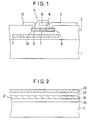
- Figure 1 is a schematic partial sectional view of a semiconductor device for driving a light valve device of a flat plate type.
- the semiconductor device comprises a laminated layer structure 2 formed on a support substrate 1.
- the laminated layer structure 2 includes a light-shielding thin film and a semiconductor thin film formed on the light-shielding thin film via an insulating film as described below.
- a transparent electrode for driving a respective light valve, i.e. a pixel electrode 3 is formed on the surface of the composite substrate including the stacked-layer structure 2. Further, a corresponding switching element 4 is formed in the stacked-layer structure 2 for selectively exciting the pixel electrode 3.
- the switching element 4 has a drain region 5 and a source region 6, both formed in the semiconductor thin film and spaced apart from each other.
- the drain region 5 is connected to a signal line 12 and the source region 6 is connected to the corresponding pixel electrode 3.
- a channel region 7 is provided between the drain region 5 and the source region 6.
- a main gate electrode 9 is formed on the front surface of the channel region 7 via the gate insulating film 8.
- the main gate electrode 9 is connected to a scanning line (not shown) and controls the conductance of the channel region 7 in order to turn the switching element 4 on or off.
- the light-shielding thin film forms a light-shielding layer 11 arranged on the back surface side of the channel region 7 via an insulating layer 10 provided by the insulating film. That is, the light-shielding layer 11 is arranged on the side of the channel region 7 opposite to the main gate electrode 9.
- the light-shielding layer 11 is provided by the aforementioned light-shielding thin film as mentioned above and, in this instance, is electrically conductive so that it also serves as a sub-gate electrode to control back-gating.
- the pair of main and sub-gate electrodes 9 and 11 arranged on both sides of the channel region 7 are made of light-shielding material and, hence, completely prevent light from falling on the channel region 7.
- the channel region 7 is formed of a single silicon crystal semiconductor thin film, to which ordinary LSI processing technogoloy can be directly adapted. Therefore, the channel length can be shortened to the order of submicrons.
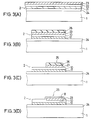
- Figure 2 is a schematic partial sectional view of the composite substrate employed for fabricating the semiconductor device of Figure 1.
- the composite substrate consists of the support substrate 1 and the stacked-layer structure 2 formed thereon as shown.
- the support substrate 1 is composed of a light-transmitting insulating material, such as a heat-resistant quartz consisting chiefly of silicon oxide or aluminium oxide.
- a light-transmitting insulating material such as a heat-resistant quartz consisting chiefly of silicon oxide or aluminium oxide.
- Aluminium oxide exhibits a coefficient of thermal expansion which is close to that of silicon and gives advantages in terms of stress suppresion. Furthermore, since single crystals of aluminium oxide can be formed, it is possible to grow a single crystal semiconductor film hetero-epitaxially thereon.
- the laminated structure 2 adhered to the support substrate 1 has a light-shielding thin film 21 arranged on the support substrate 1, an insulating film 22 arranged on the above light-shielding thin film 21, and a semi-conductor thin film 23, arranged on the insulating film 22 and composed of a single crystal material.
- the light-shielding thin film 21 is composed of an electrically conductive material such as polysilicon.
- a metal film such as a silicide or aluminium instead of the above semiconductor materials.
- aluminium oxide i.e. sapphire
- a single crystal silicon can be hetero-epitaxially grown thereon to form the light-shielding thin film.
- the stacked-layer structure 2 may include a ground film 24 interposed between the support substrate 1 and the light-shielding thin film 21.
- the ground film 24 is provided to improve the adhesion between the support substrate 1 and the stacked-layer structure 2.
- the support substrate 1 is quartz that consists mainly of silicon oxide
- silicon oxide can be used as the ground film 24.
- the ground film 24 should be composed of a layer of silicon nitride or oxynitride, or a multilayer film of at least one of these and silicon oxide.
- oxinitride is advantageous, since it is capable of accommodating stress.
- the insulating film 24 is used as a gate insulating film for the sub-gate electrode, provided by the light-shielding thin film 21, and is composed of, for instance, silicon oxide or silocon nitride.
- the insulating film 22 may be a multilayer film of silicon nitride and silicon oxide.
- the semiconductor thin film 23 positioned on the top of the stacked-layer structure 2 is made, for example, of silicon.
- This silicon may be of a single crystalline form, a polycrystalline form or an amorphous form.
- An amorphous silicon thin film or a polycristalline silicon thin film can easily be deposited on a glass substrate by chemical vapour deposition, and is adaptable to manufacture of an active matrix device having a relatively large screen.
- the active matrix liquid crystal device can have a screen size of about three inches (7.62 cm) to ten inches (25.4 cm).
- the amorphous silicon film can be formed at a temperature as low as 350° or less, and is suitable for liquid crystal panels of large area.
- a polycrystal silicon thin film it is possible to make a small liquid crystal panel of about 2 ⁇ (5.08 cm).
- the switching element has a channel length of the order of microns, a high channel mobility makes it possible to realize a high-speed operation. It is further possible to integrate peripheral circuits for controlling the switching elements on the same support substrate in a large scale and to control the array of switching elements at high speeds, so that the light valve device manufactured using the semiconductor thin film of single crystal silicon is indispensable for displaying very fine moving pictures.
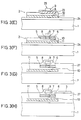
- a composite substrate is prepared as shown in Figure 3(A). That is, the ground film 24 of silicon oxide is formed on the support substrate 1 of polished quartz plate by a chemical vapour deposition method or by sputtering.
- the light-shielding thin film 21 made of polysilicon is deposited on the ground film 24 by a chemical vapour deposition method.
- the insulating film 22 made of silicon oxide is formed on the light-shielding thin film 21 by a thermal oxidation method or by a chemical deposition method.
- the semiconductor thin film 23 of single crystal silicon is formed on the insulating film 22.
- the semiconductor thin film 23 is obtained by adhering a semiconductor substrate of single crystal silicon to the insulating film 22 and then polishing it until its thickness becomes several ⁇ m.
- the single crystal silicon semiconductor substrate to be used is preferably a silicon wafer of high quality that is used for manufacturing LSIs having uniform crystal orientation within a range of [100] 0.0 ⁇ 1.0 and a single crystal lattice defect density of smaller than 500 defects/cm2.
- the surface of the silicon wafer having such physical properties is, first, finished precisely and smoothly.
- the smoothly finished surface is superposed on the insulating film 22 followed by heating to adhere the silicon wafer to the support substrate 1 by thermo-compression bonding.
- the silicon wafer and the support substrate 1 are firmly adhered to each other.
- the silicon wafer is polished until a desired thickness is obtained. It is also possible to carry out an etching process instead of the polishing.
- the thus obtained single crystal silicon semiconductor thin film 23 substantially retains the quality of the silicon wafer, and therefore a semiconductor substrate material is obtained having excellent uniformity in crystal orientation and a low lattice defect density.
- the surface of the silicon wafer that is adhered by thermo-compression bonding has electrical defects to some extent, and the following process is preferred: Si02 is formed in the single crystal wafer by thermal oxidation or chemical vapour deposition. Then, polysilicon is formed by chemical vapour deposition and the surface is polished as required. Thereafter, Si02 is formed by thermal oxidation or chemical vapour deposition, a silicon nitride film is formed by chemical vapour deposition, and Si02 is formed by thermal oxidation or chemical vapour deposition in the order mentioned. The silicon wafer is adhered by thermo-compression bonding onto a quartz support substrate or a quartz support substrate coated with Si02 by chemical vapour deposition and is, then, polished.
- the stacked-layer structure 2, except for the ground film 24, is etched in order to form the light-shielding layer 11 from the light-shielding thin film 21 on the undermost layer, namely, the ground film 24.
- the gate oxide film 10 from the insulating film 22 is formed on the light-shielding layer 11.
- the light-shielding layer 11 is formed by applying a photosensitive film 26 onto the whole surface of the composite substrate followed by patterning it into a desired shape and, then, effecting etching selectively using the patterned photosensitive film 26 as a mask.
- an element region 25 is formed on the two-layer structure consisting of the patterned light-shielding layer 11 and the gate oxide film 10.
- the element region 25 is obtained by selectively etching only the semiconductor thin film 23 into a desired shape.
- the semiconductor thin film 23 is selectively etched by using, as a mask, the photosensitive film 26 that is further patterned to the shape of the element region 25.
- a step shown in Figure 3(D) furthermore, the photosensitive film 26 is removed and, then, a thermally oxidized film is formed on the whole surface inclusive of the surface of the semiconductor thin film 23 that is exposed. As a result, a gate oxide film 8 is formed on the surface of the semiconductor thin film 23.
- a polycrystal silicon film is so deposited by a chemical vapour deposition method as to cover the element region 25.
- the polycrystalline silicon film is selectively etched using a photosensitive film (not shown) that is patterned into a desired shape in order to form the main gate electrode 9.
- the main gate electrode 9 is positioned above the semiconductor thin film 23 via the gate oxide film 8.
- impurity ions are injected through the gate oxide film 8 using the main gate electrode 9 as a mask, in order to form the drain region 5 and the source region 6 in the semiconductor thin film 23.
- transistor channel region 7 that contains no impurity under the main gate electrode 9 between the drain region 5 and the source region 6.
- a protective film 27 is formed so as to cover the element region 25.
- the switching element that includes the light-shielding layer 11 and the main gate electrode 9 is buried under the protective film 27.
- the gate oxide film 8 on the source region 6 is partly removed to form a contact hole, and a transparent pixel electrode 3 is formed so as to cover this portion.
- the pixel electrode 3 is made of a transparent material such as ITO.
- the protective film 27 provided on the lower side of the pixel electrode 3 is made, for example, of silicon oxide and is transparent.
- the support substrate 1 of quartz glass on the lower side thereof is transparent too. Therefore, the three-layer structure consisting of the pixel electorde 3, protective film 27 and quartz glass support substrate 1, is optically transparent and can be utilized for a light valve device of a transmission type.
- the pair of main gate and sub-gate electrodes 9 and 11 that sandwich the channel region 7 vertically are made of polysilicon, which is optically opaque in contrast to the above three-layer structure, and hence they block the entering light and prevent leakage current from flowing into the channel region.
- the incident light can be perfectly blocked by using a material having a low band gap such as silicon, germanium or the like.
- the semiconductor thin film 23 of high-quality single crystal silicon is processed at a temperature higher than 600°C, followed by a photolithoetching technique with high resolution and by ion implantation, making it possible to form an insulated gate field-effect transistor having a size of the order of microns or submicrons.
- a single crystal silicon film of a very high quality is used, and, hence, the obtained insulated gate transistor exhibits excellent electric characteristics.
- the pixel electrode 3 can be formed to a size of the order of microns by miniaturization technology, making it possible to fabricate a semiconductor device for an active matrix liquid crystal panel having a high density and a fine structure.
- FIG 3 shows an embodiment in which the single crystal semiconductor film 23 is formed by thermo-compression bonding.
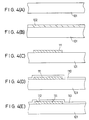
- Figure 4 another embodiment, where the single crystal semiconductor film is formed by an epitaxial method instead of thermo-compression bonding, is illustrated.
- a transparent aluminium oxide substrate 101 such as sapphire
- Figure 4(B) a single crystal silicon film 102 is hetero-epitaxially grown using the crystal of the aluminium oxide 101 as a seed.
- aluminium oxide has a coefficient of thermal expansion that is closer to that of silicon than that of quartz. If polycrystalline aluminium oxide is used as the support substrate of the embodiment shown in Figure 3, the thermal stress is small and the crystallinity of the single crystal silicon film formed thereon can be maintained even after the semiconductor processing at a high temperature.
- Figure 4 showing a process where single crystal aluminium oxide is used, it is possible to grow the single crystal silicon film 102 hetero-epitaxially thereon as shown in Figure 4(B).
- the single crystal silicon film 102 that is grown is patterned as shown in Figure 4(C) to form a light-shielding film 111.
- an insulating film 110 is formed as shown in Figure 4(D), and a hole 112 is made in a portion thereof, so that the surface of the single crystal silicon film 111 is partially exposed as shown in Figure 4(E).
- an amorphous or polycrystalline semiconductor film 123 is formed as shown in Figure 4(F).
- the single crystal silicon crystal film 111 and the semiconductor film 123 are in contact with each other by way of the hole 112. If the heat treatment is carried out in this state at a high temperature, the semiconductor 123 grows laterally and epitaxially with the single crystal silicon film 111 in the hole as a seed. As shown in Figure 4(G), therefore, the region 123A close to the hole is transformed into a single crystal. The region 123B that is not transformed into a single crystal is kept in a polycrystalline form.
- Figure 4(F) illustrates an example in which the polycrystalline semiconductor film 123 is, first, formed and is then grown laterally and epitaxially by a heat treatment
- the single crystal semiconductor film as shown in Figure 4(G) can also be formed by gas-source epitaxy or liquid-phase epitaxy from the state shown in Figure 4(E).
- Use can be made of a silicon film or a GaAs film as a semiconductor film.
- a region 124 that serves as the substrate of a transistor is patterned.
- a gate insulating film 108 is formed and, finally, a transistor is formed in which a transparent electrode 103 is connected with a drain region 106 as shown in Figure 4(J).
- the conductance of a channel region 107 between a source region 105 and the drain region 106 is controlled through a gate electrode 125 and the light-shielding film 111.
- Figure 4(J) illustrates an example in which the light-shielding film 11 is connected to the source region 105, which, however, is not necessary.
- the single crystal region is grown laterally and epitaxially by a length of 3 m to 5 ⁇ m, enabling a single crystal transistor to be formed on the insulating film as shown in Figure 4(J).
- Figure 5 shows an optical valve device that is assembled using the semiconductor device of the present invention.
- the light valve device comprises a semiconductor device 28, a substrate 29 facing the semiconductor device 28, and a layer of an electro-optical material, for example, a liquid crystal layer 30, between the semiconductor device 28 and the facing substrate 29.
- the semiconductor device 28 there are pixel electrodes or drive electrodes 3 that define pixels, and switching elements 4 for activating the drive electrodes 3 in response to predetermined signals.
- the semiconductor device 28 consists of the support substrate 1 composed of quartz glass and the laminated layer structure 2 formed on the support substrate 1. In addition, a polarizer plate 31 is adhered to the back surface of the support substrate 1.
- the switching elements 4 are formed in the single crystal silicon semiconductor thin film included in the stacked-layer structure 2.
- the switching elements 4 are constituted by a plurality of insulated gate field-effect transistors arranged in a matrix. The source region of each transistor is connected to a corresponding pixel electrode 3, the main gate electrode is connected to a scanning line 32, and the drain electrode is connected to a signal line 7.
- the semiconductor device 28 further includes an X-driver 33 connected to the signal lines 7 arranged in columns, and a Y-driver 34 connected to the scanning lines 32 arranged in rows.
- the facing substrate 29 comprises a glass substrate 35, a polarizing plate 36 adhered to the outer surface of the glass substrate 35, and a facing electrode or common electrode 37 formed on the inner surface of the glass substrate 35.
- the light-shielding layer or the sub-gate electrode included in each switching element 4 is preferably connected to the scanning line 32 together with the main electrode.
- the above connection makes it possible effectively to prevent leakage current from flowing into the channel region of the transistor that constitutes the switching element.
- the light-shielding layer can be connected to the source region or the drain region of the corresponding transistor.
- a predetermined voltage is applied to the light-shielding layer to effectively prevent leakage current from flowing due to the back gating.
- the threshold voltage of the channel region can be set to a desired value.
- each switching element 4 is connected in common to the scanning line 32, and are supplied with scanning signals from the Y-driver 34. Therefore, the turn-on/off of the switching elements 4 is controlled line by line.
- a data signal output from the X-driver 33 is applied, via the signal line 7, to a selected switching element 4 that has been turned on.
- the applied data signal is transmitted to the corresponding pixel electrode 3 to excite it and acts upon the liquid crystal layer 30, so that its transmission factor becomes substantially 100%.
- the switching element 4 is left non-conductive and maintains the data signal written on the pixel electrode as electric charge.
- the liquid crystal layer 30 has a large resistivity and usually operates a capacitive element.
- An on/off current ratio is used to represent the switching performance of the switching elements 4.
- the current ratio necessary for operating the liquid crystal can easily be found from the write time and the holding time. For instance, when the data signal is a televison signal, more than 90% of the data signal must be written within about 60 ⁇ sec of one scanning period. On the other hand, more than 90% of the electric charge must be retained for a period of one field, which is about 16 msec. Therefore, the current ratio must be at least of the order of ten thousand.
- the conductance of the channel region is controlled from both surfaces thereof by the main gate and sub-gate electrodes, and the leakage current is substantially wholly eliminated during the off period.
- the on/off ratio of the switching elements having such a structure is of the order of a hundred thousand or greater. It is, therefore, possible to obtain a light valve device of an active matrix type having a very fast signal response characteristic.
- a pair of main gate and sub-gate electrodes arranged on both sides of the transistor channel region are formed using a light-shielding material, such as polysilicon, whereby light is effectively blocked from entering the channel region from outside, making it possible effectively to prevent the occurrence of leakage current by the photo-electric effect.
- a light-shielding material such as polysilicon
- a semiconductor device for driving light valves of a flat plate type can be obtained, which features very high response characteristics and is free from erroneous operation.
- the switching elements consisting of insulated gate field-effect transistors in the semiconductor thin film of single crystal silicon, it is possible to obtain a flat-type semiconductor device for driving light valves that has a very fine and very large scale integration structure.
Abstract
Description
- The present invention relates to light valve devices of a flat plate type, such as active matrix liquid crystal panels for displays of a direct viewing type or of a projection type. More specifically, the invention relates to a semiconductor device for providing a substrate of such a liquid crystal panel.
- An active matrix device is based on a simple principle, in which each pixel is equipped with a switching element and, when a particular pixel is selected, the corresponding switching element is made to be conductive and, when it is not selected, the switching element is made to be non-conductive. The switching elements are formed on a glass substrate which forms part of the device. Therefore, the technology for miniaturising the switching elements and making them thin is very important. Thin film transistors are ordinarily used as such switching elements.
- In a conventional active matrix device, a thin film transistor has so far been formed on a thin silicon film that is deposited on the glass substrate. Such transistors are generally of an insulated gate field effect type. A transistor of this type has a channel region formed in the thin silicon film and a gate electrode formed so as to cover the channel region. A predetermined voltage is applied to the gate electrode to control the conductance of the channel region and to carry out the switching operation.
- The conventional insulated gate-type thin film transistors have a problem in that a leakage current may flow into the channel region through the back side of the thin film even when the channel region is made non-conductive by controlling the gate voltage. That is, so-called "back channel" or "backgating" takes place impairing the proper operation of the active matrix device. In order to operate the pixels at high speeds by a line sequence system, the conductance ratio of the switching elements, between the conductive state and the non-conductive state, must be greater than 10⁶ . In fact, however, the back-gating makes it difficult to obtain the required switching performance.
- Even if the back-gating were eliminated, the channel region of the thin-film transistor tends to exhibit an increased conductance if light from an external source falls thereon, the semiconductor device being used under an illuminated condition, and this causes leakage current in the drain and source in the non-conductive state. Further, the ratio of this leakage current to the leakage current when no light enters increases with an increase in the quality of the semiconductor thin film, such as a single crystal film, that forms the channel regions, causing another problem.
- In view of the above-mentioned problems, it is an object of the present invention at least in its preferred form to provide a semiconductor device for driving light valves of a flat plate type, which has thin film transistors with a structure capable of effectively preventing back-gating and of blocking incident light.
- In accordance with the first aspect of the present invention there is provided a semiconductor device for use in a light valve device, comprising a support substrate; a semiconductor thin film on the support substrate; a switching transistor having a channel region formed in the semiconductor thin film and a main gate electrode for controlling the channel region; and an electrode electrically connected to the switching transistor for energisation by the switching transistor; characterised in that a leakage current inhibiting layer is disposed on the side of the channel region opposite the main gate electrode.
- A semiconductor according to the present invention comprises a substrate having a stacked structure, which includes an insulating support substrate made of a light-transmitting material, a light-shielding thin film provided on the support substrate, and a semiconductor thin film provided on the light-shielding thin film via an insulating film. Transparent electrodes for driving light valves, i.e. pixel electrodes, are arranged on the support substrate. Furthermore, switching elements are provided for selectively exciting the pixel electrodes. Each of the switching elements comprises an insulated gate field effect transistor having a channel region and main gate electrode for controlling the channel region. A channel region is formed in the semiconductor thin film, and the main gate electrode is formed so as to cover the channel region. The light-shielding thin film is provided on the side of the channel region opposite the main gate electrode so that the channel region is sandwiched between the main gate electrode and the light-shielding thin film in the vertical direction.
- Preferably, the main gate electrode is also made of a light-shielding material and together with the light-shielding thin film substantially entirely blocks light from reaching the channel region from the outside.
- Advantageously, the light-shielding thin film is made of an electrically conductive material to eliminate back-gating. The light-shielding thin film may serve as a sub-gate electrode, and may be arranged to receive an electric current in order to control back-gating.
- If the semi-conductor thin film is a single crystal silicon thin film, the channel region can be precisely fabricated to within the order of sub-microns using ordinary LSI technology.
- In the preferred embodiment described below, the conductance of the channel region of each of a plurality of transistors is controlled by main gate and sub-gate electrodes provided on both sides of the semi-conductor thin film via insulating films. Therefore, no back-gating develops, by contrast with the conventional construction, in which a single gate electrode is provided on only one surface of the channel region of a thin film transistor. In other words, the sub-gate electrodes serve to suppress the back-gating.
- In addition, since in the preferred embodiment the channel region of each transistor is covered by a couple of light-shielding gate electrodes from both the upper and the lower sides, light incident on the device passes through the electrode but is nearly completely blocked from the channel region, rendering it possible effectively to prevent the generation of photoelectric current.
- According to a further aspect of the present invention, there is provided a method of fabricating a semiconductor device characterised by steps of forming a substrate by laminating a light-shielding thin layer, an insulating film and a semiconductor thin film on a support substrate; forming a light-shielding layer pattern by selectively etching said laminated layers; forming a switching transistor having a channel region in said semiconductor thin film and a main gate electrode covering said channel region; and forming an electrode electrically connected to the switching element on said substrate.
- The invention is described further, by way of example, with reference to the accompanying drawings, in which:-
- Figure 1 is partial sectional view through a flat-type semiconductor device according to the invention for driving a light valve device;
- Figure 2 is a partial sectional view through a composite substrate employed for fabricating the semiconductor device of Figure 1;
- Figures 3(A) to 3(H) are schematic diagrams illustrating different steps in the fabrication of the semiconductor device of Figure 1;
- Figures 4(A) to 4(J) are schematic diagrams illustrating different steps in the fabrication of a further semi-conductor device according to the invention; and
- Figure 5 is a perspective exploded view, which schematically illustrates the structure of a light valve device of a flat plate type incorporating the semiconductor device according to the invention.
- Figure 1 is a schematic partial sectional view of a semiconductor device for driving a light valve device of a flat plate type. The semiconductor device comprises a laminated
layer structure 2 formed on asupport substrate 1. The laminatedlayer structure 2 includes a light-shielding thin film and a semiconductor thin film formed on the light-shielding thin film via an insulating film as described below. A transparent electrode for driving a respective light valve, i.e. apixel electrode 3, is formed on the surface of the composite substrate including the stacked-layer structure 2. Further, acorresponding switching element 4 is formed in the stacked-layer structure 2 for selectively exciting thepixel electrode 3. - The switching
element 4 has adrain region 5 and asource region 6, both formed in the semiconductor thin film and spaced apart from each other. Thedrain region 5 is connected to asignal line 12 and thesource region 6 is connected to thecorresponding pixel electrode 3. Moreover, achannel region 7 is provided between thedrain region 5 and thesource region 6. Amain gate electrode 9 is formed on the front surface of thechannel region 7 via the gateinsulating film 8. Themain gate electrode 9 is connected to a scanning line (not shown) and controls the conductance of thechannel region 7 in order to turn theswitching element 4 on or off. - The light-shielding thin film forms a light-
shielding layer 11 arranged on the back surface side of thechannel region 7 via aninsulating layer 10 provided by the insulating film. That is, the light-shielding layer 11 is arranged on the side of thechannel region 7 opposite to themain gate electrode 9. The light-shielding layer 11 is provided by the aforementioned light-shielding thin film as mentioned above and, in this instance, is electrically conductive so that it also serves as a sub-gate electrode to control back-gating. - The pair of main and
sub-gate electrodes channel region 7 are made of light-shielding material and, hence, completely prevent light from falling on thechannel region 7. - In this embodiment, furthermore the
channel region 7 is formed of a single silicon crystal semiconductor thin film, to which ordinary LSI processing technogoloy can be directly adapted. Therefore, the channel length can be shortened to the order of submicrons. - Figure 2 is a schematic partial sectional view of the composite substrate employed for fabricating the semiconductor device of Figure 1. The composite substrate consists of the
support substrate 1 and the stacked-layer structure 2 formed thereon as shown. - First, the
support substrate 1 is composed of a light-transmitting insulating material, such as a heat-resistant quartz consisting chiefly of silicon oxide or aluminium oxide. Aluminium oxide exhibits a coefficient of thermal expansion which is close to that of silicon and gives advantages in terms of stress suppresion. Furthermore, since single crystals of aluminium oxide can be formed, it is possible to grow a single crystal semiconductor film hetero-epitaxially thereon. - Next, the laminated
structure 2 adhered to thesupport substrate 1 has a light-shieldingthin film 21 arranged on thesupport substrate 1, aninsulating film 22 arranged on the above light-shieldingthin film 21, and a semi-conductorthin film 23, arranged on theinsulating film 22 and composed of a single crystal material. The light-shieldingthin film 21 is composed of an electrically conductive material such as polysilicon. Alternatively, it is possible to use a single layer film of germanium, silicon-germanium or silicon, or a multi-layer film of silicon including at least one layer of germanium or silicon-germanium, instead of the single layer film of polysilicon. It is further possible to use a metal film such as a silicide or aluminium instead of the above semiconductor materials. When aluminium oxide, i.e. sapphire, is used as the support substrate, furthermore a single crystal silicon can be hetero-epitaxially grown thereon to form the light-shielding thin film. - The stacked-
layer structure 2 may include aground film 24 interposed between thesupport substrate 1 and the light-shieldingthin film 21. Theground film 24 is provided to improve the adhesion between thesupport substrate 1 and the stacked-layer structure 2. For instance, when thesupport substrate 1 is quartz that consists mainly of silicon oxide, silicon oxide can be used as theground film 24. When it is desirable for theground film 24 to block the infiltration of impurities from thesupport substrate 1, furthermore, the ground film should be composed of a layer of silicon nitride or oxynitride, or a multilayer film of at least one of these and silicon oxide. In particular, oxinitride is advantageous, since it is capable of accommodating stress. - The insulating
film 24 is used as a gate insulating film for the sub-gate electrode, provided by the light-shieldingthin film 21, and is composed of, for instance, silicon oxide or silocon nitride. Alternatively, the insulatingfilm 22 may be a multilayer film of silicon nitride and silicon oxide. - The semiconductor
thin film 23 positioned on the top of the stacked-layer structure 2 is made, for example, of silicon. This silicon may be of a single crystalline form, a polycrystalline form or an amorphous form. An amorphous silicon thin film or a polycristalline silicon thin film can easily be deposited on a glass substrate by chemical vapour deposition, and is adaptable to manufacture of an active matrix device having a relatively large screen. When such an armorphous silicon thin film is used, the active matrix liquid crystal device can have a screen size of about three inches (7.62 cm) to ten inches (25.4 cm). In particular, the amorphous silicon film can be formed at a temperature as low as 350° or less, and is suitable for liquid crystal panels of large area. When a polycrystal silicon thin film is used, it is possible to make a small liquid crystal panel of about 2˝ (5.08 cm). - In the case of a polycrystal silicon thin film, however, the reproducibility of constant elements is poor and variations increase when a transistor having a channel length of the order of submicrons is formed by fine semiconductor processing technology. When amorphous silicon is used, further, high-speed switching cannot be realized even though the submicron processing technology is employed. When a semiconductor thin film of single crystal silicon is used, on the other hand, it is possible to employ fine semiconductor processing technology greatly to increase the density of switching elements and to obtain an ultra-fine light valve device.
- Even though the switching element has a channel length of the order of microns, a high channel mobility makes it possible to realize a high-speed operation. It is further possible to integrate peripheral circuits for controlling the switching elements on the same support substrate in a large scale and to control the array of switching elements at high speeds, so that the light valve device manufactured using the semiconductor thin film of single crystal silicon is indispensable for displaying very fine moving pictures.
- A method of fabricating the semiconductor device according to the present invention is described below in detail with reference to Figure 3. First, a composite substrate is prepared as shown in Figure 3(A). That is, the
ground film 24 of silicon oxide is formed on thesupport substrate 1 of polished quartz plate by a chemical vapour deposition method or by sputtering. The light-shieldingthin film 21 made of polysilicon is deposited on theground film 24 by a chemical vapour deposition method. Then, the insulatingfilm 22 made of silicon oxide is formed on the light-shieldingthin film 21 by a thermal oxidation method or by a chemical deposition method. Lastly, the semiconductorthin film 23 of single crystal silicon is formed on the insulatingfilm 22. - The semiconductor
thin film 23 is obtained by adhering a semiconductor substrate of single crystal silicon to the insulatingfilm 22 and then polishing it until its thickness becomes several µm. The single crystal silicon semiconductor substrate to be used is preferably a silicon wafer of high quality that is used for manufacturing LSIs having uniform crystal orientation within a range of [100] 0.0 ± 1.0 and a single crystal lattice defect density of smaller than 500 defects/cm². The surface of the silicon wafer having such physical properties is, first, finished precisely and smoothly. - Then, the smoothly finished surface is superposed on the insulating
film 22 followed by heating to adhere the silicon wafer to thesupport substrate 1 by thermo-compression bonding. By means of the thermo-compression bonding, the silicon wafer and thesupport substrate 1 are firmly adhered to each other. In this state, the silicon wafer is polished until a desired thickness is obtained. It is also possible to carry out an etching process instead of the polishing. The thus obtained single crystal silicon semiconductorthin film 23 substantially retains the quality of the silicon wafer, and therefore a semiconductor substrate material is obtained having excellent uniformity in crystal orientation and a low lattice defect density. - With current technologies, the surface of the silicon wafer that is adhered by thermo-compression bonding has electrical defects to some extent, and the following process is preferred: Si0₂ is formed in the single crystal wafer by thermal oxidation or chemical vapour deposition. Then, polysilicon is formed by chemical vapour deposition and the surface is polished as required. Thereafter, Si0₂ is formed by thermal oxidation or chemical vapour deposition, a silicon nitride film is formed by chemical vapour deposition, and Si0₂ is formed by thermal oxidation or chemical vapour deposition in the order mentioned. The silicon wafer is adhered by thermo-compression bonding onto a quartz support substrate or a quartz support substrate coated with Si0₂ by chemical vapour deposition and is, then, polished.
- Next, in a step shown in Figure 3(B), the stacked-
layer structure 2, except for theground film 24, is etched in order to form the light-shielding layer 11 from the light-shieldingthin film 21 on the undermost layer, namely, theground film 24. At the same time, thegate oxide film 10 from the insulatingfilm 22 is formed on the light-shielding layer 11. The light-shielding layer 11 is formed by applying aphotosensitive film 26 onto the whole surface of the composite substrate followed by patterning it into a desired shape and, then, effecting etching selectively using the patternedphotosensitive film 26 as a mask. - Then, in a step shown in Figure 3(C), an
element region 25 is formed on the two-layer structure consisting of the patterned light-shielding layer 11 and thegate oxide film 10. Theelement region 25 is obtained by selectively etching only the semiconductorthin film 23 into a desired shape. The semiconductorthin film 23 is selectively etched by using, as a mask, thephotosensitive film 26 that is further patterned to the shape of theelement region 25. - In a step shown in Figure 3(D), furthermore, the
photosensitive film 26 is removed and, then, a thermally oxidized film is formed on the whole surface inclusive of the surface of the semiconductorthin film 23 that is exposed. As a result, agate oxide film 8 is formed on the surface of the semiconductorthin film 23. - Then, in a step shown in Figure 3(E), a polycrystal silicon film is so deposited by a chemical vapour deposition method as to cover the
element region 25. The polycrystalline silicon film is selectively etched using a photosensitive film (not shown) that is patterned into a desired shape in order to form themain gate electrode 9. Themain gate electrode 9 is positioned above the semiconductorthin film 23 via thegate oxide film 8. - In a step shown in Figure 3(F), impurity ions are injected through the
gate oxide film 8 using themain gate electrode 9 as a mask, in order to form thedrain region 5 and thesource region 6 in the semiconductorthin film 23. As a result, there is formed atransistor channel region 7 that contains no impurity under themain gate electrode 9 between thedrain region 5 and thesource region 6. - Next, in a step shown in Figure 3(G), a
protective film 27 is formed so as to cover theelement region 25. As a result, the switching element that includes the light-shielding layer 11 and themain gate electrode 9 is buried under theprotective film 27. - Lastly, in a step shown in Figure 3(H), the
gate oxide film 8 on thesource region 6 is partly removed to form a contact hole, and atransparent pixel electrode 3 is formed so as to cover this portion. Thepixel electrode 3 is made of a transparent material such as ITO. In addition, theprotective film 27 provided on the lower side of thepixel electrode 3 is made, for example, of silicon oxide and is transparent. Moreover,thesupport substrate 1 of quartz glass on the lower side thereof is transparent too. Therefore, the three-layer structure consisting of thepixel electorde 3,protective film 27 and quartzglass support substrate 1, is optically transparent and can be utilized for a light valve device of a transmission type. - The pair of main gate and
sub-gate electrodes channel region 7 vertically are made of polysilicon, which is optically opaque in contrast to the above three-layer structure, and hence they block the entering light and prevent leakage current from flowing into the channel region. The incident light can be perfectly blocked by using a material having a low band gap such as silicon, germanium or the like. - In the manufacturing method shown in Figure 3 as described above, the semiconductor
thin film 23 of high-quality single crystal silicon is processed at a temperature higher than 600°C, followed by a photolithoetching technique with high resolution and by ion implantation, making it possible to form an insulated gate field-effect transistor having a size of the order of microns or submicrons. A single crystal silicon film of a very high quality is used, and, hence, the obtained insulated gate transistor exhibits excellent electric characteristics. At the same time, thepixel electrode 3 can be formed to a size of the order of microns by miniaturization technology, making it possible to fabricate a semiconductor device for an active matrix liquid crystal panel having a high density and a fine structure. - Figure 3 shows an embodiment in which the single
crystal semiconductor film 23 is formed by thermo-compression bonding. Referring to Figure 4, another embodiment, where the single crystal semiconductor film is formed by an epitaxial method instead of thermo-compression bonding, is illustrated. First, a transparentaluminium oxide substrate 101, such as sapphire, is used as the support substrate as shown in Figure 4(A). Next, as shown in Figure 4(B), a singlecrystal silicon film 102 is hetero-epitaxially grown using the crystal of thealuminium oxide 101 as a seed. - In the polycrystalline form, aluminium oxide has a coefficient of thermal expansion that is closer to that of silicon than that of quartz. If polycrystalline aluminium oxide is used as the support substrate of the embodiment shown in Figure 3, the thermal stress is small and the crystallinity of the single crystal silicon film formed thereon can be maintained even after the semiconductor processing at a high temperature. In Figure 4 showing a process where single crystal aluminium oxide is used, it is possible to grow the single
crystal silicon film 102 hetero-epitaxially thereon as shown in Figure 4(B). - Next, the single
crystal silicon film 102 that is grown is patterned as shown in Figure 4(C) to form a light-shieldingfilm 111. Then, an insulatingfilm 110 is formed as shown in Figure 4(D), and ahole 112 is made in a portion thereof, so that the surface of the singlecrystal silicon film 111 is partially exposed as shown in Figure 4(E). Next, an amorphous orpolycrystalline semiconductor film 123 is formed as shown in Figure 4(F). - The single crystal
silicon crystal film 111 and thesemiconductor film 123 are in contact with each other by way of thehole 112. If the heat treatment is carried out in this state at a high temperature, thesemiconductor 123 grows laterally and epitaxially with the singlecrystal silicon film 111 in the hole as a seed. As shown in Figure 4(G), therefore, theregion 123A close to the hole is transformed into a single crystal. Theregion 123B that is not transformed into a single crystal is kept in a polycrystalline form. - Although Figure 4(F) illustrates an example in which the
polycrystalline semiconductor film 123 is, first, formed and is then grown laterally and epitaxially by a heat treatment, it should be noted that the single crystal semiconductor film, as shown in Figure 4(G), can also be formed by gas-source epitaxy or liquid-phase epitaxy from the state shown in Figure 4(E). Use can be made of a silicon film or a GaAs film as a semiconductor film. - Next, as shown in Figure 4(H), a
region 124 that serves as the substrate of a transistor is patterned. Next, as shown in Figure 4(I), agate insulating film 108 is formed and, finally, a transistor is formed in which atransparent electrode 103 is connected with adrain region 106 as shown in Figure 4(J). The conductance of achannel region 107 between asource region 105 and thedrain region 106 is controlled through agate electrode 125 and the light-shieldingfilm 111. Figure 4(J) illustrates an example in which the light-shieldingfilm 11 is connected to thesource region 105, which, however, is not necessary. In Figure 4(G), the single crystal region is grown laterally and epitaxially by a length of 3 m to 5 µm, enabling a single crystal transistor to be formed on the insulating film as shown in Figure 4(J). - Figure 5 shows an optical valve device that is assembled using the semiconductor device of the present invention. As shown, the light valve device comprises a
semiconductor device 28, asubstrate 29 facing thesemiconductor device 28, and a layer of an electro-optical material, for example, aliquid crystal layer 30, between thesemiconductor device 28 and the facingsubstrate 29. In thesemiconductor device 28, there are pixel electrodes or driveelectrodes 3 that define pixels, and switchingelements 4 for activating thedrive electrodes 3 in response to predetermined signals. - The
semiconductor device 28 consists of thesupport substrate 1 composed of quartz glass and thelaminated layer structure 2 formed on thesupport substrate 1. In addition, apolarizer plate 31 is adhered to the back surface of thesupport substrate 1. Theswitching elements 4 are formed in the single crystal silicon semiconductor thin film included in the stacked-layer structure 2. Theswitching elements 4 are constituted by a plurality of insulated gate field-effect transistors arranged in a matrix. The source region of each transistor is connected to acorresponding pixel electrode 3, the main gate electrode is connected to ascanning line 32, and the drain electrode is connected to asignal line 7. - The
semiconductor device 28 further includes an X-driver 33 connected to thesignal lines 7 arranged in columns, and a Y-driver 34 connected to thescanning lines 32 arranged in rows. The facingsubstrate 29 comprises aglass substrate 35, apolarizing plate 36 adhered to the outer surface of theglass substrate 35, and a facing electrode orcommon electrode 37 formed on the inner surface of theglass substrate 35. - Although not illustrated, the light-shielding layer or the sub-gate electrode included in each switching
element 4 is preferably connected to thescanning line 32 together with the main electrode. The above connection makes it possible effectively to prevent leakage current from flowing into the channel region of the transistor that constitutes the switching element. Or, the light-shielding layer can be connected to the source region or the drain region of the corresponding transistor. In any event, a predetermined voltage is applied to the light-shielding layer to effectively prevent leakage current from flowing due to the back gating. By controlling the voltage applied to the light-shielding layer, furthermore, the threshold voltage of the channel region can be set to a desired value. - Operation of the light valve device will now be described in detail with reference to Figure 5. The main gate and sub-gate electrodes of each switching
element 4 are connected in common to thescanning line 32, and are supplied with scanning signals from the Y-driver 34. Therefore, the turn-on/off of theswitching elements 4 is controlled line by line. A data signal output from the X-driver 33 is applied, via thesignal line 7, to a selected switchingelement 4 that has been turned on. The applied data signal is transmitted to thecorresponding pixel electrode 3 to excite it and acts upon theliquid crystal layer 30, so that its transmission factor becomes substantially 100%. When not selected, on the other hand, the switchingelement 4 is left non-conductive and maintains the data signal written on the pixel electrode as electric charge. Here, theliquid crystal layer 30 has a large resistivity and usually operates a capacitive element. - An on/off current ratio is used to represent the switching performance of the
switching elements 4. The current ratio necessary for operating the liquid crystal can easily be found from the write time and the holding time. For instance, when the data signal is a televison signal, more than 90% of the data signal must be written within about 60 µsec of one scanning period. On the other hand, more than 90% of the electric charge must be retained for a period of one field, which is about 16 msec. Therefore, the current ratio must be at least of the order of ten thousand. In this respect, according to the present invention, the conductance of the channel region is controlled from both surfaces thereof by the main gate and sub-gate electrodes, and the leakage current is substantially wholly eliminated during the off period. The on/off ratio of the switching elements having such a structure is of the order of a hundred thousand or greater. It is, therefore, possible to obtain a light valve device of an active matrix type having a very fast signal response characteristic. - According to the present invention as described above, a pair of main gate and sub-gate electrodes arranged on both sides of the transistor channel region are formed using a light-shielding material, such as polysilicon, whereby light is effectively blocked from entering the channel region from outside, making it possible effectively to prevent the occurrence of leakage current by the photo-electric effect. Moreover, since the transistor channel region formed in the semiconductor thin film is controlled from the upper and lower sides thereof by the main gate electrode and by the light-shielding layer composed of an electrically conductive material, i.e. by the sub-gate electrode, so-called back gating is effectively prevented, and a thin-film transistor having an excellent on/off ratio is obtained. As a result, a semiconductor device for driving light valves of a flat plate type can be obtained, which features very high response characteristics and is free from erroneous operation. In addition, by forming the switching elements consisting of insulated gate field-effect transistors in the semiconductor thin film of single crystal silicon, it is possible to obtain a flat-type semiconductor device for driving light valves that has a very fine and very large scale integration structure.
Claims (14)
- A semiconductor device for use in a light valve device, comprising a support substrate (1); a semiconductor thin film (23) on the support substrate; a switching transistor (4) having a channel region (7) formed in the semiconductor thin film and a main gate electrode (9) for controlling the channel region; and an electrode (3) electrically connected to the switching transistor for energisation by the switching transistor; characterised in that a leakage current inhibiting layer (11) is disposed on the side of the channel region opposite the main gate electrode.
- A semiconductor device according to claim 1 characerised in that the leakage current inhibiting layer is made of an electrically conductive material.
- A semiconductor device according to claim 1 or 2 characterised in that the leakage current inhibiting layer comprises a light-shielding thin film.
- A semiconductor device according to claim 3 characterised in that the light shielding thin film is made of polysilicon.
- A semiconductor device according to claim 3 characterised in that the light-shielding thin film is made of single crystal silicon that is hetero-epitaxially grown on the support substrate.
- A semiconductor device according to claim 3 characterised in that the light-shielding thin film comprises a single layer film or a multi-layer film and includes at least one of germanium, silicon-germanium, and silicon.
- A semiconductor device according to any of claims 3 to 6 claim characterised in that the light-shielding thin film is disposed between the support substrate and the channel region and is separated from the channel region by an insulating film (10).
- A semiconductor device according to claim 7 characterised in that the insulating film includes at least one of silicon nitride and silicon oxide.
- A semiconductor device according to any of claims 3 to 8 characterised in that the light-shielding thin film is disposed on a ground film (24) on the support substrate, and in that the ground film is made of oxynitride or silicon oxide.
- A semiconductor device according to any preceding claim characterised in that the semiconductor thin film is a single crystal silicon thin film.
- A method of fabricating a semiconductor device characterised by the steps of forming a substrate (1,2) by laminating a light-shielding thin layer (21), an insulating film (22) and a semiconductor thin film (23) on a support substrate (1); forming a light-shielding layer pattern by selectively etching said laminated layers; forming a switching transistor (4) having a channel region (7) in said semiconductor thin film and a main gate electrode (9) covering said channel region; and forming an electrode (3) electrically connected to the switching element on said substrate.
- A semiconductor device characterised by a composite substrate (1,2) having a stacked layer structure comprising a support substrate (1), a light-shielding thin film (11) provided on said support substrate, an insulating film (10) provided at least on said light-shielding thin film, and a semiconductor thin film (5,6,7) disposed on said insulating film; a transparent electrode (3) formed on a portion of said composite substrate where at least said light-shielding thin film is removed; and a switching element (4), connected electrically to said transparent electrode, consisting of a transistor including a channel region (7) formed in said semiconductor thin film and a main gate electrode (9) for controlling the conduction in said channel region, wherein the light-shielding thin film layer is disposed on the side opposite the said main gate electrode with respect to said channel region.
- A composite substrate having a stacked layer structure characterised by a support substrate (1) made of a light-transmitting insulating layer, a light-shielding thin film (11) formed on said support substrate, an insulating film (10) formed at least over said light-shielding thin film, and a semiconductor thin film (23), which is made of single crystalline material, fixedly laminated on said insulating film.
- A light valve device characterised by a composite substrate having stacked layers including a support substrate (1), a light-shielding thin film (11) formed on said support substrate, an insulating film (10) formed at least over said light-shielding thin film, a semi-conducting film (5,6,7) disposed on said insulating film, a pixel electrode (3) formed on said semiconductor film and a switching element (4) formed on said semiconductor film for energising said pixel electrode; an opposed substrate (29) opposite to said composite substrate at a predetermined gap; and an electro-optical material (30) filling up said gap for optically changing in accordance with energisation of said pixel electrode.
Applications Claiming Priority (3)
| Application Number | Priority Date | Filing Date | Title |
|---|---|---|---|
| JP277436/90 | 1990-10-16 | ||
| JP27743690 | 1990-10-16 | ||
| JP27743690A JPH0824193B2 (en) | 1990-10-16 | 1990-10-16 | Manufacturing method of semiconductor device for driving flat plate type light valve |
Publications (3)
| Publication Number | Publication Date |
|---|---|
| EP0481734A2 true EP0481734A2 (en) | 1992-04-22 |
| EP0481734A3 EP0481734A3 (en) | 1993-08-25 |
| EP0481734B1 EP0481734B1 (en) | 1999-12-29 |
Family
ID=17583540
Family Applications (1)
| Application Number | Title | Priority Date | Filing Date |
|---|---|---|---|
| EP91309495A Expired - Lifetime EP0481734B1 (en) | 1990-10-16 | 1991-10-15 | Light valve device |
Country Status (5)
| Country | Link |
|---|---|
| US (6) | US5233211A (en) |
| EP (1) | EP0481734B1 (en) |
| JP (1) | JPH0824193B2 (en) |
| KR (1) | KR100238640B1 (en) |
| DE (1) | DE69131879T2 (en) |
Cited By (11)
| Publication number | Priority date | Publication date | Assignee | Title |
|---|---|---|---|---|
| EP0853254A2 (en) * | 1992-09-11 | 1998-07-15 | Kopin Corporation | Liquid crystal display |
| EP0862077A2 (en) * | 1997-02-27 | 1998-09-02 | Seiko Epson Corporation | Liquid crystal device, manufacturing method thereof and projection type display device |
| EP0991126A1 (en) * | 1997-12-09 | 2000-04-05 | Seiko Epson Corporation | Method of manufacturing semiconductor device and semiconductor device, method of manufacturing electrooptic device and electrooptic device, and electronic apparatus employing it |
| EP0997769A2 (en) * | 1998-10-28 | 2000-05-03 | Sony Corporation | Active matrix liquid crystal display device |
| US6313012B1 (en) * | 1993-09-06 | 2001-11-06 | Hitachi, Ltd. | Method of fabricating multi-layered structure having single crystalline semiconductor film formed on insulator |
| EP1209748A1 (en) * | 2000-11-15 | 2002-05-29 | Matsushita Electric Industrial Co., Ltd. | TFT display matrix having pixel electrodes formed simultaneously with the TFT channel |
| US6511187B1 (en) | 1992-02-20 | 2003-01-28 | Kopin Corporation | Method of fabricating a matrix display system |
| US7501685B2 (en) | 1999-08-31 | 2009-03-10 | Semiconductor Energy Laboratory Co., Ltd. | Display device comprising pixel portion |
| US7541618B2 (en) | 1999-09-27 | 2009-06-02 | Semiconductor Energy Laboratory Co., Ltd. | Liquid crystal device having a thin film transistor |
| CN100557491C (en) * | 1992-06-09 | 2009-11-04 | 株式会社半导体能源研究所 | Semiconductor devices |
| CN100559246C (en) * | 1992-05-29 | 2009-11-11 | 株式会社半导体能源研究所 | Active matrix liquid crystal display apparatus |
Families Citing this family (85)
| Publication number | Priority date | Publication date | Assignee | Title |
|---|---|---|---|---|
| JPH0824193B2 (en) * | 1990-10-16 | 1996-03-06 | 工業技術院長 | Manufacturing method of semiconductor device for driving flat plate type light valve |
| US5347154A (en) * | 1990-11-15 | 1994-09-13 | Seiko Instruments Inc. | Light valve device using semiconductive composite substrate |
| US5499124A (en) | 1990-12-31 | 1996-03-12 | Vu; Duy-Phach | Polysilicon transistors formed on an insulation layer which is adjacent to a liquid crystal material |
| US5475514A (en) * | 1990-12-31 | 1995-12-12 | Kopin Corporation | Transferred single crystal arrayed devices including a light shield for projection displays |
| US6627953B1 (en) | 1990-12-31 | 2003-09-30 | Kopin Corporation | High density electronic circuit modules |
| US5256562A (en) * | 1990-12-31 | 1993-10-26 | Kopin Corporation | Method for manufacturing a semiconductor device using a circuit transfer film |
| US6143582A (en) | 1990-12-31 | 2000-11-07 | Kopin Corporation | High density electronic circuit modules |
| US6593978B2 (en) * | 1990-12-31 | 2003-07-15 | Kopin Corporation | Method for manufacturing active matrix liquid crystal displays |
| JP3092761B2 (en) * | 1991-12-02 | 2000-09-25 | キヤノン株式会社 | Image display device and method of manufacturing the same |
| US5317433A (en) * | 1991-12-02 | 1994-05-31 | Canon Kabushiki Kaisha | Image display device with a transistor on one side of insulating layer and liquid crystal on the other side |
| JP2821830B2 (en) * | 1992-05-14 | 1998-11-05 | セイコーインスツルメンツ株式会社 | Semiconductor thin film device and its application device and method of manufacturing semiconductor thin film device |
| US5923071A (en) * | 1992-06-12 | 1999-07-13 | Seiko Instruments Inc. | Semiconductor device having a semiconductor film of low oxygen concentration |
| KR0131062B1 (en) * | 1992-08-27 | 1998-04-14 | 순페이 야마자끼 | Fabrication method for film-like semiconductor device |
| KR100268007B1 (en) * | 1992-12-22 | 2000-10-16 | 구본준 | Fabrication method of lcd |
| US5982002A (en) * | 1993-01-27 | 1999-11-09 | Seiko Instruments Inc. | Light valve having a semiconductor film and a fabrication process thereof |
| KR100294026B1 (en) * | 1993-06-24 | 2001-09-17 | 야마자끼 순페이 | Electro-optical device |
| JP3644980B2 (en) * | 1993-09-06 | 2005-05-11 | 株式会社ルネサステクノロジ | Manufacturing method of semiconductor device |
| US7081938B1 (en) | 1993-12-03 | 2006-07-25 | Semiconductor Energy Laboratory Co., Ltd. | Electro-optical device and method for manufacturing the same |
| JPH07159974A (en) * | 1993-12-09 | 1995-06-23 | Ryoden Semiconductor Syst Eng Kk | Pattern transfer mask and its production |
| JPH07302912A (en) | 1994-04-29 | 1995-11-14 | Semiconductor Energy Lab Co Ltd | Semiconductor device |
| JP2900229B2 (en) * | 1994-12-27 | 1999-06-02 | 株式会社半導体エネルギー研究所 | Semiconductor device, manufacturing method thereof, and electro-optical device |
| JP3364081B2 (en) * | 1995-02-16 | 2003-01-08 | 株式会社半導体エネルギー研究所 | Method for manufacturing semiconductor device |
| US5757456A (en) * | 1995-03-10 | 1998-05-26 | Semiconductor Energy Laboratory Co., Ltd. | Display device and method of fabricating involving peeling circuits from one substrate and mounting on other |
| US5834327A (en) | 1995-03-18 | 1998-11-10 | Semiconductor Energy Laboratory Co., Ltd. | Method for producing display device |
| JPH0943628A (en) * | 1995-08-01 | 1997-02-14 | Toshiba Corp | Liquid crystal display device |
| TW439003B (en) * | 1995-11-17 | 2001-06-07 | Semiconductor Energy Lab | Display device |
| US6800875B1 (en) | 1995-11-17 | 2004-10-05 | Semiconductor Energy Laboratory Co., Ltd. | Active matrix electro-luminescent display device with an organic leveling layer |
| TW309633B (en) * | 1995-12-14 | 1997-07-01 | Handotai Energy Kenkyusho Kk | |
| JP2734444B2 (en) * | 1996-03-22 | 1998-03-30 | 日本電気株式会社 | Liquid crystal display |
| JP3565983B2 (en) * | 1996-04-12 | 2004-09-15 | 株式会社半導体エネルギー研究所 | Method for manufacturing semiconductor device |
| JP3082679B2 (en) * | 1996-08-29 | 2000-08-28 | 日本電気株式会社 | Thin film transistor and method of manufacturing the same |
| JP3570410B2 (en) * | 1997-02-27 | 2004-09-29 | セイコーエプソン株式会社 | Liquid crystal device substrate, liquid crystal device and projection display device |
| KR100248507B1 (en) * | 1997-09-04 | 2000-03-15 | 윤종용 | A silicon-on-insulator transistors and fabricating method of the same |
| JP3750303B2 (en) * | 1997-09-11 | 2006-03-01 | ソニー株式会社 | Liquid crystal display |
| JPH11160734A (en) * | 1997-11-28 | 1999-06-18 | Semiconductor Energy Lab Co Ltd | Liquid crystal electrooptical device |
| US6004837A (en) * | 1998-02-18 | 1999-12-21 | International Business Machines Corporation | Dual-gate SOI transistor |
| JP3980167B2 (en) * | 1998-04-07 | 2007-09-26 | 株式会社日立製作所 | TFT electrode substrate |
| JP2000012864A (en) * | 1998-06-22 | 2000-01-14 | Semiconductor Energy Lab Co Ltd | Manufacture of semiconductor device |
| JP4476390B2 (en) * | 1998-09-04 | 2010-06-09 | 株式会社半導体エネルギー研究所 | Method for manufacturing semiconductor device |
| JP2000111945A (en) * | 1998-10-01 | 2000-04-21 | Sony Corp | Electrooptical device, driving substrate for electrooptical device and their preparation |
| US6492190B2 (en) | 1998-10-05 | 2002-12-10 | Sony Corporation | Method of producing electrooptical device and method of producing driving substrate for driving electrooptical device |
| JP4076648B2 (en) | 1998-12-18 | 2008-04-16 | 株式会社半導体エネルギー研究所 | Semiconductor device |
| JP4008133B2 (en) | 1998-12-25 | 2007-11-14 | 株式会社半導体エネルギー研究所 | Semiconductor device |
| US8158980B2 (en) | 2001-04-19 | 2012-04-17 | Semiconductor Energy Laboratory Co., Ltd. | Semiconductor device having a pixel matrix circuit that includes a pixel TFT and a storage capacitor |
| JP4202502B2 (en) | 1998-12-28 | 2008-12-24 | 株式会社半導体エネルギー研究所 | Semiconductor device |
| DE69942442D1 (en) * | 1999-01-11 | 2010-07-15 | Semiconductor Energy Lab | Semiconductor arrangement with driver TFT and pixel TFT on a substrate |
| US6475836B1 (en) | 1999-03-29 | 2002-11-05 | Semiconductor Energy Laboratory Co., Ltd. | Semiconductor device and manufacturing method thereof |
| JP3086906B1 (en) * | 1999-05-28 | 2000-09-11 | 工業技術院長 | Field effect transistor and method of manufacturing the same |
| US6358759B1 (en) * | 1999-07-16 | 2002-03-19 | Seiko Epson Corporation | Method for manufacturing electro-optical device, electro-optical device, and electronic equipment |
| JP2001066631A (en) * | 1999-08-25 | 2001-03-16 | Sony Corp | Liquid crystal display device and manufacture thereof |
| JP4403329B2 (en) * | 1999-08-30 | 2010-01-27 | ソニー株式会社 | Manufacturing method of liquid crystal display device |
| JP3524029B2 (en) * | 2000-01-04 | 2004-04-26 | インターナショナル・ビジネス・マシーンズ・コーポレーション | Method of forming top gate type TFT structure |
| US6780687B2 (en) * | 2000-01-28 | 2004-08-24 | Semiconductor Energy Laboratory Co., Ltd. | Method of manufacturing a semiconductor device having a heat absorbing layer |
| TW495854B (en) * | 2000-03-06 | 2002-07-21 | Semiconductor Energy Lab | Semiconductor device and manufacturing method thereof |
| KR100481590B1 (en) * | 2000-04-21 | 2005-04-08 | 세이코 엡슨 가부시키가이샤 | Electrooptic device, projection type display and method for manufacturing electrooptic device |
| US6563131B1 (en) | 2000-06-02 | 2003-05-13 | International Business Machines Corporation | Method and structure of a dual/wrap-around gate field effect transistor |
| US6542205B2 (en) * | 2000-08-04 | 2003-04-01 | Semiconductor Energy Laboratory Co., Ltd. | Display device |
| DE10065895C1 (en) * | 2000-11-17 | 2002-05-23 | Infineon Technologies Ag | Electronic component used as an integrated circuit comprises a screen for electromagnetic scattering, a semiconductor chip made from a semiconductor substrate and an electrically conducting trenched layer |
| JP4210041B2 (en) * | 2001-03-30 | 2009-01-14 | 東京エレクトロン株式会社 | Heat treatment equipment |
| JP4212255B2 (en) * | 2001-03-30 | 2009-01-21 | 株式会社東芝 | Semiconductor package |
| US7027109B2 (en) | 2001-08-03 | 2006-04-11 | Nec Corporation | TFT array substrate and active-matrix addressing liquid-crystal display device |
| JP3909583B2 (en) * | 2001-08-27 | 2007-04-25 | セイコーエプソン株式会社 | Manufacturing method of electro-optical device |
| JP4798907B2 (en) | 2001-09-26 | 2011-10-19 | 株式会社半導体エネルギー研究所 | Semiconductor device |
| JP2003243668A (en) * | 2001-12-12 | 2003-08-29 | Seiko Epson Corp | Electro-optical device, liquid crystal device and projection type display device |
| JP4179800B2 (en) * | 2002-05-24 | 2008-11-12 | ソニー株式会社 | Display device and manufacturing method thereof |
| US6919238B2 (en) * | 2002-07-29 | 2005-07-19 | Intel Corporation | Silicon on insulator (SOI) transistor and methods of fabrication |
| JP4051237B2 (en) * | 2002-07-30 | 2008-02-20 | 株式会社 日立ディスプレイズ | Liquid crystal display |
| TWI242680B (en) * | 2002-07-30 | 2005-11-01 | Hitachi Displays Ltd | Liquid crystal display device |
| US7453129B2 (en) * | 2002-12-18 | 2008-11-18 | Noble Peak Vision Corp. | Image sensor comprising isolated germanium photodetectors integrated with a silicon substrate and silicon circuitry |
| JP3744521B2 (en) * | 2003-02-07 | 2006-02-15 | セイコーエプソン株式会社 | Electro-optical device and electronic apparatus |
| JP2005109148A (en) * | 2003-09-30 | 2005-04-21 | Sanyo Electric Co Ltd | Semiconductor device |
| KR100692685B1 (en) * | 2003-12-29 | 2007-03-14 | 비오이 하이디스 테크놀로지 주식회사 | Array substrate for semi-transmission liquid crystal display device and manufacturing method |
| KR100538150B1 (en) * | 2003-12-31 | 2005-12-21 | 동부아남반도체 주식회사 | Image sensor and method for fabricating the same |
| JP4419577B2 (en) * | 2004-01-19 | 2010-02-24 | セイコーエプソン株式会社 | Electro-optical device, method of manufacturing electro-optical device, and electronic apparatus |
| KR100526887B1 (en) * | 2004-02-10 | 2005-11-09 | 삼성전자주식회사 | Field Effect Transistor and method for manufacturing at the same |
| KR100663360B1 (en) * | 2005-04-20 | 2007-01-02 | 삼성전자주식회사 | Semiconductor devices having thin film transistor and fabrication methods thereof |
| US7989806B2 (en) * | 2005-06-30 | 2011-08-02 | Creator Technology B.V. | Pixel performance improvement by use of a field-shield |
| JP5066836B2 (en) * | 2005-08-11 | 2012-11-07 | セイコーエプソン株式会社 | Electro-optical device and electronic apparatus |
| US20080070423A1 (en) * | 2006-09-15 | 2008-03-20 | Crowder Mark A | Buried seed one-shot interlevel crystallization |
| JP2011216759A (en) * | 2010-04-01 | 2011-10-27 | Seiko Epson Corp | Method of manufacturing crystallized silicon layer, method of manufacturing semiconductor device, method of manufacturing electrooptical device, semiconductor device, electrooptical device, and projection type display device |
| US20120037925A1 (en) * | 2010-08-10 | 2012-02-16 | Sheen Calvin W | Engineered Substrate for Light Emitting Diodes |
| KR20130136063A (en) * | 2012-06-04 | 2013-12-12 | 삼성디스플레이 주식회사 | Thin film transistor, thin film transistor array panel including the same and manufacturing method thereof |
| KR102002858B1 (en) * | 2012-08-10 | 2019-10-02 | 삼성디스플레이 주식회사 | Thin-film transistor substrate and method of manufacturing the same |
| KR20200110573A (en) * | 2019-03-15 | 2020-09-24 | 삼성디스플레이 주식회사 | Display device |
| KR102105005B1 (en) * | 2019-07-17 | 2020-04-28 | 삼성디스플레이 주식회사 | Thin-film transistor substrate and method of manufacturing the same |
Citations (6)
| Publication number | Priority date | Publication date | Assignee | Title |
|---|---|---|---|---|
| JPS58218169A (en) * | 1982-06-14 | 1983-12-19 | Seiko Epson Corp | Semiconductor integrated circuit device |
| EP0136509A2 (en) * | 1983-08-23 | 1985-04-10 | Kabushiki Kaisha Toshiba | Active matrix type display apparatus |
| US4609930A (en) * | 1983-05-06 | 1986-09-02 | Seiko Instruments & Electronics Ltd. | Thin film transistor |
| US4748485A (en) * | 1985-03-21 | 1988-05-31 | Hughes Aircraft Company | Opposed dual-gate hybrid structure for three-dimensional integrated circuits |
| US4751196A (en) * | 1985-04-01 | 1988-06-14 | Motorola Inc. | High voltage thin film transistor on PLZT and method of manufacture thereof |
| US4875086A (en) * | 1987-05-22 | 1989-10-17 | Texas Instruments Incorporated | Silicon-on-insulator integrated circuits and method |
Family Cites Families (23)
| Publication number | Priority date | Publication date | Assignee | Title |
|---|---|---|---|---|
| JPS56116627A (en) * | 1980-02-20 | 1981-09-12 | Chiyou Lsi Gijutsu Kenkyu Kumiai | Thin film semiconductor device |
| JPS57167655A (en) * | 1981-04-08 | 1982-10-15 | Jido Keisoku Gijutsu Kenkiyuukumiai | Manufacture of insulating isolation substrate |
| JPS5878455A (en) * | 1981-10-08 | 1983-05-12 | Nec Corp | Manufacture of semiconductor device |
| JPS5878454A (en) * | 1981-10-08 | 1983-05-12 | Nec Corp | Manufacture of semiconductor device |
| JPS59126639A (en) * | 1983-01-10 | 1984-07-21 | Nec Corp | Manufacture of substrate for semiconductor device |
| JPS59224165A (en) * | 1983-06-03 | 1984-12-17 | Agency Of Ind Science & Technol | Semiconductor device |
| JPS6081869A (en) * | 1983-10-12 | 1985-05-09 | Seiko Epson Corp | Driving method of thin film transistor |
| JPS60136509A (en) * | 1983-12-26 | 1985-07-20 | Japan Atom Energy Res Inst | Slow-releasing composite having sandwich structure and its preparation |
| JPS60143666A (en) * | 1983-12-29 | 1985-07-29 | Hitachi Ltd | Matrix type semiconductor device |
| JPH0617957B2 (en) * | 1985-05-15 | 1994-03-09 | セイコー電子工業株式会社 | Liquid crystal display |
| JPS625661A (en) * | 1985-07-01 | 1987-01-12 | Nec Corp | Thin film transistor |
| US5264072A (en) * | 1985-12-04 | 1993-11-23 | Fujitsu Limited | Method for recrystallizing conductive films by an indirect-heating with a thermal-conduction-controlling layer |
| JPH0777264B2 (en) * | 1986-04-02 | 1995-08-16 | 三菱電機株式会社 | Method of manufacturing thin film transistor |
| JPH0691252B2 (en) * | 1986-11-27 | 1994-11-14 | 日本電気株式会社 | Thin film transistor array |
| JPS6453460A (en) * | 1987-08-24 | 1989-03-01 | Sony Corp | Mos transistor |
| JPH01226167A (en) * | 1988-03-07 | 1989-09-08 | Seiko Epson Corp | Manufacture of semiconductor device substrate |
| JPH01259565A (en) * | 1988-04-11 | 1989-10-17 | Hitachi Ltd | Thin film transistor and manufacture of the same |
| US5108843A (en) * | 1988-11-30 | 1992-04-28 | Ricoh Company, Ltd. | Thin film semiconductor and process for producing the same |
| JPH02154232A (en) * | 1988-12-06 | 1990-06-13 | Nec Corp | Liquid crystal display substrate and its manufacture |
| JPH0355822A (en) * | 1989-07-25 | 1991-03-11 | Shin Etsu Handotai Co Ltd | Manufacture of substrate for forming semiconductor element |
| US5198379A (en) * | 1990-04-27 | 1993-03-30 | Sharp Kabushiki Kaisha | Method of making a MOS thin film transistor with self-aligned asymmetrical structure |
| US5075237A (en) * | 1990-07-26 | 1991-12-24 | Industrial Technology Research Institute | Process of making a high photosensitive depletion-gate thin film transistor |
| JPH0824193B2 (en) * | 1990-10-16 | 1996-03-06 | 工業技術院長 | Manufacturing method of semiconductor device for driving flat plate type light valve |
-
1990
- 1990-10-16 JP JP27743690A patent/JPH0824193B2/en not_active Expired - Lifetime
-
1991
- 1991-10-04 US US07/771,756 patent/US5233211A/en not_active Ceased
- 1991-10-15 DE DE69131879T patent/DE69131879T2/en not_active Expired - Lifetime
- 1991-10-15 EP EP91309495A patent/EP0481734B1/en not_active Expired - Lifetime
- 1991-10-16 KR KR1019910018236A patent/KR100238640B1/en not_active IP Right Cessation
-
1993
- 1993-05-07 US US08/060,163 patent/US5672518A/en not_active Expired - Lifetime
-
1995
- 1995-06-29 US US08/496,540 patent/US5759878A/en not_active Expired - Lifetime
- 1995-08-02 US US08/510,422 patent/USRE36836E/en not_active Expired - Lifetime
-
1997
- 1997-04-14 US US08/834,168 patent/US6040200A/en not_active Expired - Lifetime
-
1998
- 1998-06-02 US US09/089,465 patent/US5926699A/en not_active Expired - Lifetime
Patent Citations (6)
| Publication number | Priority date | Publication date | Assignee | Title |
|---|---|---|---|---|
| JPS58218169A (en) * | 1982-06-14 | 1983-12-19 | Seiko Epson Corp | Semiconductor integrated circuit device |
| US4609930A (en) * | 1983-05-06 | 1986-09-02 | Seiko Instruments & Electronics Ltd. | Thin film transistor |
| EP0136509A2 (en) * | 1983-08-23 | 1985-04-10 | Kabushiki Kaisha Toshiba | Active matrix type display apparatus |
| US4748485A (en) * | 1985-03-21 | 1988-05-31 | Hughes Aircraft Company | Opposed dual-gate hybrid structure for three-dimensional integrated circuits |
| US4751196A (en) * | 1985-04-01 | 1988-06-14 | Motorola Inc. | High voltage thin film transistor on PLZT and method of manufacture thereof |
| US4875086A (en) * | 1987-05-22 | 1989-10-17 | Texas Instruments Incorporated | Silicon-on-insulator integrated circuits and method |
Non-Patent Citations (2)
| Title |
|---|
| ELECTRONICS LETTERS vol. 25, no. 15, 20 July 1989, ENAGE GB pages 1009 - 1011 R. P. ZINGG ET AL 'HIGH-QUALITY DUAL-GATE PMOS DEVICES IN LOCAL OVERGROWTH (LOG)' * |
| PATENT ABSTRACTS OF JAPAN vol. 8, no. 70 (E-235)(1507) 3 April 1984 & JP-A-58 218 169 ( SUWA SEIKOSHA K.K. ) 19 December 1983 * |
Cited By (25)
| Publication number | Priority date | Publication date | Assignee | Title |
|---|---|---|---|---|
| US6558008B1 (en) | 1992-02-20 | 2003-05-06 | Kopin Corporation | Method of fabricating a matrix display system |
| US6511187B1 (en) | 1992-02-20 | 2003-01-28 | Kopin Corporation | Method of fabricating a matrix display system |
| CN100559246C (en) * | 1992-05-29 | 2009-11-11 | 株式会社半导体能源研究所 | Active matrix liquid crystal display apparatus |
| CN100557491C (en) * | 1992-06-09 | 2009-11-04 | 株式会社半导体能源研究所 | Semiconductor devices |
| EP0853254A2 (en) * | 1992-09-11 | 1998-07-15 | Kopin Corporation | Liquid crystal display |
| EP0853254A3 (en) * | 1992-09-11 | 1998-10-14 | Kopin Corporation | Liquid crystal display |
| US6313012B1 (en) * | 1993-09-06 | 2001-11-06 | Hitachi, Ltd. | Method of fabricating multi-layered structure having single crystalline semiconductor film formed on insulator |
| EP0862077A3 (en) * | 1997-02-27 | 1999-07-14 | Seiko Epson Corporation | Liquid crystal device, manufacturing method thereof and projection type display device |
| US6704068B2 (en) | 1997-02-27 | 2004-03-09 | Seiko Epson Corporation | LCD having a particular light-shield and connection |
| US6717633B2 (en) | 1997-02-27 | 2004-04-06 | Seiko Epson Corporatoin | Apparatus for providing light shielding in a liquid crystal display |
| CN1318888C (en) * | 1997-02-27 | 2007-05-30 | 精工爱普生株式会社 | Apparatus with display zone, liquid crystal device and projection display device |
| CN100426107C (en) * | 1997-02-27 | 2008-10-15 | 精工爱普生株式会社 | Device comprising display region, liquid crystal apparatus and projecting display unit |
| EP0862077A2 (en) * | 1997-02-27 | 1998-09-02 | Seiko Epson Corporation | Liquid crystal device, manufacturing method thereof and projection type display device |
| EP0991126A1 (en) * | 1997-12-09 | 2000-04-05 | Seiko Epson Corporation | Method of manufacturing semiconductor device and semiconductor device, method of manufacturing electrooptic device and electrooptic device, and electronic apparatus employing it |
| EP0991126B1 (en) * | 1997-12-09 | 2006-10-18 | Seiko Epson Corporation | Method of manufacturing an electrooptic device |
| EP0997769A2 (en) * | 1998-10-28 | 2000-05-03 | Sony Corporation | Active matrix liquid crystal display device |
| US7501685B2 (en) | 1999-08-31 | 2009-03-10 | Semiconductor Energy Laboratory Co., Ltd. | Display device comprising pixel portion |
| US7982267B2 (en) | 1999-08-31 | 2011-07-19 | Semiconductor Energy Laboratory Co., Ltd. | Projector including display device |
| US8253140B2 (en) | 1999-08-31 | 2012-08-28 | Semiconductor Energy Laboratory Co., Ltd. | Display device having capacitor wiring |
| US8552431B2 (en) | 1999-08-31 | 2013-10-08 | Semiconductor Energy Laboratory Co., Ltd. | Semiconductor device comprising pixel portion |
| US8933455B2 (en) | 1999-08-31 | 2015-01-13 | Semiconductor Energy Laboratory Co., Ltd. | Display device comprising pixel |
| US9250490B2 (en) | 1999-08-31 | 2016-02-02 | Semiconductor Energy Laboratory Co., Ltd. | Liquid crystal display device including light shielding film |
| US9466622B2 (en) | 1999-08-31 | 2016-10-11 | Semiconductor Energy Laboratory Co., Ltd. | Display device comprising a thin film transistor and a storage capacitor |
| US7541618B2 (en) | 1999-09-27 | 2009-06-02 | Semiconductor Energy Laboratory Co., Ltd. | Liquid crystal device having a thin film transistor |
| EP1209748A1 (en) * | 2000-11-15 | 2002-05-29 | Matsushita Electric Industrial Co., Ltd. | TFT display matrix having pixel electrodes formed simultaneously with the TFT channel |
Also Published As
| Publication number | Publication date |
|---|---|
| JPH04152574A (en) | 1992-05-26 |
| EP0481734B1 (en) | 1999-12-29 |
| US5233211A (en) | 1993-08-03 |
| JPH0824193B2 (en) | 1996-03-06 |
| EP0481734A3 (en) | 1993-08-25 |
| DE69131879D1 (en) | 2000-02-03 |
| KR920008945A (en) | 1992-05-28 |
| US5926699A (en) | 1999-07-20 |
| US6040200A (en) | 2000-03-21 |
| US5672518A (en) | 1997-09-30 |
| US5759878A (en) | 1998-06-02 |
| KR100238640B1 (en) | 2000-01-15 |
| DE69131879T2 (en) | 2000-05-04 |
| USRE36836E (en) | 2000-08-29 |
Similar Documents
| Publication | Publication Date | Title |
|---|---|---|
| EP0481734B1 (en) | Light valve device | |
| US5166816A (en) | Liquid crystal display panel with reduced pixel defects | |
| EP0915503B1 (en) | Semiconductor device for use in a light valve device, and process for manufacturing the same | |
| US4723838A (en) | Liquid crystal display device | |
| US6265730B1 (en) | Thin-film transistor and method of producing the same | |
| US5537234A (en) | Relective liquid crystal display including driver devices integrally formed in monocrystalline semiconductor layer and method of fabricating the display | |
| EP1074047B1 (en) | Method for fabricating an electrically addressable silicon-on-sapphire light valve | |
| JPH08236780A (en) | Product | |
| JP3062698B2 (en) | Single crystal thin film semiconductor device for light valve substrate | |
| JP2979196B2 (en) | Semiconductor substrate device for light valve and method of manufacturing the same | |
| JPH0611729A (en) | Liquid crystal display device and its production | |
| JP2835580B2 (en) | Semiconductor device for driving a flat light valve | |
| JP2838612B2 (en) | Light valve device and manufacturing method thereof | |
| JP2934717B2 (en) | Matrix circuit driving device and method of manufacturing the same | |
| JP2574837B2 (en) | Thin film transistor matrix and manufacturing method thereof | |
| JPH04133034A (en) | Single crystal thin film semiconductor device for optical valve substrate | |
| JP3513701B2 (en) | Semiconductor single crystal thin film substrate light valve device | |
| JPH04133036A (en) | Single crystal thin film semiconductor device for optical valve substrate | |
| KR19980072356A (en) | Liquid Crystal Display and Manufacturing Method Thereof | |
| JPH09258200A (en) | Liquid crystal display device and its production | |
| JPH1154763A (en) | Semiconductor device, light valve device, and projector | |
| JPH0367409A (en) | Semiconductor device | |
| JPH06148674A (en) | Liquid crystal display device | |
| JPH04313734A (en) | Light valve device, semiconductor device and production thereof |
Legal Events
| Date | Code | Title | Description |
|---|---|---|---|
| PUAI | Public reference made under article 153(3) epc to a published international application that has entered the european phase |
Free format text: ORIGINAL CODE: 0009012 |
|
| AK | Designated contracting states |
Kind code of ref document: A2 Designated state(s): DE FR GB IT |
|
| PUAL | Search report despatched |
Free format text: ORIGINAL CODE: 0009013 |
|
| AK | Designated contracting states |
Kind code of ref document: A3 Designated state(s): DE FR GB IT |
|
| 17P | Request for examination filed |
Effective date: 19940127 |
|
| 17Q | First examination report despatched |
Effective date: 19951017 |
|
| GRAG | Despatch of communication of intention to grant |
Free format text: ORIGINAL CODE: EPIDOS AGRA |
|
| GRAG | Despatch of communication of intention to grant |
Free format text: ORIGINAL CODE: EPIDOS AGRA |
|
| GRAH | Despatch of communication of intention to grant a patent |
Free format text: ORIGINAL CODE: EPIDOS IGRA |
|
| RIC1 | Information provided on ipc code assigned before grant |
Free format text: 6H 01L 27/12 A, 6H 01L 29/78 B, 6G 02F 1/136 B |
|
| GRAH | Despatch of communication of intention to grant a patent |
Free format text: ORIGINAL CODE: EPIDOS IGRA |
|
| GRAA | (expected) grant |
Free format text: ORIGINAL CODE: 0009210 |
|
| AK | Designated contracting states |
Kind code of ref document: B1 Designated state(s): DE FR GB IT |
|
| REF | Corresponds to: |
Ref document number: 69131879 Country of ref document: DE Date of ref document: 20000203 |
|
| ET | Fr: translation filed | ||
| ITF | It: translation for a ep patent filed |
Owner name: JACOBACCI & PERANI S.P.A. |
|
| PLBE | No opposition filed within time limit |
Free format text: ORIGINAL CODE: 0009261 |
|
| STAA | Information on the status of an ep patent application or granted ep patent |
Free format text: STATUS: NO OPPOSITION FILED WITHIN TIME LIMIT |
|
| 26N | No opposition filed | ||
| REG | Reference to a national code |
Ref country code: GB Ref legal event code: IF02 |
|
| PGFP | Annual fee paid to national office [announced via postgrant information from national office to epo] |
Ref country code: FR Payment date: 20101020 Year of fee payment: 20 |
|
| PGFP | Annual fee paid to national office [announced via postgrant information from national office to epo] |
Ref country code: DE Payment date: 20101013 Year of fee payment: 20 |
|
| PGFP | Annual fee paid to national office [announced via postgrant information from national office to epo] |
Ref country code: IT Payment date: 20101018 Year of fee payment: 20 Ref country code: GB Payment date: 20101013 Year of fee payment: 20 |
|
| REG | Reference to a national code |
Ref country code: DE Ref legal event code: R071 Ref document number: 69131879 Country of ref document: DE |
|
| REG | Reference to a national code |
Ref country code: DE Ref legal event code: R071 Ref document number: 69131879 Country of ref document: DE |
|
| REG | Reference to a national code |
Ref country code: GB Ref legal event code: PE20 Expiry date: 20111014 |
|
| PG25 | Lapsed in a contracting state [announced via postgrant information from national office to epo] |
Ref country code: GB Free format text: LAPSE BECAUSE OF EXPIRATION OF PROTECTION Effective date: 20111014 |
|
| PG25 | Lapsed in a contracting state [announced via postgrant information from national office to epo] |
Ref country code: DE Free format text: LAPSE BECAUSE OF EXPIRATION OF PROTECTION Effective date: 20111016 |