EP0483439A1 - Self-training adaptive equalization method and apparatus - Google Patents
Self-training adaptive equalization method and apparatus Download PDFInfo
- Publication number
- EP0483439A1 EP0483439A1 EP90810828A EP90810828A EP0483439A1 EP 0483439 A1 EP0483439 A1 EP 0483439A1 EP 90810828 A EP90810828 A EP 90810828A EP 90810828 A EP90810828 A EP 90810828A EP 0483439 A1 EP0483439 A1 EP 0483439A1
- Authority
- EP
- European Patent Office
- Prior art keywords
- value
- equalizer
- predetermined
- look
- values
- Prior art date
- Legal status (The legal status is an assumption and is not a legal conclusion. Google has not performed a legal analysis and makes no representation as to the accuracy of the status listed.)
- Granted
Links
Images


Classifications
-
- H—ELECTRICITY
- H04—ELECTRIC COMMUNICATION TECHNIQUE
- H04L—TRANSMISSION OF DIGITAL INFORMATION, e.g. TELEGRAPHIC COMMUNICATION
- H04L25/00—Baseband systems
- H04L25/02—Details ; arrangements for supplying electrical power along data transmission lines
- H04L25/03—Shaping networks in transmitter or receiver, e.g. adaptive shaping networks
- H04L25/03006—Arrangements for removing intersymbol interference
- H04L25/03012—Arrangements for removing intersymbol interference operating in the time domain
- H04L25/03019—Arrangements for removing intersymbol interference operating in the time domain adaptive, i.e. capable of adjustment during data reception
- H04L25/03038—Arrangements for removing intersymbol interference operating in the time domain adaptive, i.e. capable of adjustment during data reception with a non-recursive structure
- H04L25/0305—Arrangements for removing intersymbol interference operating in the time domain adaptive, i.e. capable of adjustment during data reception with a non-recursive structure using blind adaptation
Definitions
- Present invention is concerned with adaptive equalization of channels for data transmission or storage, and in particular with a method of adapting a distributed-arithmetic equalizer by updating a look-up table containing values that determine the equalizer characteristics, and further with look-up table updating means in an adaptive distributed-arithmetic equalizer apparatus for channel equalization in a partial-response communication or storage system.
- a self-training adaptive equalization scheme is known from the following publication: Y.Sato, "A Method of Self-Recovering Equalization for Multi-Level Amplitude Modulation Systems", IEEE Trans. Comm., Vol.COM-23, pp.679-682, June 1975.
- updating of the equalizer coefficients needs N multiplications as well as the computation of a particular function g k ; the latter requires, in the case of Partial-Response Class-IV (PRIV) signaling, an inversion of the PRIV channel and generation of a two-level PRIV signal.
- PRIV Partial-Response Class-IV
- the described linear adaptive equalizer undergoes enhanced tap noise with respect to a decision-directed adaptive equalizer.
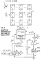
- Fig.1 The environment or general system in which the present invention is used is shown in Fig.1. It may be a communication system, or a magnetic or optical recording system of the partial-response class-IV type.
- Fig.1 represents a time-discrete model of such a system.
- a non-ideal PRIV channel is considered.
- the sequence ⁇ b n ⁇ (shown at 15) consists of correlated symbols from the (2M -1)-ary alphabet ⁇ 0, ⁇ 2, ... , ⁇ (2M - 2) ⁇ .
- the received signal appearing at the receiver input 19 is given by where ⁇ h n ⁇ is the inverse Fourier transform of H(f), and ⁇ n ⁇ is a sequence of i.i.d. Gaussian noise samples with zero mean and variance ⁇ 2.
- the signal sample x n is quantized in quantizer 21 and represented in binary notation by the (B + 1)-bit vector
- the quantized sample appearing at 23 is then given by where
- the quantizer output belongs to the interval ( -2M + 2 -B M , 2M - 2 -B M). It is assumed that the probability of the event ⁇
- the quantized samples appearing at 23 are processed in an adaptive equalizer 25 which is implemented as distributed-arithmetic equalizer.
- an adaptive equalizer 25 which is implemented as distributed-arithmetic equalizer.
- the look-up values of a fixed distributed-arithmetic equalizer are determined by the 2 N possible values of the vector precomputed and stored in a look-up table.
- k0 can be any index between 0 and N - 1.
- the number of look-up values to be stored is and determines whether the selected coefficient is to be added or subtracted.
- the look-up values are initially set such that the equalizer is equivalent to a linear filter with and are thereafter iteratively updated.
- the output values y n of equalizer 25 are furnished to a multilevel decision element 29 which provides at its output 31 a sequence of estimated symbols b ⁇ n .
- Block 35 represents the equalizer delay line for storing N consecutive (B + 1)-bit input values Bit positions are indicated by superscripts (0)...(w)...(B), and the consecutive modulation intervals are indicated by subscripts n...(n-k)...(n-N + 1). Each box 37 in block 35 represents a bit storage position. Each column contains a complete value each row contains the corresponding bits of all values stored in the delay line. When a new value is entered at input 23, all stored values are shifted by one position.
- the look-up values like the input values are also quantized and each represented by B d bits.
- Each (N-1)-bit address appearing on lines 39 causes fetching of one look-up value which is furnished on lines 43.
- This value is multiplied, in multiplying means 45, by a single bit which is available on line 47.
- This bit is one predetermined bit of the bit group presently used to compute an address for the look-up table, i.e., the corresponding bit of the input sample presently available at the predetermined tap of the delay line.
- the output of multiplying means 45 available on lines 49, is furnished to an accumulator arrangement comprising adder means 51, a register 53, and dividing means 55 which divides each register output by 2 (and which is actually a shifting means).
- the output of dividing means 55 is entered through lines 57 into adder means 51 where it is combined with the next partial value appearing on lines 49, the result being stored with the next clock pulse in register 53.
- a new equalizer output value y n is available on lines 27.
- This output value y n is then used to update, according to the invention, a single one of those look-up values stored in RAM 41 which were chosen in the current modulation interval for generating the output value y n . Details of the selection and updating procedure which is introduced by the invention are presented in the next sections C and D.
- Updating means 59 receives as inputs the equalizer output value y n on lines 27, and all addresses and corresponding look-up values chosen to compute y n , on lines 60 and 61, respectively.
- the single bits which previously appeared on line 47 are also provided on input 62.
- As output of the updating means 59 there appear on lines 63 and 64, respectively, a single updated look-up value and its corresponding address where w0 can be either B or (B-1).
- w0 can be either B or (B-1).
- the sequence ⁇ y n ⁇ is input to a multilevel memoryless decision element that generates the sequence of estimated symbols ⁇ b ⁇ n ⁇ .
- the mean-square error ⁇ 2 n defined by is considered, where ⁇ e n ⁇ is the error sequence and E denotes the expectation operator of the sequence ensemble. If the sequence ⁇ b n ⁇ were known at the receiver, i.e., if a training sequence were used, a reference-directed stochastic gradient algorithm could be used to update the look-up values of an adaptive distributed-arithmetic equalizer and to reach the setting yielding the minimum mean-square error. It is desirable that the system does not use a training sequence.
- the decision-directed adaptive distributed-arithmetic equalizer does not operate correctly if all the look-up values are simultaneously equal to 0. In fact, if that event occurs, then the equalizer output is equal to zero, as shown by Eq. (7). Hence, the estimated error is also equal to zero and adaptation terminates. Therefore it is assumed that
- the complexity of the system is reduced by the invention in that only one look-up value is updated at each iteration.
- the updating rate of the look-up values depends upon the joint probability distribution of the input samples, since the samples of the sequence ⁇ x q n ⁇ are correlated.
- a procedure randomly updating at each iteration either or is introduced by the invention.
- the simplified decision-directed stochastic gradient procedure is given by where ⁇ z n ⁇ is a sequence of binary i.i.d. random variables, z n ⁇ ⁇ 0, + 1 ⁇ , independent of the sequence ⁇ x n ⁇ , and ⁇ is chosen to be equal to a power of two, so that at each iteration only one shift-and-add operation is required.
- the stochastic gradient algorithm (12) fails, i.e., the look-up values do not converge to the optimum setting unless a training sequence is used.
- the self-training adaptation algorithms devised for linear adaptive equalizers fail if applied to a distributed-arithmetic equalizer. In fact, in that case the look-up values converge with high probability to non-optimal settings which correspond to local minima of the mean-square error.
- the updating rule (12) is applied whenever the distance between the output y n and any of the 2M - 1 output levels of an ideal system are smaller than a given positive constant ⁇ ⁇ 1.
- the look-up value is increased by a positive constant whenever condition (13) is not satisfied and the distance between y n and any of the output levels of an ideal system is larger than ⁇ .
- the look-up table updating procedure for self-training adaptive equalization is formulated as follows: where and where ⁇ 1 , ⁇ 2, and ⁇ 3 are positive constants.
- To compute the correction term defined in Eq.(17) is also represented by B d bits.
- FIG.3 An implementation of the adaptive distributed-arithmetic equalizer for a quaternary PRIV system, which operates according to the described principles of the invented updating procedure, is shown in Fig.3 (Fig.3A/3B).
- Units of this equalizer are controlled by several timing signals which are furnished by a timing signal generator 65 represented in Fig.4A and whose time diagrams are shown in Fig.4B.
- a timing signal generator 65 represented in Fig.4A and whose time diagrams are shown in Fig.4B.
- CL clock signal line 66
- P1...P4 phase signal pulses
- Binary selector signals S1...S4 furnished on lines 67 A...D, respectively, represent the four phase pulses. They are provided for selectively controlling the loading of registers, and for controlling several selectors each having four inputs and one output so that each one of the inputs appears at the selector output during one quarter of each modulation interval T.
- the equalizer of Fig.3 comprises a delay line 69 (corresponding to the delay line arrangement 35 in Fig.2) consisting of five six-bit registers RX0...RX4, storing quantized received input samples X q n furnished to input 23. Storing of each input sample in register RX0, and further shifting through the other registers is effected once during each sampling period by the phase pulse P3 of selector signal S3 on line 67C.
- the bits in the delay line registers are numbered b0 (least significant bit) through b5 (most significant bit).
- Output lines are so arranged that the first bits b0 of all five registers appear on lines 71A, the third bits b2 of all five registers appear on lines 71B, and the fifth bits b4 of all five registers appear on lines 71C. Similary, the five bits b1, b3, and b5 of all registers appear on lines 71D, 71E, and 71F, respectively.
- Table 1 The described arrangement is depicted in Table 1.
- Lines 71A, 71B, and 71C are conneted to three inputs of a selector 73 who also receives the three selector signals S1, S2, and S4 on lines 67A/B/D so that during three of the four quarter-intervals of each modulation interval, one of the five-bit input groups is selected.
- the four corresponding bits of registers RX0, RX1, RX3, and RX4 are then available on lines 77, and the respective corresponding bit bc-A of the register RX2 is available on line 79.
- each of the four bits on lines 77 is logically combined with the bit bc-A on line 79, and the resulting four-bit group is stored in register RA (83), once per clock interval, and is then available on lines 87 as an address for a dual-port random access memory (RAM 89) containing the look-up table of equalizer look-up values.
- register RA 83
- RAM 89 dual-port random access memory
- the bits appearing on delay line outputs 71 D, 71E, and 71F are similarly selected by a selector 91.
- the bits available on output lines 93, 95 are logically combined in XOR circuitry 97 and stored in register RB (99) once in each clock period, to become available as addresses on lines 101.
- An important feature of the present invention is the selection and updating of a single one of the fetched values from the look-up table.
- the first bit b0 in register RX0 is separately available as control bit z(0) on a line 111
- the first bit b0 stored in register RX1 is separately available as control bit z(1) on a line 113. They are also shown in Table 1.
- Each address pair A/B is presented to a selector 115, which depending on the binary value of the control bit z(0) on line 111, selects one address of the pair.
- One of the six addresses generated during each sampling interval (that corresponds to the address generated either by the most significant bits or by the second-most significant bits of the samples stored in the delay line) is stored, under control of phase pulse P4, in a delay register R12 (117), then shifted to a delay register R13 (119) in the next modulation interval, and then is transferred on lines 121 to the fourth input of selector 91 which also receives on a line 122 a fifth bit, set to a logical value of 1. Therefore, the address gated by selector 91 in quarter-interval P3 represented by selector signal S3, will become available during a quarter-interval P4 (when no values are read from the look-up table), as address iz on lines 101 for writing an updated value into the look-up table.
- the 12 bits of a look-up table output value VL-A, stored in register R1 and appearing on output lines 123, are each logically combined in XOR circuitry 129 with the corresponding bit bc-A from line 79 (which was delayed by a pair of delay elements 120 under control of the clock signal CL), then appearing on line 127. After division by a factor of 2 in element 130 and sign extension, the result becomes available as 14-bit input on lines 131 to an adder 133.
- each bit of an output value VL-B stored in register R2 and available on lines 137 is logically combined in XOR circuitry 143 with the corresponding bit bc-B from line 95 (delayed by delay element pair 139), then available on line 141. The result is sign-extended and becomes available on lines 145 as second input to adder 133.
- each adder output value (147) is stored in register R3 (149) and are then available on lines 151. They are stored with the next pulse of clock signal CL in a register R4 (153) and are then available also on lines 155.
- a selected one of the six values VL-A/VL-B and its companion single bit bcs are available on lines 159 and are stored in each modulation interval in a register R9 (161) under control of phase pulse P1 of selector signal S1 furnished on line 67A; the selected value d n , available on lines 163, is transferred in the next modulation interval to a register R10 (165).
- This value (corresponding to the value selected either by the most significant bits or by the second-most significant bits of the samples stored in the delay line) is then available on lines 163, its companion single bit bcs on a line 169.
- a selector 171 receives on its input lines 151 and 155 the contents of register R3 and register R4 and on its further input lines 173 a correction term (to be explained later), and selects each one of them in sequence per modulation interval under control of the selector signals S1...S4, for storing it through lines 175 in a register R5 (177).
- a selector 179 receives on its input lines 181 the contents of register R4 divided by 4 in a shifting circuit 183, on its input lines 167 the contents of register R10, and on its input lines 185 an input value which is generated from an output value (to be explained later) on lines 187, divided by 4 in a shifting circuit 189; it selects each one of them in sequence during a modulation interval, and stores them through lines 191 in a register R6 (193).
- the values stored in registers R5 and R6 are furnished through lines 195 and 197, respectively, to an adder 199. Its output which becomes available on lines 201 is stored with the next clock pulse in a register R7 (203).
- the eight most significant bits (205A) of the 12-bit output value on lines 205 are stored as equalizer output y n once per sampling interval (by phase pulse P1 of selector signal S1) in a register RY (207), and this value is furnished on lines 27 as equalizer output.
- the 12-bit output value on line 205 is also fed back via lines 187 (and divider 189) to input 185 of selector 179 (as an intermediate step for accumulating the next output value of the equalizer).
- the further circuitry of the equalizer shown in Fig.3 is used for updating a single look-up table value per sampling interval.
- the eight most significant bits (205A) are transferred to a correction term generator 209, which will be shown in more detail in Fig.5.
- the correction term generator also receives the selected single bit bcs available on line 169 (from register R9), and the control bit z(1) available on line 113.
- the generated correction term - ⁇ d n appearing on output lines 211 is stored, once per modulation interval, in a register R11 (213) under control of phase pulse P1 of selector signal S1. It is then available on lines 173 as input to selector 171.
- the value d n stored in register R10 (which is a selected one of six values chosen during one modulation interval), and the correction term furnished by generator 209, are gated by selectors 171/179 and transferred through registers R5 and R6 to be added in adder 199, and the result is then available as update term on lines 205.
- a limiter circuit 215 is provided which limits the update term from lines 205 between two preselected limit values, and the resulting updated look-up table value d n+1 is stored in a register R8 (217), under control of phase pulse P4 of selector signal S4.
- the contents of register R8 is transferred through lines 219 as input to RAM 89, and is stored therein under control of the then available address on lines 101, to replace the previously chosen look-up table value d n .
- the equalizer uses the bits of the stored received samples for generating addresses to choose look-up table values and combines these table values to generate one equalizer output y n per modulation interval.
- the equalizer circuitry selects one value d n of the look-up table values chosen for creating one output value y n , generates a correction term - ⁇ d n for it in dependence of the output, adds the correction term to d n , limits the result between two predetermined limit values, and stores it back as updated table value d n+1 to replace the selected table value d n .
- Fig.5 receives the current equalizer output value y n on lines 205A from register R7 (eight most significant bits). It receives further the control signal z(1) on line 113, and the selected single bit bcs on line 169, which represents the value appearing in equation (17) above.
- the correction term - ⁇ d n furnished at the output 211 of the correction term generator is chosen by a selector 225 among its three input values appearing on inputs 227, 229, and 231, under control of two binary control signals a 1,n and a 2,n furnished to two control inputs 233 and 235, respectively.
- Control signal a 1,n is generated as follows: From the input value y n on lines 205A, an estimated symbol is obtained by a 7-level decision circuit 237 whose characteristic is shown in Fig.7. The estimated symbol b ⁇ n appearing on lines 239 is subtracted from the input value y n in a subtractor 241 which, on its output 243, furnishes an estimated error value ê n . This estimated error value is furnished to a 2-level decision circuit 245 where the error value is compared to a first threshold t1 to obtain the binary control signal a 1,n on line 233. The characteristic of decision element 245 is shown in Fig.8.
- Control signal a 2,n is generated as follows: In a further 2-level decision circuit 247, the input value y n is compared against a second threshold t2 to obtain the binary control signal a 2,n on line 235. The characteristic of decision element 247 is shown in Fig.9.
- the three input values for selector 225 are generated as follows: In a power-of-two unit 249 (which actually is a shifting element), the control value z(1) appearing on line 113 is used to generate the three terms on lines 251, 253, and 255, respectively. Three constants ⁇ 1, ⁇ 2, ⁇ 3 are provided by registers 257, 259, and 261, respectively. The term appearing on line 251 is multiplied in multiplying unit 263 by constant ⁇ 1, to obtain on line 227 the value d 1,n which is furnished to the first input of selector 225.
- the term appearing on line 253 is multiplied in multiplying unit 265 by constant ⁇ 2, and the result is again multiplied in multiplying unit 267 by the error value ê n appearing on line 243, to generate an intermediate term on lines 269.
- This intermediate term is multiplied, in a multiplying unit 271, by the selected single bit bcs appearing on line 169, to obtain on lines 229 the value d 2,n as second input to selector 225. Since bcs is a single bit corresponding to the binary function the multiplier 271 is an XOR circuitry.
- the equalizer can be realized without any multiplier.
- Table 2 (separated into tables 2A and 2B) illustrates the sequential operational steps of the equalizer described above, by listing the contents of the various registers (RX1...RX5, R1...R13, RY) in sequential quarter-intervals of three consecutive modulation intervals T n ... T n+2. Each column of the table represents one quarter-interval, as indicated by a "1" in the respective P1/P2/P3/P4 row showing the phase pulses.
- the equalizer delay line consisting of the five registers RX1...RX5 initially holds five consecutive input samples In the middle of the first interval T n , a new input value enters the delay line at RX1, and the other values are shifted with the oldest value being dropped. Similarly, an enter-and-shift operation occurs in the middle of each following modulation interval.
- the bits of all samples stored in the delay line at the beginning of an interval are used, in six groups of corresponding bits, to generate six addresses i1 ... i6, which are available in three consecutive quarter-intervals in the two registers RA and RB, as shown in Tab.2A.
- Each pair of addresses are used to fetch two respective look-up table values which are then available (with one quarter-interval delay) in registers R1 and R2, respectively.
- Each pair of values (shown as VL-A and VL-B, respectively, in Fig.3) is combined by dividing the first value, e.g. d(i1), by two in a shifting element, and adding the result to the second value, e.g.
- register R7 By selective transfer operations between registers R3, R4 and R5, R6, R7, some of them with an intermediate division by a factor of 4, there will be available at the end of the second modulation interval T n+1 in register R7 (Tab.2B) a quantity which represents the output value y n (but with a twelve-bit precision instead of the final eight-bit precision at the equalizer output).
- This value in register R7 is a "weighted" sum of the three intermediate values J1, J2, J3, namely J3 + J2/4 + J1/16 (or d(i6) + d(i5)/2 + d(i4)/4 + d(i3)/8 + d(i2)/16 + + d(i1)/32). From the beginning of the next modulation interval T n+2 , the value y n (eight bits) is available in the output register RY.
- a selected one of the six look-up values d(i1)...d(i6) will be available as value d n in registers R9 and R10 during the second (T n+1 ) and third (T n+2 ) modulation intervals, respectively.
- the associated address iz will be available in registers R12 and R13 with a quarter-interval advance.
- the selected look-up value d n will be available in register R6, and an associated correction term - ⁇ d n (designated as -grad(n + 0) in the table) will be available in register R5, cf. Tab.2A.
- next quarter-interval P3
- Jd Jd in register R7
- This quantity is passed through a limiter, and is then availabe in the next quarter-interval (P4) as updated look-up value d n+1 (termed ud(n + 0) in the table) in register R8.
- This value is then stored in the look-up table, using the selected address iz (which was stored in register R13 and is transferred into register RB where it becomes available in the last quarter-interval (P4) of the third modulation interval).
- an output value y n becomes available in register RY at the end of the next interval T n+1 . Then, at the end of the following interval T n+2 one corresponding updated look-up value d n+1 becomes available in register R8, while the associated RAM address iz is then available in register RB.
Abstract
Description
- Present invention is concerned with adaptive equalization of channels for data transmission or storage, and in particular with a method of adapting a distributed-arithmetic equalizer by updating a look-up table containing values that determine the equalizer characteristics, and further with look-up table updating means in an adaptive distributed-arithmetic equalizer apparatus for channel equalization in a partial-response communication or storage system.
- A self-training adaptive equalization scheme is known from the the following publication: Y.Sato, "A Method of Self-Recovering Equalization for Multi-Level Amplitude Modulation Systems", IEEE Trans. Comm., Vol.COM-23, pp.679-682, June 1975. In the scheme disclosed, updating of the equalizer coefficients needs N multiplications as well as the computation of a particular function gk ; the latter requires, in the case of Partial-Response Class-IV (PRIV) signaling, an inversion of the PRIV channel and generation of a two-level PRIV signal. Furthermore, in the steady state the described linear adaptive equalizer undergoes enhanced tap noise with respect to a decision-directed adaptive equalizer.
- A new filter design was disclosed in an article by A.Peled et al. "A New Hardware Realization of Digital Filters", IEEE Trans. Acoustics, Speech, Signal Processing, Vol.ASSP-22, pp.456-462, December 1974. The new technique has become known as "distributed-arithmetic" filter design. However, the publication does not disclose any application of the filter as an adaptive equalizer.
- An adaptive equalizer using a distributed-arithmetic architecture was described in the following publication: C.F.N.Cowan et al., "A Digital Adaptive Filter Using a Memory-Accumulator Architecture: Theory and Realization", IEEE Trans. Acoustics, Speech, Signal Processing, Vol.ASSP-31, pp.541-549, June 1983. The look-up table value updating scheme disclosed in this article is based on a least mean-square algorithm, and no attempt is made to use the distributed-arithmetic equalizer in a self-training mode. For training the equalizer, transmission and recognition of a training sequence would normally be required.
- It would be desirable to have an equalization method and apparatus avoiding the disadvantages of known equalization devices and procedures.
- It is an object of the invention to provide an equalization scheme using a distributed-arithmetic technique, which is self-training on the received data signal and therefore needs no training sequence.
- It is another object to devise a self-training adaptive equalization scheme with low tap noise in the steady state.
- It is a further object to provide a self-training adaptive equalization scheme which allows a reduction in hardware complexity for the equalizer apparatus.
- These objects are achieved by an equalizing method as defined in
Claim 1, and by an equalizer apparatus as defined inClaim 7. -
- Fig.1 is a block diagram of the model of a system in which present invention is used;
- Fig.2 depicts the principle of an adaptive distributed-arithmetic equalizer according to the invention;
- Fig.3 (Fig.3A/3B) is a more detailed block diagram of the distributed-arithmetic equalizer of Fig.2;
- Fig.4A/Fig.4B are a block representation and a timing diagram for the clock and phase signals used in the equalizer of Fig.3;
- Fig.5 shows details of the correction term generator of the equalizer of Fig.3;
- Fig.6 is a diagram showing the correction term value vs. the equalizer output value for the case where

- Fig.7 shows the characteristic of the 7-level decision element in the correction term generator of Fig.5;
- Fig.8 shows the characteristic of the 2-level decision element with threshold t1 in the correction term generator of Fig.5;
- Fig.9 shows the characteristic of the 2-level decision element with threshold t2 in the correction term generator of Fig.5;
- The environment or general system in which the present invention is used is shown in Fig.1. It may be a communication system, or a magnetic or optical recording system of the partial-response class-IV type. Fig.1 represents a time-discrete model of such a system. The sequence of transmitted data {an} provided at
input 11 consists of independent and identically distributed (i.i.d.) symbols from the M-ary alphabet { ± 1, ± 3, ... , ± (M -1)}, M= 2m. A non-ideal PRIV channel is considered. The overall channel transfer function is modeled as the cascade of an ideal PRIV transfer function HPRIV(f) = 1 - e-j4πfT, (shown as block 13) where T is the modulation interval, and a transfer function H(f), (shown as block 17) which determines the channel distortion. Since a time-discrete model is considered, H(f) is a periodic function, the period of which is equal to the modulation rate
where Z is the set of integers. The output of an ideal PRIV channel is

which shows the introduction of controlled intersymbol interference (ISI). The sequence {bn} (shown at 15) consists of correlated symbols from the (2M -1)-ary alphabet {0, ± 2, ... , ± (2M - 2)} . The received signal appearing at thereceiver input 19 is given by
where {hn} is the inverse Fourier transform of H(f), and {νn} is a sequence of i.i.d. Gaussian noise samples with zero mean and variance ρ². - In the receiver, prior to equalization, the signal sample xn is quantized in quantizer 21 and represented in binary notation by the (B + 1)-bit vector

The quantized sample appearing at 23 is then given by
where
In the following, since there is one-to-one correpondence between
and
they will both be referred to as bits, bearing in mind that the former belong to the set { -1, +1}, the latter belong to the set {0, +1}. Note that the quantizer output belongs to the interval ( -2M + 2-BM , 2M - 2-BM). It is assumed that the probability of the event { |xn| > 2M} is negligible. Therefore the quantizer 21 is approximately equivalent to a uniform quantizer. - The quantized samples appearing at 23 are processed in an adaptive equalizer 25 which is implemented as distributed-arithmetic equalizer. Consider the vector c = {c₀, ... , cN-1} of coefficients of an N-tap linear equalizer, and the vector

of signals stored at time n in its delay line. The output of an equalizer with distributed-arithmetic architecture is computed as follows:
This shows that yn can be obtained as a weighted sum of B + 1 look-up values
for w = 0, ... , B. The look-up values of a fixed distributed-arithmetic equalizer are determined by the 2N possible values of the vector
precomputed and stored in a look-up table. - Since

and
differ only in their sign, i.e.,
only 2N-1 memory locations are needed. By exploiting this symmetry, (4) can be written in the form
where k₀ can be any index between 0 and N - 1. The number of look-up values to be stored is
and
determines whether the selected coefficient is to be added or subtracted. - The look-up values are initially set such that the equalizer is equivalent to a linear filter with

and are thereafter iteratively updated. The output of adaptive distributed-arithmetic equalizer 25, appearing at 27, is
where dn(j), j = 0, ... , 2N-1--1 , is the set of look-up values at the n-th iteration, and where the index
is given by
- The output values yn of equalizer 25 are furnished to a
multilevel decision element 29 which provides at its output 31 a sequence of estimated symbols b̂n. - The principles of an adaptive distributed-arithmetic equalizer using the invention are illustrated in Fig.2. It is assumed that the input values x

-
Block 35 represents the equalizer delay line for storing N consecutive (B + 1)-bit input values
Bit positions are indicated by superscripts (0)...(w)...(B), and the consecutive modulation intervals are indicated by subscripts n...(n-k)...(n-N + 1). Eachbox 37 inblock 35 represents a bit storage position. Each column contains a complete value
each row contains the corresponding bits
of all values stored in the delay line. When a new value is entered atinput 23, all stored values are shifted by one position. - During each modulation interval, all stored bits are read out sequentially. Each group of N corresponding bits with superscript (w) is used to compute an address (that appears on output lines 39) for the look-up table stored in random-
access memory 41, as shown by Eq.(8). - This look-up table contains 2N-1 look-up values dn(j) for j = 0, ... , 2N-1 - 1 , which determine the characteristics of the equalizer. They are selected using the bits of the stored values x

- The look-up values, like the input values

are also quantized and each represented by Bd bits. Each (N-1)-bit address
appearing onlines 39 causes fetching of one look-up value
which is furnished onlines 43. This value is multiplied, in multiplying means 45, by a single bit
which is available online 47. This bit is one predetermined bit of the bit group
presently used to compute an address for the look-up table, i.e., the corresponding bit
of the input sample presently available at the predetermined tap of the delay line. - The output of multiplying means 45, available on
lines 49, is furnished to an accumulator arrangement comprising adder means 51, aregister 53, and dividing means 55 which divides each register output by 2 (and which is actually a shifting means). The output of dividing means 55 is entered through lines 57 into adder means 51 where it is combined with the next partial value appearing onlines 49, the result being stored with the next clock pulse inregister 53. - Finally, at the end of each modulation interval, a new equalizer output value yn is available on
lines 27. This output value yn is then used to update, according to the invention, a single one of those look-up values stored inRAM 41 which were chosen in the current modulation interval for generating the output value yn. Details of the selection and updating procedure which is introduced by the invention are presented in the next sections C and D. - In Fig.2, only a schematic representation of this updating procedure is given. Updating means 59 receives as inputs the equalizer output value yn on
lines 27, and all addresses
and corresponding look-up values
chosen to compute yn, on lines 60 and 61, respectively. The single bits
which previously appeared online 47 are also provided oninput 62. As output of the updating means 59, there appear onlines 
and its corresponding address
where w₀ can be either B or (B-1). Hence, for updating there will be selected only one look-up value, either that adressed by the most significant bits (B) or that addressed by the second-most significant bits (B-1) presently stored in thedelay line 35. The selection between these two is determined by the procedure of the invention. - To determine equalizer performance, the sequence {yn} is input to a multilevel memoryless decision element that generates the sequence of estimated symbols {b̂n}. As a measure of system performance, the mean-square error ε


is considered, where {en} is the error sequence and E denotes the expectation operator of the sequence ensemble. If the sequence {bn} were known at the receiver, i.e., if a training sequence were used, a reference-directed stochastic gradient algorithm could be used to update the look-up values of an adaptive distributed-arithmetic equalizer and to reach the setting yielding the minimum mean-square error. It is desirable that the system does not use a training sequence. Therefore initial convergence of the look-up values is to be accomplished by self-training on the received data signal. A decision-directed stochastic gradient algorithm for the distributed-arithmetic adaptive equalizer presented above is formulated as follows:
where α is a positive constant,
and where ên = yn - b̂n is the estimated error, and δi,j is the Kronecker delta. - The decision-directed adaptive distributed-arithmetic equalizer does not operate correctly if all the look-up values are simultaneously equal to 0. In fact, if that event occurs, then the equalizer output is equal to zero, as shown by Eq. (7). Hence, the estimated error is also equal to zero and adaptation terminates. Therefore it is assumed that

- The complexity of the system is reduced by the invention in that only one look-up value is updated at each iteration. The updating rate of the look-up values depends upon the joint probability distribution of the input samples, since the samples of the sequence {x


or
is introduced by the invention. The simplified decision-directed stochastic gradient procedure is given by
where {zn} is a sequence of binary i.i.d. random variables, zn ∈ {0, + 1}, independent of the sequence {xn}, and α is chosen to be equal to a power of two, so that at each iteration only one shift-and-add operation is required. - In the presence of channel distortion, when adaptation starts the symbol error rate can be so large that the stochastic gradient algorithm (12) fails, i.e., the look-up values do not converge to the optimum setting unless a training sequence is used. On the other hand, because of the inherent nonlinearity of the system during the adaptation process, the self-training adaptation algorithms devised for linear adaptive equalizers fail if applied to a distributed-arithmetic equalizer. In fact, in that case the look-up values converge with high probability to non-optimal settings which correspond to local minima of the mean-square error.
- For linear adaptive equalizers, failure of decision-directed stochastic gradient algorithms is to be attributed to the large probability that the sign of the estimated error ên differs from the sign of the true error en . However, if the magnitude of the equalizer output yn is greater than the largest output level of an ideal system, i.e., if

then

where P{ω} denotes the probability of the event {ω}.
On the other hand, when the distributed-arithmetic realization considered inSection 2 is used and condition (13) is satisfied, Eq.(7) yields
In fact, since
if condition (13) is satisfied, then
with high probability. Consequently, the sign of the estimated error, which is related to the sign of the true error by Eq. (14), is also equal with high probability to both most significant bits of the sample
Therefore one finds that, whenever condition (13) is satisfied, the component of a gradient vector to update
is positive with probability close to one. - Moreover, it is required that the steady-state system performance be close to that of a system employing a reference-directed stochastic gradient algorithm. Therefore the updating rule (12) is applied whenever the distance between the output yn and any of the 2M - 1 output levels of an ideal system are smaller than a given positive constant γ < 1. Finally, to reduce the probability of convergence to settings yielding a large mean square error, the look-up value

is increased by a positive constant whenever condition (13) is not satisfied and the distance between yn and any of the output levels of an ideal system is larger than γ. - According to the invention, the look-up table updating procedure for self-training adaptive equalization is formulated as follows:

where
and where α₁ , α₂, and α₃ are positive constants. Fig.6 depicts Δdn versus yn for
and M = 4. To compute
the correction term defined in Eq.(17) is also represented by Bd bits. - An implementation of the adaptive distributed-arithmetic equalizer for a quaternary PRIV system, which operates according to the described principles of the invented updating procedure, is shown in Fig.3 (Fig.3A/3B).
- Units of this equalizer are controlled by several timing signals which are furnished by a
timing signal generator 65 represented in Fig.4A and whose time diagrams are shown in Fig.4B. During each modulation interval, four pulses of a clock signal CL will occur (clock signal line 66). Furthermore, four consecutive phase signal pulses P1...P4, one during each quarter of a modulation interval (quarter-interval), are available. Binary selector signals S1...S4, furnished onlines 67 A...D, respectively, represent the four phase pulses. They are provided for selectively controlling the loading of registers, and for controlling several selectors each having four inputs and one output so that each one of the inputs appears at the selector output during one quarter of each modulation interval T. - The equalizer of Fig.3 comprises a delay line 69 (corresponding to the
delay line arrangement 35 in Fig.2) consisting of five six-bit registers RX0...RX4, storing quantized received input samples X
- The bits in the delay line registers are numbered b0 (least significant bit) through b5 (most significant bit). Output lines are so arranged that the first bits b0 of all five registers appear on lines 71A, the third bits b2 of all five registers appear on lines 71B, and the fifth bits b4 of all five registers appear on
lines 71C. Similary, the five bits b1, b3, and b5 of all registers appear onlines -
Lines 71A, 71B, and 71C are conneted to three inputs of aselector 73 who also receives the three selector signals S1, S2, and S4 onlines 67A/B/D so that during three of the four quarter-intervals of each modulation interval, one of the five-bit input groups is selected. The four corresponding bits of registers RX0, RX1, RX3, and RX4 are then available onlines 77, and the respective corresponding bit bc-A of the register RX2 is available on line 79. In XOR circuitry 81, each of the four bits onlines 77 is logically combined with the bit bc-A on line 79, and the resulting four-bit group is stored in register RA (83), once per clock interval, and is then available onlines 87 as an address for a dual-port random access memory (RAM 89) containing the look-up table of equalizer look-up values. - The bits appearing on delay line outputs 71 D, 71E, and 71F are similarly selected by a
selector 91. The bits available onoutput lines XOR circuitry 97 and stored in register RB (99) once in each clock period, to become available as addresses onlines 101. - Thus, during three of the quarter-intervals of each sampling interval, i.e., those defined by S4, S1, and S2, a pair of addresses A and B becomes available. The two addressed stored values are fetched from the look-up table, and are then furnished on
lines - An important feature of the present invention is the selection and updating of a single one of the fetched values from the look-up table. For this purpose, the first bit b0 in register RX0 is separately available as control bit z(0) on a
line 111, and the first bit b0 stored in register RX1 is separately available as control bit z(1) on aline 113. They are also shown in Table 1. - For later restoring of one updated look-up table value, one of the six addresses becoming available on
lines RAM 89, is selected and delayed. Each address pair A/B is presented to aselector 115, which depending on the binary value of the control bit z(0) online 111, selects one address of the pair. One of the six addresses generated during each sampling interval (that corresponds to the address generated either by the most significant bits or by the second-most significant bits of the samples stored in the delay line) is stored, under control of phase pulse P4, in a delay register R12 (117), then shifted to a delay register R13 (119) in the next modulation interval, and then is transferred onlines 121 to the fourth input ofselector 91 which also receives on a line 122 a fifth bit, set to a logical value of 1. Therefore, the address gated byselector 91 in quarter-interval P3 represented by selector signal S3, will become available during a quarter-interval P4 (when no values are read from the look-up table), as address iz onlines 101 for writing an updated value into the look-up table. - The 12 bits of a look-up table output value VL-A, stored in register R1 and appearing on
output lines 123, are each logically combined inXOR circuitry 129 with the corresponding bit bc-A from line 79 (which was delayed by a pair of delay elements 120 under control of the clock signal CL), then appearing online 127. After division by a factor of 2 inelement 130 and sign extension, the result becomes available as 14-bit input onlines 131 to anadder 133. Similarly, each bit of an output value VL-B stored in register R2 and available onlines 137, is logically combined inXOR circuitry 143 with the corresponding bit bc-B from line 95 (delayed by delay element pair 139), then available online 141. The result is sign-extended and becomes available onlines 145 as second input to adder 133. - The twelve most significant bits of each adder output value (147) are stored in register R3 (149) and are then available on
lines 151. They are stored with the next pulse of clock signal CL in a register R4 (153) and are then available also onlines 155. - The two look-up table output values VL-A and VL-B stored in registers R1 and R2 and available on
lines 123/137, and the corresponding single bits bc-A and bc-B (called "companion" single bits in the following), available onlines 127/141, are furnished to aselector 157, which selects, determined by the value of control bit z(0), one of these two values and its companion single bit. A selected one of the six values VL-A/VL-B and its companion single bit bcs (selected companion bit) are available onlines 159 and are stored in each modulation interval in a register R9 (161) under control of phase pulse P1 of selector signal S1 furnished online 67A; the selected value dn , available onlines 163, is transferred in the next modulation interval to a register R10 (165). This value (corresponding to the value selected either by the most significant bits or by the second-most significant bits of the samples stored in the delay line) is then available onlines 163, its companion single bit bcs on aline 169. - A
selector 171 receives on itsinput lines lines 175 in a register R5 (177). Similarly, aselector 179 receives on itsinput lines 181 the contents of register R4 divided by 4 in a shiftingcircuit 183, on itsinput lines 167 the contents of register R10, and on itsinput lines 185 an input value which is generated from an output value (to be explained later) onlines 187, divided by 4 in a shiftingcircuit 189; it selects each one of them in sequence during a modulation interval, and stores them throughlines 191 in a register R6 (193). - The values stored in registers R5 and R6 are furnished through
lines adder 199. Its output which becomes available onlines 201 is stored with the next clock pulse in a register R7 (203). The eight most significant bits (205A) of the 12-bit output value onlines 205 are stored as equalizer output yn once per sampling interval (by phase pulse P1 of selector signal S1) in a register RY (207), and this value is furnished onlines 27 as equalizer output. In one of the quarter-intervals the 12-bit output value online 205 is also fed back via lines 187 (and divider 189) to input 185 of selector 179 (as an intermediate step for accumulating the next output value of the equalizer). - The further circuitry of the equalizer shown in Fig.3 is used for updating a single look-up table value per sampling interval. Of the value stored in register R7, available on
lines 205, the eight most significant bits (205A) are transferred to acorrection term generator 209, which will be shown in more detail in Fig.5. At its inputs, the correction term generator also receives the selected single bit bcs available on line 169 (from register R9), and the control bit z(1) available online 113. The generated correction term - Δdn appearing onoutput lines 211 is stored, once per modulation interval, in a register R11 (213) under control of phase pulse P1 of selector signal S1. It is then available onlines 173 as input toselector 171. Once per modulation interval the value dn stored in register R10 (which is a selected one of six values chosen during one modulation interval), and the correction term furnished bygenerator 209, are gated byselectors 171/179 and transferred through registers R5 and R6 to be added inadder 199, and the result is then available as update term onlines 205. - A limiter circuit 215 is provided which limits the update term from
lines 205 between two preselected limit values, and the resulting updated look-up table value dn+1 is stored in a register R8 (217), under control of phase pulse P4 of selector signal S4. The contents of register R8 is transferred throughlines 219 as input toRAM 89, and is stored therein under control of the then available address onlines 101, to replace the previously chosen look-up table value dn. - To summarize: The equalizer uses the bits of the stored received samples for generating addresses to choose look-up table values and combines these table values to generate one equalizer output yn per modulation interval. In addition, the equalizer circuitry selects one value dn of the look-up table values chosen for creating one output value yn, generates a correction term - Δdn for it in dependence of the output, adds the correction term to dn, limits the result between two predetermined limit values, and stores it back as updated table value dn+1 to replace the selected table value dn.
- Some more details of the
correction term generator 209 of Fig.3 are shown in Fig.5. It receives the current equalizer output value yn onlines 205A from register R7 (eight most significant bits). It receives further the control signal z(1) online 113, and the selected single bit bcs online 169, which represents the value
appearing in equation (17) above. - The correction term - Δdn furnished at the
output 211 of the correction term generator, is chosen by aselector 225 among its three input values appearing oninputs control inputs - Fig.6 shows the correction term Δdn as a function of yn, for

and M=4. - Control signal a1,n is generated as follows: From the input value yn on
lines 205A, an estimated symbol is obtained by a 7-level decision circuit 237 whose characteristic is shown in Fig.7. The estimated symbol b̂n appearing onlines 239 is subtracted from the input value yn in asubtractor 241 which, on itsoutput 243, furnishes an estimated error value ên. This estimated error value is furnished to a 2-level decision circuit 245 where the error value is compared to a first threshold t₁ to obtain the binary control signal a1,n online 233. The characteristic ofdecision element 245 is shown in Fig.8. - Control signal a2,n is generated as follows: In a further 2-
level decision circuit 247, the input value yn is compared against a second threshold t₂ to obtain the binary control signal a2,n online 235. The characteristic ofdecision element 247 is shown in Fig.9. - The three input values for
selector 225 are generated as follows: In a power-of-two unit 249 (which actually is a shifting element), the control value z(1) appearing online 113 is used to generate the three terms
onlines registers line 251 is multiplied in multiplyingunit 263 by constant α₁, to obtain online 227 the value d1,n which is furnished to the first input ofselector 225. - The term appearing on
line 253 is multiplied in multiplyingunit 265 by constant α₂, and the result is again multiplied in multiplyingunit 267 by the error value ên appearing online 243, to generate an intermediate term onlines 269. This intermediate term is multiplied, in a multiplyingunit 271, by the selected single bit bcs appearing online 169, to obtain onlines 229 the value d2,n as second input toselector 225. Since bcs is a single bit corresponding to the binary function
themultiplier 271 is an XOR circuitry. - The term on
line 255 is multiplied, in a multiplyingunit 273, by the third constant α₃, to obtain onlines 231 the value d3,n as third input forselector 225. - If the three constants α₁, α₂, α₃ are chosen to be positive integers and powers of two, then the
registers units - Table 2 (separated into tables 2A and 2B) illustrates the sequential operational steps of the equalizer described above, by listing the contents of the various registers (RX1...RX5, R1...R13, RY) in sequential quarter-intervals of three consecutive modulation intervals Tn ... Tn+2. Each column of the table represents one quarter-interval, as indicated by a "1" in the respective P1/P2/P3/P4 row showing the phase pulses.
- The equalizer delay line consisting of the five registers RX1...RX5 initially holds five consecutive input samples

In the middle of the first interval Tn, a new input value
enters the delay line at RX1, and the other values are shifted with the oldest value being dropped. Similarly, an enter-and-shift operation occurs in the middle of each following modulation interval. - The bits of all samples stored in the delay line at the beginning of an interval are used, in six groups of corresponding bits, to generate six addresses i1 ... i6, which are available in three consecutive quarter-intervals in the two registers RA and RB, as shown in Tab.2A. Each pair of addresses are used to fetch two respective look-up table values which are then available (with one quarter-interval delay) in registers R1 and R2, respectively. Each pair of values (shown as VL-A and VL-B, respectively, in Fig.3) is combined by dividing the first value, e.g. d(i1), by two in a shifting element, and adding the result to the second value, e.g. d(i2), to obtain an intermediate value J1, which is stored in the next quarter-interval in register R3. Thus, as shown in Tab.2A, three intermediate values J1, J2, and J3 are avaiable in consecutive quarter-intervals in register R3. With another delay of one quarter-interval, the same values are then also available in register R4.
- By selective transfer operations between registers R3, R4 and R5, R6, R7, some of them with an intermediate division by a factor of 4, there will be available at the end of the second modulation interval Tn+1 in register R7 (Tab.2B) a quantity which represents the output value yn (but with a twelve-bit precision instead of the final eight-bit precision at the equalizer output). This value in register R7 is a "weighted" sum of the three intermediate values J1, J2, J3, namely J3 + J2/4 + J1/16 (or d(i6) + d(i5)/2 + d(i4)/4 + d(i3)/8 + d(i2)/16 + + d(i1)/32). From the beginning of the next modulation interval Tn+2, the value yn (eight bits) is available in the output register RY.
- A selected one of the six look-up values d(i1)...d(i6) will be available as value dn in registers R9 and R10 during the second (Tn+1) and third (Tn+2) modulation intervals, respectively. The associated address iz will be available in registers R12 and R13 with a quarter-interval advance. In the second quarter-interval (P2) of the third modulation interval Tn+2, the selected look-up value dn will be available in register R6, and an associated correction term - Δdn (designated as -grad(n + 0) in the table) will be available in register R5, cf. Tab.2A. Both are combined in an adding operation and the result is available in the next quarter-interval (P3) as intermdiate term Jd in register R7, cf. Tab.2B. This quantity is passed through a limiter, and is then availabe in the next quarter-interval (P4) as updated look-up value dn+1 (termed ud(n + 0) in the table) in register R8. This value is then stored in the look-up table, using the selected address iz (which was stored in register R13 and is transferred into register RB where it becomes available in the last quarter-interval (P4) of the third modulation interval).
- Thus, based on the samples stored in the equalizer delay line at the beginning of interval Tn, an output value yn becomes available in register RY at the end of the next interval Tn+1. Then, at the end of the following interval Tn+2 one corresponding updated look-up value dn+1 becomes available in register R8, while the associated RAM address iz is then available in register RB.


Claims (12)
- Method of adapting a distributed-arithmetic equalizer by updating table values dn(j) stored in a look-up table, which determine the equalizer characteristics,
each equalizer output value yn being obtained by fetching table values dn(j) from the look-up table, using the bits representing stored received signal samples x
characterized by the execution of following steps in each modulation interval:- obtaining a single predetermined bit z(0) of the whole set of stored signal samples x - updating only one table value dn by selecting, in dependence of the binary control value, one of those table values which were fetched for obtaining an equalizer output value yn , adding a correction term - Δdn which is generated in dependence of said equalizer output value yn and said binary control value zn to said one selected table value dn, limiting the result between two predetermined values, and storing it back as updated table value dn+1.
 - Method according to Claim 1, characterized in that said correction term - Δdn is obtained by the steps of:- comparing the equalizer output value yn to a target set of symbols which is determined by the modulation scheme being used;- choosing - Δdn equal to f₁(zn) if |yn| is greater than (M + γ), where f₁ is a predetermined first function of said binary control value, M is the largest value in the target set of symbols, and γ is a first predetermined constant;- choosing - Δdn equal


 - choosing - Δdn equal to f₃(zn) otherwise, where f₃ is a predetermined third function of said binary control value.
 - Method according to Claim 1 or 2, characterized by the steps of:- storing N signal samples x
 - forming (B + 1) addresses for fetching look-up table values, each from a group of N corresponding bits
 - preselecting a given pair (VL-A, VL-B) of all fetched look-up table values, and the associated pair of predetermined companion bits (bc-A, bc-B) used for generating their addresses; and- using the binary control value zn for finally selecting one look-up table value dn of said pair for updating, and for selecting its associated predetermined companion bit (bcs) as additional input for generating said correction term - Δdn.
 - Method according to Claim 2, characterized in that said predetermined first function is obtained as

- Method according to Claim 2, characterized in that said predetermined second function is obtained as

- Method according to Claim 2, characterized in that said predetermined third function is obtained as

- Equalizer apparatus for channel equalization in a partial-response communication or storage system, said apparatus comprising a delay line for storing sequentially received signal samples x

characterized by look-up table value updating means comprising:- means (111; 113) for obtaining a predetermined one (z(0); z(1)) of all bits stored in said delay line, as binary control value zn;- means (157, 161) for selecting one of the fetched table values dn(j) from the look-up table, under control of said binary control value zn furnished to it;- means (209) for providing a correction term - Δdn in response to the binary control value and the equalizer output value;- means (171, 177, 179, 193, 199, 203) for causing addition of the one selected table value dn and the generated correction term - Δdn to obtain an intermediate term;- means (215) for limiting the intermediate term between predetermined limit values, furnishing at its output an updated look-up table value dn+1; and- means (115, 117, 119, 217, 219) for causing storage of the updated table value dn+1 in said look-up table. - Equalizer apparatus according to Claim 7, characterized in that said means (209) for providing a correction term - Δdn include:- means (237) for comparing the equalizer output value yn to a target set of symbols which is determined by the modulation scheme being used;- first means (249, 257, 263) for generating the correction term - Δdn as a first predetermined function f₁(zn) of said binary control value if the equalizer output value is greater than the sum of the largest symbol M of the target set and a first constant γ;- second means (241, 249, 259, 265, 267, 271) for generating the correction term - Δdn as the product of a second predetermined function f₂(zn) of said binary control value, a binary function
 - third means (249, 261, 273) for generating the correction term - Δdn as a third function f₃(zn) of said binary control value in all other cases.
 - Equalizer apparatus according to Claim 7 or 8, characterized in that said selecting means (157, 161) includes:- a selector (157) having two input groups (123, 127; 137, 141), each for receiving one fetched table value (VL-A, VL-B) and a corresponding predetermined companion bit (bc-A, bc-B) that was used for generating its address, and having a control terminal (111) for receiving said binary control value zn, for obtaining one selected table value and its associated companion bit at the selector output (159); and- register means (161) for storing, under control of a given timing signal pulse (S1/P1), a single one of sequential output values from said selector, as said selected table value dn, and its associated companion bit bcs.
- Equalizer apparatus according to Claim 8, characterized in that said first generating means (249, 257, 263) includes:- means (249) for generating a first power term
 - means (257, 263) for multiplying said first power term by a predetermined first power of two (α₁).
 - Equalizer apparatus according to Claim 8, characterized in that said second generating means (241, 249, 259, 265, 267, 271) includes:- means (249) for generating a second power term
 - means (259, 265) for multiplying said second power term by a predetermined second power of two (α₂), to obtain a first intermediate term,- means (241) for generating an error value ên from said equalizer output value yn and an output value b̂n of said comparing means (237);- means (267) for multiplying said first intermediate term by said error value to obtain a second intermediate term; and- means (271) for multiplying said second intermediate term by a binary function
- Equalizer apparatus according to Claim 8, characterized in that said third generating means (249, 261, 273) includes:- means (249) for generating a third power term
 - means (261, 273) for multiplying said third power term by a predetermined third power of two (α₃).
Priority Applications (4)
| Application Number | Priority Date | Filing Date | Title |
|---|---|---|---|
| DE69020568T DE69020568D1 (en) | 1990-10-30 | 1990-10-30 | Self-training adaptive equalization method and device. |
| EP90810828A EP0483439B1 (en) | 1990-10-30 | 1990-10-30 | Self-training adaptive equalization method and apparatus |
| JP3194819A JPH0793594B2 (en) | 1990-10-30 | 1991-07-09 | Self-training adaptive equalizer |
| US07/781,538 US5319674A (en) | 1990-10-30 | 1991-10-22 | Method for self-training adaptive equalization |
Applications Claiming Priority (1)
| Application Number | Priority Date | Filing Date | Title |
|---|---|---|---|
| EP90810828A EP0483439B1 (en) | 1990-10-30 | 1990-10-30 | Self-training adaptive equalization method and apparatus |
Publications (2)
| Publication Number | Publication Date |
|---|---|
| EP0483439A1 true EP0483439A1 (en) | 1992-05-06 |
| EP0483439B1 EP0483439B1 (en) | 1995-06-28 |
Family
ID=8205964
Family Applications (1)
| Application Number | Title | Priority Date | Filing Date |
|---|---|---|---|
| EP90810828A Expired - Lifetime EP0483439B1 (en) | 1990-10-30 | 1990-10-30 | Self-training adaptive equalization method and apparatus |
Country Status (4)
| Country | Link |
|---|---|
| US (1) | US5319674A (en) |
| EP (1) | EP0483439B1 (en) |
| JP (1) | JPH0793594B2 (en) |
| DE (1) | DE69020568D1 (en) |
Cited By (3)
| Publication number | Priority date | Publication date | Assignee | Title |
|---|---|---|---|---|
| WO2001084724A2 (en) * | 2000-04-28 | 2001-11-08 | Broadcom Corporation | Methods and systems for adaptive receiver equalization |
| US7245638B2 (en) | 2000-07-21 | 2007-07-17 | Broadcom Corporation | Methods and systems for DSP-based receivers |
| US7564866B2 (en) | 2000-07-21 | 2009-07-21 | Broadcom Corporation | Methods and systems for digitally processing optical data signals |
Families Citing this family (27)
| Publication number | Priority date | Publication date | Assignee | Title |
|---|---|---|---|---|
| US5268848A (en) | 1992-09-30 | 1993-12-07 | International Business Machines Corporation | Equalizer adjustment for partial-response maximum-likelihood disk drive systems |
| CA2185126C (en) * | 1994-03-09 | 2005-09-27 | Michael Rodney Walker | Method and apparatus for decreasing modem retraining due to blank and burst signalling in analog cellular systems |
| DE69427135T2 (en) * | 1994-12-28 | 2001-09-13 | Ibm | ADAPTIVE EQUALIZATION FOR PRIVATE TRANSMISSION SYSTEMS |
| FR2740286B1 (en) * | 1995-10-23 | 1998-01-02 | Inst Eurecom | DEVICE AND METHOD FOR HYBRID DIGITAL-ANALOG COMMUNICATION ON A TELEPHONE CHANNEL |
| US6819514B1 (en) | 1996-04-30 | 2004-11-16 | Cirrus Logic, Inc. | Adaptive equalization and interpolated timing recovery in a sampled amplitude read channel for magnetic recording |
| US5999355A (en) | 1996-04-30 | 1999-12-07 | Cirrus Logic, Inc. | Gain and phase constrained adaptive equalizing filter in a sampled amplitude read channel for magnetic recording |
| US5892632A (en) * | 1996-11-18 | 1999-04-06 | Cirrus Logic, Inc. | Sampled amplitude read channel employing a residue number system FIR filter in an adaptive equalizer and in interpolated timing recovery |
| US5978379A (en) | 1997-01-23 | 1999-11-02 | Gadzoox Networks, Inc. | Fiber channel learning bridge, learning half bridge, and protocol |
| US6049574A (en) * | 1998-04-17 | 2000-04-11 | Trustees Of Tufts College | Blind adaptive equalization using cost function that measures dissimilarity between the probability distributions of source and equalized signals |
| US6704317B1 (en) | 1998-05-27 | 2004-03-09 | 3Com Corporation | Multi-carrier LAN modem server |
| US6507585B1 (en) | 1998-05-27 | 2003-01-14 | 3Com Corporation | Multi-carrier LAN adapter device using frequency domain equalizer |
| US6891887B1 (en) | 1998-05-27 | 2005-05-10 | 3Com Corporation | Multi-carrier LAN adapter device using interpolative equalizer |
| US6377683B1 (en) | 1998-05-29 | 2002-04-23 | 3Com Corporation | Low complexity frequency domain echo canceller for DMT transceivers |
| US6603811B1 (en) | 1998-05-29 | 2003-08-05 | 3Com Corporation | Low complexity frequency domain equalizer having fast re-lock |
| US6643271B1 (en) | 1999-04-30 | 2003-11-04 | 3Com Corporation | Adjustable gain transmit cancellation in a full-duplex modem data access arrangement (DAA) |
| US6751202B1 (en) | 1999-04-30 | 2004-06-15 | 3Com Corporation | Filtered transmit cancellation in a full-duplex modem data access arrangement (DAA) |
| GB2392066B (en) * | 2002-08-16 | 2005-11-09 | Toshiba Res Europ Ltd | Equaliser apparatus and methods |
| US20050201457A1 (en) * | 2004-03-10 | 2005-09-15 | Allred Daniel J. | Distributed arithmetic adaptive filter and method |
| US7774398B2 (en) * | 2005-05-10 | 2010-08-10 | Adaptive Spectrum And Signal Alignment, Inc. | Tonal rotors |
| US7991122B2 (en) | 2005-06-02 | 2011-08-02 | Adaptive Spectrum And Signal Alignment, Inc. | DSL system training |
| US20070147491A1 (en) * | 2005-12-22 | 2007-06-28 | Intel Corporation | Transmitter equalization |
| US20140369480A1 (en) | 2013-06-12 | 2014-12-18 | Adaptive Spectrum And Signal Alignment, Inc. | Systems, methods, and apparatuses for implementing a dsl system |
| EP2030454B2 (en) * | 2006-06-06 | 2016-09-07 | Adaptive Spectrum and Signal Alignment, Inc. | Vectored dsl system |
| CN101621305B (en) * | 2008-06-30 | 2012-08-29 | 富士通株式会社 | Base band predistortion device and method |
| JP5570250B2 (en) * | 2010-03-04 | 2014-08-13 | 地方独立行政法人 岩手県工業技術センター | Adaptive filter |
| US8737490B1 (en) * | 2010-08-20 | 2014-05-27 | Cadence Design Systems, Inc. | Analog-to-digital converter based decision feedback equalization |
| US8737491B1 (en) | 2010-08-20 | 2014-05-27 | Cadence Design Systems, Inc. | Analog-to-digital converter based decision feedback equalization |
Citations (1)
| Publication number | Priority date | Publication date | Assignee | Title |
|---|---|---|---|---|
| EP0057953A2 (en) * | 1981-02-11 | 1982-08-18 | Koninklijke Philips Electronics N.V. | Arrangement for correcting pulse distortion in homochronous data transmission |
Family Cites Families (9)
| Publication number | Priority date | Publication date | Assignee | Title |
|---|---|---|---|---|
| GB8400791D0 (en) * | 1984-01-12 | 1984-02-15 | British Telecomm | Digital filter |
| US4829463A (en) * | 1985-03-27 | 1989-05-09 | Akai Electric Co. Ltd. | Programmed time-changing coefficient digital filter |
| US4635276A (en) * | 1985-07-25 | 1987-01-06 | At&T Bell Laboratories | Asynchronous and non-data decision directed equalizer adjustment |
| JPH01149618A (en) * | 1987-12-07 | 1989-06-12 | Nec Corp | Decision feedback type equalization system |
| JPH0757012B2 (en) * | 1989-04-13 | 1995-06-14 | 日本ビクター株式会社 | Ghost removal device |
| JPH0421207A (en) * | 1990-05-16 | 1992-01-24 | Oki Electric Ind Co Ltd | Adaptive equalizer |
| JP2503726B2 (en) * | 1990-05-25 | 1996-06-05 | 日本電気株式会社 | Decision feedback equalizer |
| JPH0481015A (en) * | 1990-07-20 | 1992-03-13 | Fujitsu Ltd | Digital variable equalizer |
| US5132988A (en) * | 1990-12-03 | 1992-07-21 | Board Of Trustees, Leland Stanford Jr. University | Adaptive decision feedback equalizer apparatus for processing information stored on digital storage media |
-
1990
- 1990-10-30 DE DE69020568T patent/DE69020568D1/en not_active Expired - Lifetime
- 1990-10-30 EP EP90810828A patent/EP0483439B1/en not_active Expired - Lifetime
-
1991
- 1991-07-09 JP JP3194819A patent/JPH0793594B2/en not_active Expired - Lifetime
- 1991-10-22 US US07/781,538 patent/US5319674A/en not_active Expired - Fee Related
Patent Citations (1)
| Publication number | Priority date | Publication date | Assignee | Title |
|---|---|---|---|---|
| EP0057953A2 (en) * | 1981-02-11 | 1982-08-18 | Koninklijke Philips Electronics N.V. | Arrangement for correcting pulse distortion in homochronous data transmission |
Non-Patent Citations (1)
| Title |
|---|
| IEEE TRANSACTIONS ON ACOUSTICS, SPEECH, AND SIGNAL PROCESSING, vol. ASSP-31, no. 3, June 1983, pages 541-549, New York, US; C.F.N. COWAN et al.. "A digital adaptive filter using a memory-accumulator architecture: Theory and realization" * |
Cited By (15)
| Publication number | Priority date | Publication date | Assignee | Title |
|---|---|---|---|---|
| US7286597B2 (en) | 2000-04-28 | 2007-10-23 | Broadcom Corporation | Methods and systems for adaptive receiver equalization |
| US8223828B2 (en) | 2000-04-28 | 2012-07-17 | Broadcom Corporation | Methods and systems for adaptive receiver equalization |
| US6509773B2 (en) | 2000-04-28 | 2003-01-21 | Broadcom Corporation | Phase interpolator device and method |
| US6791388B2 (en) | 2000-04-28 | 2004-09-14 | Broadcom Corporation | Phase interpolator device and method |
| US6995594B2 (en) | 2000-04-28 | 2006-02-07 | Broadcom Corporation | Phase interpolator device and method |
| US8824538B2 (en) | 2000-04-28 | 2014-09-02 | Broadcom Corporation | Methods and systems for adaptive receiver equalization |
| WO2001084724A3 (en) * | 2000-04-28 | 2002-05-23 | Broadcom Corp | Methods and systems for adaptive receiver equalization |
| US8798219B2 (en) | 2000-04-28 | 2014-08-05 | Broadcom Corporation | High-speed serial data transceiver and related methods |
| WO2001084724A2 (en) * | 2000-04-28 | 2001-11-08 | Broadcom Corporation | Methods and systems for adaptive receiver equalization |
| US8472512B2 (en) | 2000-04-28 | 2013-06-25 | Broadcom Corporation | Methods and systems for adaptive receiver equalization |
| US7564866B2 (en) | 2000-07-21 | 2009-07-21 | Broadcom Corporation | Methods and systems for digitally processing optical data signals |
| US8363683B2 (en) | 2000-07-21 | 2013-01-29 | Broadcom Corporation | Methods and systems for DSP-based receivers |
| US7835387B2 (en) | 2000-07-21 | 2010-11-16 | Broadcom Corporation | Methods and systems for digitally processing data signals |
| US7778286B2 (en) | 2000-07-21 | 2010-08-17 | Broadcom Corporation | Methods and systems for DSP-based receivers |
| US7245638B2 (en) | 2000-07-21 | 2007-07-17 | Broadcom Corporation | Methods and systems for DSP-based receivers |
Also Published As
| Publication number | Publication date |
|---|---|
| US5319674A (en) | 1994-06-07 |
| JPH0793594B2 (en) | 1995-10-09 |
| EP0483439B1 (en) | 1995-06-28 |
| JPH04227129A (en) | 1992-08-17 |
| DE69020568D1 (en) | 1995-08-03 |
Similar Documents
| Publication | Publication Date | Title |
|---|---|---|
| EP0483439B1 (en) | Self-training adaptive equalization method and apparatus | |
| US4564952A (en) | Compensation of filter symbol interference by adaptive estimation of received symbol sequences | |
| JP2960436B2 (en) | Receiver for nonlinear data transmission system | |
| US4435823A (en) | Adaptive equalizer capable of linear and nonlinear weighting | |
| US5214671A (en) | Adaptive equalizer | |
| US4021738A (en) | Adaptive equalizer with fast convergence properties | |
| KR960012019B1 (en) | Hdtv channel equipment | |
| EP0363551B1 (en) | Adaptive equalization for recording systems using partial-response signaling | |
| US4237554A (en) | Coefficient tap leakage for fractionally-spaced equalizers | |
| US5617450A (en) | Digital subscriber loop interface unit | |
| US3633105A (en) | Digital adaptive equalizer system | |
| US5491518A (en) | Equalization apparatus with fast coefficient updating operation | |
| GB2247812A (en) | Equalizer for linear modulated signal on radio channel | |
| US4633482A (en) | Method of and arrangement for determining the optimum position of the reference tap of an adaptive equalizer | |
| GB1591545A (en) | Frequency domain equalizer | |
| US5291523A (en) | Viterbi receiver with improved timing means | |
| US5594756A (en) | Decision feedback equalization circuit | |
| US5586068A (en) | Adaptive electronic filter | |
| US5923226A (en) | Automatic equalizer | |
| US5995544A (en) | Adaptive equalization for PRIV transmission systems | |
| Lender | Decision-directed digital adaptive equalization technique for high-speed data transmission | |
| US20070014345A1 (en) | Low complexity Tomlinson-Harashima precoders | |
| Newhall et al. | A technique for finding approximate inverse systems and its applications to equalization | |
| US5898731A (en) | Auto-coefficient renewal digital channel equalizer | |
| US4233683A (en) | Cascaded equalizer technique |
Legal Events
| Date | Code | Title | Description |
|---|---|---|---|
| PUAI | Public reference made under article 153(3) epc to a published international application that has entered the european phase |
Free format text: ORIGINAL CODE: 0009012 |
|
| AK | Designated contracting states |
Kind code of ref document: A1 Designated state(s): DE FR GB |
|
| 17P | Request for examination filed |
Effective date: 19920917 |
|
| 17Q | First examination report despatched |
Effective date: 19940919 |
|
| GRAA | (expected) grant |
Free format text: ORIGINAL CODE: 0009210 |
|
| AK | Designated contracting states |
Kind code of ref document: B1 Designated state(s): DE FR GB |
|
| REF | Corresponds to: |
Ref document number: 69020568 Country of ref document: DE Date of ref document: 19950803 |
|
| ET | Fr: translation filed | ||
| PG25 | Lapsed in a contracting state [announced via postgrant information from national office to epo] |
Ref country code: DE Effective date: 19950929 |
|
| PLBE | No opposition filed within time limit |
Free format text: ORIGINAL CODE: 0009261 |
|
| STAA | Information on the status of an ep patent application or granted ep patent |
Free format text: STATUS: NO OPPOSITION FILED WITHIN TIME LIMIT |
|
| 26N | No opposition filed | ||
| PGFP | Annual fee paid to national office [announced via postgrant information from national office to epo] |
Ref country code: GB Payment date: 19960925 Year of fee payment: 7 |
|
| PGFP | Annual fee paid to national office [announced via postgrant information from national office to epo] |
Ref country code: FR Payment date: 19961007 Year of fee payment: 7 |
|
| PG25 | Lapsed in a contracting state [announced via postgrant information from national office to epo] |
Ref country code: GB Free format text: LAPSE BECAUSE OF NON-PAYMENT OF DUE FEES Effective date: 19971030 |
|
| PG25 | Lapsed in a contracting state [announced via postgrant information from national office to epo] |
Ref country code: FR Free format text: THE PATENT HAS BEEN ANNULLED BY A DECISION OF A NATIONAL AUTHORITY Effective date: 19971031 |
|
| GBPC | Gb: european patent ceased through non-payment of renewal fee |
Effective date: 19971030 |
|
| REG | Reference to a national code |
Ref country code: FR Ref legal event code: ST |