EP0484158A2 - Radio transceiver having PLL synthesizer - Google Patents
Radio transceiver having PLL synthesizer Download PDFInfo
- Publication number
- EP0484158A2 EP0484158A2 EP91310074A EP91310074A EP0484158A2 EP 0484158 A2 EP0484158 A2 EP 0484158A2 EP 91310074 A EP91310074 A EP 91310074A EP 91310074 A EP91310074 A EP 91310074A EP 0484158 A2 EP0484158 A2 EP 0484158A2
- Authority
- EP
- European Patent Office
- Prior art keywords
- signal
- frequency
- alarm
- radio frequency
- unlock
- Prior art date
- Legal status (The legal status is an assumption and is not a legal conclusion. Google has not performed a legal analysis and makes no representation as to the accuracy of the status listed.)
- Granted
Links
Images


Classifications
-
- H—ELECTRICITY
- H04—ELECTRIC COMMUNICATION TECHNIQUE
- H04B—TRANSMISSION
- H04B1/00—Details of transmission systems, not covered by a single one of groups H04B3/00 - H04B13/00; Details of transmission systems not characterised by the medium used for transmission
- H04B1/38—Transceivers, i.e. devices in which transmitter and receiver form a structural unit and in which at least one part is used for functions of transmitting and receiving
- H04B1/40—Circuits
- H04B1/44—Transmit/receive switching
-
- H—ELECTRICITY
- H03—ELECTRONIC CIRCUITRY
- H03L—AUTOMATIC CONTROL, STARTING, SYNCHRONISATION, OR STABILISATION OF GENERATORS OF ELECTRONIC OSCILLATIONS OR PULSES
- H03L7/00—Automatic control of frequency or phase; Synchronisation
- H03L7/06—Automatic control of frequency or phase; Synchronisation using a reference signal applied to a frequency- or phase-locked loop
- H03L7/08—Details of the phase-locked loop
- H03L7/085—Details of the phase-locked loop concerning mainly the frequency- or phase-detection arrangement including the filtering or amplification of its output signal
- H03L7/095—Details of the phase-locked loop concerning mainly the frequency- or phase-detection arrangement including the filtering or amplification of its output signal using a lock detector
Definitions
- the present invention relates to a radio transmitter/ receiver (referred to as "transceiver”, hereinafter) having an unlock alarm of a frequency synthesizer including a PLL (phase locked loop) as one of device alarms and, particularly, to such a transceiver suitable for use in a radio communication system such as a time division multiple access (TDMA) communications system which requires high-speed and frequent switching between a receiving state and a transmitting state.
- a radio transmitter/ receiver referred to as "transceiver”, hereinafter
- PLL phase locked loop
- the TDMA communications system is employed in many radio communications systems including a digital cellular telephone system according to Groupe Speciale Mobile (GSM) standard.
- GSM Groupe Speciale Mobile
- a single PLL frequency synthesizer is shared by a receiving portion and a transmitting portion of the transceiver as a local frequency source, since there is no simultaneous transmission and receiving.
- the shared use of the PLL frequency synthesizer is unavoidable.
- the PLL frequency synthesizer constituting the local frequency signal source should be durable against high-speed, highly frequent frequency switching.
- the PLL frequency synthesizer In order to operate the PLL frequency synthesizer normally, the PLL frequency synthesizer must be kept phase locked. Therefore, any out-of-phase condition, that is, unlock condition must be detected and corrected quickly. To this end, the PLL frequency synthesizer usually includes an unlock detection circuit for detecting the unlock condition. On the other hand, a PLL frequency synthesizer to be used in a transceiver performing the frequency hopping usually becomes unlocked immediately after every frequency switching, producing an unlock alarm which is decided by the transceiver as an abnormal operation.
- an object of the present invention is to provide a transceiver of such as a TDMA communications system which requires a frequent switching of a transmitting signal and receiving signal and whose transmitting and receiving portions share a single PLL frequency synthesizer as their local frequency signal sources, in which any unlock alarm is not produced for a predetermined time period immediately after a frequency switching even if there is unlock condition of the PLL frequency synthesizer within the time period.
- Another object of the present invention is to provide a PLL frequency synthesizer in which a production of unlock alarm is prevented within a predetermined time period immediately after the frequency switching.
- a DLL frequency synthesizer which features the present invention is suitable to use in a transceiver of a communications system such as a TDMA communications system, in which timings of a transmission and receiving are inconsistent and high-speed and frequent switching of frequency between the transmission and receiving is required.
- the PLL synthesizer comprises a frequency divider for dividing an output of a voltage controlled oscillator (VCO), a phase detector for comparing an output of the frequency divider as a comparison signal with a reference signal from a reference oscillator to produce a phase difference signal and a PLL oscillator for controlling an oscillation frequency of the VCO according to the phase difference signal.
- the frequency switching of the PLL frequency synthesizer is started upon an application of a frequency control signal indicating a change of frequency dividing data to the frequency divider.
- the phase detector produces not only the phase difference signal but also a phase difference detection signal corresponding to the phase difference signal, when there is such phase difference, that is, it is in an unlock state.
- the PLL frequency synthesizer includes an unlock alarm prohibition circuit for prohibiting a response of the alarm display portion to the phase difference detection signal for a predetermined time period from a start of the detection signal.
- An output frequency of the PLL frequency synthesizer is switched every supply of a dividing data signal and a strobe signal following the dividing data signal and there is produced a very brief phase unlock state in a transient time immediately after every frequency switching.
- the unlock alarm prohibition circuit prohibits production of unlock alarm in at least this transient time. Therefore, when the PLL frequency synthesizer according to the present invention is used in a transceiver having high frequency switching rate, the problem that unlock alarm is produced every signal frequency switching can be solved.
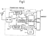
- a portable telephone for use in a digital cellular telephone system of the GSM standards, to which telephone the present invention is applied comprises an antenna 1 for transmitting a transmitting signal S11 to a base station (not shown), receiving a radio frequency signal from the base station and supplying it to a receiving portion 4 as a receiving signal S12.
- the telephone also comprises transceiver portion 10 for producing the transmitting signal S11 by frequency-converting and amplifying an input communications signal S14 and for converting the receiving signal S12 into a communications signal S18 and a handset 8 for producing the communications signal S14 and receiving the communications signal S18.
- control signals S20a and S20b are exchanged between the transceiver portion 10 and the handset 8 for call connection.
- the transceiver portion 10 further comprises a RF switch 2 of SPDT type having a common terminal connected to the antenna 1, a transmitting portion 3 responsive to the control signal S15 and to the communication signal S14 from the handset 8 to produce the transmitting signal S11 and sending the signal S11 through a first switch terminal of the RF switch 2 to the antenna 1.
- the receiving portion 4 receives the receiving signal S12 supplied from the antenna 1 through a second switch terminal of the RF switch 2, producing a control signal S17b and supplying a communications signal S18 to the handset 8.
- a PLL frequency synthesizer 5 supplies a local oscillating signal S13 to the transmitting portion 3 and to the receiving portion 4 in response to a frequency control signal S16a.
- a control portion 6 controls the transmitting portion 4, the receiving portion 4, the PLL frequency synthesizer 5 and the handset 8 by sending to them the control signals S15, S17a, S16a and S20a, respectively. Based on the signals S20b and S17b, the control portion 6 controls a frequency selection between the transmitting signal S11 and the receiving signal S12, an ON/OFF control of a transmitting carrier and a call connection to the base station.
- the transceiver portion 10 further comprises an LCD (liquid crystal display) portion 7 for visually displaying various indications including abnormality of operation of the transceiver 10, according to an instruction of a control signal S19 from the control portion 6.
- the transceiver portion 10 includes, in addition to the circuits shown, other components such as a power source package, these components are not shown since they are out of the present invention.
- the PLL frequency synthesizer 5 shown in Fig. 1 supplies an unlock alarm detected by an unlock alarm generating means included therein to the control portion 6 in the form of a control signal S16b.
- the control portion 6 processes various signals including abnormality alarms from other circuits and supplies a control signal S19 to the LCD portion 7 to display alarm conditions.
- the PLL frequency synthesizer 5 responds to the frequency control signal S16a from the control portion 6 to switch a frequency and prohibits a transmission of the unlock alarm (control signal S16b) during a transient time until a phase locked state is recovered under control of an unlock alarm prohibition means to be described later. Therefore, during the transient time, there is no unlock alarm signal supplied to the control portion 6, so that an erroneous unlock alarm is not displayed on the LCD portion 7.
- a frequency hopping operation in the transceiver portion shown in Fig. 1 will be described with reference to Fig. 1 as well as Fig 2.
- the transceiver portion 10 can use, in a service cell belonging to a current position of a vehicle mounting the transceiver portion 10, channels c0, c1 and c2 as a downlink frequency channel from the base station and the same channels c0, c1 and c2 as an uplink frequency channels to the base station.
- the unlink frequency and the downlink frequency are different even though the same frequency channel may be used therefor.
- Frequency channels d0 and e0 for a plurality of adjacent cells are displayed as monitor channels for monitoring field intensity.
- a switching sequence between the transmitting frequency channel and the receiving frequency channel that is, a frequency hopping sequence, is sent from the base station through the control channels (the receiving signal S12 of the receiving portion 4 and the control signal S17b) to the control portion 6 prior to an opening of a communications channel and the control portion 6 stores the frequency hopping sequence.
- the receiving signal S12 is supplied from the base station through the third burst of the c0 channel of the downlink to the receiving portion 3 (RX1). Then, the transmitting portion 4 sends the transmitting signal S11 through the same channel, the same frame and the same burst of the uplink (TX2).
- a burst of the uplink is set such that it is delayed from a corresponding burst of the downlink by a period corresponding to three bursts.
- the receiving portion 3 monitors the wield intensity of the d0 channel of the adjacent cell through the receiving signal S12 at a proper time during 5 bursts period until a communications burst (RX2) of a subsequent frame (Monitor1). After the monitoring of the adjacent cell, the receiving portion 3 receives the receiving signal S12 in the same third burst while frequency is hopped to the channel c2 (RX2). Then, the transmitting portion 4 sends the transmitting signal S11 is the third burst of the same c2 channel (TX2). A subsequent monitoring of field intensity of adjacent cell is performed by monitoring the e0 channel of another cell (Monitor2).
- the above-mentioned frequency hopping sequence is performed by switching frequency of the local oscillating signal S13 supplied from the PLL frequency synthesizer 5 under control of the frequency control signal S16a supplied from the control portion 6. Therefore, the frequency of local oscillating signal S13 supplied from the PLL frequency synthesizer 5 to the transmitting portion 3 and the receiving portion 4 has to be switched every transmitting and receiving burst.
- the PLL frequency synthesizer 5 which performs such frequency hopping performs a high-speed, highly frequent frequency switching of the local oscillating signal S13 at least once in 1 frame period.
- the transceiver 10 performs a transmitting or receiving operation only during a period corresponding to 3 bursts of 8 bursts constituting 1 frame and is in a waiting state during the remaining burst period.
- the PLL frequency synthesizer 5 becomes unlocked in every transient time immediately after each frequency switching of the local oscillating signal S13. Such unlock is inevitable even if the PLL synthesizer 5 operates normally. Thus, the PLL frequency synthesizer 5 performs the frequency switching during the waiting period of the transceiver 10 to prohibit a generation of unlock alarm for phase unlock during the transient period.
- the control signal S16a instructing the PLL synthesizer 5 to perform the frequency switching is composed of a dividing data signal S37 for assigning a frequency of the local oscillating signal and a strobe signal S38 for activating the signal S37.
- the dividing data signal S37 is supplied from the control portion 6 simultaneously with a start of burst transmission of the transmitting portion 3 and a start of a burst receiving of the receiving portion 4 and the strobe signal S38 is supplied after the above burst transmission and burst receiving complete.
- the PLL frequency synthesizer 5 responds to the strobe signal S38 to start the frequency switching of the local oscillating signal S13 and is phase unlocked during a transient time determined by a performance thereof.
- the PLL synthesizer 5 operates to recover the phase locked state till a subsequent burst transmission of burst receiving, that is, during the waiting period of the transceiver 10 which corresponds to one burst period or 1.5 burst period and produces the local oscillating signal S13 having a predetermined frequency.
- the unlock alarm prohibition means prohibits alarm generation over a period T starting from a time point at which the strobe signal S38 is supplied to the PLL synthesizer 5 and ending at an end of a certain tolerance time after the phase lock state is recovered.
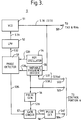
- the PLL synthesizer 5 comprises a PLL composed of a voltage-controlled oscillator 51 responsive to a control voltage S31 to supply a local oscillating signal S36 having a predetermined frequency to a synthesizer output terminal 501.
- a variable frequency divider 55 frequency-divides the signal S36 to produce a comparative signal S34 under control of a dividing data signal S37 supplied from a dividing data input terminal 502 for instructing a dividing ratio and a strobe signal supplied from a strobe signal input terminal 503 for activating the dividing data signal S37.
- a reference oscillator 54 supplies a reference signal S33 having a reference frequency to a phase detector 53 which compares in phase, the comparative signal S34 with the reference signal S33 to produce a phase difference signal S32.
- a low pass filter 52 integrates the phase difference signal S32 to produce the above-mentioned control voltage S31.
- the local oscillating signal S13 supplied from the PLL synthesizer 5 in Fig. 1 corresponds to the frequency signal S36 and the frequency control signal S16a for controlling the frequency of the local oscillating signal S13 is divided to the dividing data signal S37 and the strobe signal S38.
- the phase detector 53 in Fig. 3 When the PLL synthesizer 5 is in unlock state where there is the phase difference between the comparative signal S34 and the reference signal S33, the phase detector 53 in Fig. 3 outputs the phase difference signal S32 as well as a pulse phase difference detection signal S35 corresponding to the phase difference.
- the pulse phase difference detection signal S35 is supplied to a gate circuit 57 which produces an output signal S40 whose waveform is the same as that of the signal S35 when it is in an ON state and is zero potential when it is in an OFF state.
- the output pulse signal S40 is supplied to a pulse detection circuit 58 for converting an alarm of the PLL synthesizer 5 into an alarm output S41 and the pulse detection circuit 58 produces at an alarm terminal 504 of the control portion 6 in Fig. 1 the alarm output S41 as one of device alarms.
- a pulse generator circuit 56 (Fig. 3) composed of a one-shot multivibrator, etc., responds to the strobe signal S38 such as a trigger pulse to produce a gate pulse signal S39 having a constant duration T.
- the gate circuit 57 is turned OFF. Therefore, the pulse detection circuit 58 does not produce the alarm output S41 to the alarm output terminal 504 during a time period T starting at the supply of the strobe signal S38 thereto.
- the above-mentioned circuit constitutes the unlock alarm prohibition means described with respect to Fig. 1.
- the PLL synthesizer 5 shown in Fig. 3 switches the frequency of the frequency signal S36 every input of the dividing data signal S37 and the strobe signal S38 and becomes unlocked in every transient time immediately after each frequency switching of the local oscillating signal S13 even if the PLL synthesizer 5 operates normally. During the unlocked period, however, the generation of unlock alarm (alarm output S41) is prohibited by the unlock alarm prohibition means composed of the pulse generator circuit 56 and the gate circuit 57.
- the PLL synthesizer 5 does not send any alarm for an unlocking when it operates normally and thus a determination of abnormality is facilitated.
- the PLL synthesizer 5 As the local oscillator of the transceiver shown in Fig. 1 which has the frequency hopping function, there is no generation of erroneous unlock alarm even if a high-speed, highly frequent switching of frequency is performed.
- the latter circuit comprises an field-effect transistor (FET) TR1 having a gate used as the input terminal for the output pulse signal S40 and a source grounded, a diode DI having a cathode connected to a drain of the FET transistor TR1 and an anode connected to the alarm output terminal 504, a capacitor C1 connected between the anode of diode DI and ground and a resistor R1 connected between the anode of diode D1 and a positive source Vcc.
- FET field-effect transistor
- the pulse detection circuit 58 makes the voltage (alarm output S21) at the alarm output terminal 504 high with a predetermined time constant when the output pulse signal S40 is not supplied and makes it low immediately when the output pulse signal is detected, the low level signal being the unlock alarm indicative of the PLL synthesizer 5 unlocked.
- the reference oscillator 54 supplies the reference signal S33 having rectangular waveform.
- the frequency divider 55 supplies the comparative signal S38 which is a division of the frequency signal S36 (not shown).
- the strobe signal S38 is supplies to the variable frequency divider 55 at a time instance t2
- the signal S38 activates the dividing data signal S37 (not shown) which has been input thereto, to thereby change the dividing ratio of the variable frequency divider 55.
- the frequency of the comparative signal S34 the PLL synthesizer 5 becomes unlocked and thus there is provided a phase difference between the reference signal S33 and the comparative signal S34.
- the phase difference detection signal S35 in the form of pulse is generated correspondingly to the phase difference between the signals S33 and S34.
- the phase difference detection signal S35 is indicative of the unlocked state of the PLL synthesizer 5.
- unlock is inevitably produced in the initial state of the frequency switching of the frequency signal S36, the operation of the PLL synthesizer 5 is normal. Such unlock state continues till a time instance t3 which is determined by the performance of the PLL synthesizer 5.
- the pulse generator circuit 56 shown in Fig. 3 responds to the strobe signal S38 to produce the gate pulse signal S39 whose duration T corresponds to a time period which is a sum of the unlock time starting from the end (time instance t2) of the frequency switching of the PLL synthesizer 5 and ending at a time instance t3 and a certain constant tolerance time starting at the time instance t3 and ending at a time instance t4. That is, a leading edge of the gate pulse signal S39 coincide with a leading edge (t2) of the strobe signal S38 and a trailing edge thereof coincides with the time instance t4 after the time period T from the time instance t2.
- the output pulse signal S40 of the gate circuit 57 is always at a low level even if there is provided the phase difference detection signal S35 immediately after the frequency switching of the frequency signal S36. Therefore, the alarm output S41 of the pulse detection circuit 58 is always at a high level, causing the PLL synthesizer 5 to not send any alarm.
- the phase detector 53 compares phases of the supplied reference signal S33 and the comparative signal S34 on the bases of the trailing edges thereof and provides the phase difference detection signal S35 and the phase difference signal S32.
- the phase detector 53 which receives the reference signal S33 and the comparative signal S34 and provides the phase difference signal S32 and the phase difference detection signal S35, which are shown in Figs. 5 and 6, is integrated in a portion of an LSI for frequency synthesizer, such is ⁇ PC2833C (manufactured by NEC Corporation, Tokyo, Japan) and capable of comparing the phase of signal having frequency up to at least 1 MHz.
- Fig. 3 shows signal waveforms related to unlock alarm during an abnormal operation of the PLL synthesizer 5 where there is unlock state generated outside the frequency switching period of the frequency signal S36.
- the phase detector 53 produces the phase difference detection signal S35 at time instances t1, t5, t6 and t7 in a time period outside of the normal initial unlock period T from t2 to t4 of the PLL synthesizer 5. Therefore, the PLL synthesizer 5 is operating abnormally. Since the pulse generator circuit 56 opens the gate circuit 57 in a time other than the period T during which the gate pulse S39 is produced in response to the strobe signal S38, it outputs the phase difference detection signals S35 at the time instances t1, t5, t6 and t7 as the output pulse signal S40. When the output pulse signal S40 is supplied to the pulse detection circuit 58, the alarm output S41 produced at the alarm output terminal 504 immediately becomes a low level, indicating an alarm generating state of the PLL synthesizer 5.
- the PLL synthesizer according to the present invention when applied to a transceiver, prohibits sending of unlock alarm during the initial unlock seriod immediately after the frequency switching. Therefore, according to the present invention, in a transceiver in which a transmitting signal frequency and a receiving signal frequency are switched at high-speed highly frequently so that it is adaptable to the TDMA communication system with frequency hopping, it is possible to prohibit generation of any unlock alarm during a normal unlock period immediately after a frequency switching of a PLL synthesizer and thus it is possible to distinguish between true unlock state and the normal unlock state, eliminating any obstacle to a communication.
Abstract
Description
- The present invention relates to a radio transmitter/ receiver (referred to as "transceiver", hereinafter) having an unlock alarm of a frequency synthesizer including a PLL (phase locked loop) as one of device alarms and, particularly, to such a transceiver suitable for use in a radio communication system such as a time division multiple access (TDMA) communications system which requires high-speed and frequent switching between a receiving state and a transmitting state.
- The TDMA communications system is employed in many radio communications systems including a digital cellular telephone system according to Groupe Speciale Mobile (GSM) standard. In such a transceiver of the TDMA communications system, a single PLL frequency synthesizer is shared by a receiving portion and a transmitting portion of the transceiver as a local frequency source, since there is no simultaneous transmission and receiving. In such a digital cellular telephone system which requires highly precise frequency setting and reduction of size, the shared use of the PLL frequency synthesizer is unavoidable. Further, in the TDMA communications system such as a digital cellular telephone system, it is necessary, in order to maintain a quality of communication high, to switch transmitting and receiving frequencies, that is, to perform a frequency hopping in order to satisfy this requirement, the PLL frequency synthesizer constituting the local frequency signal source should be durable against high-speed, highly frequent frequency switching.
- In order to operate the PLL frequency synthesizer normally, the PLL frequency synthesizer must be kept phase locked. Therefore, any out-of-phase condition, that is, unlock condition must be detected and corrected quickly. To this end, the PLL frequency synthesizer usually includes an unlock detection circuit for detecting the unlock condition. On the other hand, a PLL frequency synthesizer to be used in a transceiver performing the frequency hopping usually becomes unlocked immediately after every frequency switching, producing an unlock alarm which is decided by the transceiver as an abnormal operation. Since such initial unlock occurs in the PLL frequency synthesizer so long as the associated transceiver performs the frequency hooping, it is impossible to distinguish an unlock which is caused by abnormality and is to be corrected from such initial unlock which occurs in a normal operation of the device.
- Therefore, an object of the present invention is to provide a transceiver of such as a TDMA communications system which requires a frequent switching of a transmitting signal and receiving signal and whose transmitting and receiving portions share a single PLL frequency synthesizer as their local frequency signal sources, in which any unlock alarm is not produced for a predetermined time period immediately after a frequency switching even if there is unlock condition of the PLL frequency synthesizer within the time period.
- Another object of the present invention is to provide a PLL frequency synthesizer in which a production of unlock alarm is prevented within a predetermined time period immediately after the frequency switching.
- A DLL frequency synthesizer which features the present invention is suitable to use in a transceiver of a communications system such as a TDMA communications system, in which timings of a transmission and receiving are inconsistent and high-speed and frequent switching of frequency between the transmission and receiving is required.
- The PLL synthesizer comprises a frequency divider for dividing an output of a voltage controlled oscillator (VCO), a phase detector for comparing an output of the frequency divider as a comparison signal with a reference signal from a reference oscillator to produce a phase difference signal and a PLL oscillator for controlling an oscillation frequency of the VCO according to the phase difference signal. The frequency switching of the PLL frequency synthesizer is started upon an application of a frequency control signal indicating a change of frequency dividing data to the frequency divider. The phase detector produces not only the phase difference signal but also a phase difference detection signal corresponding to the phase difference signal, when there is such phase difference, that is, it is in an unlock state. In response to the phase difference detection signal, an audible and/or visible alarm is displayed on an alarm display portion of the transceiver. The PLL frequency synthesizer according to the present invention includes an unlock alarm prohibition circuit for prohibiting a response of the alarm display portion to the phase difference detection signal for a predetermined time period from a start of the detection signal.
- An output frequency of the PLL frequency synthesizer is switched every supply of a dividing data signal and a strobe signal following the dividing data signal and there is produced a very brief phase unlock state in a transient time immediately after every frequency switching. However, the unlock alarm prohibition circuit prohibits production of unlock alarm in at least this transient time. Therefore, when the PLL frequency synthesizer according to the present invention is used in a transceiver having high frequency switching rate, the problem that unlock alarm is produced every signal frequency switching can be solved.
- The above-mentioned and other objects, features and advantages of the present invention will become more apparent from the following detailed description when taken in conjunction with the accompanying drawings, wherein:
- Fig 1 is a block diagram of an example of a TDMA communication transceiver adopting the GSM standards to which transceiver the present invention is applied;
- Fig. 2 is a timing chart illustrating a frequency hopping operation of the transceiver shown in Fig. 1;
- Fig. 3 is a block diagram of a PLL frequency synthesizer constituting a portion of the transceiver shown in Fig 1;
- Fig 4 is a circuit diagram of a pulse detection circuit constituting a portion of the PLL frequency synthesizer shown in Fig. 3;
- Fig. 5 shows signal waveforms during a normal operation of the PLL frequency synthesizer shown in Fig. 3; and
- Fig. 6 shows signal waveforms during an abnormal operation of the PLL frequency synthesizer shown in Fig 3.
- Referring to Fig 1, a portable telephone for use in a digital cellular telephone system of the GSM standards, to which telephone the present invention is applied comprises an
antenna 1 for transmitting a transmitting signal S11 to a base station (not shown), receiving a radio frequency signal from the base station and supplying it to a receivingportion 4 as a receiving signal S12. The telephone also comprisestransceiver portion 10 for producing the transmitting signal S11 by frequency-converting and amplifying an input communications signal S14 and for converting the receiving signal S12 into a communications signal S18 and ahandset 8 for producing the communications signal S14 and receiving the communications signal S18. It should be noted that control signals S20a and S20b are exchanged between thetransceiver portion 10 and thehandset 8 for call connection. - The
transceiver portion 10 further comprises aRF switch 2 of SPDT type having a common terminal connected to theantenna 1, a transmittingportion 3 responsive to the control signal S15 and to the communication signal S14 from thehandset 8 to produce the transmitting signal S11 and sending the signal S11 through a first switch terminal of theRF switch 2 to theantenna 1. Thereceiving portion 4 receives the receiving signal S12 supplied from theantenna 1 through a second switch terminal of theRF switch 2, producing a control signal S17b and supplying a communications signal S18 to thehandset 8. APLL frequency synthesizer 5 supplies a local oscillating signal S13 to the transmittingportion 3 and to the receivingportion 4 in response to a frequency control signal S16a. Acontrol portion 6 controls the transmittingportion 4, thereceiving portion 4, thePLL frequency synthesizer 5 and thehandset 8 by sending to them the control signals S15, S17a, S16a and S20a, respectively. Based on the signals S20b and S17b, thecontrol portion 6 controls a frequency selection between the transmitting signal S11 and the receiving signal S12, an ON/OFF control of a transmitting carrier and a call connection to the base station. Thetransceiver portion 10 further comprises an LCD (liquid crystal display)portion 7 for visually displaying various indications including abnormality of operation of thetransceiver 10, according to an instruction of a control signal S19 from thecontrol portion 6. Although thetransceiver portion 10 includes, in addition to the circuits shown, other components such as a power source package, these components are not shown since they are out of the present invention. - The
PLL frequency synthesizer 5 shown in Fig. 1 supplies an unlock alarm detected by an unlock alarm generating means included therein to thecontrol portion 6 in the form of a control signal S16b. Thecontrol portion 6 processes various signals including abnormality alarms from other circuits and supplies a control signal S19 to theLCD portion 7 to display alarm conditions. On the contrary, thePLL frequency synthesizer 5 responds to the frequency control signal S16a from thecontrol portion 6 to switch a frequency and prohibits a transmission of the unlock alarm (control signal S16b) during a transient time until a phase locked state is recovered under control of an unlock alarm prohibition means to be described later. Therefore, during the transient time, there is no unlock alarm signal supplied to thecontrol portion 6, so that an erroneous unlock alarm is not displayed on theLCD portion 7. - A frequency hopping operation in the transceiver portion shown in Fig. 1 will be described with reference to Fig. 1 as well as Fig 2. Describing, first, a TDMA signal, it is assumed that the
transceiver portion 10 can use, in a service cell belonging to a current position of a vehicle mounting thetransceiver portion 10, channels c0, c1 and c2 as a downlink frequency channel from the base station and the same channels c0, c1 and c2 as an uplink frequency channels to the base station. It should be noted that the unlink frequency and the downlink frequency are different even though the same frequency channel may be used therefor. Frequency channels d0 and e0 for a plurality of adjacent cells are displayed as monitor channels for monitoring field intensity. A switching sequence between the transmitting frequency channel and the receiving frequency channel, that is, a frequency hopping sequence, is sent from the base station through the control channels (the receiving signal S12 of the receivingportion 4 and the control signal S17b) to thecontrol portion 6 prior to an opening of a communications channel and thecontrol portion 6 stores the frequency hopping sequence. According to the GSM standards, one TDMA frame (1 frame = 4.615 ms) is composed of 8 bursts (1 burst = 0.577 ms). - First, the receiving signal S12 is supplied from the base station through the third burst of the c0 channel of the downlink to the receiving portion 3 (RX1). Then, the transmitting
portion 4 sends the transmitting signal S11 through the same channel, the same frame and the same burst of the uplink (TX2). A burst of the uplink is set such that it is delayed from a corresponding burst of the downlink by a period corresponding to three bursts. Then, in order to check whether there is any adjacent cell in which it may be possible to obtain a better communications quality than in the present service cell in which the telephone currently exists, thereceiving portion 3 monitors the wield intensity of the d0 channel of the adjacent cell through the receiving signal S12 at a proper time during 5 bursts period until a communications burst (RX2) of a subsequent frame (Monitor1). After the monitoring of the adjacent cell, thereceiving portion 3 receives the receiving signal S12 in the same third burst while frequency is hopped to the channel c2 (RX2). Then, the transmittingportion 4 sends the transmitting signal S11 is the third burst of the same c2 channel (TX2). A subsequent monitoring of field intensity of adjacent cell is performed by monitoring the e0 channel of another cell (Monitor2). - The above-mentioned frequency hopping sequence is performed by switching frequency of the local oscillating signal S13 supplied from the
PLL frequency synthesizer 5 under control of the frequency control signal S16a supplied from thecontrol portion 6. Therefore, the frequency of local oscillating signal S13 supplied from thePLL frequency synthesizer 5 to the transmittingportion 3 and the receivingportion 4 has to be switched every transmitting and receiving burst. ThePLL frequency synthesizer 5 which performs such frequency hopping performs a high-speed, highly frequent frequency switching of the local oscillating signal S13 at least once in 1 frame period. Thetransceiver 10 performs a transmitting or receiving operation only during a period corresponding to 3 bursts of 8 bursts constituting 1 frame and is in a waiting state during the remaining burst period. - In Fig. 3, the
PLL frequency synthesizer 5 becomes unlocked in every transient time immediately after each frequency switching of the local oscillating signal S13. Such unlock is inevitable even if thePLL synthesizer 5 operates normally. Thus, thePLL frequency synthesizer 5 performs the frequency switching during the waiting period of thetransceiver 10 to prohibit a generation of unlock alarm for phase unlock during the transient period. the control signal S16a instructing thePLL synthesizer 5 to perform the frequency switching is composed of a dividing data signal S37 for assigning a frequency of the local oscillating signal and a strobe signal S38 for activating the signal S37. The dividing data signal S37 is supplied from thecontrol portion 6 simultaneously with a start of burst transmission of the transmittingportion 3 and a start of a burst receiving of the receivingportion 4 and the strobe signal S38 is supplied after the above burst transmission and burst receiving complete. ThePLL frequency synthesizer 5 responds to the strobe signal S38 to start the frequency switching of the local oscillating signal S13 and is phase unlocked during a transient time determined by a performance thereof. ThePLL synthesizer 5 operates to recover the phase locked state till a subsequent burst transmission of burst receiving, that is, during the waiting period of thetransceiver 10 which corresponds to one burst period or 1.5 burst period and produces the local oscillating signal S13 having a predetermined frequency. On the other hand, the unlock alarm prohibition means prohibits alarm generation over a period T starting from a time point at which the strobe signal S38 is supplied to thePLL synthesizer 5 and ending at an end of a certain tolerance time after the phase lock state is recovered. - The
PLL synthesizer 5 comprises a PLL composed of a voltage-controlledoscillator 51 responsive to a control voltage S31 to supply a local oscillating signal S36 having a predetermined frequency to asynthesizer output terminal 501. Avariable frequency divider 55 frequency-divides the signal S36 to produce a comparative signal S34 under control of a dividing data signal S37 supplied from a dividingdata input terminal 502 for instructing a dividing ratio and a strobe signal supplied from a strobesignal input terminal 503 for activating the dividing data signal S37. Areference oscillator 54 supplies a reference signal S33 having a reference frequency to aphase detector 53 which compares in phase, the comparative signal S34 with the reference signal S33 to produce a phase difference signal S32. Alow pass filter 52 integrates the phase difference signal S32 to produce the above-mentioned control voltage S31. The local oscillating signal S13 supplied from thePLL synthesizer 5 in Fig. 1 corresponds to the frequency signal S36 and the frequency control signal S16a for controlling the frequency of the local oscillating signal S13 is divided to the dividing data signal S37 and the strobe signal S38. - When the
PLL synthesizer 5 is in unlock state where there is the phase difference between the comparative signal S34 and the reference signal S33, thephase detector 53 in Fig. 3 outputs the phase difference signal S32 as well as a pulse phase difference detection signal S35 corresponding to the phase difference. The pulse phase difference detection signal S35 is supplied to agate circuit 57 which produces an output signal S40 whose waveform is the same as that of the signal S35 when it is in an ON state and is zero potential when it is in an OFF state. The output pulse signal S40 is supplied to apulse detection circuit 58 for converting an alarm of thePLL synthesizer 5 into an alarm output S41 and thepulse detection circuit 58 produces at analarm terminal 504 of thecontrol portion 6 in Fig. 1 the alarm output S41 as one of device alarms. - A pulse generator circuit 56 (Fig. 3) composed of a one-shot multivibrator, etc., responds to the strobe signal S38 such as a trigger pulse to produce a gate pulse signal S39 having a constant duration T. Upon the signal S39, the
gate circuit 57 is turned OFF. Therefore, thepulse detection circuit 58 does not produce the alarm output S41 to thealarm output terminal 504 during a time period T starting at the supply of the strobe signal S38 thereto. The above-mentioned circuit constitutes the unlock alarm prohibition means described with respect to Fig. 1. - The
PLL synthesizer 5 shown in Fig. 3 switches the frequency of the frequency signal S36 every input of the dividing data signal S37 and the strobe signal S38 and becomes unlocked in every transient time immediately after each frequency switching of the local oscillating signal S13 even if thePLL synthesizer 5 operates normally. During the unlocked period, however, the generation of unlock alarm (alarm output S41) is prohibited by the unlock alarm prohibition means composed of thepulse generator circuit 56 and thegate circuit 57. - Therefore, the
PLL synthesizer 5 does not send any alarm for an unlocking when it operates normally and thus a determination of abnormality is facilitated. By using thePLL synthesizer 5 as the local oscillator of the transceiver shown in Fig. 1 which has the frequency hopping function, there is no generation of erroneous unlock alarm even if a high-speed, highly frequent switching of frequency is performed. - Referring to Fig. 4 which shows an example of circuit construction of the
pulse detection circuit 58 shown in Fig. 3, the latter circuit comprises an field-effect transistor (FET) TR1 having a gate used as the input terminal for the output pulse signal S40 and a source grounded, a diode DI having a cathode connected to a drain of the FET transistor TR1 and an anode connected to thealarm output terminal 504, a capacitor C1 connected between the anode of diode DI and ground and a resistor R1 connected between the anode of diode D1 and a positive source Vcc. Thepulse detection circuit 58 makes the voltage (alarm output S21) at thealarm output terminal 504 high with a predetermined time constant when the output pulse signal S40 is not supplied and makes it low immediately when the output pulse signal is detected, the low level signal being the unlock alarm indicative of thePLL synthesizer 5 unlocked. - Referring to Fig. 3 as well as Fig 5 showing some signal waveforms related to the unlock alarm in a normal operation of the
PLL synthesizer 5, thereference oscillator 54 supplies the reference signal S33 having rectangular waveform. Thefrequency divider 55 supplies the comparative signal S38 which is a division of the frequency signal S36 (not shown). When the strobe signal S38 is supplies to thevariable frequency divider 55 at a time instance t2, the signal S38 activates the dividing data signal S37 (not shown) which has been input thereto, to thereby change the dividing ratio of thevariable frequency divider 55. Thus, the frequency of the comparative signal S34, thePLL synthesizer 5 becomes unlocked and thus there is provided a phase difference between the reference signal S33 and the comparative signal S34. As a result, the phase difference detection signal S35 in the form of pulse is generated correspondingly to the phase difference between the signals S33 and S34. The phase difference detection signal S35 is indicative of the unlocked state of thePLL synthesizer 5. However, since such unlock is inevitably produced in the initial state of the frequency switching of the frequency signal S36, the operation of thePLL synthesizer 5 is normal. Such unlock state continues till a time instance t3 which is determined by the performance of thePLL synthesizer 5. - On the other hand, the
pulse generator circuit 56 shown in Fig. 3 responds to the strobe signal S38 to produce the gate pulse signal S39 whose duration T corresponds to a time period which is a sum of the unlock time starting from the end (time instance t2) of the frequency switching of thePLL synthesizer 5 and ending at a time instance t3 and a certain constant tolerance time starting at the time instance t3 and ending at a time instance t4. That is, a leading edge of the gate pulse signal S39 coincide with a leading edge (t2) of the strobe signal S38 and a trailing edge thereof coincides with the time instance t4 after the time period T from the time instance t2. Thus, when thePLL synthesizer 5 operates normally, the output pulse signal S40 of thegate circuit 57 is always at a low level even if there is provided the phase difference detection signal S35 immediately after the frequency switching of the frequency signal S36. Therefore, the alarm output S41 of thepulse detection circuit 58 is always at a high level, causing thePLL synthesizer 5 to not send any alarm. - The
phase detector 53 compares phases of the supplied reference signal S33 and the comparative signal S34 on the bases of the trailing edges thereof and provides the phase difference detection signal S35 and the phase difference signal S32. Thephase detector 53 which receives the reference signal S33 and the comparative signal S34 and provides the phase difference signal S32 and the phase difference detection signal S35, which are shown in Figs. 5 and 6, is integrated in a portion of an LSI for frequency synthesizer, such is µPC2833C (manufactured by NEC Corporation, Tokyo, Japan) and capable of comparing the phase of signal having frequency up to at least 1 MHz. - A reference is made to Fig. 3 as well as Fig. 6 which shows signal waveforms related to unlock alarm during an abnormal operation of the
PLL synthesizer 5 where there is unlock state generated outside the frequency switching period of the frequency signal S36. - The
phase detector 53 produces the phase difference detection signal S35 at time instances t1, t5, t6 and t7 in a time period outside of the normal initial unlock period T from t2 to t4 of thePLL synthesizer 5. Therefore, thePLL synthesizer 5 is operating abnormally. Since thepulse generator circuit 56 opens thegate circuit 57 in a time other than the period T during which the gate pulse S39 is produced in response to the strobe signal S38, it outputs the phase difference detection signals S35 at the time instances t1, t5, t6 and t7 as the output pulse signal S40. When the output pulse signal S40 is supplied to thepulse detection circuit 58, the alarm output S41 produced at thealarm output terminal 504 immediately becomes a low level, indicating an alarm generating state of thePLL synthesizer 5. - As described hereinbefore, the PLL synthesizer according to the present invention, when applied to a transceiver, prohibits sending of unlock alarm during the initial unlock seriod immediately after the frequency switching. Therefore, according to the present invention, in a transceiver in which a transmitting signal frequency and a receiving signal frequency are switched at high-speed highly frequently so that it is adaptable to the TDMA communication system with frequency hopping, it is possible to prohibit generation of any unlock alarm during a normal unlock period immediately after a frequency switching of a PLL synthesizer and thus it is possible to distinguish between true unlock state and the normal unlock state, eliminating any obstacle to a communication.
- Although the present invention has been described with reference to the specific embodiment, this description is not meant to be construed in a limiting sense. Various modifications of the disclosed embodiments, as well as other embodiments of the present invention, will become apparent to persons skilled in the art upon reference to the description of the present invention. It is, therefore, contemplated that the appended claims will cover any modifications or embodiments as fall within the true scope of the present invention.
Claims (18)
- A radio transceiver comprising:
transmitting means for transmitting a first radio frequency carrier modulated with an information signal;
receiving means for receiving a second radio frequency carrier modulated with an information signal;
PLL frequency synthesizer means including a phase locked loop for supplying local oscillating signals having frequencies related in a predetermined manner to said first frequency and said second frequency to said transmitting means and said receiving means;
alarm display means responsive to a display control signal for displaying a device alarm;
frequency control means for controlling said transmitting means, said receiving means and said PLL synthesizer such that frequencies of said first radio frequency carrier and said second radio frequency carrier are switched; and
display control means for supplying said display control signal;
wherein said transmitting means and said receiving means are adaptable to TDMA system for transmitting and receiving said first radio frequency carrier and said second radio frequency carrier in the form of bursts by ON/OFF controlling of said first radio frequency carrier and said second radio frequency carrier;
and wherein said PLL frequency synthesizer comprises:
frequency switching means responsive to a frequency control signal from said frequency control means to switch a frequency of said local oscillating signal;
alarm generation means responsive to an unlock state of said phase locked loop to supply an alarm signal to said display control means; and
alarm prohibition means responsive to said frequency control means to prohibit said alarm generation means to generate said alarm signal during a predetermined time immediately after a frequency switching of said first radio frequency carrier and said second radio frequency carrier. - The transceiver claimed in claim 1, wherein said frequency control signal comprises:
a frequency assigning signal for assigning the frequency of said local oscillating signal; and
a strobe signal supplied after said frequency assigning signal to activate said frequency assigning signal. - The transceiver claimed in claim 2, wherein said prohibition of said alarm signal generation is started in response to said strobe signal.
- The transceiver claimed in claim 1, wherein said transceiver is of a radio transceiver of TDMA system capable of selectively setting a timing of making said first ratio frequency carried and said second radio frequency carrier in ON state and frequencies of said carriers, and wherein said predetermined time is shorter than a time during which said first radio frequency carrier and said second radio frequency carrier are not in said ON state.
- A radio transceiver including a transmitting means for transmitting a first radio frequency carrier modulated with an information signal to be transmitted through an antenna, a receiving means for receiving a second ratio frequency carrier modulated with an information signal to be received through said antenna, a PLL frequency synthesizer including a phase locked loop for supplying local oscillating signals having frequencies related in a predetermined manner to said first frequency and said second frequency to said transmitting means and said receiving means, alarm display means responsive to a display control signal for displaying a device alarm, frequency control means for controlling said transmitting means, said receiving means and said PLL synthesizer such that frequencies of said first radio frequency carrier and said second radio frequency carrier are switched and display control means for supplying said display control signal, said transceiver comprising:
said transmitting means and said receiving means being transceiver means adaptable to TDMA system for transmitting and receiving said first radio frequency carrier and said second radio frequency carrier in the form of bursts by ON/OFF controlling of said first radio frequency carrier and said second radio frequency carrier;
said PLL frequency synthesizer comprising:
a voltage controlled oscillator responsive to a control voltage to produce a local oscillating signal having an arbitrary frequency;
variable frequency divider means responsive to a dividing data signal from said frequency control means, said dividing data signal being indicative of a frequency dividing ratio, and a strobe signal for activating said dividing data signal to frequency-divide said local oscillating signal to thereby produce a comparative signal;
a reference oscillating means for producing a reference signal having a reference frequency;
phase detection means responsive to a phase difference between said comparative signal and said reference signal to produce a phase difference signal and a control signal;
low-pass filter means for integrating said control signal and supplying it to said voltage controlled oscillating means as said control voltage;
unlock alarm generation means for producing an unlock alarm from said phase difference signal; and
unlock alarm prohibition means for controlling said unlock alarm generation means to prohibit generation of said unlock alarm for a constant time. - The transceiver claimed in claim 5, wherein said prohibition of said alarm signal generation is started in response to said strobe signal.
- The transceiver claimed in claim 5, wherein said transceiver is of a radio transceiver of TDMA system capable of selectively setting a timing of making said first radio frequency carrier and said second radio frequency carrier in ON state and frequencies of said carriers, and wherein said predetermined time is shorter than a time during which said first radio frequency carrier and said second radio frequency carrier are not in said ON state.
- A radio transceiver including a transmitting means for transmitting a first radio frequency carrier modulated with an information signal to be transmitted through an antenna, a receiving means for receiving a second radio frequency carrier modulated high an information signal to be received through said antenna, a PLL frequency synthesizer including a phase locked loop for supplying local oscillating signals having frequencies related in a predetermined manner to said first frequency and said second frequency to said transmitting means and said receiving means, alarm display means responsive to a display control signal for displaving a device alarm, frequency control means for controlling said transmitting means, said receiving means and said PLL synthesizer such that frequencies of said first radio frequency carrier and said second radio frequency carrier are switched and display control means for supplying said display control signal, said transceiver comprising:
said transmitting means and said receiving means being transceiver means adaptable to TDMA system for transmitting and receiving said first radio frequency carrier and said second radio frequency carrier in the form of bursts by ON/OFF controlling of said first radio frequency carrier and said second radio frequency carrier;
said PLL frequency synthesizer comprising:
a voltage controlled oscillator responsive to a control voltage to produce a local oscillating signal having an arbitrary frequency;
variable frequency divider means responsive to a dividing data signal from said frequency control means, said dividing data signal being indicative of a frequency dividing ratio, and a strobe signal for activating said dividing data signal to frequency-divide said local oscillating signal to thereby produce a comparative signal;
a reference oscillating means for producing a reference signal having a reference frequency;
phase detection means responsive to a phase difference between said comparative signal and said reference signal to produce a phase difference signal and a control signal;
low-pass filter means for integrating said control signal and supplying it to said voltage controlled oscillating means as said control voltage;
pulse generator means responsive to said strobe signal to produce a gate pulse signal having a predetermined duration;
gate means responsive to said gate pulse signal to gate said phase difference signal to thereby produce an output signal; and
pulse detection means responsive to said output pulse signal to produce an unlock alarm signal. - The transceiver claimed in claim 8, wherein said unlock alarm signal produced by said pulse detection means takes in a high level with a predetermined time constant when said output pulse signal is not detected and changes it state to a low level immediately when said output pulse is detected.
- The transceiver claimed in claim 8, wherein said pulse detection means comprises:
an FET having a gate as an input terminal for said output pulse signal and a source connected to ground;
a diode having a cathode connected to a drain of said FET and an anode as an output terminal for said unlock alarm signal;
a capacitor connected between said anode of said diode and said ground; and
a resistor connected between a positive source and said anode of said diode. - A PLL frequency synthesizer including a phase locked loop and producing a high frequency output having a frequency variable according to a frequency control signal, said PLL synthesizer comprising:
unlock alarm generation means responsive to an unlocked state of said phase locked loop to produce an unlock alarm; and
unlock prohibition means for prohibiting generation of said unlock alarm for a predetermined time immediately after a frequency switching caused be said frequency control signal. - The PLL synthesizer claimed in claim 11, wherein said frequency control signal comprises:
a frequency assigning signal for assigning a frequency of said local oscillating signal; and
a strobe signal supplied after said frequency assigning signal to activate said frequency assigning signal. - The PTL synthesizer claimed in claim 12, wherein the prohibition of generation of said unlock alarm is started in response to said strobe signal.
- A PLL synthesizer comprising:
a voltage controlled oscillator responsive to a control voltage to produce a local oscillating signal having an arbitrary frequency;
variable frequency divider means responsive to a dividing data signal from said frequency control means, said dividing data signal being indicative of a frequency dividing ratio, and a strobe signal for activating said dividing data signal to frequency-divide said local oscillating signal to thereby produce a comparative signal;
a reference oscillating means for producing a reference signal having a reference frequency;
phase detection means responsive to a phase difference between said comparative signal and said reference signal to produce a phase difference signal and a control signal;
low-pass filter means for integrating said control signal and supplying it to said voltage controlled oscillating means as said control voltage;
unlock alarm generation means for producing an unlock alarm from said phase difference signal; and
unlock alarm prohibition means for controlling said unlock alarm generation means to prohibit generation of said unlock alarm for a constant time. - The PLL synthesizer claimed in claim 14, wherein the prohibition of generation of said unlock alarm is started in response to said strobe signal.
- A PLL synthesizer comprising:
a voltage controlled oscillator responsive to a control voltage to produce a local oscillating signal having an arbitrary frequency;
variable frequency divider means responsive to a dividing data signal from said frequency control means, said dividing data signal being indicative of a frequency dividing ratio, and a strobe signal for activating said dividing data signal to frequency-divide said local oscillating signal to thereby produce a comparative signal;
a reference oscillating means for producing a reference signal having a reference frequency;
phase detection means responsive to a phase difference between said comparative signal and said reference signal to produce a phase difference signal and a control signal;
low-pass filter means for integrating said control signal and supplying it to said voltage controlled oscillating means as said control voltage;
pulse generator means responsive to said strobe signal to produce a gate pulse signal having a predetermined duration;
gate means responsive to said gate pulse signal to produce an output pulse signal; and
pulse detection means responsive to said output pulse signal to produce an unlock alarm signal. - The PLL synthesizer claimed in claim 16, wherein said unlock alarm signal produced by said pulse detection means takes in a high level with a predetermined time constant when said output pulse signal is not detected and changes it state to a low level immediately when said output pulse is detected.
- The PLL synthesizer claimed in claim 17, wherein said pulse detection means comprises:
an FET having a gate as an input terminal for said output pulse signal and a source connected to ground;
a diode having a cathode connected to a drain of said FET and an anode as an output terminal for said unlock alarm signal;
a capacitor connected between said anode of said diode and said ground; and
a resistor connected between a positive source and said anode of said diode.
Applications Claiming Priority (2)
| Application Number | Priority Date | Filing Date | Title |
|---|---|---|---|
| JP29396390 | 1990-10-31 | ||
| JP293963/90 | 1990-10-31 |
Publications (3)
| Publication Number | Publication Date |
|---|---|
| EP0484158A2 true EP0484158A2 (en) | 1992-05-06 |
| EP0484158A3 EP0484158A3 (en) | 1992-09-23 |
| EP0484158B1 EP0484158B1 (en) | 1996-04-17 |
Family
ID=17801458
Family Applications (1)
| Application Number | Title | Priority Date | Filing Date |
|---|---|---|---|
| EP91310074A Expired - Lifetime EP0484158B1 (en) | 1990-10-31 | 1991-10-31 | Radio transceiver having PLL synthesizer |
Country Status (5)
| Country | Link |
|---|---|
| US (1) | US5319798A (en) |
| EP (1) | EP0484158B1 (en) |
| AU (1) | AU657280B2 (en) |
| CA (1) | CA2054599C (en) |
| DE (1) | DE69118813T2 (en) |
Cited By (4)
| Publication number | Priority date | Publication date | Assignee | Title |
|---|---|---|---|---|
| WO1996012348A1 (en) * | 1994-10-14 | 1996-04-25 | Nokia Telecommunications Oy | A lock alarm circuit for a frequency synthesizer |
| WO1996021987A2 (en) * | 1995-01-04 | 1996-07-18 | Nokia Telecommunications Oy | Radio system for cordless subscriber line interface |
| EP1261134A2 (en) * | 2001-04-25 | 2002-11-27 | Texas Instruments Incorporated | Digital phase locked loop |
| WO2004082145A1 (en) * | 2003-03-11 | 2004-09-23 | Fujitsu Limited | Phase-locked loop circuit |
Families Citing this family (19)
| Publication number | Priority date | Publication date | Assignee | Title |
|---|---|---|---|---|
| US5802447A (en) * | 1995-02-08 | 1998-09-01 | Casio Computer Co., Ltd. | Transmitter-receiver for a radio communication apparatus |
| WO1996037967A1 (en) * | 1995-05-26 | 1996-11-28 | Motorola Inc. | Selective call receiver having automatically adjusted impedance match for antenna |
| US5907545A (en) * | 1996-01-16 | 1999-05-25 | Canon Kk | Wireless communication apparatus and method |
| JPH09261106A (en) * | 1996-03-22 | 1997-10-03 | Matsushita Electric Ind Co Ltd | Mobile radio equipment operated for plural frequency bands |
| GB2313001B (en) * | 1996-05-07 | 2000-11-01 | Nokia Mobile Phones Ltd | Frequency modulation using a phase-locked loop |
| US5950115A (en) * | 1997-08-29 | 1999-09-07 | Adaptec, Inc. | GHz transceiver phase lock loop having autofrequency lock correction |
| US20030003887A1 (en) * | 1998-05-29 | 2003-01-02 | Lysander Lim | Radio-frequency communication apparatus and associated methods |
| US7035607B2 (en) * | 1998-05-29 | 2006-04-25 | Silicon Laboratories Inc. | Systems and methods for providing an adjustable reference signal to RF circuitry |
| US7221921B2 (en) * | 1998-05-29 | 2007-05-22 | Silicon Laboratories | Partitioning of radio-frequency apparatus |
| US7242912B2 (en) * | 1998-05-29 | 2007-07-10 | Silicon Laboratories Inc. | Partitioning of radio-frequency apparatus |
| JP2000341165A (en) * | 1999-05-25 | 2000-12-08 | Matsushita Electric Ind Co Ltd | Communication equipment, communication method and recording medium |
| EP1100243A3 (en) * | 1999-11-12 | 2004-03-17 | Sony Corporation | Telephone set, communication adaptor, home appliance control method, and program recording medium |
| US7792509B2 (en) * | 2002-01-07 | 2010-09-07 | St-Ericsson Sa | Transceiver with multi-state direct digital synthesizer driven phase locked loop |
| AU2003901650A0 (en) * | 2003-04-08 | 2003-05-01 | Standard Communications Pty Ltd | A radio beacon |
| JP4211621B2 (en) * | 2004-02-04 | 2009-01-21 | 双葉電子工業株式会社 | Model radio control system |
| US7747237B2 (en) * | 2004-04-09 | 2010-06-29 | Skyworks Solutions, Inc. | High agility frequency synthesizer phase-locked loop |
| KR100959333B1 (en) * | 2006-09-29 | 2010-05-20 | 삼성전자주식회사 | Apparatus for bidirectional communication using auxiliary band in wireless communication system |
| CN101841346B (en) * | 2009-03-19 | 2014-01-15 | 鸿富锦精密工业(深圳)有限公司 | Wireless transceiver |
| US20150092636A1 (en) * | 2013-09-30 | 2015-04-02 | Broadcom Corporation | Single local oscillator architecture |
Citations (4)
| Publication number | Priority date | Publication date | Assignee | Title |
|---|---|---|---|---|
| US3932821A (en) * | 1974-11-08 | 1976-01-13 | Narco Scientific Industries, Inc. | Out of lock detector for phase lock loop synthesizer |
| US4777655A (en) * | 1985-11-28 | 1988-10-11 | Hitachi, Ltd. | Control signal receiving system |
| EP0302562A1 (en) * | 1987-07-29 | 1989-02-08 | Philips Composants | Frequency synthesizer having a tuning indicator device |
| EP0380946A2 (en) * | 1989-01-31 | 1990-08-08 | Siemens Aktiengesellschaft | Method for the control of the regulation ability of a phase-locked loop circuit |
Family Cites Families (4)
| Publication number | Priority date | Publication date | Assignee | Title |
|---|---|---|---|---|
| US380946A (en) * | 1888-04-10 | Central station for alternate-current systems of electrical distribution | ||
| US3988696A (en) * | 1975-11-28 | 1976-10-26 | The Bendix Corporation | Phase lock detector for digital frequency synthesizer |
| US4499434A (en) * | 1982-07-19 | 1985-02-12 | Rockwell International Corporation | PLL Phase error alarm related to associated receiver |
| US5055802A (en) * | 1990-04-30 | 1991-10-08 | Motorola, Inc. | Multiaccumulator sigma-delta fractional-n synthesis |
-
1991
- 1991-10-31 EP EP91310074A patent/EP0484158B1/en not_active Expired - Lifetime
- 1991-10-31 DE DE69118813T patent/DE69118813T2/en not_active Expired - Fee Related
- 1991-10-31 US US07/785,548 patent/US5319798A/en not_active Expired - Fee Related
- 1991-10-31 AU AU86920/91A patent/AU657280B2/en not_active Ceased
- 1991-10-31 CA CA002054599A patent/CA2054599C/en not_active Expired - Fee Related
Patent Citations (4)
| Publication number | Priority date | Publication date | Assignee | Title |
|---|---|---|---|---|
| US3932821A (en) * | 1974-11-08 | 1976-01-13 | Narco Scientific Industries, Inc. | Out of lock detector for phase lock loop synthesizer |
| US4777655A (en) * | 1985-11-28 | 1988-10-11 | Hitachi, Ltd. | Control signal receiving system |
| EP0302562A1 (en) * | 1987-07-29 | 1989-02-08 | Philips Composants | Frequency synthesizer having a tuning indicator device |
| EP0380946A2 (en) * | 1989-01-31 | 1990-08-08 | Siemens Aktiengesellschaft | Method for the control of the regulation ability of a phase-locked loop circuit |
Non-Patent Citations (1)
| Title |
|---|
| 37th IEEE Vehicular Technology Confereence. 1-3 June, 1987. Florida. USA. p293-299. "Radio Test Performance of a Narrowband TDMA System". Stjernvall et al. * |
Cited By (13)
| Publication number | Priority date | Publication date | Assignee | Title |
|---|---|---|---|---|
| WO1996012348A1 (en) * | 1994-10-14 | 1996-04-25 | Nokia Telecommunications Oy | A lock alarm circuit for a frequency synthesizer |
| US5625326A (en) * | 1994-10-14 | 1997-04-29 | Nokia Telecommunications Oy | Lock alarm circuit of a synthesizer |
| AU699831B2 (en) * | 1994-10-14 | 1998-12-17 | Nokia Telecommunications Oy | A lock alarm circuit for a frequency synthesizer |
| CN1062397C (en) * | 1994-10-14 | 2001-02-21 | 诺基亚电信公司 | Lock alarm circuit for frequency synthesizer |
| WO1996021987A2 (en) * | 1995-01-04 | 1996-07-18 | Nokia Telecommunications Oy | Radio system for cordless subscriber line interface |
| WO1996021987A3 (en) * | 1995-01-04 | 1996-09-12 | Nokia Telecommunications Oy | Radio system for cordless subscriber line interface |
| EP1261134A2 (en) * | 2001-04-25 | 2002-11-27 | Texas Instruments Incorporated | Digital phase locked loop |
| EP1261134A3 (en) * | 2001-04-25 | 2004-11-24 | Texas Instruments Incorporated | Digital phase locked loop |
| US8385476B2 (en) | 2001-04-25 | 2013-02-26 | Texas Instruments Incorporated | Digital phase locked loop |
| US8742808B2 (en) | 2001-04-25 | 2014-06-03 | Texas Instruments Incorporated | Digital phase locked loop |
| US9893735B2 (en) | 2001-04-25 | 2018-02-13 | Texas Instruments Incorporated | Digital phase locked loop |
| WO2004082145A1 (en) * | 2003-03-11 | 2004-09-23 | Fujitsu Limited | Phase-locked loop circuit |
| US7440518B2 (en) | 2003-03-11 | 2008-10-21 | Fujitsu Limited | Phase-locked loop circuit |
Also Published As
| Publication number | Publication date |
|---|---|
| DE69118813T2 (en) | 1996-09-26 |
| EP0484158B1 (en) | 1996-04-17 |
| CA2054599A1 (en) | 1992-05-01 |
| CA2054599C (en) | 1996-02-20 |
| DE69118813D1 (en) | 1996-05-23 |
| EP0484158A3 (en) | 1992-09-23 |
| AU8692091A (en) | 1992-05-07 |
| AU657280B2 (en) | 1995-03-09 |
| US5319798A (en) | 1994-06-07 |
Similar Documents
| Publication | Publication Date | Title |
|---|---|---|
| US5319798A (en) | Radio transceiver having PLL synthesizer | |
| US5598405A (en) | Time division multiple access time division duplex type transmitter-receiver | |
| KR0165007B1 (en) | Phase loop lock synchronization circuit and method thereof | |
| US4521918A (en) | Battery saving frequency synthesizer arrangement | |
| US5521947A (en) | Phase detection reset in phase locked loops used for direct VCO modulation | |
| US5703539A (en) | Apparatus and method for controlling the loop bandwidth of a phase locked loop | |
| US5963100A (en) | Frequency synthesizer having a speed-up circuit | |
| US20070087716A1 (en) | Wireless communication system | |
| US5448763A (en) | Apparatus and method for operating a phase locked loop frequency synthesizer responsive to radio frequency channel spacing | |
| EP0984648B1 (en) | Mobile assisted handoff for CDMA and wideband CDMA networks | |
| US4035727A (en) | Multichannel radio transmitter with means to prevent abnormal wave radiation | |
| KR19980042852A (en) | Mobile communication terminal with initial frequency acquisition device | |
| US5838202A (en) | Error suppressing circuit and method therefor for a phase locked loop | |
| EP0779710A2 (en) | Automatic frequency control circuit | |
| KR0129462B1 (en) | Radio having a combined pll and afc / wp and method of operating the same | |
| KR19980087241A (en) | Lock-up Fastening Circuit of Frequency Synthesizer Using Phase-locked Loop | |
| GB2310771A (en) | Communication device using switching current mirror in PLL frequency synthesiser | |
| JP2956313B2 (en) | Wireless transceiver | |
| US5701602A (en) | Frequency control apparatus for base station in satellite communication system | |
| US6339625B1 (en) | Clock generation circuit | |
| SE518078C2 (en) | Frequency synthesizer and method for synthesizing a frequency | |
| JPH10107677A (en) | Transmitter-receiver | |
| JP3203119B2 (en) | Frequency synthesizer circuit | |
| KR940003027B1 (en) | Frequency synthesis system in cordless telephone | |
| JP3458893B2 (en) | Line switching device and line switching method |
Legal Events
| Date | Code | Title | Description |
|---|---|---|---|
| PUAI | Public reference made under article 153(3) epc to a published international application that has entered the european phase |
Free format text: ORIGINAL CODE: 0009012 |
|
| 17P | Request for examination filed |
Effective date: 19911121 |
|
| AK | Designated contracting states |
Kind code of ref document: A2 Designated state(s): DE FR GB NL SE |
|
| PUAL | Search report despatched |
Free format text: ORIGINAL CODE: 0009013 |
|
| AK | Designated contracting states |
Kind code of ref document: A3 Designated state(s): DE FR GB NL SE |
|
| 17Q | First examination report despatched |
Effective date: 19940914 |
|
| GRAH | Despatch of communication of intention to grant a patent |
Free format text: ORIGINAL CODE: EPIDOS IGRA |
|
| GRAA | (expected) grant |
Free format text: ORIGINAL CODE: 0009210 |
|
| AK | Designated contracting states |
Kind code of ref document: B1 Designated state(s): DE FR GB NL SE |
|
| REF | Corresponds to: |
Ref document number: 69118813 Country of ref document: DE Date of ref document: 19960523 |
|
| ET | Fr: translation filed | ||
| PLBE | No opposition filed within time limit |
Free format text: ORIGINAL CODE: 0009261 |
|
| STAA | Information on the status of an ep patent application or granted ep patent |
Free format text: STATUS: NO OPPOSITION FILED WITHIN TIME LIMIT |
|
| 26N | No opposition filed | ||
| PGFP | Annual fee paid to national office [announced via postgrant information from national office to epo] |
Ref country code: SE Payment date: 19971009 Year of fee payment: 7 |
|
| PGFP | Annual fee paid to national office [announced via postgrant information from national office to epo] |
Ref country code: NL Payment date: 19971031 Year of fee payment: 7 |
|
| PG25 | Lapsed in a contracting state [announced via postgrant information from national office to epo] |
Ref country code: SE Free format text: LAPSE BECAUSE OF NON-PAYMENT OF DUE FEES Effective date: 19981101 |
|
| PG25 | Lapsed in a contracting state [announced via postgrant information from national office to epo] |
Ref country code: NL Free format text: LAPSE BECAUSE OF NON-PAYMENT OF DUE FEES Effective date: 19990501 |
|
| NLV4 | Nl: lapsed or anulled due to non-payment of the annual fee |
Effective date: 19990501 |
|
| EUG | Se: european patent has lapsed |
Ref document number: 91310074.9 |
|
| PGFP | Annual fee paid to national office [announced via postgrant information from national office to epo] |
Ref country code: FR Payment date: 20001010 Year of fee payment: 10 |
|
| PGFP | Annual fee paid to national office [announced via postgrant information from national office to epo] |
Ref country code: DE Payment date: 20001023 Year of fee payment: 10 |
|
| PGFP | Annual fee paid to national office [announced via postgrant information from national office to epo] |
Ref country code: GB Payment date: 20001025 Year of fee payment: 10 |
|
| PG25 | Lapsed in a contracting state [announced via postgrant information from national office to epo] |
Ref country code: GB Free format text: LAPSE BECAUSE OF NON-PAYMENT OF DUE FEES Effective date: 20011031 |
|
| REG | Reference to a national code |
Ref country code: GB Ref legal event code: IF02 |
|
| GBPC | Gb: european patent ceased through non-payment of renewal fee |
Effective date: 20011031 |
|
| PG25 | Lapsed in a contracting state [announced via postgrant information from national office to epo] |
Ref country code: FR Free format text: LAPSE BECAUSE OF NON-PAYMENT OF DUE FEES Effective date: 20020628 |
|
| PG25 | Lapsed in a contracting state [announced via postgrant information from national office to epo] |
Ref country code: DE Free format text: LAPSE BECAUSE OF NON-PAYMENT OF DUE FEES Effective date: 20020702 |
|
| REG | Reference to a national code |
Ref country code: FR Ref legal event code: ST |