EP0484159B1 - Liquid crystal display driver circuitry - Google Patents
Liquid crystal display driver circuitry Download PDFInfo
- Publication number
- EP0484159B1 EP0484159B1 EP91310075A EP91310075A EP0484159B1 EP 0484159 B1 EP0484159 B1 EP 0484159B1 EP 91310075 A EP91310075 A EP 91310075A EP 91310075 A EP91310075 A EP 91310075A EP 0484159 B1 EP0484159 B1 EP 0484159B1
- Authority
- EP
- European Patent Office
- Prior art keywords
- voltage
- data
- gray
- levels
- liquid crystal
- Prior art date
- Legal status (The legal status is an assumption and is not a legal conclusion. Google has not performed a legal analysis and makes no representation as to the accuracy of the status listed.)
- Expired - Lifetime
Links
Images


Classifications
-
- G—PHYSICS
- G09—EDUCATION; CRYPTOGRAPHY; DISPLAY; ADVERTISING; SEALS
- G09G—ARRANGEMENTS OR CIRCUITS FOR CONTROL OF INDICATING DEVICES USING STATIC MEANS TO PRESENT VARIABLE INFORMATION
- G09G3/00—Control arrangements or circuits, of interest only in connection with visual indicators other than cathode-ray tubes
- G09G3/20—Control arrangements or circuits, of interest only in connection with visual indicators other than cathode-ray tubes for presentation of an assembly of a number of characters, e.g. a page, by composing the assembly by combination of individual elements arranged in a matrix no fixed position being assigned to or needed to be assigned to the individual characters or partial characters
- G09G3/2007—Display of intermediate tones
- G09G3/2011—Display of intermediate tones by amplitude modulation
-
- G—PHYSICS
- G09—EDUCATION; CRYPTOGRAPHY; DISPLAY; ADVERTISING; SEALS
- G09G—ARRANGEMENTS OR CIRCUITS FOR CONTROL OF INDICATING DEVICES USING STATIC MEANS TO PRESENT VARIABLE INFORMATION
- G09G3/00—Control arrangements or circuits, of interest only in connection with visual indicators other than cathode-ray tubes
- G09G3/20—Control arrangements or circuits, of interest only in connection with visual indicators other than cathode-ray tubes for presentation of an assembly of a number of characters, e.g. a page, by composing the assembly by combination of individual elements arranged in a matrix no fixed position being assigned to or needed to be assigned to the individual characters or partial characters
- G09G3/34—Control arrangements or circuits, of interest only in connection with visual indicators other than cathode-ray tubes for presentation of an assembly of a number of characters, e.g. a page, by composing the assembly by combination of individual elements arranged in a matrix no fixed position being assigned to or needed to be assigned to the individual characters or partial characters by control of light from an independent source
- G09G3/36—Control arrangements or circuits, of interest only in connection with visual indicators other than cathode-ray tubes for presentation of an assembly of a number of characters, e.g. a page, by composing the assembly by combination of individual elements arranged in a matrix no fixed position being assigned to or needed to be assigned to the individual characters or partial characters by control of light from an independent source using liquid crystals
- G09G3/3611—Control of matrices with row and column drivers
- G09G3/3648—Control of matrices with row and column drivers using an active matrix
-
- G—PHYSICS
- G09—EDUCATION; CRYPTOGRAPHY; DISPLAY; ADVERTISING; SEALS
- G09G—ARRANGEMENTS OR CIRCUITS FOR CONTROL OF INDICATING DEVICES USING STATIC MEANS TO PRESENT VARIABLE INFORMATION
- G09G3/00—Control arrangements or circuits, of interest only in connection with visual indicators other than cathode-ray tubes
- G09G3/20—Control arrangements or circuits, of interest only in connection with visual indicators other than cathode-ray tubes for presentation of an assembly of a number of characters, e.g. a page, by composing the assembly by combination of individual elements arranged in a matrix no fixed position being assigned to or needed to be assigned to the individual characters or partial characters
- G09G3/34—Control arrangements or circuits, of interest only in connection with visual indicators other than cathode-ray tubes for presentation of an assembly of a number of characters, e.g. a page, by composing the assembly by combination of individual elements arranged in a matrix no fixed position being assigned to or needed to be assigned to the individual characters or partial characters by control of light from an independent source
- G09G3/36—Control arrangements or circuits, of interest only in connection with visual indicators other than cathode-ray tubes for presentation of an assembly of a number of characters, e.g. a page, by composing the assembly by combination of individual elements arranged in a matrix no fixed position being assigned to or needed to be assigned to the individual characters or partial characters by control of light from an independent source using liquid crystals
- G09G3/3611—Control of matrices with row and column drivers
- G09G3/3685—Details of drivers for data electrodes
- G09G3/3688—Details of drivers for data electrodes suitable for active matrices only
-
- G—PHYSICS
- G09—EDUCATION; CRYPTOGRAPHY; DISPLAY; ADVERTISING; SEALS
- G09G—ARRANGEMENTS OR CIRCUITS FOR CONTROL OF INDICATING DEVICES USING STATIC MEANS TO PRESENT VARIABLE INFORMATION
- G09G2310/00—Command of the display device
- G09G2310/02—Addressing, scanning or driving the display screen or processing steps related thereto
- G09G2310/0264—Details of driving circuits
- G09G2310/027—Details of drivers for data electrodes, the drivers handling digital grey scale data, e.g. use of D/A converters
-
- G—PHYSICS
- G09—EDUCATION; CRYPTOGRAPHY; DISPLAY; ADVERTISING; SEALS
- G09G—ARRANGEMENTS OR CIRCUITS FOR CONTROL OF INDICATING DEVICES USING STATIC MEANS TO PRESENT VARIABLE INFORMATION
- G09G2320/00—Control of display operating conditions
- G09G2320/02—Improving the quality of display appearance
- G09G2320/0247—Flicker reduction other than flicker reduction circuits used for single beam cathode-ray tubes
-
- G—PHYSICS
- G09—EDUCATION; CRYPTOGRAPHY; DISPLAY; ADVERTISING; SEALS
- G09G—ARRANGEMENTS OR CIRCUITS FOR CONTROL OF INDICATING DEVICES USING STATIC MEANS TO PRESENT VARIABLE INFORMATION
- G09G3/00—Control arrangements or circuits, of interest only in connection with visual indicators other than cathode-ray tubes
- G09G3/20—Control arrangements or circuits, of interest only in connection with visual indicators other than cathode-ray tubes for presentation of an assembly of a number of characters, e.g. a page, by composing the assembly by combination of individual elements arranged in a matrix no fixed position being assigned to or needed to be assigned to the individual characters or partial characters
- G09G3/2007—Display of intermediate tones
- G09G3/2018—Display of intermediate tones by time modulation using two or more time intervals
-
- G—PHYSICS
- G09—EDUCATION; CRYPTOGRAPHY; DISPLAY; ADVERTISING; SEALS
- G09G—ARRANGEMENTS OR CIRCUITS FOR CONTROL OF INDICATING DEVICES USING STATIC MEANS TO PRESENT VARIABLE INFORMATION
- G09G3/00—Control arrangements or circuits, of interest only in connection with visual indicators other than cathode-ray tubes
- G09G3/20—Control arrangements or circuits, of interest only in connection with visual indicators other than cathode-ray tubes for presentation of an assembly of a number of characters, e.g. a page, by composing the assembly by combination of individual elements arranged in a matrix no fixed position being assigned to or needed to be assigned to the individual characters or partial characters
- G09G3/34—Control arrangements or circuits, of interest only in connection with visual indicators other than cathode-ray tubes for presentation of an assembly of a number of characters, e.g. a page, by composing the assembly by combination of individual elements arranged in a matrix no fixed position being assigned to or needed to be assigned to the individual characters or partial characters by control of light from an independent source
- G09G3/36—Control arrangements or circuits, of interest only in connection with visual indicators other than cathode-ray tubes for presentation of an assembly of a number of characters, e.g. a page, by composing the assembly by combination of individual elements arranged in a matrix no fixed position being assigned to or needed to be assigned to the individual characters or partial characters by control of light from an independent source using liquid crystals
- G09G3/3611—Control of matrices with row and column drivers
- G09G3/3614—Control of polarity reversal in general
Definitions
- the present invention relates to liquid crystal display driver circuitry for use, for example, in controlling the data voltages of an active matrix liquid crystal display unit used in flat display panels, thereby to provide digital multiple gray-scale levels.
- liquid crystal display units are frequently employed in place of cathode ray tubes (CRTs), which are usually employed for desktop information terminals.
- the liquid crystal display units include simple matrix liquid crystal display units such as TN (Twisted Nematic) display units and STN (Super Twisted Nematic) display units.
- active matrix liquid crystal display units such as TFT (Thin Film Transistor) and MIM (Metal Insulator Metal) display units are frequently used for displaying high quality color images with multiple gray-scale levels, because the active matrix display units are capable of precisely controlling intermediate gray-scale levels, ensuring high contrast ratios, and providing a high response speed, compared with the simple matrix display units.
- TFT Thin Film Transistor
- MIM Metal Insulator Metal
- driver ICs for selecting voltage levels for assigning gray-scale levels can handle only eight gray-scale levels. Even driver ICs presently being developed can operate only up to 16 gray-scale levels. To provide higher numbers of gray-scale levels, (i.e. more than 16), it has heretofore been necessary to employ expensive analog drivers to drive data, making it difficult to reduce the cost of liquid crystal display units.
- a driver having a capacity of eight gray-scale levels is employed, and firstly, groups each involving one or more of the eight power source voltages are prepared and temporary switched from one to another and combined together, to realize a number of gray-scale levels greater than the number of the power sources.
- transmissivity based on an average of the combined voltages
- transmissivity may deviate from a required value, or a gray-scale level may be swapped with another one, resulting in deterioration of the quality of the gray-scale level definition.
- the TFT display units employ many thin film transistors and pixel capacitance between two electrode layers to form a liquid crystal panel, and a display voltage is written in a selected capacitance through a corresponding thin film transistor.
- Brightness of the pixel depends on the written voltage. For example, "n" write voltages may be made available to provide “n” gray-scale levels.
- n write voltages may be generated as follows:
- the first generation method amplifies the predetermined constant voltage through the operational amplifier, it has the problem that a minimum variable width of the amplification factor is determined by the accuracy of the operational amplifier.
- the second generation method selects one of the two constant voltages through the switching element, it has the problem that the number of the voltage dividing resistances and switching elements must be increased to expand a circuit scale.
- neither one of the above methods can easily increase the number (n) of generated voltages, and therefore, those methods cannot further increase the number of gray-scale levels.
- GUI Graphic User Interface
- UK Patent no. 2,164,190 also discloses an attempt to increase the number of available gray scale brightness levels without significantly increasing the complexity of the drive circuitry. This device is very similar to that of the above mentioned US application and a single control bit is used to modify the data control signal between two successive frames. Once again the number of gray scale brightness levels can be doubled but no more and this is insufficient for the above mentioned specifications.
- an apparatus for controlling the data voltage of a liquid crystal display unit having a liquid crystal display panel, a scan driver, and a data bus driver to display successive single frame images comprising: a timing signal generating portion for generating at least timing signals for the scan driver and the data bus driver, and a timing signal for switching between fields; and the data bus driver selectively applying a data voltage from among voltage levels output thereto to the liquid crystal display panel, thereby assigning a gray-scale level according to a mean effective voltage of the voltage levels applied to each of the field of the successive single frames, characterised by a data signal generating part for dividing said single frame image into a plurality of fields and outputting the same to the data driver, and a voltage applying part for generating voltage levels for each of the fields independently of each other and outputting the same to the data driver.
- an embodiment of the present invention provides a gray-scale level according to a mean effective voltage of voltage levels applied to successive fields of a frame. This technique can provide multiple gray-scale levels without significantly increasing circuit scale.
- An embodiment of the invention changes the combination and/or phase of voltage levels applied to adjacent pixels, to suppress flickering.
- a further embodiment can increase a scan frequency according to the number of fields in a frame, to further suppress flickering.
- an embodiment of the invention can restrict a voltage difference applied to each frame below a predetermined value, to reduce flickering between a plurality of cells.
- An embodiment of the invention can substantially equalise averages of combinations of voltage levels set for a plurality of fields, thereby suppressing differences in the combined voltages, and securing the quality of a gray-scale level assignment.
- FIGS. 1 through 15F are views showing a liquid crystal display unit according to a first embodiment of the present invention, in which Figs. 1A and 1B are a block diagram showing a general arrangement of the first embodiment. The arrangement of the first embodiment will be explained at first.
- the liquid crystal display unit 1 of the first embodiment basically comprises a pixel selecting part 2, a data signal generating part 3, a voltage applying part 4, a liquid crystal display part 5, and a timing signal generating portion 6.
- This embodiment is an example that realizes four gray-scale levels using a data driver for two gray-scale levels.
- the pixel selecting part 2 involves a scan driver 7, and data drivers 8.
- the data signal generating part 3 involves an A/D conversion portion 9, a data conversion portion 10, a first parallel conversion portion 11, a second parallel conversion portion 12, a first-field frame memory 13, a second-field frame memory 14, and a display data switching portion 15.
- the voltage applying part 4 involves a first-frame liquid crystal driving source 16 serving as a voltage applying portion, a second-frame liquid crystal driving source 17 serving as the voltage applying portion, a driving source switching portion 18, and a common voltage source portion 21.
- the liquid crystal display part 5 involves a liquid crystal display panel 19.
- FIG. 2 shows a detailed construction of the liquid crystal display panel 19.
- the liquid crystal display panel 19 involves 480 scan lines connected to the scan driver 7 respectively, 320 data lines for each of RGB elements connected to the upper data driver 8 and 320 data lines for each of RGB elements connected to the lower data driver 8.
- a thin film transistor (TFT) Q is provided close to every crossing point of each scan line and data line with its gate connected to the scan line, source connected to the data line, and drain connected to a liquid crystal element.
- TFT thin film transistor
- three liquid crystal elements of R, G, and B form one pixel P. Accordingly, the liquid crystal display panel 19 is a TFT active matrix liquid crystal display panel.
- Numeral 20 denotes a personal computer serving as an external device for providing data to be displayed on the liquid crystal display unit 1.
- the personal computer 20 provides the liquid crystal display unit 1 with analog RGB signals and synchronous signals through an analog RGB interface.
- the data drivers 8 are for STN type liquid crystal, so that the digital data for each of R, G, and B requires only one bit.
- the timing signal generating portion 6 generates timing signals necessary for predetermined processes according to the synchronous signals, i.e., horizontal and vertical synchronous signals provided by the personal computer 20. For example, timing signals generated by the timing signal generating portion 6, a scan driver signal, a data driver signal, and a field signal.
- the A/D conversion portion 9 digitizes the analog RGB signals provided by the personal computer 20, i.e., quantizes colors R, G, and B each with two bits.
- the A/D conversion portion 9 divides the digitized signal into two and outputs them separately as one bit signal for each R, G, and B to the data conversion portion 10.
- the data conversion portion 10 converts digital display data provided by the A/D conversion portion 9 depending on a driving method.
- the first and second parallel conversion portions 11 and 12 each convert a parallel RGB signal of three bits for colors R, G, and B provided by the data conversion portion 10 into a parallel 16-bit image signal.
- Figure 3 shows a detailed construction of the first field frame memory 13.
- the first field frame memory includes a three-state buffer 131 and a input/output (I/O) memory 132.
- the data from the parallel conversion portion 11 is written in the I/O memory 132 by the three-state buffer 131 when an output enable signal OE is at a high level and the written data is read out from the I/O memory 132 when the output enable signal OE is at a low level.
- reading speed of the data from the first frame memory 13 is twice as fast as the writing speed of the data to the first frame memory 13 in this embodiment.
- the reading speed of the data is twice as fast as the writing speed to reduce flickering.
- Figures 4A includes timing charts explaining relations among a vertical synchronizing signal VSYNC, a horizontal synchronizing signal HSYNC, a double speed vertical synchronizing signal WVSYNC, and a double speed horizontal synchronizing signal WHSYNC under the condition that the static RAM is used as the frame memory.
- a vertical synchronizing signal VSYNC a horizontal synchronizing signal HSYNC
- a double speed vertical synchronizing signal WVSYNC a double speed horizontal synchronizing signal WHSYNC
- WHSYNC double speed horizontal synchronizing signal
- the double speed scanning can be realized by writing an image data in the horizontal synchronizing period 2H of the present frame to the frame memory and reading image data in the horizontal synchronizing periods 4H and 5H in a preceeding frame from the frame memory and transmitting the same to the data driver simultaneously.
- Figures 4B includes timing charts showing one horizontal synchronizing period 2H in Fig. 4A the time-scale of which is magnified.
- HSYNC denotes a horizontal synchronizing signal
- WADD denotes a write address
- RADD denotes a read address
- OE denotes an output enable signal
- WE denotes a write enable signal.
- 200 groups of series-parallel converted image data (16 bit) are included in one horizontal scanning period.
- the frame memory becomes a write mode when the output enable signal OE is at a high level, and during this mode, data is written in the frame memory at the rise up of the write enable signal WE.
- the frame memory becomes read mode when the output enable signal OE is at a low level, and during this mode, data is output in accordance with the address.
- the output enable signal OE can be used as the control signal of the three-state buffer, so that the output of the three-state buffer has a high impedance when the output enable signal OE is at a low level.
- the output enable signal OE can also be used for switching the write address and the read address, and the write address is selected when the output enable signal OE is at a high level and the read address is selected when the output enable signal OE is low level.
- a first group of data signals in the horizontal synchronizing period 2H is applied to the three-state buffer and the output enable signal OE is at a high level, so that data is written to the frame memory at the rise of the write enable signal WE.
- the output enable signal OE is at a low level
- data according to the write address is output from the frame memory and it is taken into the data driver at the rise of the latch signal LATCH.
- the read address has set in order such that the first and the second groups of data signals in the preceeding horizontal synchronizing period 4H are output at this time.
- the display data switching portion 15 switches display data stored in the first and second field frame memories 13 and 14 from one to another, and provides data for one frame to the data drivers 8. These data signals are used to select the data voltage applied to the data drivers 8 and will be explained hereinafter.
- Each of the first and second frame liquid crystal driving sources 16 and 17 generates voltages for driving liquid crystal cells.
- a common voltage level for above-described voltages is 8 (V)
- it is set to 7 (V) by the common voltage source portion 21 since a source potential changes by about -1 (V) due to parasitic capacitance.
- the driving source switching portion 18 switches the first and second frame liquid crystal driving sources 16 and 17 from one to another.
- the data voltages applied to the data drivers 8 from the first or second frame liquid crystal driving sources 16 and 17 are selected by data signal input to the data drivers 8 from the display data switching portion 15. In other words, the data signal works as a data voltage selecting signal in the data drivers 8.
- Figure 5 explains a principle of assigning multiple gray-scale levels whose number is greater than the maximum number of gray-scale levels achievable by an employed data driver.
- a data driver for STN type liquid crystal that is able to simultaneously provide two voltage levels is employed to display 64 colors with 4 gray-scale levels.
- an image of one frame is written in the first and second field frame memories 13 and 14 and read at a speed two times the write speed (double speed scanning), to divide the one frame into first and second fields as shown in Fig. 6.
- a gray-scale level 1 shown in Figs. 7A to 7D is realized by applying a voltage of 2 (V) to each of the first and second fields to produce a mean effective voltage of 2 (V) for the one frame. This mean effective voltage is shown by hatching in Figs. 7A to 7D.
- a gray-scale level 2 is realized by applying 2 (V) to the first field and 4 (V) to the second field to produce a mean effective voltage of 3 (V) for the one frame.
- 6 (V) is applied to the first field and 2 (V) to the second field to produce a mean effective voltage of 4 (V) for the one frame.
- 6 (V) is applied to the first field and 4 (V) to the second fields to produce a mean effective voltage of 5 (V) for the one frame.
- Figures 8A and 8B through 11A and 11B show examples of driving waveforms for respective fields according to the embodiment.
- Figs. 8A and 8B through 11A and 11B will be explained with reference to Figs. 12A to 12F through 15A to 15F indicating the vertical synchronization, the data voltages, flickering, and synchronized flickering respectively.
- the value of the data voltages in Figs 12B and 12D through 15B and 15D is the voltage difference between the data voltage and the common voltage of 8 (V) in Figs. 8A and 8B through 11A and 11B.
- the data voltage V4 is 6 (V) in Figs. 8A and 8B through 11A and 11B, but 2 (V) in Figs 12B and 12D through 15B and 15D since the difference between the data voltage of 6 (V) and the common voltage of 8 (V) in Figs. 8A and 8B through 11A and 11B is 2 (V).
- Figs. 8A and 8B two sets of voltage levels are prepared and applied to the fields, respectively.
- Figures 9A and 9B show examples of driving waveforms which are obtained by changing the combination of the voltage levels of Figs. 8A and 8B.
- the gray-scale level 2 is realized by applying voltages V4 and V1 to the first field, and V2 and V3 to the second field.
- voltages V3 and V2 are applied to a first field of another frame, and V1 and V4 to a second field thereof.
- White and black are repeatedly displayed in adjacent liquid crystal cells with flickering phases being different from each other by 180 degrees.
- the frequency of synthesized flickering will be 120 Hz, so that the flickering becomes inconspicuous compared with that of Figs. 12B and 12D.
- Figures 10A and 10B show examples of driving waveforms obtainable by changing the phase of the voltage levels of Figs. 8A and 8B.
- the gray-scale level 2 is realized by applying voltages V4 and V2 to the first field, and V2 and V3 to the second field.
- voltages V3 and V1 are applied to a first field of another frame, and V1 and V4 to a second field thereof.
- white and black are repeatedly displayed in adjacent liquid crystal cells with the phases of flickering being different from each other by 180 degrees. Accordingly, the frequency of synthesized flickering will be 120 Hz.
- Figures 11A and 11B shows examples of driving waveforms which are obtainable by changing the combination and phase of the voltage levels of Figs. 8A and 8B.
- the gray-scale level 2 is realized by applying voltages V4 and V4 to the first field, and V2 and V1 to the second field.
- voltages V3 and V3 are applied to a first field of another frame, and V1 and V2 to a second field thereof.
- white and black are repeatedly displayed in adjacent liquid crystal cells with the same flickering phase.
- the frequency of synthesized flickering will be 60 Hz, which is equal to the flickering frequency of each liquid crystal cell.
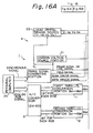
- FIGS. 16A through 18 are views showing a liquid crystal display unit according to a second embodiment of the present invention, in which Figs. 16A and 16B are a block diagram showing a general arrangement of the embodiment.
- the voltage applying part 4 comprises a liquid crystal driving power source 22 and a common voltage source portion 21.
- Numeral 23 denotes a three-state inverter, which inverts display data for every frame or line.
- Figures 17A to 17D explain a principle of assigning multiple gray-scale levels whose number is greater than the maximum number of gray-scale levels achievable by a data driver employed.
- a data driver for STN type liquid crystal that is able to simultaneously provide two voltage levels is employed to display 64 colors with 4 gray-scale levels.
- an image of one frame is once written in first and second field frame memories 13 and 14, and read therefrom at a speed of two times the write speed (double speed scanning) as shown in Fig. 6, to divide one frame into first and second fields.
- an gray-scale level 1 for example, is realized by applying 1.5 (V) to the first field and 2.5 (V) to the second field, to produce a mean effective voltage of 2 (V) for the one frame. This mean effective voltage is shown by hatching in Figs. 17A to 17D.
- An gray-scale level 2 is realized by applying 1.5 (V) to the first field and 4.5 (V) to the second field, to produce a mean effective voltage of 3 (V) for the one frame.
- An gray-scale level 3 is realized by applying 5.5 (V) to the first field and 2.5 (V) to the second field, to produce a mean effective voltage of 4 (V) for the one frame.
- An gray-scale level 4 is realized by applying 5.5 (V) to the first field and 4.5 (V) to the second field, to produce a mean effective voltage of 5 (V) for the one frame.
- the voltage levels for realizing the gray-scale level 1 in a positive frame are equal to those for realizing the gray-scale level 4 in a negative frame.
- the voltage levels for realizing the gray-scale level 1 in a negative frame are equal to those for realizing the gray-scale level 4 in a positive frame.
- the voltage levels for realizing the gray-scale level 2 in a positive frame are equal to those for realizing the gray-scale level 3 in a negative frame.
- the voltage levels for realizing the gray-scale level 2 in a negative frame are equal to those for realizing the gray-scale level 3 in a positive frame.
- common voltage level is inverted by the common voltage source portion 21 and display data is inverted by the three-state inverter 23 for every frame or line to utilize a small number of the voltage levels for applying different voltage levels to the first and second fields of each frame, respectively.
- gray-scale levels are assigned according to differences in the mean effective voltages in respective frames.
- Figure 18 shows an example of a driving waveform in each field according to this embodiment.
- An OFF voltage of a gate pulse of the three-state inverter 23 is -10 (V), and an ON voltage thereof 15 (V).
- the voltage applying part 4 in the liquid crystal display unit of this embodiment is simpler than that of the liquid crystal display unit in the first embodiment.
- FIGS. 20A through 27 are views showing a liquid crystal display unit according to a third embodiment of the present invention, in which Figs. 20A and 20B are a block diagram showing a general arrangement of the embodiment.
- Figs. 20A and 20B the same reference numerals as those shown in the first embodiment of Figs, 1A and 1B represent the same parts.
- a pixel selecting part 2 having a scan driver 7 and a data driver 8; a data signal generating part 3 having an A/D conversion portion 9, a data conversion portion 10, a first field frame memory 13, a second-field frame memory 14, and a display data switching portion 15; a voltage applying part 4 having a first frame liquid crystal driving source 16, a second frame liquid crystal driving source 17, and a switching circuit 18; a liquid crystal display part 5 having a liquid crystal display panel 19; and a timing signal generating portion 6 in Figs. 20A and 20B, but a common voltage source portion is omitted.
- a data conversion portion 10 of this embodiment uses, for example, a conversion table stored in a ROM (Read Only Memory) to swap predetermined gray-scale levels with one another according to digital input display data corresponding to gray-scale levels.
- ROM Read Only Memory
- Figures 21A and 21B show a result of measurement of characteristics of 64 gray-scale levels assigned with use of an eight-value digital driver (a digital data driver for eight gray-scale levels).
- Figure 22 shows a part of the eight-value digital driver 88 having a decoder circuit 881, eight analog switches 882, and eight data voltage lines 883 to which eight power source voltage V1 to V8 are applied.
- this eight-value digital driver 88 can realize eight gray-scale levels by switching ON one of the analog switches 882 in accordance with eight kinds of digital input signals. But when this eight-value digital driver 88 is installed in the circuit in Fig. 20, it can output 64 gray-scale levels.
- Figs. 21A and 21B shifts in the gray-scale levels are observed at positions over a gray-scale level 32. At these positions, the order of brightness is inverted.
- T-V Transmissivity-Voltage
- this embodiment rearranges the order of shifted gray-scale levels to provide normal gray-scale level characteristics.
- Figure 24 shows T-V characteristics of liquid crystal display panel 19 in Fig. 20 using the normal data signal.
- Fig. 24 it is clear that gray-scale levels 12 and 13 are shifted from normal positions. Accordingly, normal gray-scale levels are obtained by swapping input data for the gray-scale levels 12 and 13 with each other in this embodiment.
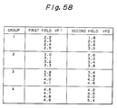
- Figure 27 shows an example of a driving waveform of this embodiment showing the field voltages of VF1 and VF2 to obtain gray-scale levels shown in Fig. 25.
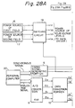
- Figures 28A and 29 are views showing a liquid crystal display unit according to a fourth embodiment of the present invention, in which Figs. 28A and 28B is a block diagram showing a general arrangement of this embodiment.
- Figs. 28A and 28B the same reference numerals as those shown in the third embodiment of Figs 20A and 28B denote the same parts.
- the liquid crystal display unit 1 of the third embodiment carries out the double speed scanning in displaying an image, while the liquid crystal display unit 1 of this embodiment does not carry out the same. Accordingly, the difference between the third embodiment and the fourth embodiment is that the display unit 1 of this embodiment is not provided with the first and second field frame memories 13 and 14 of the third embodiment of Fig. 20.
- a driving waveform shown in Fig. 29 of this embodiment is twice as long, along a temporal axis, as the driving waveform of Fig. 27, so that this embodiment is slightly disadvantageous in terms of flickering but requires no frame memories.
- Figures 30 through 39 are views showing a liquid crystal display unit according to a fifth embodiment of the present invention, in which Fig. 30 is a block diagram showing a general arrangement of the embodiment, In Fig. 30, the same reference numerals as those shown in the third embodiment of Fig. 20 represent the same parts.
- the liquid crystal display unit 1 of this embodiment has substantially the same arrangement as that of the third embodiment shown in Fig. 20 except that the data conversion portion 10 is not provided for this embodiment.
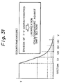
- this embodiment divides, as shown in Fig. 31, a range of applied voltage levels into a plurality (for example, four in this embodiment) of sections according to T-V characteristics of liquid crystal, and in each of the sect ions, carries out a field voltage selection.
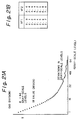
- Figure 33 shows a concrete example of a T-V characteristic curve of liquid crystal.
- 2(V) corresponds to a white level, i.e., a gray-scale level 0, and 5.15 (V) corresponds to a black level, i.e., a gray-scale level 63.
- Figure 34 shows gray-scale levels, digital input signals, and combinations of first and second field voltages VF1 and VF2 in assigning about 260,000 colors with 64 gray-scale levels with use of a 16-value data driver 8 and field voltage modulation with four divided sections.
- Figure 35 shows an example of a driving voltage waveform according to this embodiment.
- VF1 denotes a voltage of a first field in a positive frame
- VF2 denotes a voltage of a second field in the positive frame
- -VF1 denotes a voltage of a first field in a negative frame
- -VF2 denotes a voltage of a second field in the negative frame.
- Each voltage VF1, VF2, -VF1, and -VF2 involves data voltages shows as follows: +VF1(2.0, 2.1, 2.2, 2.3, 2.8, 2.9, 3.0, 3.1, 3.6, 3.7, 3.8, 3.9, 4.4, 4.5, 4.6, 4.7); +VF2(2.0, 2.4, 2.8, 3.2, 3.6, 4.0, 3.6, 4.0, 4.4, 4.8, 4.4, 4.8, 5.2, 5.6).
- -VF1 (-2.0, -2.1, -2.2, -2.3, -2.8, -2.9, -3.0, -3.1, -3.6, -3.7, -3.8, -3.9, -4.4, -4.5, -4.6, -4.7); -VF2(-2.0, -2.4, -2.8, -3.2, -3.6, -4.0, -3.6, -4.0, -4.4, -4.8, -4.4, -4.8, -5.2, -5.6).
- These voltages are switched from one to another and provided to the data driver 8.
- a voltage level corresponding to input data is selected and provided to drive a liquid crystal display panel 19.
- one frame corresponds to 16.7 ms, and a field period is 8.4 ms. With these conditions, the double speed scanning is carried out.
- Figures 36A and 36B through 39A and 39B are views showing driving waveforms in individual fields according to this embodiment.
- combinations of voltage levels and/or voltage level waveforms having different phases are applied to adjacent liquid crystal pixels, thereby reducing flickering due to fluctuations in transmissivity of a liquid crystal.
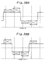
- Figs. 36A and 36B two sets of voltage levels are prepared and applied to each field, respectively, in Figs. 37A and 37B changing the combinations of the voltage levels of Figs. 36A and 36B is carried out, in Figs. 38A and 38B changing the phase of the voltage levels of Figs. 36A and 36B is carried out, and in Figs, 39A and 39B changing the combination and phase of the voltage levels of Figs. 36A and 36B is carried out.
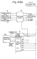
- Figures 40A and 41 are views showing a liquid crystal display unit according to a sixth embodiment of the present invention, in which Figs. 40A and 40B are a block diagram showing a general arrangement of the embodiment.
- Figs. 40A and 40B the same numerals as those of the fifth embodiment of Fig. 30 denote the same parts.
- the liquid crystal display unit 1 of the fifth embodiment carries out the double speed scanning, while the liquid crystal display unit 1 of this embodiment does not carry out the same so that the first and second field frame memories 13 and 14 of the fifth embodiment of Fig. 30 are not provided for this embodiment.
- a driving waveform of this embodiment shown in Fig. 41 is twice as long, along a temporal axis so that this embodiment is slightly disadvantageous in terms of flickering but advantageous in eliminating the frame memories.
- Figures 42A through 52 are views showing a liquid crystal display unit according to a seventh embodiment of the present invention, in which Figs. 42A and 42B is a block diagram showing the embodiment serving as a circuit for assigning 16 gray-scale levels with the use of an 8-gray-scale-level driver. Though this embodiment does not carry out double speed scanning, it can realize elimination of frame memories and suppression of flickering of 30 Hz.
- an A/D conversion portion 9 converts each of RGB data from a personal computer 20 into data of four bits (D0 to D3) corresponding to 16 gray-scale levels. Thereafter, a data conversion portion 10 converts the data into data of three bits (*D0 to *D2) for first and second fields, and according to the data of three bits, the data driver 8 selects eight-level power source voltages (*V1 to *V8) for assigning 16 gray-scale levels.
- Figure 43 is a table showing a relationship between input and output data of the data conversion portion 10
- Fig. 44 is a table showing a relationship between input data (gray-scale levels) of the data conversion portion 10, selected power source voltages, and mean output voltages. These relations may be expressed, for example, as a conversion table written in a ROM (not shown).
- input data for a gray-scale level 4 are [0011], and the first and second field voltages VF1 and VF2 are V2 and V3, respectively, so that a mean voltage will be (V2+V3)/2.
- input data for a gray-scale level 16 are all 1s, and the first and second field voltages VF1 and VF2 are V8 and V9, respectively, so that a mean voltage will be (V8+V9)/2.
- the gray-scale level 1 is the brightest level (a white level), and the gray-scale level 16 is the darkest level (a black level).
- a voltage difference between VF1 and VF2 is set to be smaller than a predetermined voltage (preferably 0.5 (V)) except for the gray-scale level 15 on the black level side. This is realized by setting the voltages V1 through V9 as, for example, 2.0 (V), 2.4 (V), 2.8, (V), 3.2 (V), 3.6 (V), 4.0 (V), 4.4 (V), 4.8 (V), and 5.2 (V). (Refer to Fig. 46.)
- the 30 Hz flickering is observed when different voltages are applied to fields, respectively, and when polarity is inverted in adjacent frames.
- the 30 Hz flickering may be solved by carrying out the double speed scanning with the use of frame memories to double the frequency of flickering to 60 Hz. This method, however, requires a memory to be provided for each frame, thereby increasing the cost and scale of a circuit.
- inventors of the present invention have considered a relationship between a voltage difference between fields and an optical response frequency, and repeatedly conducted tests. As a result, the inventors have found a range (a flickerless range) below a predetermined voltage difference where the flickering is not conspicuous.
- a hatched portion in Fig. 48 indicates the flickerless range.
- This range corresponds to a voltage difference of about 0.5 (V) or smaller between the first and second fields (or a difference of about 1 ⁇ 3 % or smaller in terms of flickering rate).
- V voltage difference
- Fig. 49A shows combinations of first field voltage VF1 and second field voltage VF2 applied to adjacent liquid crystal cells, respectively, and also, voltage polarities differ from each other between the cells.
- Figs. 49B to 49F show response waveforms of the adjacent liquid crystal cells shown in Fig. 49A. By applying the field voltage like this, different optical response waveforms may scatter over the surface uniformly, thereby more effectively suppressing the flickering between the cells.
- this embodiment inverts the polarities of voltages applied to adjacent cells, to differ the flickering phases of the adjacent cells by 180 degrees. This doubles a flickering frequency to 60 Hz in terms of surface average, thereby suppressing the 30 Hz flickering. In addition, a difference in field voltages in one frame is less than 0.5 (V) to surely suppress the 30 Hz flickering.
- a voltage difference of a gray-scale level 15 is 0.8 (V), which exceeds the preferable voltage difference (0.5 (V)). This causes no actual problem because the gray-scale level 15 is on the black level side where the flickering is inconspicuous.
- Voltage waveforms between adjacent cells are not limited to the above examples but may be as those shown in Figs. 50 through 52.
- Fig. 50 the combination and polarity of VF1 and VF2 are changed in a horizontal direction (data line direction: m, m+1), while the polarity of voltages is changed in a vertical direction (scan line direction: n,n+1).
- Fig. 51 the polarity of voltages is changed in the horizontal direction (data line direction: m, m+1), and combinations of VF1 and VF2 are changed in the vertical direction (scan line direction: n, n+1).
- Fig. 52 combinations of VF1 and VF2 are changed in the horizontal direction (data line direction: m, m+1), and the polarity of voltages is changed in the vertical direction (scan line direction: n, n+1).
- the flickering frequency may be doubled to 60 Hz in terms of surface average, thereby suppressing the 30 Hz flickering.
- Figures 53A to 58 are views showing a liquid crystal display unit according to an eighth embodiment of the present invention, in which Figs. 53A and 53B is a block diagram showing a general arrangement of the embodiment serving as a circuit for assigning 16 gray-scale levels with the use of an 8-gray-scale-level driver.
- V1m′ Vmin + (Vmax - Vmin) x 2m/(n - 1)
- V2m′ Vmin + (Vmax - Vmin) x 2mn 1 ⁇ 2 /(n - 1)
- Vmin is a minimum voltage in each section
- Vmax a maximum voltage in each section
- n the number of gray-scale levels in each section
- m being 0, 1, ...,n/2-1.
- Figure 54 shows voltages set according to the equations (1) and (2).
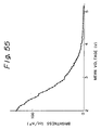
- Figures 55 and 56 show a relationship between a gray-scale level and brightness according to the above voltage sets.
- gray-scale levels are swapped with one another in a low brightness region, and in a high brightness region, a difference between gray-scale levels is narrowed although there is no swapping of gray-scale levels in the high brightness region.
- Figs. 57A and 57B which show a relationship between a change in brightness and a voltage difference
- the above phenomenon is conspicuous as the voltage difference becomes larger. If this happens, input image data may not be correctly regenerated.
- Fig. 23 shows causes of this sort of swapping of gray-scale levels and narrowed gray-scale levels.
- the brightness-voltage characteristics of a liquid crystal panel are not linear, and the brightness changes according to voltages in each field. If a difference between two voltages combined is too large, the brightness obtained will not be proportional to an average of the voltages but an average of brightness values obtained by the voltages respectively,so that the brightness obtained deviates from required brightness.
- the swapping of gray-scale levels or the narrowed gray-scale level differences may occur around a boundary where, on the one side of the boundary, a required brightness level is obtained according to a combination of the same voltages, and on the other side of the boundary, an obtained brightness level greatly deviates from a required brightness due to a combination of greatly differing voltages.
- numeral 30 denotes a write address counter, 31 a read address counter, 32 an address switching circuit, 33 a frame memory, INV1 and INV2 inverters, AND1 through AND4 AND gates, and NAND1 and NAND2 NAND gates.
- a first frame liquid crystal driving source 16 and a second frame liquid crystal driving source 17 generate, according to an idea of voltage setting of this embodiment, first field voltages VF1 (16 levels) and second field voltages VF2 (16 levels),respectively.
- a timing signal generating portion 6 sequentially doubles a vertical synchronous signal VSYNC to provide a signal 1/2 FCLK having a frequency which is twice the frame frequency.
- a driving source switching portion 18 is controlled according to the signal 1/2 FCLK, and switches the two sets of voltages according to fields, and provides the selected set to a data driver of 8 of the 16 gray-scale levels.
- An externally provided data signal of 6 bits for 64 gray-scale levels is written, according to a timing signal W/R for indicating write timing, in the frame memory at an address indicated by the write address counter 30, which receives a write address generating clock signal WCLK from the timing signal generating portion 6.
- the data are read two times in a period of one frame for one screen data according to a timing signal *W/R indicating read timing from a read address indicated by the read address counter 31, which receives a read address generating clock signal RCLK from the timing signal generating portion 6.
- bits b5 and b4 of the data for each of the first and second fields are provided as they are to the upper two bits D3 and D2 of the data driver of 8 of the 16 gray-scale levels.
- bits b3 and b2 for the first field and bits b1 and b0 for the second fields are swapped with one another through the data switching circuit, and provided to lower two bits D1 and D0 of the data driver of 8 of the 16 gray-scale levels.
- a scan driver 7 selects a scan line corresponding to the input data provided to the data driver 8 according to a clock signal SCLK having a frequency of about twice the frequency of a horizontal synchronous signal HSYN externally provided, thereby assigning, and cooperating with the data driver 8, a required gray-scale level.
- the same number of voltage levels are set for each of the two fields of one frame. Combinations of the voltage levels will form a maximum voltage Vmax and a minimum voltage Vmin with the number of combinations to be formed being n.
- V1m (Vmax + Vmin)/2 - (Vmax - Vmin)/(n 1 ⁇ 2 +1) + (Vmax - Vmin) x 2m/(n-1)
- V2m (Vmax + Vmin)/2-(Vmax - Vmin) x (n 1 ⁇ 2 /(n 1 ⁇ 2 +1) + (Vmax - Vmin) x 2mx 2 1 ⁇ 2 /(n-1)
- this embodiment sets voltages so as to minimize a difference in voltages to be switched from one to another.
- the embodiment therefore, is able to display an image with no swapping or narrowing of the gray-scale levels, and correctly assign multiple gray-scale levels with the use of an inexpensive data driver.
- gray-scale levels are assigned according to a mean effective voltage of voltage levels applied to fields of one frame, respectively, so that inexpensive drivers may be employed to assign multiple gray-scale levels.
- Figures 61 to 63B are views showing a liquid crystal display unit according to an ninth embodiment of the present invention, in which Fig. 61 is a block diagram showing a general arrangement of the embodiment serving as a circuit for assigning 64 gray-scale levels with the use of an 8-gray-scale-level driver 8.
- Fig. 61 the same numerals as those shown before represent the same parts, and only a power source 4, a timing signal generating portion 6, a scan driver 7, data drivers 8, a data conversion portion 10, a liquid crystal display panel 19, and personal computer 20 are shown.
- Figures 62A to 62D show driving waveforms for respective fields according to the ninth embodiment.
- the difference between the first embodiment to eighth embodiment and this embodiment is the driving waveforms to get gray-scale levels.
- a polarity of the applied field voltages are the same in one frame, but the polarity of the applied field voltage in this embodiment is altered in every field as shown in Figs. 62A to 62D.
- Fig. 63A according to this embodiment, combinations of first field voltage and second field voltage are applied to adjacent liquid crystal cells, respectively, and also, voltage polarities are different from each other between the cells.
- the field voltage like this, different optical response waveforms may scatter over the surface uniformly, thereby more effectively suppressing the flickering between the cells.
- asymmetrical field voltages are applied to the liquid crystal as shown in Fig. 63A, thereby generating the residual image on the liquid crystal panel as time goes by.
Description
- The present invention relates to liquid crystal display driver circuitry for use, for example, in controlling the data voltages of an active matrix liquid crystal display unit used in flat display panels, thereby to provide digital multiple gray-scale levels.
- In recent years, information terminals such as personal computers and word processors have become small in size, high in performance, and capable of many functions, and many compact information processors of desktop type, laptop type, and even smaller notebook type and palmtop type are now marketed.
- To reduce the size and weight of these information terminals, light-weight and thin display units are required. For this purpose, liquid crystal display units are frequently employed in place of cathode ray tubes (CRTs), which are usually employed for desktop information terminals. The liquid crystal display units include simple matrix liquid crystal display units such as TN (Twisted Nematic) display units and STN (Super Twisted Nematic) display units. Compared with these simple matrix display units, active matrix liquid crystal display units such as TFT (Thin Film Transistor) and MIM (Metal Insulator Metal) display units are frequently used for displaying high quality color images with multiple gray-scale levels, because the active matrix display units are capable of precisely controlling intermediate gray-scale levels, ensuring high contrast ratios, and providing a high response speed, compared with the simple matrix display units.
- For the active matrix liquid crystal display units, presently available digital driver ICs for selecting voltage levels for assigning gray-scale levels can handle only eight gray-scale levels. Even driver ICs presently being developed can operate only up to 16 gray-scale levels. To provide higher numbers of gray-scale levels, (i.e. more than 16), it has heretofore been necessary to employ expensive analog drivers to drive data, making it difficult to reduce the cost of liquid crystal display units.
- Various proposals have been made to increase the number of gray-scale levels with proper use of digital driver ICs. In one such proposal, a driver having a capacity of eight gray-scale levels is employed, and firstly, groups each involving one or more of the eight power source voltages are prepared and temporary switched from one to another and combined together, to realize a number of gray-scale levels greater than the number of the power sources.
- In this case, if a difference between voltages that are combined together is extremely large, transmissivity (based on an average of the combined voltages) may deviate from a required value, or a gray-scale level may be swapped with another one, resulting in deterioration of the quality of the gray-scale level definition.
- It is desirable, therefore, to provide an inexpensive digital data driver that can correctly provide multiple gray-scale levels.
- Conventional active matrix liquid crystal display units that achieve good display quality include those employing TFTs.
- The TFT display units employ many thin film transistors and pixel capacitance between two electrode layers to form a liquid crystal panel, and a display voltage is written in a selected capacitance through a corresponding thin film transistor.
- Brightness of the pixel depends on the written voltage. For example, "n" write voltages may be made available to provide "n" gray-scale levels.
- The n write voltages may be generated as follows:
- (1) A predetermined constant voltage is amplified through an operational amplifier whose amplification factor is variable in multiple steps (in this case, n steps). (This will be referred to as the first generation method.)
- (2) Two constant voltages are divided by resistances into n voltages, one of which is selected by a switching element. (This will be referred to as the second generation method.)
- Since the first generation method amplifies the predetermined constant voltage through the operational amplifier, it has the problem that a minimum variable width of the amplification factor is determined by the accuracy of the operational amplifier.
- Since the second generation method selects one of the two constant voltages through the switching element, it has the problem that the number of the voltage dividing resistances and switching elements must be increased to expand a circuit scale.
- Thus, neither one of the above methods can easily increase the number (n) of generated voltages, and therefore, those methods cannot further increase the number of gray-scale levels.
- According to a development in GUI (Graphic User Interface) in recent years, requirements for multiple colors in computer displays have escalated from conventional eight or 16 colors to 4096 colors with 16 gray-scale levels, or over 260,000 colors with 64 gray-scale levels. At present, however, about 512 colors with 8 gray-scale levels is the maximum, for the reasons mentioned above. This is completely insufficient to meet the above requirements for multiple colors.
- A method of increasing the number of gray scale brightness levels in such a liquid crystal display device is disclosed in US patent no. 4,921,334. This document discloses the use of an extra bit in the command for the gray scale voltage. When the extra bit is 0 then the brightness level is held the same over two successive frames. When the same bit is 1 then the voltage level is incremented between the frames and the eye sees the whiteness level as the average value of the two frames. Thus the number of gray scale levels may be doubled. This, however, is not sufficient to meet the above specifications.
- UK Patent no. 2,164,190 also discloses an attempt to increase the number of available gray scale brightness levels without significantly increasing the complexity of the drive circuitry. This device is very similar to that of the above mentioned US application and a single control bit is used to modify the data control signal between two successive frames. Once again the number of gray scale brightness levels can be doubled but no more and this is insufficient for the above mentioned specifications.
- It is desirable to provide an apparatus for controlling the data voltage of a liquid crystal display unit that can realize a high quality multiple gray-scale level display without significantly increasing circuit scale.
- In accordance with the invention there is thus provided an apparatus for controlling the data voltage of a liquid crystal display unit having a liquid crystal display panel, a scan driver, and a data bus driver to display successive single frame images, the apparatus comprising: a timing signal generating portion for generating at least timing signals for the scan driver and the data bus driver, and a timing signal for switching between fields; and the data bus driver selectively applying a data voltage from among voltage levels output thereto to the liquid crystal display panel, thereby assigning a gray-scale level according to a mean effective voltage of the voltage levels applied to each of the field of the successive single frames, characterised by a data signal generating part for dividing said single frame image into a plurality of fields and outputting the same to the data driver, and a voltage applying part for generating voltage levels for each of the fields independently of each other and outputting the same to the data driver.
- In this way, an embodiment of the present invention provides a gray-scale level according to a mean effective voltage of voltage levels applied to successive fields of a frame. This technique can provide multiple gray-scale levels without significantly increasing circuit scale.
- An embodiment of the invention changes the combination and/or phase of voltage levels applied to adjacent pixels, to suppress flickering. A further embodiment can increase a scan frequency according to the number of fields in a frame, to further suppress flickering.
- In addition, an embodiment of the invention can restrict a voltage difference applied to each frame below a predetermined value, to reduce flickering between a plurality of cells.
- An embodiment of the invention can substantially equalise averages of combinations of voltage levels set for a plurality of fields, thereby suppressing differences in the combined voltages, and securing the quality of a gray-scale level assignment.
- Reference will now be made, by way of example, to the accompanying drawings, in which:
- Fig. 1 is a block diagram showing part of a display device including circuitry according to a first embodiment of the present invention;
- Fig. 2 is a schematic circuit diagram showing a detailed construction of a liquid crystal panel shown in Fig. 1;
- Fig. 3 is a block diagram showing a detailed construction of a first field frame memory shown in Fig. 1;
- Figs. 4A and 4B are timing diagrams illustrating operation of the first field frame memory of Fig. 3;
- Fig. 5 is a view showing transmissivity-voltage (T-V) characteristics of liquid crystal;
- Fig. 6 is a schematic timing diagram illustrating double speed scanning of first and second field frame memories shown in Fig. 1;
- Figs. 7A to 7D are diagrams showing driving waveforms of a liquid crystal cell in the first embodiment;
- Figs. 8A and 8B are diagrams showing examples of driving waveforms in the first embodiment;
- Figs. 9A and 9B are diagrams corresponding to Figs. 8A and 8B but in which the combination of the voltage levels is changed from that of Figs. 8A and 8B;
- Figs. 10A and 10B are diagrams corresponding to Figs. 8A and 8B but in which the phases of the voltagel levels are changed from those of Figs. 8A and 8B;
- Figs. 11A and 11B are diagrams corresponding to Figs. 8A and 8B but in which the combination and phase of the voltage levels are changed from those of Figs. 8A and 8B;
- Figs. 12A to 12F are explanatory views relating to Figs. 8A and 8B;
- Figs. 13A to 13F are explanatory views relating to Figs. 9A and 9B;
- Figs. 14A to 14F are explanatory views relating to Fig:. 10A and 10B;
- Figs. 15A to 15F are explanatory views relating to Figs. 11A and 11B;
- Fig. 16 is a block diagram showing a display device including circuitry according to a second embodiment of the present invention;
- Figs. 17A to 17D are views showing driving waveforms of a liquid crystal cell in the second embodiment;
- Fig. 18 is a diagram showing an example of a driving waveform in the second embodiment;
- Fig. 19 is a diagram showing a comparative example of a driving waveform in the second embodiment;
- Fig. 20 is a block diagram showing a display device including circuitry according to a third embodiment of the present invention;
- Fig. 21A is a graph and Fig. 21B is a table illustrating characteristics of an assignment of 64 gray-scale levels;
- Fig. 22 is a block circuit diagram showing a digital data driver capable of providing eight gray-scale levels;
- Fig. 23 is a graph showing a T-V characteristic for illustrating causes of deviations in gray-scale levels;
- Fig. 24 is a graph illustrating a brightness/gray-scale level characteristic for explaining swapping of deviated gray-scale levels;
- Fig. 25 is table corresponding to Fig. 24;
- Fig. 26 is a table showing a conversion table of display data;
- Fig. 27 is a diagram illustrating examples of driving waveforms in the third embodiment;
- Fig. 28 is a block diagram showing a display device including circuitry according to a fourth embodiment of the present invention;
- Fig. 29 is a diagram showing examples of driving waveforms in the fourth embodiment;
- Figs. 30 is a block diagram showing a display device including circuitry according to a fifth embodiment of the present invention;
- Fig. 31 is a graph showing T-V characteristics for explaining a division of data voltage range;
- Fig. 32A is a graph and Fig. 32B is a table for illustrating characteristics of assigning 64 gray-scale levels;
- Fig. 33 is a graph illustrating the transmissivity-voltage characteristics of liquid crystal;
- Fig. 34 is a table showing gray-scale levels and the combinations of digital inputs;
- Fig. 35 is a diagram showing an example of a driving waveform in the fifth embodiment;
- Figs. 36A to 39B are diagrams showing further examples of driving waveforms in the fifth embodiment;
- Fig. 40 is a block diagram showing a display device including circuitry according to a sixth embodiment of the present invention;
- Fig. 41 is a diagram showing an example of a driving waveform in the sixth embodiment;
- Fig. 42 is a block diagram showing a display device including circuitry according to a seventh embodiment of the present invention;
- Fig. 43 is a table showing a conversion table of a data conversion circuit;
- Fig. 44 is a table showing a relationship between input data (a gray-scale level), selected power source voltages (for first and second fields), and a mean output voltage;
- Fig. 45 is a table showing combinations of voltages for 16 gray-scale levels, mean voltages, and voltage differences;
- Fig. 46 is a view showing examples of combinations of a first and second field voltages;
- Fig. 47 shows timing diagrams illustrating a flickering phenomena according to a field voltage modulation method (with no double scanning);
- Fig. 48 is an explanatory diagram showing a relationship between a voltage difference (VF1 - VF2) and flickering;
- Fig. 49A is a view showing examples of voltage waveforms between adjacent cells and Figs. 49B to 49F are timing diagrams illustrating response waveforms of the cells;
- Figs. 50 to 52 are diagrams showing further examples of voltage waveforms between adjacent cells;
- Fig. 53 is a block diagram showing a display device including circuitry according to an eighth embodiment of the present invention;
- Fig. 54 is a table showing set voltages calculated by previously-considered equations;
- Fig. 55 is a view showing a relationship between an average voltage and brightness according to a previously-considered voltage setting;
- Fig. 56 is a view showing the voltage setting of Fig. 55;
- Fig. 57A and 57B is a view explaining problems of the voltage setting of Fig. 55;
- Fig. 58 is a table showing set voltages calculated by equations pertaining to an embodiment of the present invention;
- Fig. 59 is a view showing a relationship between an average voltage and brightness according to a voltage setting of the embodiment;
- Fig. 60 is a view showing the voltage setting of the embodiment;
- Fig. 61 is a block diagram showing a display device including circuitry according to a ninth embodiment of the present invention;
- Fig. 62A to 62D are diagrams showing driving waveforms of liquid crystal cells in the ninth embodiment; and
- Figs. 63A and 63B are views showing examples of voltage waveforms between adjacent cells.
- Figures 1 through 15F are views showing a liquid crystal display unit according to a first embodiment of the present invention, in which Figs. 1A and 1B are a block diagram showing a general arrangement of the first embodiment. The arrangement of the first embodiment will be explained at first.
- In Figs. 1A and 1B, the liquid
crystal display unit 1 of the first embodiment basically comprises apixel selecting part 2, a datasignal generating part 3, avoltage applying part 4, a liquidcrystal display part 5, and a timingsignal generating portion 6. This embodiment is an example that realizes four gray-scale levels using a data driver for two gray-scale levels. Thepixel selecting part 2 involves ascan driver 7, anddata drivers 8. The data signal generatingpart 3 involves an A/D conversion portion 9, adata conversion portion 10, a firstparallel conversion portion 11, a secondparallel conversion portion 12, a first-field frame memory 13, a second-field frame memory 14, and a displaydata switching portion 15. Thevoltage applying part 4 involves a first-frame liquidcrystal driving source 16 serving as a voltage applying portion, a second-frame liquidcrystal driving source 17 serving as the voltage applying portion, a drivingsource switching portion 18, and a commonvoltage source portion 21. The liquidcrystal display part 5 involves a liquidcrystal display panel 19. - Figure 2 shows a detailed construction of the liquid
crystal display panel 19. The liquidcrystal display panel 19 involves 480 scan lines connected to thescan driver 7 respectively, 320 data lines for each of RGB elements connected to theupper data driver 8 and 320 data lines for each of RGB elements connected to thelower data driver 8. A thin film transistor (TFT) Q is provided close to every crossing point of each scan line and data line with its gate connected to the scan line, source connected to the data line, and drain connected to a liquid crystal element. And as shown by dotted line, three liquid crystal elements of R, G, and B form one pixel P. Accordingly, the liquidcrystal display panel 19 is a TFT active matrix liquid crystal display panel. -
Numeral 20 denotes a personal computer serving as an external device for providing data to be displayed on the liquidcrystal display unit 1. Thepersonal computer 20 provides the liquidcrystal display unit 1 with analog RGB signals and synchronous signals through an analog RGB interface. In this embodiment, thedata drivers 8 are for STN type liquid crystal, so that the digital data for each of R, G, and B requires only one bit. - The timing
signal generating portion 6 generates timing signals necessary for predetermined processes according to the synchronous signals, i.e., horizontal and vertical synchronous signals provided by thepersonal computer 20. For example, timing signals generated by the timingsignal generating portion 6, a scan driver signal, a data driver signal, and a field signal. - The A/
D conversion portion 9 digitizes the analog RGB signals provided by thepersonal computer 20, i.e., quantizes colors R, G, and B each with two bits. The A/D conversion portion 9 divides the digitized signal into two and outputs them separately as one bit signal for each R, G, and B to thedata conversion portion 10. - The
data conversion portion 10 converts digital display data provided by the A/D conversion portion 9 depending on a driving method. - The first and second
parallel conversion portions data conversion portion 10 into a parallel 16-bit image signal. - The first and second
field frame memories field frame memory 13. The first field frame memory includes a three-state buffer 131 and a input/output (I/O)memory 132. The data from theparallel conversion portion 11 is written in the I/O memory 132 by the three-state buffer 131 when an output enable signal OE is at a high level and the written data is read out from the I/O memory 132 when the output enable signal OE is at a low level. At this write/read operation, reading speed of the data from thefirst frame memory 13 is twice as fast as the writing speed of the data to thefirst frame memory 13 in this embodiment. The reading speed of the data is twice as fast as the writing speed to reduce flickering. - Figures 4A includes timing charts explaining relations among a vertical synchronizing signal VSYNC, a horizontal synchronizing signal HSYNC, a double speed vertical synchronizing signal WVSYNC, and a double speed horizontal synchronizing signal WHSYNC under the condition that the static RAM is used as the frame memory. As shown in Fig. 4A, 525 horizontal synchronizing signals are included in one frame. Double speed scanning can be realized by transmitting two scan lines of image data to the data driver in one horizontal scanning period by using the frame memory. For example, the double speed scanning can be realized by writing an image data in the
horizontal synchronizing period 2H of the present frame to the frame memory and reading image data in thehorizontal synchronizing periods - Figures 4B includes timing charts showing one
horizontal synchronizing period 2H in Fig. 4A the time-scale of which is magnified. In Fig. 4B, HSYNC denotes a horizontal synchronizing signal, WADD denotes a write address, RADD denotes a read address, OE denotes an output enable signal, and WE denotes a write enable signal. Hereinafter, an explanation will be given as 200 groups of series-parallel converted image data (16 bit) are included in one horizontal scanning period. The frame memory becomes a write mode when the output enable signal OE is at a high level, and during this mode, data is written in the frame memory at the rise up of the write enable signal WE. Further, the frame memory becomes read mode when the output enable signal OE is at a low level, and during this mode, data is output in accordance with the address. At this operation, to avoid the collision of write data and read data, it is necessary to provide a three-state buffer in the data bus line. The output enable signal OE can be used as the control signal of the three-state buffer, so that the output of the three-state buffer has a high impedance when the output enable signal OE is at a low level. Furthermore, the output enable signal OE can also be used for switching the write address and the read address, and the write address is selected when the output enable signal OE is at a high level and the read address is selected when the output enable signal OE is low level. - Now in Fig. 4B, a first group of data signals in the
horizontal synchronizing period 2H is applied to the three-state buffer and the output enable signal OE is at a high level, so that data is written to the frame memory at the rise of the write enable signal WE. After that, when the output enable signal OE is at a low level, data according to the write address is output from the frame memory and it is taken into the data driver at the rise of the latch signal LATCH. The read address has set in order such that the first and the second groups of data signals in the preceedinghorizontal synchronizing period 4H are output at this time. In this way, an image data of one line can be read in a half time of one horizontal scanning period. Namely, the image data of one display panel (= the image data of one frame) can be displayed in a half time of one frame. - The display
data switching portion 15 switches display data stored in the first and secondfield frame memories data drivers 8. These data signals are used to select the data voltage applied to thedata drivers 8 and will be explained hereinafter. - Each of the first and second frame liquid
crystal driving sources crystal driving source 16 provides V1 = 14 (V), V2 = 10 (V), V3 = 6 (V), and V4 = 2 (V), while the second frame liquidcrystal driving source 17 provides V1 = 12 (V), V2 = 10 (V), V3 = 6 (V), and V4 = 4 (V). Though a common voltage level for above-described voltages is 8 (V), it is set to 7 (V) by the commonvoltage source portion 21 since a source potential changes by about -1 (V) due to parasitic capacitance. - The driving
source switching portion 18 switches the first and second frame liquidcrystal driving sources data drivers 8 from the first or second frame liquidcrystal driving sources data drivers 8 from the displaydata switching portion 15. In other words, the data signal works as a data voltage selecting signal in thedata drivers 8. - Figure 5 explains a principle of assigning multiple gray-scale levels whose number is greater than the maximum number of gray-scale levels achievable by an employed data driver. For example, a data driver for STN type liquid crystal that is able to simultaneously provide two voltage levels is employed to display 64 colors with 4 gray-scale levels.
- First, an image of one frame is written in the first and second
field frame memories scale level 1 shown in Figs. 7A to 7D, for example, is realized by applying a voltage of 2 (V) to each of the first and second fields to produce a mean effective voltage of 2 (V) for the one frame. This mean effective voltage is shown by hatching in Figs. 7A to 7D. A gray-scale level 2 is realized by applying 2 (V) to the first field and 4 (V) to the second field to produce a mean effective voltage of 3 (V) for the one frame. To realize an gray-scale level 3, 6 (V) is applied to the first field and 2 (V) to the second field to produce a mean effective voltage of 4 (V) for the one frame. To realize an gray-scale level 4, 6 (V) is applied to the first field and 4 (V) to the second fields to produce a mean effective voltage of 5 (V) for the one frame. - In this way, different voltage levels are applied to the first and second fields, respectively, and differences in mean effective voltages occurring in individual frames can realize more gray-scale levels than the gray-scale levels realized by applied data voltages. Namely, an intermediate gray-scale level between two gray-scale levels due to two applied voltages can be realized by the mean effective voltage only.
- Figures 8A and 8B through 11A and 11B show examples of driving waveforms for respective fields according to the embodiment. For the sake of easy understanding, Figs. 8A and 8B through 11A and 11B will be explained with reference to Figs. 12A to 12F through 15A to 15F indicating the vertical synchronization, the data voltages, flickering, and synchronized flickering respectively. The value of the data voltages in Figs 12B and 12D through 15B and 15D is the voltage difference between the data voltage and the common voltage of 8 (V) in Figs. 8A and 8B through 11A and 11B.
- For example, the data voltage V4 is 6 (V) in Figs. 8A and 8B through 11A and 11B, but 2 (V) in Figs 12B and 12D through 15B and 15D since the difference between the data voltage of 6 (V) and the common voltage of 8 (V) in Figs. 8A and 8B through 11A and 11B is 2 (V).
- In Figs. 8A and 8B, two sets of voltage levels are prepared and applied to the fields, respectively. For example, in Figs. 12B and 12D, which are corresponding to Figs. 8A and 8B, the gray-
scale level 2 as shown in Fig. 7B is realized by applying voltages V4 (=2(V)) and V3 (=2(V)) to the first field, and voltages V2 (=4(V)) and V1 (=4(V)) to the second field. In adjacent liquid crystal cells, white and black are repeatedly displayed with the same flickering phase. Namely, the frequency of the synthesized flickering becomes 60 Hz, which is equal to the flickering frequency of each liquid crystal cell. - Figures 9A and 9B show examples of driving waveforms which are obtained by changing the combination of the voltage levels of Figs. 8A and 8B. As shown in Figs. 13B and 13D which are corresponding to Figs. 9A and 9B, the gray-
scale level 2 is realized by applying voltages V4 and V1 to the first field, and V2 and V3 to the second field. Also, voltages V3 and V2 are applied to a first field of another frame, and V1 and V4 to a second field thereof. White and black are repeatedly displayed in adjacent liquid crystal cells with flickering phases being different from each other by 180 degrees. - The frequency of synthesized flickering will be 120 Hz, so that the flickering becomes inconspicuous compared with that of Figs. 12B and 12D.
- Figures 10A and 10B show examples of driving waveforms obtainable by changing the phase of the voltage levels of Figs. 8A and 8B. As shown in Figs. 14B and 14D which are corresponding to Figs. 10A and 10B, the gray-
scale level 2 is realized by applying voltages V4 and V2 to the first field, and V2 and V3 to the second field. Also, voltages V3 and V1 are applied to a first field of another frame, and V1 and V4 to a second field thereof. Similar to Figs. 13B and 13D, white and black are repeatedly displayed in adjacent liquid crystal cells with the phases of flickering being different from each other by 180 degrees. Accordingly, the frequency of synthesized flickering will be 120 Hz. - This may make the flickering more inconspicuous compared with that of Figs. 12B and 12D.
- Figures 11A and 11B shows examples of driving waveforms which are obtainable by changing the combination and phase of the voltage levels of Figs. 8A and 8B. As shown in Figs. 15B and 15D which are corresponding to Figs. 11A and 11B, the gray-
scale level 2 is realized by applying voltages V4 and V4 to the first field, and V2 and V1 to the second field. Also, voltages V3 and V3 are applied to a first field of another frame, and V1 and V2 to a second field thereof. Similar to Figs. 12B and 12D, white and black are repeatedly displayed in adjacent liquid crystal cells with the same flickering phase. - The frequency of synthesized flickering will be 60 Hz, which is equal to the flickering frequency of each liquid crystal cell.
- Figures 16A through 18 are views showing a liquid crystal display unit according to a second embodiment of the present invention, in which Figs. 16A and 16B are a block diagram showing a general arrangement of the embodiment.
- In Figs. 16A and 16B, the same reference numerals as those of the first embodiment of Figs. 1A and 1B represent the same parts. In this embodiment, the
voltage applying part 4 comprises a liquid crystal drivingpower source 22 and a commonvoltage source portion 21.Numeral 23 denotes a three-state inverter, which inverts display data for every frame or line. - Figures 17A to 17D explain a principle of assigning multiple gray-scale levels whose number is greater than the maximum number of gray-scale levels achievable by a data driver employed. For example, a data driver for STN type liquid crystal that is able to simultaneously provide two voltage levels is employed to display 64 colors with 4 gray-scale levels.
- First, similar to the first embodiment, an image of one frame is once written in first and second
field frame memories scale level 1, for example, is realized by applying 1.5 (V) to the first field and 2.5 (V) to the second field, to produce a mean effective voltage of 2 (V) for the one frame. This mean effective voltage is shown by hatching in Figs. 17A to 17D. An gray-scale level 2 is realized by applying 1.5 (V) to the first field and 4.5 (V) to the second field, to produce a mean effective voltage of 3 (V) for the one frame. An gray-scale level 3 is realized by applying 5.5 (V) to the first field and 2.5 (V) to the second field, to produce a mean effective voltage of 4 (V) for the one frame. An gray-scale level 4 is realized by applying 5.5 (V) to the first field and 4.5 (V) to the second field, to produce a mean effective voltage of 5 (V) for the one frame. - Here, the voltage levels for realizing the gray-
scale level 1 in a positive frame are equal to those for realizing the gray-scale level 4 in a negative frame. Similarly, the voltage levels for realizing the gray-scale level 1 in a negative frame are equal to those for realizing the gray-scale level 4 in a positive frame. The voltage levels for realizing the gray-scale level 2 in a positive frame are equal to those for realizing the gray-scale level 3 in a negative frame. The voltage levels for realizing the gray-scale level 2 in a negative frame are equal to those for realizing the gray-scale level 3 in a positive frame. - Namely, only four kinds of voltage levels V1, V2, V3, and V4 are required in this embodiment to realize the same gray-scale levels in the first embodiment. In this embodiment, common voltage level is inverted by the common
voltage source portion 21 and display data is inverted by the three-state inverter 23 for every frame or line to utilize a small number of the voltage levels for applying different voltage levels to the first and second fields of each frame, respectively. As a result, gray-scale levels are assigned according to differences in the mean effective voltages in respective frames. - Figure 18 shows an example of a driving waveform in each field according to this embodiment. In Fig. 18, the liquid
crystal driving source 22 provide voltages of V1 = 6.5 (V), V2 = 3.5 (V), V3 = 2.5 (V), and V4 = 5.5 (V). Since a change (about -1 (V)) occurs in a source potential due to parasitic capacitance, the common voltage levels are set to 7 (V) and 0 (V). An OFF voltage of a gate pulse of the three-state inverter 23 is -10 (V), and an ON voltage thereof 15 (V). - Figure 19 shows a comparison example of a driving waveform in each field according to the first embodiment wherein the common voltage level is constant, As shown in Fig. 19, voltages of V1 = 13.5 (V), V2 = 10.5 (V), V3 = 9.5 (V), and V4 = 12.5 (V) are further required for the liquid
crystal driving source 22 other than the voltages required in Fig. 18. - Because of the inversion of the common voltage level, the
voltage applying part 4 in the liquid crystal display unit of this embodiment is simpler than that of the liquid crystal display unit in the first embodiment. - Figures 20A through 27 are views showing a liquid crystal display unit according to a third embodiment of the present invention, in which Figs. 20A and 20B are a block diagram showing a general arrangement of the embodiment. In Figs. 20A and 20B, the same reference numerals as those shown in the first embodiment of Figs, 1A and 1B represent the same parts. Accordingly, there are a
pixel selecting part 2 having ascan driver 7 and adata driver 8; a datasignal generating part 3 having an A/D conversion portion 9, adata conversion portion 10, a firstfield frame memory 13, a second-field frame memory 14, and a displaydata switching portion 15; avoltage applying part 4 having a first frame liquidcrystal driving source 16, a second frame liquidcrystal driving source 17, and aswitching circuit 18; a liquidcrystal display part 5 having a liquidcrystal display panel 19; and a timingsignal generating portion 6 in Figs. 20A and 20B, but a common voltage source portion is omitted. - A
data conversion portion 10 of this embodiment uses, for example, a conversion table stored in a ROM (Read Only Memory) to swap predetermined gray-scale levels with one another according to digital input display data corresponding to gray-scale levels. When multiple gray-scale levels are assigned with combinations of multiple voltage levels as achieved in the first and second embodiments, a problem occurs that gray-scale level characteristics shift. - Figures 21A and 21B show a result of measurement of characteristics of 64 gray-scale levels assigned with use of an eight-value digital driver ( a digital data driver for eight gray-scale levels). Figure 22 shows a part of the eight-value
digital driver 88 having adecoder circuit 881, eightanalog switches 882, and eightdata voltage lines 883 to which eight power source voltage V1 to V8 are applied. Normally, this eight-valuedigital driver 88 can realize eight gray-scale levels by switching ON one of the analog switches 882 in accordance with eight kinds of digital input signals. But when this eight-valuedigital driver 88 is installed in the circuit in Fig. 20, it canoutput 64 gray-scale levels. As shown in Figs. 21A and 21B, shifts in the gray-scale levels are observed at positions over a gray-scale level 32. At these positions, the order of brightness is inverted. - This is caused because, as shown in Fig. 23, T-V (Transmissivity-Voltage) characteristics of liquid crystal are nonlinear especially in the high field voltage part. Due to this nonlinearity, a transmissivity Ta which is an average of transmissivities T1 and T2 obtainable from field voltages VF1 and VF2 is different from a actual transmissivity Tv obtainable from an average voltage VFm = (VF1 + VF2) / 2.
- Accordingly, this embodiment rearranges the order of shifted gray-scale levels to provide normal gray-scale level characteristics. A principle of this will be explained with reference to Figs. 24 and 25, for the case of 4 values x 4 values = 16 gray-scale levels.
- Figure 24 shows T-V characteristics of liquid
crystal display panel 19 in Fig. 20 using the normal data signal. In Fig. 24, it is clear that gray-scale levels scale levels - Concretely, as shown in Fig. 26, input data [1011] for the gray-
scale level 12 and input data [1100] for the gray-scale level 13 are switched into [1100] for the gray-scale level 12 and [1011] for the gray-scale level 13. In this way, the gray-scale levels are swapped with each other to prevent the shift. - Figure 27 shows an example of a driving waveform of this embodiment showing the field voltages of VF1 and VF2 to obtain gray-scale levels shown in Fig. 25.
- Figures 28A and 29 are views showing a liquid crystal display unit according to a fourth embodiment of the present invention, in which Figs. 28A and 28B is a block diagram showing a general arrangement of this embodiment. In Figs. 28A and 28B, the same reference numerals as those shown in the third embodiment of Figs 20A and 28B denote the same parts.
- The liquid
crystal display unit 1 of the third embodiment carries out the double speed scanning in displaying an image, while the liquidcrystal display unit 1 of this embodiment does not carry out the same. Accordingly, the difference between the third embodiment and the fourth embodiment is that thedisplay unit 1 of this embodiment is not provided with the first and secondfield frame memories - As a result, a driving waveform shown in Fig. 29 of this embodiment is twice as long, along a temporal axis, as the driving waveform of Fig. 27, so that this embodiment is slightly disadvantageous in terms of flickering but requires no frame memories.
- Figures 30 through 39 are views showing a liquid crystal display unit according to a fifth embodiment of the present invention, in which Fig. 30 is a block diagram showing a general arrangement of the embodiment, In Fig. 30, the same reference numerals as those shown in the third embodiment of Fig. 20 represent the same parts.
- The liquid
crystal display unit 1 of this embodiment has substantially the same arrangement as that of the third embodiment shown in Fig. 20 except that thedata conversion portion 10 is not provided for this embodiment. - To deal with the problem that gray-scale level characteristics shift when multiple gray-scale levels are assigned with combinations of multi-valued voltage levels, this embodiment divides, as shown in Fig. 31, a range of applied voltage levels into a plurality (for example, four in this embodiment) of sections according to T-V characteristics of liquid crystal, and in each of the sect ions, carries out a field voltage selection.
- Namely, by dividing the range of applied voltage levels into sections, non-linearity of the T-V characteristics is relaxed and linearly corrected in each of the sections, thereby correcting a deviation between an actual transmissivity and a transmissivity obtained from a mean voltage, and realizing normal gray-scale level characteristics.
- Figures 32A and 32B shows a result of a measurement of gray-scale level characteristics over a whole range of applied voltage levels divided into four sections each involving four voltage levels to assign 4 values x 4 values = 16 gray-scale levels.
- Figure 33 shows a concrete example of a T-V characteristic curve of liquid crystal. In this case, 2(V) corresponds to a white level, i.e., a gray-
scale level 0, and 5.15 (V) corresponds to a black level, i.e., a gray-scale level 63. - Figure 34 shows gray-scale levels, digital input signals, and combinations of first and second field voltages VF1 and VF2 in assigning about 260,000 colors with 64 gray-scale levels with use of a 16-
value data driver 8 and field voltage modulation with four divided sections. - Figure 35 shows an example of a driving voltage waveform according to this embodiment. In the figure, VF1 denotes a voltage of a first field in a positive frame, VF2 denotes a voltage of a second field in the positive frame, -VF1 denotes a voltage of a first field in a negative frame, and -VF2 denotes a voltage of a second field in the negative frame. Each voltage VF1, VF2, -VF1, and -VF2 involves data voltages shows as follows:
+VF1(2.0, 2.1, 2.2, 2.3, 2.8, 2.9, 3.0, 3.1, 3.6, 3.7, 3.8, 3.9, 4.4, 4.5, 4.6, 4.7);
+VF2(2.0, 2.4, 2.8, 3.2, 3.6, 4.0, 3.6, 4.0, 4.4, 4.8, 4.4, 4.8, 5.2, 5.6).
-VF1(-2.0, -2.1, -2.2, -2.3, -2.8, -2.9, -3.0, -3.1, -3.6, -3.7, -3.8, -3.9, -4.4, -4.5, -4.6, -4.7);
-VF2(-2.0, -2.4, -2.8, -3.2, -3.6, -4.0, -3.6, -4.0, -4.4, -4.8, -4.4, -4.8, -5.2, -5.6). - These voltages are switched from one to another and provided to the
data driver 8. Among voltages provided by thedata driver 8, a voltage level corresponding to input data is selected and provided to drive a liquidcrystal display panel 19. Here, one frame corresponds to 16.7 ms, and a field period is 8.4 ms. With these conditions, the double speed scanning is carried out. - Figures 36A and 36B through 39A and 39B are views showing driving waveforms in individual fields according to this embodiment. As explained with reference to Figs. 8A and 8B through 11A and 11B, combinations of voltage levels and/or voltage level waveforms having different phases are applied to adjacent liquid crystal pixels, thereby reducing flickering due to fluctuations in transmissivity of a liquid crystal.
- In Figs. 36A and 36B, two sets of voltage levels are prepared and applied to each field, respectively, in Figs. 37A and 37B changing the combinations of the voltage levels of Figs. 36A and 36B is carried out, in Figs. 38A and 38B changing the phase of the voltage levels of Figs. 36A and 36B is carried out, and in Figs, 39A and 39B changing the combination and phase of the voltage levels of Figs. 36A and 36B is carried out.
- Figures 40A and 41 are views showing a liquid crystal display unit according to a sixth embodiment of the present invention, in which Figs. 40A and 40B are a block diagram showing a general arrangement of the embodiment. In Figs. 40A and 40B, the same numerals as those of the fifth embodiment of Fig. 30 denote the same parts.
- The liquid
crystal display unit 1 of the fifth embodiment carries out the double speed scanning, while the liquidcrystal display unit 1 of this embodiment does not carry out the same so that the first and secondfield frame memories - Compared with the driving waveform shown in Fig. 35, a driving waveform of this embodiment shown in Fig. 41 is twice as long, along a temporal axis so that this embodiment is slightly disadvantageous in terms of flickering but advantageous in eliminating the frame memories.
- Figures 42A through 52 are views showing a liquid crystal display unit according to a seventh embodiment of the present invention, in which Figs. 42A and 42B is a block diagram showing the embodiment serving as a circuit for assigning 16 gray-scale levels with the use of an 8-gray-scale-level driver. Though this embodiment does not carry out double speed scanning, it can realize elimination of frame memories and suppression of flickering of 30 Hz.
- In Figs. 42A and 42B, an A/
D conversion portion 9 converts each of RGB data from apersonal computer 20 into data of four bits (D0 to D3) corresponding to 16 gray-scale levels. Thereafter, adata conversion portion 10 converts the data into data of three bits (*D0 to *D2) for first and second fields, and according to the data of three bits, thedata driver 8 selects eight-level power source voltages (*V1 to *V8) for assigning 16 gray-scale levels. - Figure 43 is a table showing a relationship between input and output data of the
data conversion portion 10 and Fig. 44 is a table showing a relationship between input data (gray-scale levels) of thedata conversion portion 10, selected power source voltages, and mean output voltages. These relations may be expressed, for example, as a conversion table written in a ROM (not shown). - In Fig. 44, for example, input data for a gray-
scale level 1 are all zeroes by which VF1 is selected for both a first field voltage VF1 and a second field voltage VF2 and a mean voltage will be (V1+V1)/2=V1. Further, input data for a gray-scale level 4 are [0011], and the first and second field voltages VF1 and VF2 are V2 and V3, respectively, so that a mean voltage will be (V2+V3)/2. Furthermore, input data for a gray-scale level 16 are all 1s, and the first and second field voltages VF1 and VF2 are V8 and V9, respectively, so that a mean voltage will be (V8+V9)/2. - Here, the gray-
scale level 1 is the brightest level (a white level), and the gray-scale level 16 is the darkest level (a black level). As shown in Fig. 45, a voltage difference between VF1 and VF2 is set to be smaller than a predetermined voltage (preferably 0.5 (V)) except for the gray-scale level 15 on the black level side. This is realized by setting the voltages V1 through V9 as, for example, 2.0 (V), 2.4 (V), 2.8, (V), 3.2 (V), 3.6 (V), 4.0 (V), 4.4 (V), 4.8 (V), and 5.2 (V). (Refer to Fig. 46.) - As shown in Figs. 47A and 47B, the 30 Hz flickering is observed when different voltages are applied to fields, respectively, and when polarity is inverted in adjacent frames. The 30 Hz flickering may be solved by carrying out the double speed scanning with the use of frame memories to double the frequency of flickering to 60 Hz. This method, however, requires a memory to be provided for each frame, thereby increasing the cost and scale of a circuit.
- To deal with this, inventors of the present invention have considered a relationship between a voltage difference between fields and an optical response frequency, and repeatedly conducted tests. As a result, the inventors have found a range (a flickerless range) below a predetermined voltage difference where the flickering is not conspicuous.
- A hatched portion in Fig. 48 indicates the flickerless range. This range corresponds to a voltage difference of about 0.5 (V) or smaller between the first and second fields (or a difference of about 1 ∼ 3 % or smaller in terms of flickering rate). This means that, if combinations of voltages to be applied for a plurality of fields are determined such that a voltage difference between the applied voltages is less than the predetermined voltage difference (namely, if a difference between VF1 and VF2 is set to be less than 0. 5 (V)) on at least the white level side, the 30 Hz flickering will be inconspicuous.
- Further, as shown in Fig. 49A, according to this embodiment, combinations of first field voltage VF1 and second field voltage VF2 are applied to adjacent liquid crystal cells, respectively, and also, voltage polarities differ from each other between the cells. Figs. 49B to 49F show response waveforms of the adjacent liquid crystal cells shown in Fig. 49A. By applying the field voltage like this, different optical response waveforms may scatter over the surface uniformly, thereby more effectively suppressing the flickering between the cells.
- In this way, this embodiment inverts the polarities of voltages applied to adjacent cells, to differ the flickering phases of the adjacent cells by 180 degrees. This doubles a flickering frequency to 60 Hz in terms of surface average, thereby suppressing the 30 Hz flickering. In addition, a difference in field voltages in one frame is less than 0.5 (V) to surely suppress the 30 Hz flickering.
- In this embodiment, a voltage difference of a gray-
scale level 15 is 0.8 (V), which exceeds the preferable voltage difference (0.5 (V)). This causes no actual problem because the gray-scale level 15 is on the black level side where the flickering is inconspicuous. - Voltage waveforms between adjacent cells are not limited to the above examples but may be as those shown in Figs. 50 through 52. In Fig. 50, the combination and polarity of VF1 and VF2 are changed in a horizontal direction (data line direction: m, m+1), while the polarity of voltages is changed in a vertical direction (scan line direction: n,n+1). In Fig. 51, the polarity of voltages is changed in the horizontal direction (data line direction: m, m+1), and combinations of VF1 and VF2 are changed in the vertical direction (scan line direction: n, n+1). In Fig. 52 combinations of VF1 and VF2 are changed in the horizontal direction (data line direction: m, m+1), and the polarity of voltages is changed in the vertical direction (scan line direction: n, n+1).
- In any of the examples, the flickering frequency may be doubled to 60 Hz in terms of surface average, thereby suppressing the 30 Hz flickering.
- Figures 53A to 58 are views showing a liquid crystal display unit according to an eighth embodiment of the present invention, in which Figs. 53A and 53B is a block diagram showing a general arrangement of the embodiment serving as a circuit for assigning 16 gray-scale levels with the use of an 8-gray-scale-level driver.
- To assign 64 gray-scale levels with a digital driver IC of 16 gray-scale levels in the previous embodiments, arrangement of voltages for changing transmissivities is divided into four sections as shown in Fig. 31, and 16 voltage levels are prepared for each of the first and second fields. The 16 voltage levels are separated into four groups corresponding to the four sections.
- At this time, to equally distance mean values of combined voltages each involving two voltage levels from one another, the following equations have previously been considered:


where Vmin is a minimum voltage in each section, Vmax a maximum voltage in each section, n the number of gray-scale levels in each section, and m being 0, 1, ...,n/2-1. Figure 54 shows voltages set according to the equations (1) and (2). Namely, for each field, the voltages are separated into the first group, second group, and so on in the descending order, and voltages in the same group for the two fields are combined with one another. Accordingly, combinations in each group form 4 x 4 = 16 voltages, and the four groups provide 64 voltages, i.e., 64 gray-scale levels in total. - Figures 55 and 56 show a relationship between a gray-scale level and brightness according to the above voltage sets. As is apparent in the figures, gray-scale levels are swapped with one another in a low brightness region, and in a high brightness region, a difference between gray-scale levels is narrowed although there is no swapping of gray-scale levels in the high brightness region.
- In Figs. 57A and 57B which show a relationship between a change in brightness and a voltage difference, the above phenomenon is conspicuous as the voltage difference becomes larger. If this happens, input image data may not be correctly regenerated. The previously explained Fig. 23 shows causes of this sort of swapping of gray-scale levels and narrowed gray-scale levels. The brightness-voltage characteristics of a liquid crystal panel are not linear, and the brightness changes according to voltages in each field. If a difference between two voltages combined is too large, the brightness obtained will not be proportional to an average of the voltages but an average of brightness values obtained by the voltages respectively,so that the brightness obtained deviates from required brightness.
- For example, the swapping of gray-scale levels or the narrowed gray-scale level differences may occur around a boundary where, on the one side of the boundary, a required brightness level is obtained according to a combination of the same voltages, and on the other side of the boundary, an obtained brightness level greatly deviates from a required brightness due to a combination of greatly differing voltages.
- This embodiment intends to suppress this sort of deterioration of display quality. In Figs. 53A and 53B, numeral 30 denotes a write address counter, 31 a read address counter, 32 an address switching circuit, 33 a frame memory, INV1 and INV2 inverters, AND1 through AND4 AND gates, and NAND1 and NAND2 NAND gates.
- With this arrangement, a first frame liquid
crystal driving source 16 and a second frame liquidcrystal driving source 17 generate, according to an idea of voltage setting of this embodiment, first field voltages VF1 (16 levels) and second field voltages VF2 (16 levels),respectively. A timingsignal generating portion 6 sequentially doubles a vertical synchronous signal VSYNC to provide asignal 1/2 FCLK having a frequency which is twice the frame frequency. A drivingsource switching portion 18 is controlled according to thesignal 1/2 FCLK, and switches the two sets of voltages according to fields, and provides the selected set to a data driver of 8 of the 16 gray-scale levels. - An externally provided data signal of 6 bits for 64 gray-scale levels is written, according to a timing signal W/R for indicating write timing, in the frame memory at an address indicated by the
write address counter 30, which receives a write address generating clock signal WCLK from the timingsignal generating portion 6. The data are read two times in a period of one frame for one screen data according to a timing signal *W/R indicating read timing from a read address indicated by the readaddress counter 31, which receives a read address generating clock signal RCLK from the timingsignal generating portion 6. - At this time, voltages must be selected so that a gray-scale level indicated by the data is realized with two fields. For this purpose, the upper two bits b5 and b4 of the data for each of the first and second fields are provided as they are to the upper two bits D3 and D2 of the data driver of 8 of the 16 gray-scale levels. On the other hand, among lower four bits of the data, bits b3 and b2 for the first field and bits b1 and b0 for the second fields are swapped with one another through the data switching circuit, and provided to lower two bits D1 and D0 of the data driver of 8 of the 16 gray-scale levels.
- A
scan driver 7 selects a scan line corresponding to the input data provided to thedata driver 8 according to a clock signal SCLK having a frequency of about twice the frequency of a horizontal synchronous signal HSYN externally provided, thereby assigning, and cooperating with thedata driver 8, a required gray-scale level. - In more detail, as shown in Fig. 58, the same number of voltage levels are set for each of the two fields of one frame. Combinations of the voltage levels will form a maximum voltage Vmax and a minimum voltage Vmin with the number of combinations to be formed being n. Voltages applied to the two fields are V1m and V2m (m being 0, 1,..., (n1/2-1)), respectively, and set as follows:


With this setting, an average voltage of each of the two voltage groups to be combined together becomes substantially identical. As a result, a voltage difference between the maximum and minimum voltages is minimized in each group, so that, as shown in Figs. 59 and 60, gray-scale levels will cause no swapping or narrowing, thereby improving the quality of an image displayed with multiple gray-scale levels. Bias voltages of -0.025 (V) and +0.025 (V) have been added to the values. - In this way, when employing the field voltage modulation method to assign gray-scale levels whose number exceeds the number of gray-scale levels controlled by a data driver, this embodiment sets voltages so as to minimize a difference in voltages to be switched from one to another. The embodiment, therefore, is able to display an image with no swapping or narrowing of the gray-scale levels, and correctly assign multiple gray-scale levels with the use of an inexpensive data driver.
- As mentioned above, according to the embodiments of the invention which carry out the double speed scanning, gray-scale levels are assigned according to a mean effective voltage of voltage levels applied to fields of one frame, respectively, so that inexpensive drivers may be employed to assign multiple gray-scale levels.
- As a result, a high quality multiple gray-scale level assignment is realized at a low cost.
- Although the above embodiments carry out the double speed scanning by increasing a scan frequency, this technique never limits the invention. Alternatively, combinations of voltages may be changed for every frame to drive liquid crystal cells.
- Figures 61 to 63B are views showing a liquid crystal display unit according to an ninth embodiment of the present invention, in which Fig. 61 is a block diagram showing a general arrangement of the embodiment serving as a circuit for assigning 64 gray-scale levels with the use of an 8-gray-scale-
level driver 8. In Fig. 61, the same numerals as those shown before represent the same parts, and only apower source 4, a timingsignal generating portion 6, ascan driver 7,data drivers 8, adata conversion portion 10, a liquidcrystal display panel 19, andpersonal computer 20 are shown. - Figures 62A to 62D show driving waveforms for respective fields according to the ninth embodiment. The difference between the first embodiment to eighth embodiment and this embodiment is the driving waveforms to get gray-scale levels. In the former embodiments, a polarity of the applied field voltages are the same in one frame, but the polarity of the applied field voltage in this embodiment is altered in every field as shown in Figs. 62A to 62D.
- Further, as shown in Fig. 63A, according to this embodiment, combinations of first field voltage and second field voltage are applied to adjacent liquid crystal cells, respectively, and also, voltage polarities are different from each other between the cells. By applying the field voltage like this, different optical response waveforms may scatter over the surface uniformly, thereby more effectively suppressing the flickering between the cells. However, when applying field voltages as shown in Fig. 63A, asymmetrical field voltages are applied to the liquid crystal as shown in Fig. 63A, thereby generating the residual image on the liquid crystal panel as time goes by.
- For preventing this residual image on the the liquid crystal panel, usually field voltages are applied as shown in Fig. 63B wherein the applied field voltage becomes totally symmetrical. In this way, in this embodiment the polarities of voltages applied to adjacent cells are inverted, to reduce flickering.
Claims (14)
- An apparatus for controlling the data voltage of a liquid crystal display unit having a liquid crystal display panel (19), a scan driver (7), and a data bus driver (8) to display successive single frame images, the apparatus comprising:
a timing signal generating portion (6) for generating at least timing signals for the scan driver (7) and the data bus driver (8), and a further timing signal; and
the data bus driver (8) selectively applying a data voltage from among voltage levels output thereto to the liquid crystal display panel (19), thereby assigning a gray-scale level according to a mean effective voltage of the voltage levels applied to the successive single frames,
characterised by a data signal generating part (3) for dividing said single frame image into a plurality of fields and outputting the same to the data bus driver (8), wherein said further timing signal allows switching between the said fields, and
a voltage applying part (4) for generating voltage levels for each of the fields independently of each other and outputting the same to the data bus driver (8). - An apparatus as set forth in claim 1, wherein each of the successive single frames is formed of a first field and a second field and two successive frames are respectively odd and even frames;
the voltage applying part (4) generates voltage levels for the first field and the second field independently of each other;
the voltage applied to the data bus driver (8) from the voltage applying part is switched from the first field voltage to the second field voltage and vice versa at each field by the timing signal for switching the field; and
a plurality of voltage levels which differ relative to a common level are provided such that voltage levels in an odd frame are equal to those in an even frame. - An apparatus as set forth in claim 1 or claim 2, wherein the data signal generating part (3) includes at least one frame memory (13, 14), and
a reading speed of the data signal from the frame memory (13, 14) is faster than the writing speed of the data signal to the frame memory (13, 14). - An apparatus as set forth in claim 2, wherein the voltage applying part generates a binary common voltage level, and a plurality of voltage levels are switched from one to another relative to the binary common voltage level such that an absolute voltage value in a positive frame is equal to that in a negative frame.
- An apparatus as set forth in any preceding claim, wherein the data signal generating part includes a data conversion table, whereby the voltage levels applied by the voltage applying part are converted into preset gray-scale levels with use of the conversion table in order not to generate deviations in the displayed gray-scale levels.
- An apparatus as set forth in claim 5, wherein the conversion table comprises a ROM.
- An apparatus as set forth in any preceding claim, wherein the voltage applying part (4) generates a plurality of data voltage levels for each of the voltage ranges which are set by dividing the transmissivity-voltage characteristics of the liquid crystal pixels without overlapping; and
the data signal generating part (3) generates the data voltage selecting signal so as to select data voltage levels from each voltage range. - An apparatus as set forth in claim 7, wherein the data signal generating part (3) generates the data voltage selecting signal from which the combination of the voltage levels is changed between adjacent pixels.
- An apparatus as set forth in claim 7 or claim 8, wherein the data signal generating part (3) generates the data voltage selecting signal from which the phase of the voltage levels is changed between adjacent pixels.
- An apparatus as set forth in claim 7, 8 or 9, wherein the data signal generating part (3) generates the data voltage selecting signal from which the polarity of the voltage levels is changed between adjacent pixels.
- An apparatus as set forth in any preceding claim, wherein the data signal generating part (3) generates the data voltage selecting signal from which a combination of the applied voltages is determined such that a difference between the voltages applied to the fields respectively is below a predetermined value at least on a white level side.
- An apparatus as set forth in any preceding claim, wherein the data signal generating part (3) generates the data voltage selecting signal in order that averages of groups of the voltage levels prepared for a plurality of the fields may substantially be equal to one another between the fields, hence the voltages applied to the liquid crystal pixels are set according to transmissivity-voltage characteristics of the liquid crystal pixels such that the transmissivity changes at substantially equal intervals.
- An apparatus as set forth in any preceding claim, wherein one frame is formed of two fields, and the same number of voltage levels V1m and V2m (m being 0, 1, ..., (n1/2-1)) are set for the fields, respectively, as follows:


- An apparatus as set forth in claim 1, wherein each successive frame is formed of a first field and a second field and wherein successive frames are respectively positive and negative frames;
the voltage applying part (4) generates a binary common voltage level, and a plurality of voltage levels that differ relative to the binary common voltage level; and the value of the binary common voltage level is switched from one field to another such that an absolute voltage value in a positive frame is equal to that in a negative frame.
Applications Claiming Priority (6)
| Application Number | Priority Date | Filing Date | Title |
|---|---|---|---|
| JP29483190 | 1990-10-31 | ||
| JP294831/90 | 1990-10-31 | ||
| JP1310391 | 1991-02-04 | ||
| JP13103/91 | 1991-02-04 | ||
| JP218979/91 | 1991-08-29 | ||
| JP3218979A JP2761128B2 (en) | 1990-10-31 | 1991-08-29 | Liquid crystal display |
Publications (3)
| Publication Number | Publication Date |
|---|---|
| EP0484159A2 EP0484159A2 (en) | 1992-05-06 |
| EP0484159A3 EP0484159A3 (en) | 1992-08-12 |
| EP0484159B1 true EP0484159B1 (en) | 1995-09-20 |
Family
ID=27280119
Family Applications (1)
| Application Number | Title | Priority Date | Filing Date |
|---|---|---|---|
| EP91310075A Expired - Lifetime EP0484159B1 (en) | 1990-10-31 | 1991-10-31 | Liquid crystal display driver circuitry |
Country Status (5)
| Country | Link |
|---|---|
| US (1) | US6222515B1 (en) |
| EP (1) | EP0484159B1 (en) |
| JP (1) | JP2761128B2 (en) |
| KR (1) | KR950002283B1 (en) |
| DE (1) | DE69113206T2 (en) |
Cited By (1)
| Publication number | Priority date | Publication date | Assignee | Title |
|---|---|---|---|---|
| US7773066B2 (en) | 1999-03-26 | 2010-08-10 | Semiconductor Energy Laboratory Co., Ltd. | Liquid crystal display device |
Families Citing this family (53)
| Publication number | Priority date | Publication date | Assignee | Title |
|---|---|---|---|---|
| KR960008104B1 (en) * | 1991-05-21 | 1996-06-19 | 샤프 가부시끼가이샤 | Display apparatus, a drive circuit for a display apparatus, and a method of driving a display apparatus |
| JP3349527B2 (en) * | 1991-10-01 | 2002-11-25 | 株式会社日立製作所 | Liquid crystal halftone display |
| JP2831518B2 (en) * | 1992-10-30 | 1998-12-02 | シャープ株式会社 | Display device drive circuit |
| JP2849010B2 (en) * | 1992-11-25 | 1999-01-20 | シャープ株式会社 | Display device drive circuit |
| KR0140041B1 (en) * | 1993-02-09 | 1998-06-15 | 쯔지 하루오 | Power generator driving circuit and gray level voltage generator for lcd |
| JPH06274133A (en) * | 1993-03-24 | 1994-09-30 | Sharp Corp | Driving circuit for display device, and display device |
| JPH06347758A (en) * | 1993-06-02 | 1994-12-22 | Nec Corp | Driving method for liquid crystal display device |
| JP3275991B2 (en) * | 1994-07-27 | 2002-04-22 | シャープ株式会社 | Active matrix display device and driving method thereof |
| JP3277106B2 (en) * | 1995-08-02 | 2002-04-22 | シャープ株式会社 | Display drive |
| JP4147594B2 (en) * | 1997-01-29 | 2008-09-10 | セイコーエプソン株式会社 | Active matrix substrate, liquid crystal display device, and electronic device |
| GB2325555A (en) * | 1997-05-20 | 1998-11-25 | Sharp Kk | Light modulating devices |
| US7403213B1 (en) * | 1997-06-04 | 2008-07-22 | Texas Instruments Incorporated | Boundary dispersion for artifact mitigation |
| US6037918A (en) * | 1998-03-30 | 2000-03-14 | Candescent Technologies, Inc. | Error compensator circuits used in color balancing with time multiplexed voltage signals for a flat panel display unit |
| US6169529B1 (en) * | 1998-03-30 | 2001-01-02 | Candescent Technologies Corporation | Circuit and method for controlling the color balance of a field emission display |
| JP4637315B2 (en) | 1999-02-24 | 2011-02-23 | 株式会社半導体エネルギー研究所 | Display device |
| US7193594B1 (en) | 1999-03-18 | 2007-03-20 | Semiconductor Energy Laboratory Co., Ltd. | Display device |
| US6952194B1 (en) | 1999-03-31 | 2005-10-04 | Semiconductor Energy Laboratory Co., Ltd. | Liquid crystal display device |
| TW567363B (en) * | 1999-05-14 | 2003-12-21 | Seiko Epson Corp | Method for driving electrooptical device, drive circuit, electrooptical device, and electronic device |
| US6563482B1 (en) | 1999-07-21 | 2003-05-13 | Semiconductor Energy Laboratory Co., Ltd. | Display device |
| JP4797129B2 (en) * | 2000-06-16 | 2011-10-19 | 株式会社 日立ディスプレイズ | Active matrix display device |
| US7385579B2 (en) * | 2000-09-29 | 2008-06-10 | Semiconductor Energy Laboratory Co., Ltd. | Liquid crystal display device and method of driving the same |
| JP2002236472A (en) * | 2001-02-08 | 2002-08-23 | Semiconductor Energy Lab Co Ltd | Liquid crystal display device and its driving method |
| US7227517B2 (en) * | 2001-08-23 | 2007-06-05 | Seiko Epson Corporation | Electronic device driving method, electronic device, semiconductor integrated circuit, and electronic apparatus |
| JP2003177709A (en) * | 2001-12-13 | 2003-06-27 | Seiko Epson Corp | Pixel circuit for light emitting element |
| AU2003269500A1 (en) * | 2002-10-21 | 2004-05-04 | Semiconductor Energy Laboratory Co., Ltd. | Display device and driving method thereof |
| KR100486282B1 (en) * | 2002-11-16 | 2005-04-29 | 삼성전자주식회사 | Super Twisted Nematic LCD driver and driving method thereof |
| GB0307034D0 (en) * | 2003-03-27 | 2003-04-30 | Koninkl Philips Electronics Nv | Active matrix displays and drive control methods |
| KR100542319B1 (en) * | 2003-03-31 | 2006-01-11 | 비오이 하이디스 테크놀로지 주식회사 | Liquid Crystal Display Device |
| GB0319963D0 (en) * | 2003-08-27 | 2003-09-24 | Koninkl Philips Electronics Nv | Display device |
| JP2005351920A (en) * | 2004-06-08 | 2005-12-22 | Semiconductor Energy Lab Co Ltd | Control circuit for display device and display device and electronic equipment containing the same and driving method for the same |
| KR100624311B1 (en) * | 2004-08-30 | 2006-09-19 | 삼성에스디아이 주식회사 | Method for controlling frame memory and display device using the same |
| WO2006035953A1 (en) | 2004-09-27 | 2006-04-06 | Semiconductor Energy Laboratory Co., Ltd. | Display device and electronic device using the same |
| KR100701089B1 (en) * | 2004-11-12 | 2007-03-29 | 비오이 하이디스 테크놀로지 주식회사 | Method of realizing gray level of LCD |
| KR20060086021A (en) * | 2005-01-25 | 2006-07-31 | 삼성전자주식회사 | Display device and driving apparatus method of display device |
| US7705821B2 (en) * | 2005-01-31 | 2010-04-27 | Semiconductor Energy Laboratory Co., Ltd. | Driving method using divided frame period |
| US8253678B2 (en) * | 2005-03-15 | 2012-08-28 | Sharp Kabushiki Kaisha | Drive unit and display device for setting a subframe period |
| US7956876B2 (en) * | 2005-03-15 | 2011-06-07 | Sharp Kabushiki Kaisha | Drive method of display device, drive unit of display device, program of the drive unit and storage medium thereof, and display device including the drive unit |
| JP4444334B2 (en) * | 2005-03-15 | 2010-03-31 | シャープ株式会社 | LIQUID CRYSTAL DISPLAY DEVICE DRIVING METHOD, LIQUID CRYSTAL DISPLAY DEVICE DRIVE DEVICE, ITS PROGRAM AND RECORDING MEDIUM, AND LIQUID CRYSTAL DISPLAY DEVICE |
| JP4629096B2 (en) * | 2005-03-18 | 2011-02-09 | シャープ株式会社 | Image display device, image display monitor, and television receiver |
| US20090122207A1 (en) * | 2005-03-18 | 2009-05-14 | Akihiko Inoue | Image Display Apparatus, Image Display Monitor, and Television Receiver |
| US20060279561A1 (en) * | 2005-04-19 | 2006-12-14 | Semiconductor Energy Laboratory Co., Ltd. | Display device |
| US8212755B2 (en) * | 2005-05-24 | 2012-07-03 | Sharp Kabushiki Kaisha | Liquid crystal display device and driving method of the same |
| WO2007060783A1 (en) * | 2005-11-25 | 2007-05-31 | Sharp Kabushiki Kaisha | Image display method, image display device, image display monitor, and television receiver |
| US7847793B2 (en) | 2005-12-08 | 2010-12-07 | Semiconductor Energy Laboratory Co., Ltd. | Control circuit of display device, and display device and electronic appliance incorporating the same |
| KR101293560B1 (en) * | 2007-01-23 | 2013-08-06 | 삼성디스플레이 주식회사 | Display device and driving method thereof |
| DE102007020684A1 (en) * | 2007-05-03 | 2008-11-13 | Vastview Technology Inc. | Display panel driving method for an LCD involves setting a charging voltage compensation for brightness uniformity to brightness distribution on the display panel after setting at least two voltage-controls during frame period of panel |
| WO2009098705A1 (en) * | 2008-02-07 | 2009-08-13 | Raman Research Institute | A method to display gray shades in rms responding matrix display |
| TW200943270A (en) * | 2008-04-03 | 2009-10-16 | Faraday Tech Corp | Method and related circuit for color depth enhancement of displays |
| JP5797557B2 (en) * | 2009-11-27 | 2015-10-21 | シャープ株式会社 | Liquid crystal display device, television receiver |
| JP5370214B2 (en) * | 2010-02-25 | 2013-12-18 | セイコーエプソン株式会社 | Video processing circuit, video processing method, liquid crystal display device, and electronic apparatus |
| JP5685065B2 (en) * | 2010-11-29 | 2015-03-18 | ラピスセミコンダクタ株式会社 | Display device, halftone processing circuit, and halftone processing method |
| KR20160081655A (en) * | 2014-12-31 | 2016-07-08 | 삼성디스플레이 주식회사 | Display device, method for driving display device and method for minimizing afterimage of display device |
| CN113628578B (en) * | 2021-10-13 | 2021-12-31 | 常州欣盛半导体技术股份有限公司 | Source driver |
Family Cites Families (14)
| Publication number | Priority date | Publication date | Assignee | Title |
|---|---|---|---|---|
| US4481511A (en) * | 1981-01-07 | 1984-11-06 | Hitachi, Ltd. | Matrix display device |
| JPS5823090A (en) * | 1981-08-03 | 1983-02-10 | 株式会社日立製作所 | Display |
| US4775891A (en) * | 1984-08-31 | 1988-10-04 | Casio Computer Co., Ltd. | Image display using liquid crystal display panel |
| US4776676A (en) * | 1986-08-25 | 1988-10-11 | Canon Kabushiki Kaisha | Ferroelectric liquid crystal optical modulation device providing gradation by voltage gradient on resistive electrode |
| JPH083956B2 (en) * | 1986-09-18 | 1996-01-17 | 日本テキサス・インスツルメンツ株式会社 | Semiconductor memory device |
| JPH07104662B2 (en) * | 1987-01-23 | 1995-11-13 | ホシデン株式会社 | Liquid crystal display |
| US5041821A (en) * | 1987-04-03 | 1991-08-20 | Canon Kabushiki Kaisha | Ferroelectric liquid crystal apparatus with temperature dependent DC offset voltage |
| JP2612863B2 (en) * | 1987-08-31 | 1997-05-21 | シャープ株式会社 | Driving method of display device |
| JP2852042B2 (en) * | 1987-10-05 | 1999-01-27 | 株式会社日立製作所 | Display device |
| DE3856474T2 (en) * | 1987-11-12 | 2001-11-08 | Canon Kk | Liquid crystal device |
| JP2680090B2 (en) * | 1987-12-29 | 1997-11-19 | シャープ株式会社 | Field discriminator |
| US4921334A (en) | 1988-07-18 | 1990-05-01 | General Electric Company | Matrix liquid crystal display with extended gray scale |
| JPH02157813A (en) * | 1988-12-12 | 1990-06-18 | Sharp Corp | Liquid crystal display panel |
| JPH0335219A (en) * | 1989-06-30 | 1991-02-15 | Sharp Corp | Display device |
-
1991
- 1991-08-29 JP JP3218979A patent/JP2761128B2/en not_active Expired - Lifetime
- 1991-10-31 US US07/786,251 patent/US6222515B1/en not_active Expired - Lifetime
- 1991-10-31 KR KR1019910019261A patent/KR950002283B1/en not_active IP Right Cessation
- 1991-10-31 EP EP91310075A patent/EP0484159B1/en not_active Expired - Lifetime
- 1991-10-31 DE DE69113206T patent/DE69113206T2/en not_active Expired - Lifetime
Cited By (4)
| Publication number | Priority date | Publication date | Assignee | Title |
|---|---|---|---|---|
| US7773066B2 (en) | 1999-03-26 | 2010-08-10 | Semiconductor Energy Laboratory Co., Ltd. | Liquid crystal display device |
| US8125429B2 (en) | 1999-03-26 | 2012-02-28 | Semiconductor Energy Laboratory Co., Ltd. | Liquid crystal display device |
| US8149198B2 (en) | 1999-03-26 | 2012-04-03 | Semiconductor Energy Laboratory Co., Ltd. | Liquid crystal display device |
| US9373292B2 (en) | 1999-03-26 | 2016-06-21 | Semiconductor Energy Laboratory Co., Ltd. | Liquid crystal display device |
Also Published As
| Publication number | Publication date |
|---|---|
| JP2761128B2 (en) | 1998-06-04 |
| US6222515B1 (en) | 2001-04-24 |
| KR950002283B1 (en) | 1995-03-16 |
| DE69113206D1 (en) | 1995-10-26 |
| DE69113206T2 (en) | 1996-02-15 |
| JPH0546125A (en) | 1993-02-26 |
| EP0484159A3 (en) | 1992-08-12 |
| EP0484159A2 (en) | 1992-05-06 |
Similar Documents
| Publication | Publication Date | Title |
|---|---|---|
| EP0484159B1 (en) | Liquid crystal display driver circuitry | |
| EP0391655B1 (en) | A drive device for driving a matrix-type LCD apparatus | |
| TW559752B (en) | Liquid crystal display device, drive circuit, drive method and electronic equipment | |
| KR100748840B1 (en) | Liquid crystal display unit and driving method therefor | |
| JP5373587B2 (en) | Liquid crystal display device and driving method thereof | |
| KR100520861B1 (en) | Gray scale display reference voltage generating circuit and liquid crystal display device using the same | |
| KR100593765B1 (en) | LCD and its driving method | |
| US7667680B2 (en) | Liquid crystal display and driving method thereof | |
| US5874933A (en) | Multi-gradation liquid crystal display apparatus with dual display definition modes | |
| JP3534086B2 (en) | Driving method of liquid crystal display device | |
| US20140078035A1 (en) | Electrophoretic display device and driving method thereof | |
| TWI397734B (en) | Liquid crystal display and driving method thereof | |
| EP0767449B1 (en) | Method and circuit for driving active matrix liquid crystal panel with control of the average driving voltage | |
| US6320562B1 (en) | Liquid crystal display device | |
| JP3349638B2 (en) | Method and circuit for driving display device | |
| US5801671A (en) | Liquid crystal driving device | |
| JP3724301B2 (en) | Electro-optical device driving method, driving circuit thereof, electro-optical device, and electronic apparatus | |
| JPH11352464A (en) | Liquid crystal display device and liquid crystal panel | |
| JPH1124637A (en) | Drive method for simple matrix liquid crystal display | |
| JP3633943B2 (en) | Liquid crystal display | |
| JP3823645B2 (en) | Electro-optical device driving method, driving circuit thereof, electro-optical device, and electronic apparatus | |
| KR0160063B1 (en) | Lcd device | |
| KR100604272B1 (en) | Liquid crystal display apparatus and method for driving the same | |
| KR20000001238A (en) | Method of driving tft liquid crystal element |
Legal Events
| Date | Code | Title | Description |
|---|---|---|---|
| PUAI | Public reference made under article 153(3) epc to a published international application that has entered the european phase |
Free format text: ORIGINAL CODE: 0009012 |
|
| AK | Designated contracting states |
Kind code of ref document: A2 Designated state(s): DE FR GB IT NL |
|
| PUAL | Search report despatched |
Free format text: ORIGINAL CODE: 0009013 |
|
| AK | Designated contracting states |
Kind code of ref document: A3 Designated state(s): DE FR GB IT NL |
|
| 17P | Request for examination filed |
Effective date: 19921029 |
|
| 17Q | First examination report despatched |
Effective date: 19931227 |
|
| GRAA | (expected) grant |
Free format text: ORIGINAL CODE: 0009210 |
|
| ITF | It: translation for a ep patent filed |
Owner name: INTERPATENT ST.TECN. BREV. |
|
| AK | Designated contracting states |
Kind code of ref document: B1 Designated state(s): DE FR GB IT NL |
|
| REF | Corresponds to: |
Ref document number: 69113206 Country of ref document: DE Date of ref document: 19951026 |
|
| ET | Fr: translation filed | ||
| PLBE | No opposition filed within time limit |
Free format text: ORIGINAL CODE: 0009261 |
|
| STAA | Information on the status of an ep patent application or granted ep patent |
Free format text: STATUS: NO OPPOSITION FILED WITHIN TIME LIMIT |
|
| 26N | No opposition filed | ||
| REG | Reference to a national code |
Ref country code: GB Ref legal event code: IF02 |
|
| REG | Reference to a national code |
Ref country code: GB Ref legal event code: 732E |
|
| NLS | Nl: assignments of ep-patents |
Owner name: SHARP KABUSHIKI KAISHA Effective date: 20050726 |
|
| REG | Reference to a national code |
Ref country code: FR Ref legal event code: TP |
|
| PGFP | Annual fee paid to national office [announced via postgrant information from national office to epo] |
Ref country code: FR Payment date: 20101020 Year of fee payment: 20 Ref country code: NL Payment date: 20101016 Year of fee payment: 20 |
|
| PGFP | Annual fee paid to national office [announced via postgrant information from national office to epo] |
Ref country code: DE Payment date: 20101027 Year of fee payment: 20 |
|
| PGFP | Annual fee paid to national office [announced via postgrant information from national office to epo] |
Ref country code: GB Payment date: 20101027 Year of fee payment: 20 Ref country code: IT Payment date: 20101022 Year of fee payment: 20 |
|
| REG | Reference to a national code |
Ref country code: DE Ref legal event code: R071 Ref document number: 69113206 Country of ref document: DE |
|
| REG | Reference to a national code |
Ref country code: DE Ref legal event code: R071 Ref document number: 69113206 Country of ref document: DE |
|
| REG | Reference to a national code |
Ref country code: NL Ref legal event code: V4 Effective date: 20111031 |
|
| REG | Reference to a national code |
Ref country code: GB Ref legal event code: PE20 Expiry date: 20111030 |
|
| PG25 | Lapsed in a contracting state [announced via postgrant information from national office to epo] |
Ref country code: NL Free format text: LAPSE BECAUSE OF EXPIRATION OF PROTECTION Effective date: 20111031 |
|
| PG25 | Lapsed in a contracting state [announced via postgrant information from national office to epo] |
Ref country code: GB Free format text: LAPSE BECAUSE OF EXPIRATION OF PROTECTION Effective date: 20111030 |
|
| PG25 | Lapsed in a contracting state [announced via postgrant information from national office to epo] |
Ref country code: DE Free format text: LAPSE BECAUSE OF EXPIRATION OF PROTECTION Effective date: 20111101 |