EP0487941A2 - Testable integrated circuit and associated circuitry - Google Patents
Testable integrated circuit and associated circuitry Download PDFInfo
- Publication number
- EP0487941A2 EP0487941A2 EP91118772A EP91118772A EP0487941A2 EP 0487941 A2 EP0487941 A2 EP 0487941A2 EP 91118772 A EP91118772 A EP 91118772A EP 91118772 A EP91118772 A EP 91118772A EP 0487941 A2 EP0487941 A2 EP 0487941A2
- Authority
- EP
- European Patent Office
- Prior art keywords
- input
- output
- test
- data
- stage
- Prior art date
- Legal status (The legal status is an assumption and is not a legal conclusion. Google has not performed a legal analysis and makes no representation as to the accuracy of the status listed.)
- Ceased
Links
Images


Classifications
-
- G—PHYSICS
- G01—MEASURING; TESTING
- G01R—MEASURING ELECTRIC VARIABLES; MEASURING MAGNETIC VARIABLES
- G01R31/00—Arrangements for testing electric properties; Arrangements for locating electric faults; Arrangements for electrical testing characterised by what is being tested not provided for elsewhere
- G01R31/28—Testing of electronic circuits, e.g. by signal tracer
- G01R31/317—Testing of digital circuits
- G01R31/3181—Functional testing
- G01R31/3185—Reconfiguring for testing, e.g. LSSD, partitioning
- G01R31/318533—Reconfiguring for testing, e.g. LSSD, partitioning using scanning techniques, e.g. LSSD, Boundary Scan, JTAG
- G01R31/318572—Input/Output interfaces
-
- G—PHYSICS
- G01—MEASURING; TESTING
- G01R—MEASURING ELECTRIC VARIABLES; MEASURING MAGNETIC VARIABLES
- G01R31/00—Arrangements for testing electric properties; Arrangements for locating electric faults; Arrangements for electrical testing characterised by what is being tested not provided for elsewhere
- G01R31/28—Testing of electronic circuits, e.g. by signal tracer
- G01R31/317—Testing of digital circuits
- G01R31/3181—Functional testing
- G01R31/3185—Reconfiguring for testing, e.g. LSSD, partitioning
- G01R31/318533—Reconfiguring for testing, e.g. LSSD, partitioning using scanning techniques, e.g. LSSD, Boundary Scan, JTAG
- G01R31/318541—Scan latches or cell details
Definitions
- the invention relates to circuit modules and integrated circuits for the so-called boundary scan test method.
- the integrated circuits at logic inputs and logic outputs have test stages (boundary scan cells) which are arranged between the connection points and the functional logic.
- the Boundary-Scan test method is published in the magazine "Elektronik” in a series of articles in booklets 12 (pages 52-57) / 13 (pages 102-108) / 14 (pages 96-103) / 15 (pages 69-74) and 17 (pages 62-68) 1989.
- FIG. 5 shows an assembly with two integrated circuits and the test procedure is described in the accompanying text. Above all, this test procedure can be used to check the connecting cables from the connector strip of the module to the connections of the integrated modules and between the integrated modules; the functions of the logical blocks can also be checked.
- the boundary scan method has the advantage that only a few additional connection points have to be provided for the integrated circuits and on the module.
- Book 14, page 97, Figure 2 shows the arrangement of the test levels (scope ⁇ boundary scan cell).
- the test cells can be controlled for test purposes. This control takes place via a control device designated JTAG-Control, which consists of a serial control signal TMS generates several parallel control signals.
- the object of the invention is therefore to provide integrated circuits and assemblies for the boundary scan test method, which enable testing at maximum speed and in which the additional circuit complexity is reduced to a minimum.
- No further circuit element is inserted in the connecting lines between input connection points and functional logic of an integrated circuit.
- the test stages are expediently switched on after the bond connection.
- Protective circuits or isolating amplifiers can be located before the input test stage.
- the output test stage can still be installed before an output amplifier and / or protective circuits.
- the memory stages of the output test stages are directly connected to a shift register without any further logic elements.
- the separate control of the multiplexers of the input test stages and the output test stages is particularly advantageous.
- a controller is then not required in the integrated circuit, since the information at the data outputs of the output test stages changes continuously in accordance with the test data signal TDI, by separating the control lines or the control signals for the input-side and output-side shift register chain, that is achieved
- only the data output by the function logic can be specified at the outputs of the output test stages and thus the connection points of the integrated module.
- a combination of the input test stages and output test stages used is used for bidirectional connections of the integrated modules. These also have a control section so that the direction of the data flow can also be controlled via a tri-state output stage. However, an additional connection point of the integrated circuit is required for this. In the case of a data bus, the associated output stages are controlled by a common control section.
- both control lines are also led out to the connector strip or a separate test connector strip of the module.
- One controller on the module can then be dispensed with.
- the previously required controller can also be used on the module, which then controls the test process for all integrated modules. This saves one connection point or two connection points in the assembly.
- the integrated module IC has a functional logic FL, in which the logical connections are established which are required to implement a desired function.
- the functional logic can be a combination of logic gates, it can also be a combination of memory stages with gates, pure memory stages or also microprocessors and so on.
- Input test stages (scan input cells) EPS1 to EPSn are connected between the input connection points (pins) EP1, EP2, ... EPn of the integrated module and inputs of the function logic.
- Output test stages (scan output cells) APS1 to APSf are likewise switched on between outputs of the functional logic FL and output connection points AP1 to APf.
- the stages of the memory stages EPS1 to APSf can be switched in a chain and then form a shift register.
- a test data signal TDI is fed to the first input test stage EPS1 via a test data input TDE.
- the test data can run through all test stages and, for example, can be output unchanged at the test data output TDA of the last output test stage APSf as the output test data signal TDO.
- the test data are clocked with a test clock signal TC.
- the input test stages and the output test stages can be controlled separately via control signals MS1 or MS2.
- An input test stage EPS is shown in detail in FIG.
- An input connection point (pin) EP is connected directly to the functional logic FL via a connecting line ESL.
- the first input A1 of an input multiplexer MUX1 is connected to this connecting line (after the bond line and, if appropriate, protective circuits and / or input buffers).
- Input data ED can be switched through to the multiplexer output via this input.
- the second multiplexer input B1 represents the data input DE1 for the test data signal TDI.
- the output of the multiplexer is connected to the data input of an input memory stage FF1, for example a D flip-flop. An output of this flip-flop represents the data output DA1.
- the input clock stage FF1 is also supplied with the test clock signal TC via a clock input TE.
- the data output DA1 of the first input test stage is connected to the data input DE1 (DE12) of the second test stage and so on, as can be seen in FIG. 4.
- the data inputs and data outputs are provided with a further number in accordance with the numbering of the input test stages.
- An output test stage APS is shown in FIG.
- the functional logic FL is connected to a first input A2 of an output multiplexer MUX2, the output of which is led to an output connection point (pin) AP.
- An output memory stage FF2 is connected upstream of a second input B2 of the output multiplexer MUX2, the data input of which is designated DE2 and the data output of which is designated DA2.
- the output memory stage is also clocked by the test clock signal TC.
- the output multiplexer MUX2 can be switched over by an output mode control signal MS2.
- an output amplifier (buffer) or a protective circuit can also be connected between the output of the output multiplexer and the connection point or the bond line.
- the data input DE2 of the first output test stage is connected to the data output DA1 (DA1n in FIG. 4) of the last input test stage EPSn.
- a data input DE2 of the following output test stage is connected to the data output DA2 of the previous output test stage, as can also be seen in FIG. 4.
- the data inputs and data outputs are each provided with a second digit in accordance with the numbering of the output test stages.
- the memory stages FF1 of the input test stages can take over the input information ED present at the input connection points EP in parallel.
- test data TDI can be entered via the input test stages into the memory stages FF2 of the output test stages via the test data input TDE. These always form an output shift register, the shifted information of which is always output serially at the test data output TDA.
- the output test information is designated TDO; it can coincide with the test data signal TDI being pushed through, but, as described above, can also be formed by the input data ED.
- connection points EP Via the input connection points EP, different input combinations can be applied to the integrated circuit and thus to the inputs of the functional logic FL, the function of which is checked on the basis of the output data AD output at the output connection points AP. If the output connection points are routed to the module's connector strip, a check can also be carried out here directly. If, on the other hand, the output connection points AP of the integrated module are routed to inputs of one or more integrated modules, the logic data present can in turn be tested via their input and output test circuits.
- the output test data TDO are continuously transferred from the output of the memory stage FF1 of the last input test stage to the output shift register (all memory stages FF2) and output.
- the output multiplexers MUX2 switch through the output data AD, they do not interfere. In this way the functional logic can be checked and test data can already be transferred to the output shift register.
- connection points AP are switched through to check the connected lines to the output connection points AP. If these are connected to connection points of the connector strip of the module, they can be checked directly, otherwise - as with the function logic check - they must first be read into the input memory stages FF1 via the input test stage of the connected modules and after the test data signal TDO has been output be rated. If a 0101 sequence, 0011 sequence, etc. is selected as the test data information TDI, analog components, for example transformers, connected to the output connection points AP can also be checked.
- test data TDI via the test data input TDE at the input connection points ED. They are therefore particularly suitable for checking the connecting cables on the module and the solder joints of the integrated circuits.
- FIG. 5 shows a test stage for bidirectional connection points BP. It is a combination of an input test level and an output test level. The designations for the components, the data inputs and data outputs have therefore been retained.
- the input part ET with the input multiplexer MUX1 and the input memory stage FF1 corresponds to an input test stage; the output part AT with the output test stage FF2 and the output multiplexer MUX2 corresponds to an output test stage.
- the data output DM2 of this multiplexer is routed via a tri-state stage TB to the connection point BP, which is connected via a isolating amplifier TS to the connecting line ESL of the functional logic FL and to the first input A1 of the input multiplexer MUX1.
- an output connection line ASL is connected to the first input of the output multiplexer MUX2 ( ⁇ the output multiplexer MUX2 of an output test stage).
- a third multiplexer MUX3 works as a control part, the tri-state stage TB is active or high-resistance switches.
- a direction signal DRS is supplied to the first input A3 of this multiplexer by the functional logic, while an external direction signal BMS is applied to the second input B3 via a third control input MP3.
- FIG. 6 shows the wiring of bidirectional test stages.
- the input parts ET1 to ETn are wired in the usual way, in which the data output DA11 of the first input part ET1 is connected to the data input DE12 of the second input part, etc.
- the data output DA1n of the last input part ETn is connected to the data input DE21 of the first output part AT1 .
- this can be chosen arbitrarily and can also be positioned in the first bidirectional test stage BPS1 and also in the last bidirectional test stage BPSn, as is the case in FIG. 6.
- a data output DA2 of an output part AT1 is connected to the data input DE22 of the next output part AT2 and so on until the data output DA2n is routed to the test data output TDA of the integrated circuit.
- the bidirectional test level corresponds to an input and an output test level, apart from the fact that data can only be input or output via a connection point.
- connection points there are bidirectional connection points and at least input connection points on an IC. In such a case, different test levels can be used.
- bipolar test levels can only be partially used functionally. Input test levels, output test levels and bidirectional test stages (their input parts and output parts) can be switched in a chain.
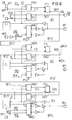
- FIG. 7 shows a variant of a testable circuit module, in which a previously common controller COT is provided. This controls all integrated circuits IC1, IC2, IC3 and therefore only has to be present once. As before, the control information TMI can be entered serially into the controller in the case of conventional testable assemblies, thereby saving one or two test points (in the case of bidirectional test stages).
Abstract
Description
Die Erfindung betrifft Schaltungsbaugruppen und integrierte Schaltungen für das sogenannte Boundary-Scan-Prüfverfahren.The invention relates to circuit modules and integrated circuits for the so-called boundary scan test method.
Bei diesem Prüfverfahren weisen die integrierten Schaltungen an logischen Eingängen und logischen Ausgängen Prüfstufen (Boundary Scan cells) auf, die zwischen den Anschlußpunkten und der Funktionslogik angeordnet sind. Die Eingangsprüfstufen und die Ausgangsprüfstufen bilden eine Schieberegisterkette um den logischen Baustein (seine Grenze = Boundary) herum. Da in der Regel mehrere integrierte Schaltkreise auf einer Baugruppe angeordnet sind, werden ihre Prüfstufen in Kette geschaltet. Das Boundary-Scan-Prüfverfahren ist in der Zeitschrift Elektronik in einer Fortsetzungs-Artikelserie in den Heften 12 (Seiten 52-57) / 13 (Seiten 102-108) / 14 (Seiten 96-103 ) / 15 (Seite 69-74) und 17 (Seiten 62-68) 1989 beschrieben.In this test method, the integrated circuits at logic inputs and logic outputs have test stages (boundary scan cells) which are arranged between the connection points and the functional logic. The input test stages and the output test stages form a shift register chain around the logic module (its boundary = boundary). Since several integrated circuits are usually arranged on one module, their test stages are connected in a chain. The Boundary-Scan test method is published in the magazine "Elektronik" in a series of articles in booklets 12 (pages 52-57) / 13 (pages 102-108) / 14 (pages 96-103) / 15 (pages 69-74) and 17 (pages 62-68) 1989.
In Heft 17, S. 67, Bild 5 ist eine Baugruppe mit zwei integrierten Schaltungen dargestellt und das Prüfverfahren im Begleittext beschrieben. Mit diesem Prüfverfahren lassen sich vor allen Dingen die Verbindungsleitungen von der Steckerleiste der Baugruppe zu den Anschlüssen der integrierten Bausteine und zwischen den integrierten Bausteinen überprüfen; ebenso können die Funktionen der logische Bausteine überprüft werden. Das Boundary-Scan-Verfahren hat den Vorteil, daß nur wenige zusätzliche Anschlußpunkte bei den integrierten Schaltungen und auf der Baugruppe vorgesehen werden müssen. In Heft 14, Seite 97, Bild 2 ist die Anordnung der Prüfstufen (Scope ≙ boundary- scan cell) dargestellt. Für Testzwecke können die Prüfzellen gesteuert werden. Diese Steuerung erfolgt über eine mit JTAG-Control bezeichnete Steuereinrichtung, die aus einem seriellen Steuersignal TMS mehrere parallele Steuersignale erzeugt. Dies hat den Vorteil, daß insgesamt nur vier zusätzliche Anschlußpunkte: für die eingegebene Prüfinformation TDI, die ausgegebene Prüfinformation TDO, für die Steuerinformation TMS und den Prüftakt TC benötigt werden. Im IEEE Standard 1149.1 "Standard Test Access, Port and Boundary-Scan Architecture, November 25, 1988" wurden bereits Bedingungen für die Durchführung des Test und Schaltungen für die Testlogik vorgeschlagen. Hier sind auch Eingangsprüfzellen (S. 8-7 und 8-8 ) und Ausgangsprüfzellen (S. 8-9 und 8-11) sowie auch Prüfzellen für Tri-State-Anschlüsse (S. 8-13) vorgeschlagen. Verwendet wurden bisher meist kompliziertere Prüfstufen, die eine weitgehend unabhängige Handhabung der seriell eingegebenen Prüfinformation von den an den Ein- und Ausgängen der integrierten Schaltkreise anliegenden logischen Zuständen ermöglicht. Diese Prüfstufen haben jedoch den Nachteil, daß sie relativ aufwendig sind und in den Signalwegen liegen. Außerdem ist in jedem Baustein eine Steuerung erforderlich, die einen erheblichen zusätzlichen Schaltungsaufwand mit sich bringt.Issue 17, p. 67, Figure 5 shows an assembly with two integrated circuits and the test procedure is described in the accompanying text. Above all, this test procedure can be used to check the connecting cables from the connector strip of the module to the connections of the integrated modules and between the integrated modules; the functions of the logical blocks can also be checked. The boundary scan method has the advantage that only a few additional connection points have to be provided for the integrated circuits and on the module. Book 14, page 97, Figure 2 shows the arrangement of the test levels (scope ≙ boundary scan cell). The test cells can be controlled for test purposes. This control takes place via a control device designated JTAG-Control, which consists of a serial control signal TMS generates several parallel control signals. This has the advantage that only four additional connection points are required: for the entered test information TDI, the output test information TDO, for the control information TMS and the test clock TC. In IEEE Standard 1149.1 "Standard Test Access, Port and Boundary-Scan Architecture, November 25, 1988", conditions for carrying out the test and circuits for the test logic have already been proposed. Input test cells (p. 8-7 and 8-8) and output test cells (p. 8-9 and 8-11) as well as test cells for tri-state connections (p. 8-13) are also proposed here. So far, mostly more complicated test stages have been used, which allow largely independent handling of the test information entered serially from the logic states present at the inputs and outputs of the integrated circuits. However, these test stages have the disadvantage that they are relatively complex and lie in the signal paths. In addition, a controller is required in each module, which entails considerable additional circuitry.
Aufgabe der Erfindung ist es daher, integrierte Schaltungen und Baugruppen für das Boundary-Scan-Prüfverfahren anzugeben, die ein Testen mit einer maximalen Geschwindigkeit ermöglichen und bei denen der zusätzlichen Schaltungsaufwand auf ein Minimum reduziert ist.The object of the invention is therefore to provide integrated circuits and assemblies for the boundary scan test method, which enable testing at maximum speed and in which the additional circuit complexity is reduced to a minimum.
Die in den unabhängigen Ansprüchen angegebenen integrierten Schaltkreise benötigen nur einen minimalen Schaltungsmehraufwand für Prüfzwecke und weisen in den Datenleitungen nur eine minimale Anzahl von zusätzlichen Schaltungselementen auf.The integrated circuits specified in the independent claims require only minimal additional circuitry for test purposes and have only a minimal number of additional circuit elements in the data lines.
In den Verbindungsleitungen zwischen Eingangs-Anschlußpunkten und Funktionslogik einer integrierten Schaltung wird kein weiteres Schaltungselement eingefügt. Die Prüfstufen werden zweckmäßigerweise nach der Bond-Verbindung angeschaltet. Schutzschaltungen oder Trennverstärker können hierbei noch vor der Eingangs-Prüfstufe liegen. Ebenso kann die Ausgangs-Prüfstufe noch vor einem Ausgangsverstärker oder/und Schutzschaltungen angebracht sein. In der Ausgangs-Verbindungsleitung liegt nur ein einziger Multiplexer, so daß die Signallaufzeit nur geringfügig verzögert wird. Die Speicherstufen der Ausgangs-Prüfstufen sind direkt ohne weitere Logikelemente zu einem Schieberegister zusammengeschaltet.No further circuit element is inserted in the connecting lines between input connection points and functional logic of an integrated circuit. The test stages are expediently switched on after the bond connection. Protective circuits or isolating amplifiers can be located before the input test stage. Likewise, the output test stage can still be installed before an output amplifier and / or protective circuits. There is only a single multiplexer in the output connecting line, so that the signal delay is only slightly delayed. The memory stages of the output test stages are directly connected to a shift register without any further logic elements.
Besonders vorteilhaft ist die getrennte Steuerung der Multiplexer der Eingangs-Prüfstufen und der Ausgangs-Prüfstufen. Eine Steuerung (Controller) wird in der integrierten Schaltung dann nicht benötigt, da die Information an den Datenausgängen der Ausgangs-Prüfstufen ständig entsprechend dem Prüfdatensignal TDI wechselt, wird durch eine Trennung der Steuerleitungen bzw. der Steuersignale für die eingangsseitige und ausgangsseitige Schieberegisterkette erreicht, daß wahlweise nur die von der Funktionslogik ausgegebenen Daten an den Ausgängen der Ausgangs-Prüfstufen und damit der Anschlußpunkte des integrierten Bausteines angegeben werden.The separate control of the multiplexers of the input test stages and the output test stages is particularly advantageous. A controller is then not required in the integrated circuit, since the information at the data outputs of the output test stages changes continuously in accordance with the test data signal TDI, by separating the control lines or the control signals for the input-side and output-side shift register chain, that is achieved Optionally, only the data output by the function logic can be specified at the outputs of the output test stages and thus the connection points of the integrated module.
Bei bidirektionalen Anschlüssen der integrierten Bausteine wird eine Kombination der verwendeten Eingangs-Prüfstufen und Ausgangs-Prüfstufen verwendet. Diese weisen zusätzlich noch einen Steuerteil auf, um ebenfalls die Richtung des Datenflusses über eine Tri-State-Ausgangsstufe steuern zu können. Hierzu ist allerdings ein weiterer Anschlußpunkt der integrierten Schaltung erforderlich. Bei einem Datenbus werden die zugehörigen Ausgangsstufen durch einen gemeinsamen Steuerteil gesteuert.A combination of the input test stages and output test stages used is used for bidirectional connections of the integrated modules. These also have a control section so that the direction of the data flow can also be controlled via a tri-state output stage. However, an additional connection point of the integrated circuit is required for this. In the case of a data bus, the associated output stages are controlled by a common control section.
Vorteilhaft ist es, wenn beide Steuerleitungen auch auf die Steckerleiste oder eine separate Prüfsteckerleiste der Baugruppe herausgeführt wird. Auf die eine Steuerung (Controller) auf der Baugruppe kann dann verzichtet werden. Selbstverständlich kann auch der bisher benötigte Controller auf der Baugruppe wieder eingesetzt werden, der dann den Prüfvorgang bei allen integrierten Bausteinen steuert. Hierdurch wird ein Anschlußpunkt bzw. zwei Anschlußpunkte bei der Baugruppe eingespart.It is advantageous if both control lines are also led out to the connector strip or a separate test connector strip of the module. One controller on the module can then be dispensed with. Of course, the previously required controller can also be used on the module, which then controls the test process for all integrated modules. This saves one connection point or two connection points in the assembly.
Vorteilhafte Ausbildungen der Erfindung sind in den übrigen Unteransprüchen angegeben.Advantageous developments of the invention are specified in the remaining subclaims.
Ausführungsbeispiele der Erfindung werden anhand von Figuren näher erläutert.Embodiments of the invention are explained in more detail with reference to figures.
Es zeigen:
- Fig. 1
- eine integrierte Schaltung auf einer Baugruppe,
- Fig. 2
- eine Eingangs-Prüfstufe,
- Fig. 3
- eine Ausgangs-Prüfstufe,
- Fig. 4
- ein Verdrahtungsschema für die Prüfstufen,
- Fig. 5
- eine Prüfstufe für bidirektionelle Anschlüsse,
- Fig. 6
- ein Verdrahtungsschema für diese Prüfstufen und
- Fig. 7
- eine Baugruppe mit einem Controller.
- Fig. 1
- an integrated circuit on an assembly,
- Fig. 2
- an entrance test level,
- Fig. 3
- an exit test level,
- Fig. 4
- a wiring diagram for the test levels,
- Fig. 5
- a test level for bidirectional connections,
- Fig. 6
- a wiring diagram for these test levels and
- Fig. 7
- an assembly with a controller.
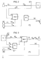
In Figur 1 ist eine integrierte Schaltung IC auf einer Baugruppe BG dargestellt. Der integrierte Baustein IC weist eine Funktionslogik FL auf, in der die logischen Verknüpfungen hergestellt werden, die zur Realisierung einer gewünschten Funktion erforderlich sind. Bei der Funktionslogik kann es sich sowohl um eine Verknüpfung von logischen Gattern handeln, ebenso kann es sich um eine Verknüpfung von Speicherstufen mit Gattern, um reine Speicherstufen oder auch um Mikroprozessoren und so weiter handeln. Zwischen den Eingangs-Anschlußpunkten (pins) EP1, EP2, ... EPn des integrierten Bausteines und Eingängen der Funktionslogik sind Eingangs-Prüfstufen (scan input cells) EPS1 bis EPSn angeschaltet. Ebenso sind zwischen Ausgängen der Funktionslogik FL und Ausgangs-Anschlußpunkten AP1 bis APf Ausgangs-Prüfstufen (scan output cells) APS1 bis APSf eingeschaltet. Die Stufen der Speicherstufen EPS1 bis APSf sind in Kette schaltbar und bilden dann ein Schieberegister. Der ersten Eingangs-Prüfstufe EPS1 wird ein Prüfdatensignal TDI über einen Prüfdaten-Eingang TDE zugeführt. Die Prüfdaten können sämtliche Prüfstufen durchlaufen und beispielsweise unverändert am Prüfdatenausgang TDA der letzten Ausgangs-Prüfstufe APSf als Ausgangs-Prüfdatensignal TDO ausgegeben werden. In den Prüfstufen werden die Prüfdaten mit einem Prüftaktsignal TC getaktet. Die Eingangs-Prüfstufen und die Ausgangs-Prüfstufen sind über Steuersignale MS1 bzw. MS2 separat steuerbar.1 shows an integrated circuit IC on an assembly BG. The integrated module IC has a functional logic FL, in which the logical connections are established which are required to implement a desired function. The functional logic can be a combination of logic gates, it can also be a combination of memory stages with gates, pure memory stages or also microprocessors and so on. Input test stages (scan input cells) EPS1 to EPSn are connected between the input connection points (pins) EP1, EP2, ... EPn of the integrated module and inputs of the function logic. Output test stages (scan output cells) APS1 to APSf are likewise switched on between outputs of the functional logic FL and output connection points AP1 to APf. The stages of the memory stages EPS1 to APSf can be switched in a chain and then form a shift register. A test data signal TDI is fed to the first input test stage EPS1 via a test data input TDE. The test data can run through all test stages and, for example, can be output unchanged at the test data output TDA of the last output test stage APSf as the output test data signal TDO. In the test stages, the test data are clocked with a test clock signal TC. The input test stages and the output test stages can be controlled separately via control signals MS1 or MS2.
In Figur 2 ist eine Eingangs-Prüfstufe EPS detailliert dargestellt. Ein Eingangs-Anschlußpunkt (pin) EP ist direkt mit der Funktionslogik FL über eine Verbindungsleitung ESL verbunden. An diese Verbindungsleitung (nach der Bondleitung und gegebenenfalls Schutzschaltungen oder/und Eingangspuffern) ist der erste Eingang A1 eines Eingangs-Multiplexers MUX1 angeschaltet. Über diesen Eingang können Eingangsdaten ED an den Multiplexerausgang durchgschaltet werden. Der zweite Multiplexereingang B1 stellt den Dateneingang DE1 für das Prüfdatensignal TDI dar. Der Ausgang des Multiplexers ist mit dem Dateneingang einer Eingangs-Speicherstufe FF1, beispielsweise einer D-Kippstufe, verbunden. Ein Ausgang dieser Kippstufe stellt den Datenausgang DA1 dar. Der Eingangs-Multiplexer wird über eine erste Steuerleitung ST1 von einem an einem ersten Steuereingang ME1 anliegenden Eingangsmode-Steuersignal MS1 gesteuert, so daß wahlweise der Anschlußpunkt EP (MS1 = log. 0) oder der Dateneingang DE1 (MS1 = log. 1) auf den Dateneingang der Eingangs-Speicherstufe FF1 schaltbar ist. Der Eingangs-Speicherstufe FF1 wird außerdem das Prüftaktsignal TC über einen Takteingang TE zugeführt. Der Datenausgang DA1 der ersten Eingangs-Prüfstufe wird mit dem Dateneingang DE1 (DE12) der zweiten Prüfstufe verbunden und so weiter, wie dies aus Figur 4 entnehmbar ist. Die Dateneingänge und Datenausgänge sind entsprechend der Nummerierung der Eingangs-Prüfstufen mit einer weiteren Ziffer versehen.An input test stage EPS is shown in detail in FIG. An input connection point (pin) EP is connected directly to the functional logic FL via a connecting line ESL. The first input A1 of an input multiplexer MUX1 is connected to this connecting line (after the bond line and, if appropriate, protective circuits and / or input buffers). Input data ED can be switched through to the multiplexer output via this input. The second multiplexer input B1 represents the data input DE1 for the test data signal TDI. The output of the multiplexer is connected to the data input of an input memory stage FF1, for example a D flip-flop. An output of this flip-flop represents the data output DA1. The input multiplexer is controlled via a first control line ST1 by an input mode control signal MS1 present at a first control input ME1, so that either the connection point EP (MS1 = log. 0) or the data input DE1 (MS1 = log. 1) can be switched to the data input of the input memory stage FF1. The input clock stage FF1 is also supplied with the test clock signal TC via a clock input TE. The data output DA1 of the first input test stage is connected to the data input DE1 (DE12) of the second test stage and so on, as can be seen in FIG. 4. The data inputs and data outputs are provided with a further number in accordance with the numbering of the input test stages.
Bevor auf die Funktion der Eingangs-Prüfstufen näher eingegangen wird, soll erst eine Ausgangs-Prüfstufe beschrieben werden.Before the function of the input test stages is discussed in more detail, an output test stage should first be described.
In Figur 3 ist eine Ausgangs-Prüfstufe APS dargestellt. Die Funktionslogik FL ist mit einem ersten Eingang A2 eines Ausgangs-Multiplexers MUX2 verbunden, dessen Ausgang auf einen Ausgangs-Anschlußpunkt (pin) AP geführt ist. Einem zweiten Eingang B2 des Ausgangs-Multiplexers MUX2 ist eine Ausgangs-Speicherstufe FF2 vorgeschaltet, deren Dateneingang mit DE2 und deren Datenausgang mit DA2 bezeichnet ist. Die Ausgangs-Speicherstufe wird ebenfalls von dem Prüftaktsignal TC getaktet.An output test stage APS is shown in FIG. The functional logic FL is connected to a first input A2 of an output multiplexer MUX2, the output of which is led to an output connection point (pin) AP. An output memory stage FF2 is connected upstream of a second input B2 of the output multiplexer MUX2, the data input of which is designated DE2 and the data output of which is designated DA2. The output memory stage is also clocked by the test clock signal TC.
Über einen zweiten Steuereingang ME2 und eine zweite Steuerleitung ST2 ist der Ausgangs-Multiplexer MUX2 durch ein Ausgangsmode-Steuersignal MS2 umschaltbar. Wahlweise können Ausgangsdaten AD von der Funktionslogik FL (MS2 = log. 0) oder das Prüfdatensignal TDO (MS2 = log. 1) an den Ausgangs-Anschlußpunkt AP durchgeschaltet werden. In die Verbindungsleitung ASL zwischen Funktionslogik FL und Ausgangs-Anschlußpunkt AP ist nur der Ausgangs-Multiplexers MUX2 zusätzlich eingeschaltet. Natürlich kann auch noch ein Ausgangsverstärker (Buffer) oder eine Schutzschaltung zwischen dem Ausgang des Ausgangs-Multiplexers und dem Anschlußpunkt bzw. der Bondleitung eingeschaltet sein.Via a second control input ME2 and a second control line ST2, the output multiplexer MUX2 can be switched over by an output mode control signal MS2. Output data AD from the function logic FL (MS2 = log. 0) or the test data signal TDO (MS2 = log. 1) can optionally be switched through to the output connection point AP. Only the output multiplexer MUX2 is additionally switched on in the connecting line ASL between the functional logic FL and the output connection point AP. Of course, an output amplifier (buffer) or a protective circuit can also be connected between the output of the output multiplexer and the connection point or the bond line.
Der Dateneingang DE2 der ersten Ausgangs-Prüfstufe ist an den Datenausgang DA1 (DA1n in Fig. 4) der letzten Eingangs-Prüfstufe EPSn angeschaltet. Bei den übrigen Ausgangs-Prüfstufen ist jeweils ein Dateneingang DE2 der folgenden Ausgangs-Prüfstufe an den Datenausgang DA2 der vorhergehenden Ausgangs-Prüfstufe angeschlossen, wie dies ebenfalls aus Figur 4 hervorgeht. Auch hier sind entsprechend der Nummerierung der Ausgangs-Prüfstufen die Dateneingänge und Datenausgänge jeweils mit einer zweiten Ziffer versehen.The data input DE2 of the first output test stage is connected to the data output DA1 (DA1n in FIG. 4) of the last input test stage EPSn. In the other output test stages, a data input DE2 of the following output test stage is connected to the data output DA2 of the previous output test stage, as can also be seen in FIG. 4. Here, too, the data inputs and data outputs are each provided with a second digit in accordance with the numbering of the output test stages.
Aus Figur 4 ist in Verbindung mit den Figuren 2 und 3 ersichtlich, daß die Eingangs-Speicherstufe FF1 der letzten Eingangs-Prüfstufe oder die Ausgangs-Speicherstufe FF2 der ersten Ausgangs-Prüfstufe entfallen kann.It can be seen from FIG. 4 in connection with FIGS. 2 and 3 that the input memory stage FF1 of the last input test stage or the output memory stage FF2 of the first output test stage can be omitted.
Die Speicherstufen FF1 der Eingangs-Prüfstufen können einmal die an den Eingangs-Anschlußpunkten EP anliegende Eingangs-Information ED parallel übernehmen.The memory stages FF1 of the input test stages can take over the input information ED present at the input connection points EP in parallel.
Diese kann dann durch Bildung eines Schieberegisters durch Steuerung über das Eingangsmode-Steuersignal MS1 über die Ausgangs-Speicherstufen FF2 der Ausgangsprüfstufen seriell ausgegeben und ausgewertet werden.This can then be serially output and evaluated by forming a shift register by control via the input mode control signal MS1 via the output memory stages FF2 of the output test stages.
Durch Anlegen von 01-Folgen an die Eingangs-Anschlußpunkte EP werden die Verbindungsleitungen auf Unterbrechung und Kurzschluß überprüft.By connecting 01 sequences to the input connection points EP, the connecting lines are checked for interruptions and short circuits.
Über den Prüfdateneingang TDE können beliebige Prüfdaten TDI über die Eingangs-Prüfstufen in die Speicherstufen FF2 der Ausgangs-Prüfstufen eingegeben werden. Diese bilden immer ein Ausgangs-Schieberegister, dessen durchgeschobene Information stets am Prüfdatenausgang TDA seriell ausgegeben wird. Die Ausgangs-Prüfinformation ist mit TDO bezeichnet; sie kann mit dem durchgeschobenen Prüfdatensignal TDI übereinstimmen aber auch, wie vorstehend beschrieben, durch die Eingangsdaten ED gebildet werden.Any test data TDI can be entered via the input test stages into the memory stages FF2 of the output test stages via the test data input TDE. These always form an output shift register, the shifted information of which is always output serially at the test data output TDA. The output test information is designated TDO; it can coincide with the test data signal TDI being pushed through, but, as described above, can also be formed by the input data ED.
Über die Eingangs-Anschlußpunkte EP können unterschiedliche Eingangskombinationen an die integrierte Schaltung und damit an die Eingänge der Funktionslogik FL angelegt werden, deren Funktion anhand der an den Ausgangs-Anschlußpunkten AP abgegebenen Ausgangsdaten AD überprüft wird. Sind die Ausgangs-Anschlußpunkte auf die Steckerleiste der Baugruppe geführt, ist hier auch eine Überprüfung direkt möglich. Sind die Ausgangs-Anschlußpunkte AP des integrierten Bausteines dagegen auf Eingänge eines oder mehrerer integrierter Bausteine geführt, so können die anliegenden logischen Daten wiederum über deren Eingangs- und Ausgangs-Prüfschaltungen getestet werden.Via the input connection points EP, different input combinations can be applied to the integrated circuit and thus to the inputs of the functional logic FL, the function of which is checked on the basis of the output data AD output at the output connection points AP. If the output connection points are routed to the module's connector strip, a check can also be carried out here directly. If, on the other hand, the output connection points AP of the integrated module are routed to inputs of one or more integrated modules, the logic data present can in turn be tested via their input and output test circuits.
Die Ausgangs-Prüfdaten TDO werden vom Ausgang der Speicherstufe FF1 der letzten Eingangsprüfstufe ständig in das Ausgangs-Schieberegister (alle Speicherstufen FF2) übernommen und ausgegeben. Wenn die Ausgangs-Multiplexer MUX2 die Ausgangsdaten AD durchschalten, stören sie jedoch nicht. So kann die Funktionslogik überprüft werden und gleichzeitig können bereits Prüfdaten in das Ausgangs-Schieberegister übernommen werden.The output test data TDO are continuously transferred from the output of the memory stage FF1 of the last input test stage to the output shift register (all memory stages FF2) and output. However, when the output multiplexers MUX2 switch through the output data AD, they do not interfere. In this way the functional logic can be checked and test data can already be transferred to the output shift register.
Diese werden zum Überprüfen der angeschlossenen Leitungen auf die Ausgangs-Anschlußpunkte AP durchgeschaltet. Sind diese mit Anschlußpunkten der Steckerleiste der Baugruppe verbunden, können sie direkt überprüft werden, sonst müssen - wie bei der Überprüfung der Funktionslogik - sie über die Eingangs-Prüfstufe der angeschlossenen Bausteine in die Eingangs-Speicherstufen FF1 zunächst eingelesen und nach der Ausgabe des Prüfdatensignals TDO bewertet werden. Wenn als Prüfdateninformation TDI eine 0101-Folge, 0011-Folge usw. gewählt wird, können auch an den Ausgangs-Anschlußpunkten AP angeschaltete analoge Bauelemente, beispielsweise Übertrager mit überprüft werden.These are switched through to check the connected lines to the output connection points AP. If these are connected to connection points of the connector strip of the module, they can be checked directly, otherwise - as with the function logic check - they must first be read into the input memory stages FF1 via the input test stage of the connected modules and after the test data signal TDO has been output be rated. If a 0101 sequence, 0011 sequence, etc. is selected as the test data information TDI, analog components, for example transformers, connected to the output connection points AP can also be checked.
Bei den gewählten Eingangs-Prüfstufen ist es nicht möglich, beliebige Prüfdaten TDI über den Prüfdateneingang TDE an die Eingangs-Anschlußpunkte ED anzulegen. Sie eignen sich daher besonders zur Überprüfung der Verbindungsleitungen auf der Baugruppe und der Lötstellen der integrierten Schaltungen.With the selected input test levels, it is not possible to create any test data TDI via the test data input TDE at the input connection points ED. They are therefore particularly suitable for checking the connecting cables on the module and the solder joints of the integrated circuits.
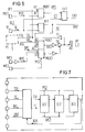
In Figur 5 ist eine Prüfstufe für bidirektionale Anschlußpunkte BP dargestellt. Sie ist eine Kombination aus Eingangs-Prüfstufe und Ausgangs-Prüfstufe. Deshalb sind die Bezeichnungen für die Bauelemente, die Dateneingänge und Datenausgänge beibehalten worden. Der Eingangsteil ET mit dem Eingangs-Multiplexer MUX1 und der Eingangs-Speicherstufe FF1 entspricht einer Eingangs-Prüfstufe; der Ausgangsteil AT mit der Ausgangs-Prüfstufe FF2 und dem Ausgangs-Multiplexer MUX2 entspricht einer Ausgangs-Prüfstufe. Der Datenausgang DM2 dieses Multiplexers ist über eine Tri-State-Stufe TB auf den Anschlußpunkt BP geführt, der über einen Trennverstärker TS mit der Verbindungsleitung ESL der Funktionslogik FL und dem ersten Eingang A1 des Eingangs-Multiplexers MUX1 verbunden ist. Wie bisher ist eine Ausgangs-Verbindungsleitung ASL mit dem ersten Eingang des Ausgangs-Multiplexers MUX2 (≙ dem Ausgangs-Multiplexers MUX2 einer Ausgangs-Prüfstufe) verbunden. Ein dritter Multiplexer MUX3 arbeitet als Steuerteil, das die Tri-State-Stufe TB aktiv oder hochohmig schaltet. Dem ersten Eingang A3 dieses Multiplexers wird ein Richtungssignal DRS von der Funktionslogik zugeführt, während an dem zweiten Eingang B3 über einen dritten Steuereingang MP3 ein externes Richtungssignal BMS anliegt. Die Multiplexer MUX2 und MUX3 werden durch das Ausgangs-Mode-Steuersignal MS2 geschaltet. Bei normalem Betrieb (MS2 = log. 1) erfolgt die Richtungssteuerung durch das Datenrichtungssignal DRS der Funktionslogik FL. Werden dagegen die in den Ausgangs-Speicherstufen FF2 vorhandenen Daten über den Ausgangs-Multiplexer MUX2 durchgeschaltet (MS2 = log. 0) so erfolgt die Richtungssteuerung über das externe Richtungssignal BMS (z.B. BMS = log. 1: TB auf Tri-State). Durch die getrennten Eingangsmode- und Ausgangsmode-Steuersignale MS1 und MS2 sind wiederum alle Prüfmöglichkeiten gegeben.FIG. 5 shows a test stage for bidirectional connection points BP. It is a combination of an input test level and an output test level. The designations for the components, the data inputs and data outputs have therefore been retained. The input part ET with the input multiplexer MUX1 and the input memory stage FF1 corresponds to an input test stage; the output part AT with the output test stage FF2 and the output multiplexer MUX2 corresponds to an output test stage. The data output DM2 of this multiplexer is routed via a tri-state stage TB to the connection point BP, which is connected via a isolating amplifier TS to the connecting line ESL of the functional logic FL and to the first input A1 of the input multiplexer MUX1. As before, an output connection line ASL is connected to the first input of the output multiplexer MUX2 (≙ the output multiplexer MUX2 of an output test stage). A third multiplexer MUX3 works as a control part, the tri-state stage TB is active or high-resistance switches. A direction signal DRS is supplied to the first input A3 of this multiplexer by the functional logic, while an external direction signal BMS is applied to the second input B3 via a third control input MP3. The multiplexers MUX2 and MUX3 are switched by the output mode control signal MS2. In normal operation (MS2 = log. 1) the direction is controlled by the data direction signal DRS of the function logic FL. If, on the other hand, the data available in the output memory stages FF2 are switched through via the output multiplexer MUX2 (MS2 = log. 0), the direction is controlled via the external direction signal BMS (eg BMS = log. 1: TB on tri-state). The separate input mode and output mode control signals MS1 and MS2 in turn provide all test options.
In Figur 6 ist die Verdrahtung von bidirektionalen Prüfstufen dargestellt. Die Verdrahtung der Eingangsteile ET1 bis ETn erfolgt in der üblichen Weise, bei der der Datenausgang DA11 des ersten Eingangsteils ET1 mit dem Dateneingang DE12 des zweiten Eingangsteils verbunden ist usw. Der Datenausgang DA1n des letzten Eingangsteiles ETn ist mit dem Dateneingang DE21 des ersten Ausgangsteiles AT1 verbunden. Dieser kann im Prinzip beliebig gewählt werden und ebenso in der ersten bidirektionalen Prüfstufe BPS1 als auch in der letzten bidirektionalen Prüfstufe BPSn positioniert sein, wie dies in Figur 6 der Fall ist. Ein Datenausgang DA2 eines Ausgangsteils AT1 wird mit dem Dateneingang DE22 des nächsten Ausgangsteils AT2 verbunden und so weiter bis der Datenausgang DA2n auf dem Prüfdatenausgang TDA der integrierten Schaltung geführt wird. Funktionsmäßig entspricht die bidirektionale Prüfstufe einer Eingangs- und einer Ausgangsprüfstufe, davon abgesehen, daß über einen Anschlußpunkt Daten nur eingegeben oder ausgegeben werden können. In der Regel sind bidirektionale Anschlußpunkte und zumindest Eingangs-Anschlußpunkte auf einen IC vorhanden. In einem solchen Fall können unterschiedliche Prüfstufen verwendet werden. Ebenso können bipolare Prüfstufen nur teilweise funktionell genutzt werden. Eingangs-Prüfstufen, Ausgangs-Prüfstufen und bidirektionale Prüfstufen (deren Eingangsteile und Ausgangsteile) können in Kette geschaltet werden.FIG. 6 shows the wiring of bidirectional test stages. The input parts ET1 to ETn are wired in the usual way, in which the data output DA11 of the first input part ET1 is connected to the data input DE12 of the second input part, etc. The data output DA1n of the last input part ETn is connected to the data input DE21 of the first output part AT1 . In principle, this can be chosen arbitrarily and can also be positioned in the first bidirectional test stage BPS1 and also in the last bidirectional test stage BPSn, as is the case in FIG. 6. A data output DA2 of an output part AT1 is connected to the data input DE22 of the next output part AT2 and so on until the data output DA2n is routed to the test data output TDA of the integrated circuit. Functionally, the bidirectional test level corresponds to an input and an output test level, apart from the fact that data can only be input or output via a connection point. As a rule, there are bidirectional connection points and at least input connection points on an IC. In such a case, different test levels can be used. Likewise, bipolar test levels can only be partially used functionally. Input test levels, output test levels and bidirectional test stages (their input parts and output parts) can be switched in a chain.
In Figur 7 ist eine Variante einer prüfbaren Schaltungsbaugruppe dargestellt, bei der ein bisher üblicher Controller COT vorgesehen ist. Dieser steuert sämtliche integrierten Schaltungen IC1, IC2, IC3 und muß daher nur einmal vorhanden sein. Die Steuerinformation TMI kann wie bisher bei herkömmlichen prüfbaren Baugruppen seriell in den Controller eingegeben werden, wodurch ein oder zwei Prüfpunkte (bei bidirektionalen Prüfstufen) eingespart werden.FIG. 7 shows a variant of a testable circuit module, in which a previously common controller COT is provided. This controls all integrated circuits IC1, IC2, IC3 and therefore only has to be present once. As before, the control information TMI can be entered serially into the controller in the case of conventional testable assemblies, thereby saving one or two test points (in the case of bidirectional test stages).
Claims (7)
und bei der zwischen der Funktionslogik (FL) und den Ausgangs-Anschlußpunkten (AP; AP1, AP2,...) jeweils eine Ausgangs-Prüfschaltung (APS; APS1, APS2,...) angeordnet ist, die einen Ausgangs-Multiplexer (MUX2) aufweist, der in die Verbindungsleitung (ASL) zum Ausgangs-Anschlußpunkt (AP) eingeschaltet ist,
dadurch gekennzeichnet,
daß dem zweiten Eingang (DE2) des Ausgangs-Multiplexers (MUX2) eine Ausgangs-Speicherstufe (FF2) vorgeschaltet ist,
deren Dateneingang (DE2) an den Datenausgang (DA2) der letzten Eingangs-Prüfstufe (EPSn) oder bei den weiteren Ausgangs-Prüfstufen (APS2, APS3,...) an den Datenausgang (DA2; DA21, DA22,...) der vorhergehenden Ausgangs-Prüfstufe (APS1, APS2,...) angeschaltet ist,
und daß getrennte Steuerleitungen (ST1, ST2) für die Eingangs-Multiplexer (MUX1) und die Ausgangs-Multiplexer (MUX2) auf Anschlußpunkte der integrierten Schaltung (IC) herausgeführt sind.Testable integrated circuit (IC), in which an input test stage (EPS; EPS1, EPS2, ...) is arranged between the input connection points (EP1, EP2, ...) and the functional logic (FL). Multiplexer (MUX1) and a downstream input memory stage (FF1), the first input (A1) of the input multiplexer (MUX1) to the connecting line (ESL) between the input connection point (EP; EP1, EP2, ...) and function logic (FL) is switched on and the second input (B1) to a test data input (TDI) or, in the further input test stages (EPS2, EPS3, ...) to the data output (DA1) of the memory stage (FF1) previous input test stage (EPS1, EPS2, ...) is switched on,
and in which an output test circuit (APS; APS1, APS2, ...) is arranged between the function logic (FL) and the output connection points (AP; AP1, AP2, ...), which has an output multiplexer ( MUX2), which is switched on in the connecting line (ASL) to the output connection point (AP),
characterized,
that an output memory stage (FF2) is connected upstream of the second input (DE2) of the output multiplexer (MUX2),
whose data input (DE2) to the data output (DA2) of the last input test stage (EPSn) or in the further output test stages (APS2, APS3, ...) to the data output (DA2; DA21, DA22, ...) of previous output test stage (APS1, APS2, ...) is switched on,
and that separate control lines (ST1, ST2) for the input multiplexers (MUX1) and the output multiplexers (MUX2) are led out to connection points of the integrated circuit (IC).
und deren Eingangsteile (ET) und Ausgangsteile (AT) in Kette geschaltet sind,
dadurch gekennzeichnet,
daß der Anschlußpunkt (BP) an eine Eingangsleitung (ESL) der Funktionslogik (FS) geführt ist,
daß in jeder Prüfstufe (BPS) der Anschlußpunkt (BP) im Eingangsteil (ET) auf einen ersten Eingang (A1) eines Eingangs-Multiplexers (MUX1) geführt ist, dessen Ausgang mit einer ersten Speicherstufe (FF1) verbunden ist, deren Ausgang einen Datenausgang (DA1) bildet,
daß der zweite Eingang (B1) des Eingangs-Multiplexers (MUX1) an den Datenausgang (DA1) des Eingangsteils (ET) der vorhergehenden Eingangs-Prüfstufe (EPS) bzw. an den Testdateneingang (TDE) angeschaltet ist;
daß im Ausgangsteil (AT) eine Ausgangsleitung (ASL) der Funktionslogik (FL) über einen ersten Eingang (A3) eines Ausgangs-Multiplexers (MUX3) und über eine Tri-State-Stufe (TB) auf den Anschlußpunkt (BP) geführt ist,
daß eine Ausgangs-Speicherstufe (FF2) vorgesehen ist, die einen Dateneingang (DE2) und einen Datenausgang (DA2) aufweist, der auf einen zweiten Eingang (B2) des Ausgangs-Multiplexers (MUX2) geführt ist, daß eine gemeinsame Steuerleitung (ST1) für die Eingangs-Multiplexer (MUX1) aller Eingangsteile auf einen Anschlußpunkt (ME1) der integrierten Schaltung (IC) herausgeführt ist, und zwei weitere Steuerleitungen (ST2, ST3) auf Anschlußpunkte (ME2, ME3) der integrierten Schaltung (IC) herausgeführt sind, die über einen Steuerteil (MUX3) die Richtungsumschaltung für Eingangsdaten (ED) und Ausgangsdaten (AD) ermöglichen.Testable integrated circuit (ICT) which has bidirectional connection points (BP) and in which test stages (BPS) are provided between the connection points (BP) and the functional logic (FL), which have an input part (ET) and an output part (AT), which are implemented with multiplexers and clocked memory stages,
and whose input parts (ET) and output parts (AT) are connected in a chain,
characterized by
that the connection point (BP) is connected to an input line (ESL) of the function logic (FS),
that in each test stage (BPS) the connection point (BP) in the input part (ET) is led to a first input (A1) of an input multiplexer (MUX1), the output of which is connected to a first memory stage (FF1), the output of which is a data output (DA1) forms
that the second input (B1) of the input multiplexer (MUX1) is connected to the data output (DA1) of the input part (ET) of the previous input test stage (EPS) or to the test data input (TDE);
that in the output part (AT) an output line (ASL) of the functional logic (FL) is led to the connection point (BP) via a first input (A3) of an output multiplexer (MUX3) and via a tri-state stage (TB),
that an output memory stage (FF2) is provided which has a data input (DE2) and a data output (DA2) which is routed to a second input (B2) of the output multiplexer (MUX2), that a common control line (ST1) for the input multiplexers (MUX1) of all input parts is led out to a connection point (ME1) of the integrated circuit (IC), and two further control lines (ST2, ST3) are led out to connection points (ME2, ME3) of the integrated circuit (IC), which enable the direction change for input data (ED) and output data (AD) via a control part (MUX3).
dadurch gekennzeichnet,
daß bidirektionale Prüfstufen (BPS), Eingangs-Prüfstufen (EPS) oder/und Ausgangs-Prüfstufen (APS) in einem Baustein vorgesehen sind und in Kette schaltbar sind.Testable integrated circuit according to claim 1 and 2,
characterized by
that bidirectional test stages (BPS), input test stages (EPS) and / or output test stages (APS) are provided in one module and can be switched in a chain.
und bei der zwischen der Funktionslogik (FL) und den Ausgangs-Anschlußpunkten (AP; AP1, AP2,...) jeweils eine Ausgangs-Prüfschaltung (APS; APS1, APS2,...) angeordnet ist, die einen Ausgangs-Multiplexer (MUX2) aufweist, der in die Verbindungsleitung (ASL) zum Anschlußpunkt (AP) eingeschaltet ist,
dadurch gekennzeichnet,
daß dem zweiten Eingang (DE2) des Ausgangs-Multiplexers (MUX2) eine Ausgangs-Speicherstufe (FF2) vorgeschaltet ist,
deren Dateneingang (DE2) an den Datenausgang (DA2) der letzten Eingangs-Prüfstufe (EPSn) oder bei den weiteren Ausgangs-Prüfstufen (APS2, APS3,...) an den Datenausgang (DA2; DA21, DA22,...) der vorhergehenden Ausgangs-Prüfstufe (APS1, APS2,...) angeschaltet ist,
und daß getrennte Steuerleitungen (ST1, ST2) für die Eingangs-Multiplexer (MUX1) und die Ausgangs-Multiplexer (MUX2) auf Anschlußpunkte der integrierten Schaltung (IC) herausgeführt sind.Testable circuit assembly (BG) with at least one integrated circuit (IC), in which an input test stage (EPS; EPS1, EPS2, ...) between input connection points (EP1, EP2, ...) and functional logic (FL) is arranged, which has an input multiplexer (MUX1) and a downstream input memory stage (FF1), the first input (A1) of the input multiplexer (MUX1) to the connecting line (ESL) between the input connection point (EP; EP1 , EP2, ...) and function logic (FL) is switched on and the second input (B1) to a test data input (TDI) or in the further input test stages (EPS2, EPS3, ...) to the data output (DA1 ) the memory stage (FF1) of the previous input test stage (EPS1, EPS2, ...) is switched on,
and in which an output test circuit (APS; APS1, APS2, ...) is arranged between the function logic (FL) and the output connection points (AP; AP1, AP2, ...), which has an output multiplexer ( MUX2), which is switched on in the connection line (ASL) to the connection point (AP),
characterized by
that an output memory stage (FF2) is connected upstream of the second input (DE2) of the output multiplexer (MUX2),
whose data input (DE2) to the data output (DA2) of the last input test stage (EPSn) or in the further output test stages (APS2, APS3, ...) to the data output (DA2; DA21, DA22, ...) of previous output test stage (APS1, APS2, ...) is switched on,
and that separate control lines (ST1, ST2) for the input multiplexers (MUX1) and the output multiplexers (MUX2) are led out to connection points of the integrated circuit (IC).
mit mindestens einer integrierten Schaltung (ICT), die bidirektionale Anschlußpunkte (BP) aufweist und bei der zwischen den Anschlußpunkten (BP) und der Funktionslogik (FL) Prüfstufen (BPS) vorgesehen sind, die einen Eingangsteil (ET) und einen Ausgangsteil (AT) aufweisen, und mit Multiplexern und getakteten Speicherstufen realisiert sind,
und deren Eingangsteile (ET) und Ausgangsteile (AT) in Kette geschaltet sind,
dadurch gekennzeichnet,
daß der Anschlußpunkt (BP) an eine Eingangsleitung (ESL) der Funktionslogik (FS) geführt ist,
daß in jeder Prüfstufe (BPS) der Anschlußpunkt (BP) im Eingangsteil (ET) auf einen ersten Eingang (A1) eines Eingangs-Multiplexers (MUX1) geführt ist, dessen Ausgang mit einer ersten Speicherstufe (FF1) verbunden ist, deren Ausgang einen Datenausgang (DA1) bildet,
daß der zweite Eingang (B1) des Eingangs-Multiplexers (MUX1) an den Datenausgang (DA1) des Eingangsteils (ET) der vorhergehenden Eingangs-Prüfstufe (EPS) bzw. an den Testdateneingang (TDE) angeschaltet ist;
daß im Ausgangsteil (AT) eine Ausgangsleitung (ASL) der Funktionslogik (FL) über einen ersten Eingang (A3) eines Ausgangs-Multiplexers (MUX2) und über eine Tri-State-Stufe (TB) auf den Anschlußpunkt (BP) geführt ist,
daß eine Ausgangs-Speicherstufe (FF2) vorgesehen ist, die einen Dateneingang (DE2) und einen Datenausgang (DA2) aufweist, der auf einen zweiten Eingang (B2) des Ausgangs-Multiplexers (MUX2) geführt ist, daß eine gemeinsame Steuerleitung (ST1) für die Eingangs-Multiplexer (MUX1) aller Eingangsteile auf einen Anschlußpunkt (ME1) der integrierten Schaltung (IC) herausgeführt ist, und zwei weitere Steuerleitungen (ST2, ST3) auf Anschlußpunkte (ME2, ME3) der integrierten Schaltung (IC) für Eingangsdaten (ED) und Ausgangsdaten (AD) herausgeführt sind, die über einen Steuerteil die Richtungsumschaltung für Eingangsdaten (ED) und Ausgangsdaten (AD) ermöglichen.Testable circuit assembly (BG), in particular according to claim 1,
With at least one integrated circuit (ICT) which has bidirectional connection points (BP) and in which test stages (BPS) are provided between the connection points (BP) and the functional logic (FL), which have an input part (ET) and an output part (AT) have, and are realized with multiplexers and clocked memory stages,
and whose input parts (ET) and output parts (AT) are connected in a chain,
characterized by
that the connection point (BP) is connected to an input line (ESL) of the function logic (FS),
that in each test stage (BPS) the connection point (BP) in the input part (ET) is led to a first input (A1) of an input multiplexer (MUX1), the output of which is connected to a first memory stage (FF1), the output of which is a data output (DA1) forms
that the second input (B1) of the input multiplexer (MUX1) is connected to the data output (DA1) of the input part (ET) of the previous input test stage (EPS) or to the test data input (TDE);
that in the output part (AT) an output line (ASL) of the functional logic (FL) is led to the connection point (BP) via a first input (A3) of an output multiplexer (MUX2) and via a tri-state stage (TB),
that an output memory stage (FF2) is provided which has a data input (DE2) and a data output (DA2) which is routed to a second input (B2) of the output multiplexer (MUX2), that a common control line (ST1) for the input multiplexers (MUX1) of all input parts is led out to a connection point (ME1) of the integrated circuit (IC), and two further control lines (ST2, ST3) to connection points (ME2, ME3) of the integrated circuit (IC) for input data ( ED) and output data (AD) are brought out, which enable the direction changeover for input data (ED) and output data (AD) via a control part.
dadurch gekennzeichnet,
daß integrierte Schaltungen (IC1, IC2, IC3) vorgesehen sind, die bidirektionale Prüfstufen (BPS), Eingangs-Prüfstufen (EPS) oder/und Ausgangsprüfstufen (APS) aufweisen, die in Kette schaltbar sind.Testable assembly according to claim 4 and claim 5,
characterized by
that integrated circuits (IC1, IC2, IC3) are provided which have bidirectional test stages (BPS), input test stages (EPS) and / or output test stages (APS) which can be switched in a chain.
dadurch gekennzeichnet,
daß ein Controller (COT) vorgesehen ist, dem die Steuerinformation (MI) seriell zugeführt wird und diese in parallele Steuerinformation (MS1, MS2, MS3) umsetzt.Testable assembly according to one of claims 4 to 6,
characterized by
that a controller (COT) is provided, to which the control information (MI) is fed serially and converts this into parallel control information (MS1, MS2, MS3).
Applications Claiming Priority (2)
| Application Number | Priority Date | Filing Date | Title |
|---|---|---|---|
| DE4038323 | 1990-11-30 | ||
| DE4038323 | 1990-11-30 |
Publications (2)
| Publication Number | Publication Date |
|---|---|
| EP0487941A2 true EP0487941A2 (en) | 1992-06-03 |
| EP0487941A3 EP0487941A3 (en) | 1992-08-05 |
Family
ID=6419348
Family Applications (1)
| Application Number | Title | Priority Date | Filing Date |
|---|---|---|---|
| EP19910118772 Ceased EP0487941A3 (en) | 1990-11-30 | 1991-11-04 | Testable integrated circuit and associated circuitry |
Country Status (2)
| Country | Link |
|---|---|
| EP (1) | EP0487941A3 (en) |
| JP (1) | JPH04276570A (en) |
Cited By (1)
| Publication number | Priority date | Publication date | Assignee | Title |
|---|---|---|---|---|
| EP0646803A1 (en) * | 1993-10-04 | 1995-04-05 | Nec Corporation | Semiconductor device having a boundary scan test circuit |
Families Citing this family (1)
| Publication number | Priority date | Publication date | Assignee | Title |
|---|---|---|---|---|
| US6430719B1 (en) * | 1998-06-12 | 2002-08-06 | Stmicroelectronics, Inc. | General port capable of implementing the JTAG protocol |
Citations (3)
| Publication number | Priority date | Publication date | Assignee | Title |
|---|---|---|---|---|
| US4799004A (en) * | 1987-01-26 | 1989-01-17 | Kabushiki Kaisha Toshiba | Transfer circuit for operation test of LSI systems |
| US4894830A (en) * | 1987-01-17 | 1990-01-16 | Nec Corporation | LSI chip with scanning circuitry for generating reversals along activated logical paths |
| EP0358376A2 (en) * | 1988-09-07 | 1990-03-14 | Texas Instruments Incorporated | Integrated test circuit |
-
1991
- 1991-11-04 EP EP19910118772 patent/EP0487941A3/en not_active Ceased
- 1991-11-29 JP JP3315705A patent/JPH04276570A/en not_active Withdrawn
Patent Citations (3)
| Publication number | Priority date | Publication date | Assignee | Title |
|---|---|---|---|---|
| US4894830A (en) * | 1987-01-17 | 1990-01-16 | Nec Corporation | LSI chip with scanning circuitry for generating reversals along activated logical paths |
| US4799004A (en) * | 1987-01-26 | 1989-01-17 | Kabushiki Kaisha Toshiba | Transfer circuit for operation test of LSI systems |
| EP0358376A2 (en) * | 1988-09-07 | 1990-03-14 | Texas Instruments Incorporated | Integrated test circuit |
Cited By (2)
| Publication number | Priority date | Publication date | Assignee | Title |
|---|---|---|---|---|
| EP0646803A1 (en) * | 1993-10-04 | 1995-04-05 | Nec Corporation | Semiconductor device having a boundary scan test circuit |
| US5477493A (en) * | 1993-10-04 | 1995-12-19 | Nec Corporation | Semiconductor device having a boundary scan test circuit |
Also Published As
| Publication number | Publication date |
|---|---|
| EP0487941A3 (en) | 1992-08-05 |
| JPH04276570A (en) | 1992-10-01 |
Similar Documents
| Publication | Publication Date | Title |
|---|---|---|
| DE3709032C2 (en) | ||
| DE69631351T2 (en) | ASIC bus structure based on multiplexers | |
| DE69628034T2 (en) | HIGH IMPEDANCE MODE FOR JTAG | |
| EP0275941B1 (en) | ECL-compatible CMOS input/output circuits | |
| DE3215671C2 (en) | Programmable logic arrangement | |
| DE3521461A1 (en) | PROGRAMMABLE LOGIC CIRCUIT ARRAY | |
| DE10138556C1 (en) | Method for testing input / output drivers of a circuit and corresponding test device | |
| DE102007053128B3 (en) | Electronic device comprises clock change over switch for switching between two clock pulses, so that one of clock pulse is made available as output signal | |
| DE60106300T2 (en) | INPUT / OUTPUT THROUGH TEST MODE CIRCUIT | |
| DE3817143C2 (en) | ||
| EP1430320B1 (en) | Electronic component and method for measuring its qualification | |
| EP1430321B1 (en) | Electronic component | |
| EP0487941A2 (en) | Testable integrated circuit and associated circuitry | |
| DE3923764C1 (en) | ||
| EP1221097B1 (en) | Circuit cell for test pattern generation and test pattern compression | |
| DE10322726A1 (en) | Method and apparatus for improving testability of I / O drivers / receivers | |
| DE60320057T2 (en) | System and method for circuit testing | |
| DE102004059505B4 (en) | Arrangement for testing embedded circuits using test islands | |
| DE10120282B4 (en) | Bus signal holding cell and method | |
| DE69433618T2 (en) | APPARATUS FOR CHECKING THE CONNECTION BETWEEN THE OUTPUT OF A CIRCUIT WITH A FIXED LOGICAL OUTPUT AND THE INPUT OF ANOTHER CIRCUIT | |
| DE3839289C1 (en) | Circuit for the operation of an integrated circuit of which it is a component, optionally in a test operation mode or a functional operation mode | |
| DE10338677B3 (en) | Method for testing a circuit unit to be tested and a test device | |
| EP1440324B1 (en) | Electronic component with output buffer control | |
| EP0597926A1 (en) | Process for testing integrated circuits with at least one logic circuit and testable integrated circuit | |
| DE4223881C2 (en) | Bidirectional digital driver stage with shift register cells used to implement a clock-controlled shift register test architecture (boundary scan) |
Legal Events
| Date | Code | Title | Description |
|---|---|---|---|
| PUAI | Public reference made under article 153(3) epc to a published international application that has entered the european phase |
Free format text: ORIGINAL CODE: 0009012 |
|
| AK | Designated contracting states |
Kind code of ref document: A2 Designated state(s): AT CH DE ES FR GB IT LI NL SE |
|
| PUAL | Search report despatched |
Free format text: ORIGINAL CODE: 0009013 |
|
| AK | Designated contracting states |
Kind code of ref document: A3 Designated state(s): AT CH DE ES FR GB IT LI NL SE |
|
| 17P | Request for examination filed |
Effective date: 19920824 |
|
| 17Q | First examination report despatched |
Effective date: 19950529 |
|
| GRAG | Despatch of communication of intention to grant |
Free format text: ORIGINAL CODE: EPIDOS AGRA |
|
| STAA | Information on the status of an ep patent application or granted ep patent |
Free format text: STATUS: THE APPLICATION HAS BEEN REFUSED |
|
| 18R | Application refused |
Effective date: 19970127 |