EP0488148A2 - Method of manufacturing a MOS-type field-effect transistor - Google Patents
Method of manufacturing a MOS-type field-effect transistor Download PDFInfo
- Publication number
- EP0488148A2 EP0488148A2 EP91120153A EP91120153A EP0488148A2 EP 0488148 A2 EP0488148 A2 EP 0488148A2 EP 91120153 A EP91120153 A EP 91120153A EP 91120153 A EP91120153 A EP 91120153A EP 0488148 A2 EP0488148 A2 EP 0488148A2
- Authority
- EP
- European Patent Office
- Prior art keywords
- etching
- substrate
- oxide film
- cleansing
- dry
- Prior art date
- Legal status (The legal status is an assumption and is not a legal conclusion. Google has not performed a legal analysis and makes no representation as to the accuracy of the status listed.)
- Withdrawn
Links
Images
Classifications
-
- H—ELECTRICITY
- H01—ELECTRIC ELEMENTS
- H01L—SEMICONDUCTOR DEVICES NOT COVERED BY CLASS H10
- H01L21/00—Processes or apparatus adapted for the manufacture or treatment of semiconductor or solid state devices or of parts thereof
- H01L21/02—Manufacture or treatment of semiconductor devices or of parts thereof
- H01L21/04—Manufacture or treatment of semiconductor devices or of parts thereof the devices having at least one potential-jump barrier or surface barrier, e.g. PN junction, depletion layer or carrier concentration layer
- H01L21/18—Manufacture or treatment of semiconductor devices or of parts thereof the devices having at least one potential-jump barrier or surface barrier, e.g. PN junction, depletion layer or carrier concentration layer the devices having semiconductor bodies comprising elements of Group IV of the Periodic System or AIIIBV compounds with or without impurities, e.g. doping materials
- H01L21/30—Treatment of semiconductor bodies using processes or apparatus not provided for in groups H01L21/20 - H01L21/26
-
- H—ELECTRICITY
- H01—ELECTRIC ELEMENTS
- H01L—SEMICONDUCTOR DEVICES NOT COVERED BY CLASS H10
- H01L21/00—Processes or apparatus adapted for the manufacture or treatment of semiconductor or solid state devices or of parts thereof
- H01L21/02—Manufacture or treatment of semiconductor devices or of parts thereof
- H01L21/02041—Cleaning
- H01L21/02043—Cleaning before device manufacture, i.e. Begin-Of-Line process
- H01L21/02054—Cleaning before device manufacture, i.e. Begin-Of-Line process combining dry and wet cleaning steps
-
- H—ELECTRICITY
- H01—ELECTRIC ELEMENTS
- H01L—SEMICONDUCTOR DEVICES NOT COVERED BY CLASS H10
- H01L21/00—Processes or apparatus adapted for the manufacture or treatment of semiconductor or solid state devices or of parts thereof
- H01L21/02—Manufacture or treatment of semiconductor devices or of parts thereof
- H01L21/02041—Cleaning
- H01L21/02043—Cleaning before device manufacture, i.e. Begin-Of-Line process
- H01L21/02046—Dry cleaning only
-
- H—ELECTRICITY
- H01—ELECTRIC ELEMENTS
- H01L—SEMICONDUCTOR DEVICES NOT COVERED BY CLASS H10
- H01L21/00—Processes or apparatus adapted for the manufacture or treatment of semiconductor or solid state devices or of parts thereof
- H01L21/02—Manufacture or treatment of semiconductor devices or of parts thereof
- H01L21/04—Manufacture or treatment of semiconductor devices or of parts thereof the devices having at least one potential-jump barrier or surface barrier, e.g. PN junction, depletion layer or carrier concentration layer
- H01L21/18—Manufacture or treatment of semiconductor devices or of parts thereof the devices having at least one potential-jump barrier or surface barrier, e.g. PN junction, depletion layer or carrier concentration layer the devices having semiconductor bodies comprising elements of Group IV of the Periodic System or AIIIBV compounds with or without impurities, e.g. doping materials
- H01L21/28—Manufacture of electrodes on semiconductor bodies using processes or apparatus not provided for in groups H01L21/20 - H01L21/268
- H01L21/28008—Making conductor-insulator-semiconductor electrodes
- H01L21/28017—Making conductor-insulator-semiconductor electrodes the insulator being formed after the semiconductor body, the semiconductor being silicon
- H01L21/28158—Making the insulator
- H01L21/28167—Making the insulator on single crystalline silicon, e.g. using a liquid, i.e. chemical oxidation
- H01L21/28211—Making the insulator on single crystalline silicon, e.g. using a liquid, i.e. chemical oxidation in a gaseous ambient using an oxygen or a water vapour, e.g. RTO, possibly through a layer
-
- Y—GENERAL TAGGING OF NEW TECHNOLOGICAL DEVELOPMENTS; GENERAL TAGGING OF CROSS-SECTIONAL TECHNOLOGIES SPANNING OVER SEVERAL SECTIONS OF THE IPC; TECHNICAL SUBJECTS COVERED BY FORMER USPC CROSS-REFERENCE ART COLLECTIONS [XRACs] AND DIGESTS
- Y10—TECHNICAL SUBJECTS COVERED BY FORMER USPC
- Y10S—TECHNICAL SUBJECTS COVERED BY FORMER USPC CROSS-REFERENCE ART COLLECTIONS [XRACs] AND DIGESTS
- Y10S148/00—Metal treatment
- Y10S148/017—Clean surfaces
-
- Y—GENERAL TAGGING OF NEW TECHNOLOGICAL DEVELOPMENTS; GENERAL TAGGING OF CROSS-SECTIONAL TECHNOLOGIES SPANNING OVER SEVERAL SECTIONS OF THE IPC; TECHNICAL SUBJECTS COVERED BY FORMER USPC CROSS-REFERENCE ART COLLECTIONS [XRACs] AND DIGESTS
- Y10—TECHNICAL SUBJECTS COVERED BY FORMER USPC
- Y10S—TECHNICAL SUBJECTS COVERED BY FORMER USPC CROSS-REFERENCE ART COLLECTIONS [XRACs] AND DIGESTS
- Y10S148/00—Metal treatment
- Y10S148/053—Field effect transistors fets
-
- Y—GENERAL TAGGING OF NEW TECHNOLOGICAL DEVELOPMENTS; GENERAL TAGGING OF CROSS-SECTIONAL TECHNOLOGIES SPANNING OVER SEVERAL SECTIONS OF THE IPC; TECHNICAL SUBJECTS COVERED BY FORMER USPC CROSS-REFERENCE ART COLLECTIONS [XRACs] AND DIGESTS
- Y10—TECHNICAL SUBJECTS COVERED BY FORMER USPC
- Y10S—TECHNICAL SUBJECTS COVERED BY FORMER USPC CROSS-REFERENCE ART COLLECTIONS [XRACs] AND DIGESTS
- Y10S438/00—Semiconductor device manufacturing: process
- Y10S438/906—Cleaning of wafer as interim step
-
- Y—GENERAL TAGGING OF NEW TECHNOLOGICAL DEVELOPMENTS; GENERAL TAGGING OF CROSS-SECTIONAL TECHNOLOGIES SPANNING OVER SEVERAL SECTIONS OF THE IPC; TECHNICAL SUBJECTS COVERED BY FORMER USPC CROSS-REFERENCE ART COLLECTIONS [XRACs] AND DIGESTS
- Y10—TECHNICAL SUBJECTS COVERED BY FORMER USPC
- Y10S—TECHNICAL SUBJECTS COVERED BY FORMER USPC CROSS-REFERENCE ART COLLECTIONS [XRACs] AND DIGESTS
- Y10S438/00—Semiconductor device manufacturing: process
- Y10S438/909—Controlled atmosphere
-
- Y—GENERAL TAGGING OF NEW TECHNOLOGICAL DEVELOPMENTS; GENERAL TAGGING OF CROSS-SECTIONAL TECHNOLOGIES SPANNING OVER SEVERAL SECTIONS OF THE IPC; TECHNICAL SUBJECTS COVERED BY FORMER USPC CROSS-REFERENCE ART COLLECTIONS [XRACs] AND DIGESTS
- Y10—TECHNICAL SUBJECTS COVERED BY FORMER USPC
- Y10S—TECHNICAL SUBJECTS COVERED BY FORMER USPC CROSS-REFERENCE ART COLLECTIONS [XRACs] AND DIGESTS
- Y10S438/00—Semiconductor device manufacturing: process
- Y10S438/974—Substrate surface preparation
Definitions
- This invention relates to a method of manufacturing a semiconductor device including a very reliable MOS-type field effect transistor (hereinafter called "MOSFET”) by removing metal impurities during cleansing of the surface of a substrate.
- MOSFET MOS-type field effect transistor
- the conventional cleansing process to be performed before forming a gate oxide film is exemplified by the following:
- a gate oxide film is formed by thermal oxidation.
- metal impurities in the oxide film on the substrate surface can be removed by eliminating the oxide film by an HF cleaning solution, while many impurity particles would be stuck on the surface of the substrate only by this cleansing process. Further, metal impurities existing chiefly in the cleaning solution would remain in the chemical oxide film formed by the RCA cleaning, and these impurities would be scattered in the gate oxide film, thus contaminating the gate oxide film. These impurities existing in the gate oxide film would affect on the pressure-resisting characteristic of the gate film and the TDDB (Time Dependent Dielectric Breakdown) characteristic, which is to be used in evaluating the reliability of the gate film, thus deteriorating the reliability of MOSFET.
- TDDB Time Dependent Dielectric Breakdown
- a method of manufacturing a semiconductor device including a MOS-type field effect transistor comprising the steps of: cleansing a surface of a substrate; forming, next to said cleansing, a gate oxide film on the cleansed surface of the substrate; dry-etching, during said cleansing step, the surface of the substrate in an ambient in which hydrogen fluoride and a substance containing at least a chloride atom coexist in gaseous state; and removing, during said cleansing step, an oxide film and metal impurities on the surface of the substrate.
- FIGS. 1 through 7 show a series of manufacturing steps according to the first embodiment of this invention.
- an n-channel MOSFET is manufactured by the way of illustrative example.
- a source diffused region and a drain diffused region are formed by doping an n-type impurity such as arsenic in the usual method, and metallization is performed to form an electrode.
- the substance containing a chlorine atom was a chlorine gas for the most suitable example.
- FIGS. 8 and 9 shows a series of manufacturing steps according to the second embodiment of this invention.
- the silicon substrate 10 with a field oxide film 12 formed thereon (corresponding to the step (a)) is dry-cleaned directly by etching by a dry etching unit 22, omitting the RCA-cleaning step (step (b)) and the wet etching step (step (c)). Since the dry etching step shown in FIG. 9 is basically identical with the dry etching stop (the above-mentioned step (d)), its detailed description is omitted here for clarity.
- step (c) may be omitted in the first embodiment.
- a conventional alternative mean may be added at a necessary stage.
- this invention is also applicable to the production of an p-type MOSFET as well as a n-type MOSFET.
Abstract
Description
- This invention relates to a method of manufacturing a semiconductor device including a very reliable MOS-type field effect transistor (hereinafter called "MOSFET") by removing metal impurities during cleansing of the surface of a substrate.
- In manufacturing a semiconductor device including MOSFET, the conventional cleansing process to be performed before forming a gate oxide film is exemplified by the following:
- (a) A natural oxide film on the substrate is removed by a hydrogen fluoride (hereinafter called "HF") cleaning solution.
- (b) cleaning is accomplished by using an oxide agent such as containing NH₄OH-H₂O₂, HCl-H₂O₂. This cleaning is called as "RCA cleaning".
- Subsequent to this cleansing process, a gate oxide film is formed by thermal oxidation.
- In an alternative method, after RCA cleaning, a chemical oxide film formed thereby is removed by using an HF cleaning solution, whereupon a gate oxide film is formed. However, since there is a fear that much of impurities might be stuck on the substrate during rinsing and cleansing after the HF wet cleaning, it has been a common practice to form the gate oxide film with the chemical oxide film left on the substrate.
- If the foregoing cleansing process is used, metal impurities in the oxide film on the substrate surface can be removed by eliminating the oxide film by an HF cleaning solution, while many impurity particles would be stuck on the surface of the substrate only by this cleansing process. Further, metal impurities existing chiefly in the cleaning solution would remain in the chemical oxide film formed by the RCA cleaning, and these impurities would be scattered in the gate oxide film, thus contaminating the gate oxide film. These impurities existing in the gate oxide film would affect on the pressure-resisting characteristic of the gate film and the TDDB (Time Dependent Dielectric Breakdown) characteristic, which is to be used in evaluating the reliability of the gate film, thus deteriorating the reliability of MOSFET.
- It is therefore an object of this invention to provide a method of manufacturing a semiconductor device including a highly reliable MOSFET by removing metal impurities and particles while cleansing the surface of a substrate before forming a gate oxide film.
- According to this invention, there is provide a method of manufacturing a semiconductor device including a MOS-type field effect transistor, comprising the steps of: cleansing a surface of a substrate; forming, next to said cleansing, a gate oxide film on the cleansed surface of the substrate; dry-etching, during said cleansing step, the surface of the substrate in an ambient in which hydrogen fluoride and a substance containing at least a chloride atom coexist in gaseous state; and removing, during said cleansing step, an oxide film and metal impurities on the surface of the substrate.
- In this method, since hydrogen fluoride and a substance at least containing a chlorine atom coexist in a gaseous state during dry etching, it is possible to remove the metal impurities on the surface of the substrate as chlorides. As a result, it is possible to achieve high-level cleansing which is almost free from metal contamination and stacking of particles. Therefore, it is possible to form a very reliable MOSFET element which prevent the pressure-resisting characteristic of the gate film and the TDDB characteristic, which is to be used in evaluating the reliability of the gate film, from being impaired due to the metal impurities and particles.
- Since generally a metal chloride is very volatile, it is possible to remove the metal chloride with ease by raising the temperature in the chamber to perform the dry etching and then reducing the pressure.
-
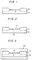
- FIG. 1 is a schematic cross-sectional view showing the manner in which a field oxide film is formed on a silicon substrate in a first embodiment of this invention;
- FIG. 2 is a schematic cross-sectional view showing the manner in which a RCA cleaning is performed to form a chemical oxide film in the first embodiment;
- FIG. 3 is a schematic cross-sectional view showing the manner in which the substrate of FIG. 2 is cleansed by wet etching in the first embodiment;
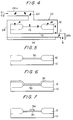
- FIG. 4 is a schematic cross-sectional view showing the manner in which the substrate is further cleansed by dry etching in the first embodiment;
- FIG. 5 is a schematic cross-sectional view showing the manner in which a gate oxide film is formed in the first embodiment;
- FIG. 6 is a schematic cross-sectional view showing the manner in which a polycrystalline silicon layer is formed in the first embodiment;
- FIG. 7 is a schematic cross-sectional view showing the manner in which a gate electrode is formed in the first embodiment;
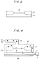
- FIG. 8 is a schematic cross-sectional view showing the manner in which a field oxide film is formed in a second embodiment of the invention; and
- FIG. 9 is a schematic cross-sectional view showing the manner in which cleansing is accomplished by dry etching.
- FIGS. 1 through 7 show a series of manufacturing steps according to the first embodiment of this invention.
- In this embodiment, an n-channel MOSFET is manufactured by the way of illustrative example.
- (a) In the step shown in FIG. 1, a
field oxide film 12 is formed on a p-type silicon substrate 10 in the usual method. Before advancing to the next step, anatural oxide film 18, which is formed on thesilicon substrate 10, is removed by wet etching with an HF cleaning solution. - (b) In the step shown in FIG. 2, the surface of the
silicon substrate 10 is cleansed by a so-called RCA cleaning, which is accomplished by an oxide agent containing NH₄OH-H₂O₂, HCl-H₂O₂.
At that time, in achemical oxide film 14 formed by the RCA cleaning,metal impurities 16 such as aluminum, iron, copper, zinc, chrome or nickel exist chiefly due to the stay of metal in the ingredients of the RCA cleaning solution. Of these metals, aluminum and iron are most popular. So, it is important to remove these metals. - (c) In the step shown in FIG. 3, in order to remove the contaminated substances such as the residuals of the RCA cleaning solution and the metal impurities in the
chemical oxide film 14, wet cleaning is performed in awet etching unit 20. An etching solution to be used in this step contains preferably nitric acid and HF, for example. After the wet cleaning, the usual rinsing and drying are performed. By this step, most of thechemical oxide film 14 and the contaminated substances are removed. - (d) In the step shown in FIG. 4, the wet-cleaned substrate is dry-cleaned by a
dry etching unit 22. As a significant feature of this step, a chlorine gas G2 together with an HF etching gas G1 is supplied into achamber 24 via an inlet 28a. The interior of thechamber 24 is heated by aheater 26 and is decompressed to a pressure lower than the normal atmospheric pressure.
This dry etching is performed under the following conditions:
Pressure in the chamber 24: 0.1 to 0.5 Torr.
Temperature in the chamber 24: 10 to 100°C
Flow of HF gas: 50 to 100 SCC/minute
Flow of chlorine gas: 0.1 to 0.5 SCC/minute
These conditions may be set otherwise within the appropriate scopes, depending on the presence/absence of wet cleaning, the state of the substrate, the thickness of an oxide film, the kind of the oxide film, etc.
In this step, the particles and metal impurities on the substrate are removed almost perfectly, obtaining a contamination-free clean substrate surface. In other words, the chlorine gas G2 reacts with themetal impurities 16 existing on the surface of thesubstrate 10 and thefield oxide film 12, forming a metal chloride C. Since generally this metal chloride C is apt to be vaporized, the metal chloride C is released into the space in thechamber 24 under decompressure or under high heat and decompression and is then discharged to the outside from anoutlet 28b. By dry etching with the HF gas G1, thechemical oxide film 14 is etched with the particles removed almost perfectly from the surface of thesubstrate 10. - (e) In the step shown in FIG. 5, in a clean room, thermal oxidation is performed to form a
gate oxide film 30 having a thickness of tens to hundreds Angstrom. - (f) In the step shown in FIG. 6, a p-type impurity, such as boron, constituting a channel is doped in the usual method, whereupon a
polycrystalline silicon layer 32 is formed. - (g) In the step shown in FIG. 7, an n-type impurity such as phosphorous is doped in the usual method, whereupon a
gate electrode 30 is formed by the usual photolithography and etching technology. - Further, although there is no illustration in the drawings, a source diffused region and a drain diffused region are formed by doping an n-type impurity such as arsenic in the usual method, and metallization is performed to form an electrode.
- In this embodiment, the substance containing a chlorine atom was a chlorine gas for the most suitable example. However, it should by no means be limited to this specific example and may be an HCl gas, for example.
- FIGS. 8 and 9 shows a series of manufacturing steps according to the second embodiment of this invention.
- In this embodiment, the
silicon substrate 10 with afield oxide film 12 formed thereon (corresponding to the step (a)) is dry-cleaned directly by etching by adry etching unit 22, omitting the RCA-cleaning step (step (b)) and the wet etching step (step (c)). Since the dry etching step shown in FIG. 9 is basically identical with the dry etching stop (the above-mentioned step (d)), its detailed description is omitted here for clarity. - In this embodiment, since the RCA-cleaning step and the wet etching step are omitted, dry cleaning in the dry etching step should be performed more adequately, compared to the first embodiment.
- Although certain preferred embodiments have been shown and described, it should be understood that many changes and modifications may be made therein without departing from the scope of the appended claims. For example, the wet etching step (step (c)) may be omitted in the first embodiment. In the cleansing step of this invention, a conventional alternative mean may be added at a necessary stage. Further, this invention is also applicable to the production of an p-type MOSFET as well as a n-type MOSFET.
Claims (7)
- A method of manufacturing a semiconductor device including a MOS-type field effect transistor, comprising the steps of:(a) cleansing a surface of a substrate;(b) forming, next to said cleansing, a gate oxide film on the cleansed surface of the substrate;(c) dry-etching, during said cleansing step, the surface of the substrate in an ambient in which hydrogen fluoride and a substance containing at least a chloride atom coexist in a gaseous state; and(d) removing, during said cleansing step, an oxide film and metal impurities on the surface of the substrate.
- A method according to claim 1, wherein said dry-etching is performed under heat and decompression.
- A method according to claim 1, wherein said substance containing at least a chlorine atom is one selected from the group consisting of chlorine and hydrochloric acid.
- A method according to claim 1, wherein during said cleansing step, RCA cleaning is performed before said dry-etching.
- A method according to claim 1, wherein during said cleansing step, wet-etching is performed before said dry-etching.
- A method according to claim 5, wherein said wet-etching is accomplished by using a cleaning solution containing nitric acid and hydrogen fluoride.
- A method according to claim 1, wherein during said cleansing step, RCA cleaning and wet etching are performed before said dry-etching.
Applications Claiming Priority (2)
| Application Number | Priority Date | Filing Date | Title |
|---|---|---|---|
| JP321750/90 | 1990-11-26 | ||
| JP32175090 | 1990-11-26 |
Publications (2)
| Publication Number | Publication Date |
|---|---|
| EP0488148A2 true EP0488148A2 (en) | 1992-06-03 |
| EP0488148A3 EP0488148A3 (en) | 1992-08-12 |
Family
ID=18136031
Family Applications (1)
| Application Number | Title | Priority Date | Filing Date |
|---|---|---|---|
| EP19910120153 Withdrawn EP0488148A3 (en) | 1990-11-26 | 1991-11-26 | Method of manufacturing a mos-type field-effect transistor |
Country Status (4)
| Country | Link |
|---|---|
| US (1) | US5238871A (en) |
| EP (1) | EP0488148A3 (en) |
| JP (1) | JPH0521459A (en) |
| KR (1) | KR920010774A (en) |
Cited By (3)
| Publication number | Priority date | Publication date | Assignee | Title |
|---|---|---|---|---|
| DE19510922A1 (en) * | 1994-03-25 | 1995-09-28 | Mitsubishi Electric Corp | Method for producing a semiconductor component, method for cleaning a crystal surface of a semiconductor and semiconductor component |
| EP0692819A3 (en) * | 1994-07-07 | 1997-07-02 | Toshiba Kk | Method of manufacturing a semiconductor device including pre-oxidation process |
| EP0964439A1 (en) * | 1998-06-09 | 1999-12-15 | Air Products And Chemicals, Inc. | Gas phase removal of SIO2/metallic contaminants from silicon |
Families Citing this family (8)
| Publication number | Priority date | Publication date | Assignee | Title |
|---|---|---|---|---|
| US5589422A (en) * | 1993-01-15 | 1996-12-31 | Intel Corporation | Controlled, gas phase process for removal of trace metal contamination and for removal of a semiconductor layer |
| US5966623A (en) * | 1995-10-25 | 1999-10-12 | Eastman Kodak Company | Metal impurity neutralization within semiconductors by fluorination |
| JP3676912B2 (en) * | 1997-08-07 | 2005-07-27 | 株式会社ルネサステクノロジ | Semiconductor manufacturing apparatus and foreign matter removing method thereof |
| US5980770A (en) * | 1998-04-16 | 1999-11-09 | Siemens Aktiengesellschaft | Removal of post-RIE polymer on Al/Cu metal line |
| US6715497B2 (en) * | 2001-01-02 | 2004-04-06 | International Business Machines Corporation | Treatment to eliminate polysilicon defects induced by metallic contaminants |
| US20020176984A1 (en) * | 2001-03-26 | 2002-11-28 | Wilson Smart | Silicon penetration device with increased fracture toughness and method of fabrication |
| JP2005275231A (en) * | 2004-03-26 | 2005-10-06 | Fuji Photo Film Co Ltd | Photosensitive lithographic printing plate |
| US20070048991A1 (en) * | 2005-08-23 | 2007-03-01 | Taiwan Semiconductor Manufacturing Co., Ltd. | Copper interconnect structures and fabrication method thereof |
Citations (2)
| Publication number | Priority date | Publication date | Assignee | Title |
|---|---|---|---|---|
| US4264374A (en) * | 1978-09-25 | 1981-04-28 | International Business Machines Corporation | Cleaning process for p-type silicon surface |
| US4923828A (en) * | 1989-07-07 | 1990-05-08 | Eastman Kodak Company | Gaseous cleaning method for silicon devices |
Family Cites Families (2)
| Publication number | Priority date | Publication date | Assignee | Title |
|---|---|---|---|---|
| US3426422A (en) * | 1965-10-23 | 1969-02-11 | Fairchild Camera Instr Co | Method of making stable semiconductor devices |
| JPH01204427A (en) * | 1988-02-10 | 1989-08-17 | Hitachi Ltd | Semiconductor device |
-
1991
- 1991-11-25 US US07/796,825 patent/US5238871A/en not_active Expired - Fee Related
- 1991-11-25 KR KR1019910021221A patent/KR920010774A/en not_active Application Discontinuation
- 1991-11-25 JP JP3309205A patent/JPH0521459A/en active Pending
- 1991-11-26 EP EP19910120153 patent/EP0488148A3/en not_active Withdrawn
Patent Citations (2)
| Publication number | Priority date | Publication date | Assignee | Title |
|---|---|---|---|---|
| US4264374A (en) * | 1978-09-25 | 1981-04-28 | International Business Machines Corporation | Cleaning process for p-type silicon surface |
| US4923828A (en) * | 1989-07-07 | 1990-05-08 | Eastman Kodak Company | Gaseous cleaning method for silicon devices |
Non-Patent Citations (2)
| Title |
|---|
| EXTENDED ABSTRACTS. vol. 88-1, 15 May 1988, PRINCETON, NEW JERSEY US pages 161 - 162; D. FRYSTAK ET AL.: 'Remote plasma removal of metallic impurities from silicon surfaces.' * |
| JAPANESE JOURNAL OF APPLIED PHYSICS, EXTENDED ABSTRACTS OF THE 22ND (1990) CONFERENCE ON SOLID STATE DEVICES AND MATERIALS, TOKYO JA pages 1103 - 1106; Y. SATO ET AL.: 'Reliability-Improvement of the MOS Structures Photo-Excited Dry Cleaning before Oxidation.' * |
Cited By (7)
| Publication number | Priority date | Publication date | Assignee | Title |
|---|---|---|---|---|
| DE19510922A1 (en) * | 1994-03-25 | 1995-09-28 | Mitsubishi Electric Corp | Method for producing a semiconductor component, method for cleaning a crystal surface of a semiconductor and semiconductor component |
| GB2288067A (en) * | 1994-03-25 | 1995-10-04 | Mitsubishi Electric Corp | Removing oxide films during semiconductor device fabrication |
| GB2288067B (en) * | 1994-03-25 | 1997-11-12 | Mitsubishi Electric Corp | Method of fabricating a semiconductor device,method of cleaning a crystalline surface of a semiconductor,and semiconductor device |
| US5948161A (en) * | 1994-03-25 | 1999-09-07 | Mitsubishi Denki Kabushiki Kaisha | Method of fabricating a semiconductor device and method of cleaning a crystalline semiconductor surface |
| EP0692819A3 (en) * | 1994-07-07 | 1997-07-02 | Toshiba Kk | Method of manufacturing a semiconductor device including pre-oxidation process |
| US5731247A (en) * | 1994-07-07 | 1998-03-24 | Kabushiki Kaisha Toshiba | Method for manufacturing a semiconductor device including pre-oxidation process |
| EP0964439A1 (en) * | 1998-06-09 | 1999-12-15 | Air Products And Chemicals, Inc. | Gas phase removal of SIO2/metallic contaminants from silicon |
Also Published As
| Publication number | Publication date |
|---|---|
| JPH0521459A (en) | 1993-01-29 |
| EP0488148A3 (en) | 1992-08-12 |
| US5238871A (en) | 1993-08-24 |
| KR920010774A (en) | 1992-06-27 |
Similar Documents
| Publication | Publication Date | Title |
|---|---|---|
| US4808259A (en) | Plasma etching process for MOS circuit pregate etching utiliizing a multi-step power reduction recipe | |
| US5238871A (en) | Method of manufacturing a semiconductor device | |
| KR100933247B1 (en) | Substrate processing apparatus, substrate processing method, and manufacturing method of semiconductor device | |
| US5599735A (en) | Method for doped shallow junction formation using direct gas-phase doping | |
| US6235590B1 (en) | Fabrication of differential gate oxide thicknesses on a single integrated circuit chip | |
| JP2520990B2 (en) | Method for manufacturing low defect polysilicon integrated circuit | |
| US5492854A (en) | Method of manufacturing semiconductor device | |
| KR100399492B1 (en) | Semiconductor device having wiring or electrode on silicon layer and method of forming the wiring or electrode | |
| US5928786A (en) | Monocrystalline silicon wafer and method of thermally oxidizing a surface thereof | |
| JP4240637B2 (en) | Wafer surface cleaning method | |
| JP3686163B2 (en) | Manufacturing method of semiconductor integrated circuit device and manufacturing apparatus thereof | |
| TW442897B (en) | Process for modified oxidation of a semiconductor substrate using chlorine plasma | |
| JP3272823B2 (en) | Dry cleaning method for semiconductor device | |
| JPH05144802A (en) | Cleaning method for semiconductor manufacturing device | |
| US6908793B2 (en) | Method for fabricating a semiconductor device | |
| JP3716007B2 (en) | Manufacturing method of semiconductor device | |
| CN109003881B (en) | Formation of metal oxide layer | |
| JP2808933B2 (en) | Method for manufacturing semiconductor device | |
| JPH03173131A (en) | Manufacture of semiconductor device | |
| EP0331555A1 (en) | Gettering treatment process | |
| US7148132B2 (en) | Manufacturing method of semiconductor device | |
| EP0989604A2 (en) | In situ deposition of gate oxide and amorphous silicon electrode and corresponding structure | |
| JPH08107205A (en) | Manufacture of sacrificial oxide film | |
| JPH0645593A (en) | Manufacture of transistor | |
| KR0170351B1 (en) | Cleaning solution manufacturing method and cleaning method using the same |
Legal Events
| Date | Code | Title | Description |
|---|---|---|---|
| PUAI | Public reference made under article 153(3) epc to a published international application that has entered the european phase |
Free format text: ORIGINAL CODE: 0009012 |
|
| AK | Designated contracting states |
Kind code of ref document: A2 Designated state(s): DE FR GB NL |
|
| PUAL | Search report despatched |
Free format text: ORIGINAL CODE: 0009013 |
|
| AK | Designated contracting states |
Kind code of ref document: A3 Designated state(s): DE FR GB NL |
|
| 17P | Request for examination filed |
Effective date: 19930119 |
|
| 17Q | First examination report despatched |
Effective date: 19941014 |
|
| STAA | Information on the status of an ep patent application or granted ep patent |
Free format text: STATUS: THE APPLICATION IS DEEMED TO BE WITHDRAWN |
|
| 18D | Application deemed to be withdrawn |
Effective date: 19950425 |