EP0488554A2 - Tab tape, tab tape package and method of bonding same - Google Patents
Tab tape, tab tape package and method of bonding same Download PDFInfo
- Publication number
- EP0488554A2 EP0488554A2 EP91310540A EP91310540A EP0488554A2 EP 0488554 A2 EP0488554 A2 EP 0488554A2 EP 91310540 A EP91310540 A EP 91310540A EP 91310540 A EP91310540 A EP 91310540A EP 0488554 A2 EP0488554 A2 EP 0488554A2
- Authority
- EP
- European Patent Office
- Prior art keywords
- chip
- tab tape
- pads
- opening
- leads
- Prior art date
- Legal status (The legal status is an assumption and is not a legal conclusion. Google has not performed a legal analysis and makes no representation as to the accuracy of the status listed.)
- Withdrawn
Links
Images


Classifications
-
- H—ELECTRICITY
- H01—ELECTRIC ELEMENTS
- H01L—SEMICONDUCTOR DEVICES NOT COVERED BY CLASS H10
- H01L23/00—Details of semiconductor or other solid state devices
- H01L23/48—Arrangements for conducting electric current to or from the solid state body in operation, e.g. leads, terminal arrangements ; Selection of materials therefor
- H01L23/488—Arrangements for conducting electric current to or from the solid state body in operation, e.g. leads, terminal arrangements ; Selection of materials therefor consisting of soldered or bonded constructions
- H01L23/495—Lead-frames or other flat leads
- H01L23/49572—Lead-frames or other flat leads consisting of thin flexible metallic tape with or without a film carrier
-
- H—ELECTRICITY
- H01—ELECTRIC ELEMENTS
- H01L—SEMICONDUCTOR DEVICES NOT COVERED BY CLASS H10
- H01L24/00—Arrangements for connecting or disconnecting semiconductor or solid-state bodies; Methods or apparatus related thereto
- H01L24/01—Means for bonding being attached to, or being formed on, the surface to be connected, e.g. chip-to-package, die-attach, "first-level" interconnects; Manufacturing methods related thereto
- H01L24/50—Tape automated bonding [TAB] connectors, i.e. film carriers; Manufacturing methods related thereto
-
- H—ELECTRICITY
- H01—ELECTRIC ELEMENTS
- H01L—SEMICONDUCTOR DEVICES NOT COVERED BY CLASS H10
- H01L24/00—Arrangements for connecting or disconnecting semiconductor or solid-state bodies; Methods or apparatus related thereto
- H01L24/80—Methods for connecting semiconductor or other solid state bodies using means for bonding being attached to, or being formed on, the surface to be connected
- H01L24/86—Methods for connecting semiconductor or other solid state bodies using means for bonding being attached to, or being formed on, the surface to be connected using tape automated bonding [TAB]
-
- H—ELECTRICITY
- H01—ELECTRIC ELEMENTS
- H01L—SEMICONDUCTOR DEVICES NOT COVERED BY CLASS H10
- H01L2224/00—Indexing scheme for arrangements for connecting or disconnecting semiconductor or solid-state bodies and methods related thereto as covered by H01L24/00
- H01L2224/01—Means for bonding being attached to, or being formed on, the surface to be connected, e.g. chip-to-package, die-attach, "first-level" interconnects; Manufacturing methods related thereto
- H01L2224/10—Bump connectors; Manufacturing methods related thereto
- H01L2224/15—Structure, shape, material or disposition of the bump connectors after the connecting process
- H01L2224/16—Structure, shape, material or disposition of the bump connectors after the connecting process of an individual bump connector
-
- H—ELECTRICITY
- H01—ELECTRIC ELEMENTS
- H01L—SEMICONDUCTOR DEVICES NOT COVERED BY CLASS H10
- H01L24/00—Arrangements for connecting or disconnecting semiconductor or solid-state bodies; Methods or apparatus related thereto
- H01L24/74—Apparatus for manufacturing arrangements for connecting or disconnecting semiconductor or solid-state bodies
- H01L24/79—Apparatus for Tape Automated Bonding [TAB]
-
- H—ELECTRICITY
- H01—ELECTRIC ELEMENTS
- H01L—SEMICONDUCTOR DEVICES NOT COVERED BY CLASS H10
- H01L2924/00—Indexing scheme for arrangements or methods for connecting or disconnecting semiconductor or solid-state bodies as covered by H01L24/00
- H01L2924/01—Chemical elements
- H01L2924/01005—Boron [B]
-
- H—ELECTRICITY
- H01—ELECTRIC ELEMENTS
- H01L—SEMICONDUCTOR DEVICES NOT COVERED BY CLASS H10
- H01L2924/00—Indexing scheme for arrangements or methods for connecting or disconnecting semiconductor or solid-state bodies as covered by H01L24/00
- H01L2924/01—Chemical elements
- H01L2924/01029—Copper [Cu]
-
- H—ELECTRICITY
- H01—ELECTRIC ELEMENTS
- H01L—SEMICONDUCTOR DEVICES NOT COVERED BY CLASS H10
- H01L2924/00—Indexing scheme for arrangements or methods for connecting or disconnecting semiconductor or solid-state bodies as covered by H01L24/00
- H01L2924/01—Chemical elements
- H01L2924/01033—Arsenic [As]
-
- H—ELECTRICITY
- H01—ELECTRIC ELEMENTS
- H01L—SEMICONDUCTOR DEVICES NOT COVERED BY CLASS H10
- H01L2924/00—Indexing scheme for arrangements or methods for connecting or disconnecting semiconductor or solid-state bodies as covered by H01L24/00
- H01L2924/01—Chemical elements
- H01L2924/01079—Gold [Au]
-
- H—ELECTRICITY
- H01—ELECTRIC ELEMENTS
- H01L—SEMICONDUCTOR DEVICES NOT COVERED BY CLASS H10
- H01L2924/00—Indexing scheme for arrangements or methods for connecting or disconnecting semiconductor or solid-state bodies as covered by H01L24/00
- H01L2924/01—Chemical elements
- H01L2924/01082—Lead [Pb]
-
- H—ELECTRICITY
- H01—ELECTRIC ELEMENTS
- H01L—SEMICONDUCTOR DEVICES NOT COVERED BY CLASS H10
- H01L2924/00—Indexing scheme for arrangements or methods for connecting or disconnecting semiconductor or solid-state bodies as covered by H01L24/00
- H01L2924/10—Details of semiconductor or other solid state devices to be connected
- H01L2924/11—Device type
- H01L2924/14—Integrated circuits
-
- Y—GENERAL TAGGING OF NEW TECHNOLOGICAL DEVELOPMENTS; GENERAL TAGGING OF CROSS-SECTIONAL TECHNOLOGIES SPANNING OVER SEVERAL SECTIONS OF THE IPC; TECHNICAL SUBJECTS COVERED BY FORMER USPC CROSS-REFERENCE ART COLLECTIONS [XRACs] AND DIGESTS
- Y10—TECHNICAL SUBJECTS COVERED BY FORMER USPC
- Y10T—TECHNICAL SUBJECTS COVERED BY FORMER US CLASSIFICATION
- Y10T29/00—Metal working
- Y10T29/49—Method of mechanical manufacture
- Y10T29/49002—Electrical device making
- Y10T29/49117—Conductor or circuit manufacturing
- Y10T29/49121—Beam lead frame or beam lead device
-
- Y—GENERAL TAGGING OF NEW TECHNOLOGICAL DEVELOPMENTS; GENERAL TAGGING OF CROSS-SECTIONAL TECHNOLOGIES SPANNING OVER SEVERAL SECTIONS OF THE IPC; TECHNICAL SUBJECTS COVERED BY FORMER USPC CROSS-REFERENCE ART COLLECTIONS [XRACs] AND DIGESTS
- Y10—TECHNICAL SUBJECTS COVERED BY FORMER USPC
- Y10T—TECHNICAL SUBJECTS COVERED BY FORMER US CLASSIFICATION
- Y10T29/00—Metal working
- Y10T29/49—Method of mechanical manufacture
- Y10T29/49002—Electrical device making
- Y10T29/49117—Conductor or circuit manufacturing
- Y10T29/49124—On flat or curved insulated base, e.g., printed circuit, etc.
- Y10T29/4913—Assembling to base an electrical component, e.g., capacitor, etc.
- Y10T29/49144—Assembling to base an electrical component, e.g., capacitor, etc. by metal fusion
Definitions
- This invention relates to TAB (Tape Automated Bonding) tape techniques, and more specifically to TAB tapes, TAB tape packages and methods of bonding the same.
- TAB Transmission Automated Bonding
- TAB tape is widely used in manufacturing semiconductor integrated circuit packages.
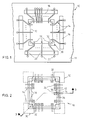
- a conventional TAB tape 10, Figures 6 and 7 comprises an insulating tape 11 of a material such as polyimide, through which tape there is a multiplicity of openings 12, each shaped to receive a semiconductor chip 24.
- the insulating tape 11 has an opening 12 at each chip attaching position and leads 14 are formed on the tape 11 around each opening 12.
- Four elongated slots 16 are formed on the tape 11 around each opening 12.
- Each lead 14 has an inner lead portion 18 projecting into opening 12 and an outer lead portion 20 extending across slot 16.
- the outer lead portions 20 terminate in test pads 22 which are used for circuitry testing.
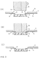
- a semiconductor chip When a chip is to be attached to a TAB tape, a semiconductor chip is positioned in opening 12, and inner lead portions 18 are connected to the pads of the chip by the use of a bonding tool 28 (Figure 8) called Thermode.
- the tape 10 is placed so that leads 14 face downward ( Figure 8 (A)), and tape 11 and chip 24 are so positioned that inner lead portions 18 and electrode pads 26 of the chip 24 are aligned with each other. All the inner lead portions 18 are thermocompressively bonded simultaneously to chip pads 26 by means of the bonding tool 28.
- the top end of the bonding tool 28 is formed of a hard material such as a sintered diamond, and the leads 14, are usually formed of copper, plated with tin.
- This bonding method is satisfactory when the number of leads is small, but a problem of lift-up of chips occurs as the number of leads is increased.
- the bonding tool is raised after the bonding, it may happen that chip 24 ( Figure 8 (B)) is lifted up at the same time, making the leads deform, whereby the inner lead portions 18 are brought in contact with the edge of chip 24.
- a surface of a chip is usually covered with a surface protecting layer such as polyimide, it is not always completely covered to its edge portion.
- a surface protecting layer such as polyimide
- this invention seeks to provide a TAB tape, package and bonding method for preventing a chip from being lifted up by adhesion of the bonding tool with the leads in the bonding of the TAB leads.
- This invention also seeks to provide a TAB package which can prevent contact between the leads and the chip.
- the invention provides a TAB tape which includes insulating tape having openings at respective chip attaching positions, and leads formed on the insulating tape and extending into respective openings to be connected to pads of the respective chips when the chips are attached, characterised by chip pressure means on the insulating tape extending into each opening to prevent passage of a chip therethrough.
- the attachment of the chips is by a bonding tool pressing the lead extensions against the chip pads, and the chip pressure means extends into each opening to prevent a chip from being lifted up by adhesion between the bonding tool and the leads when the chip is attached.
- the invention extends to a TAB tape package comprising such a TAB tape, in which the leads have inner lead portions extending into the opening and outer lead portions extending from the insulating tape, a chip is disposed in the opening and has pads connected to the inner lead portions, and the chip pressure means extends into the opening to prevent contact between the inner lead portion and the chip by engagement with the surface of the chip at the side of the pad.
- the invention includes a method of bonding a TAB tape, comprising preparing such a tape, aligning the tape with respect to a chip so that the lead portions in a selected opening are positioned on the pads of the chip to be attached and projecting portions of the chip pressure means in the opening are positioned on the surface at the side of the pads, moving a bonding tool downwardly to the selected opening, the bonding tool having a bottom surface for thermocompressively bonding the lead portions to the pads and inclined surfaces for engaging the projecting portions and bending the projecting portions towards the surface at the side of the pads by engagement of the inclined surfaces with the projecting portions during the downward movement of said bonding tool.
- the TAB tape is so formed as to have chip pressure means extending into the openings in which chips are to be attached.
- the chip pressure means are preferably formed of the same material as the leads and provided at the same side as the leads and in the four corners of the openings in which the chips are to be attached.
- the chip pressure means act to engage with the surface of a chip at the side of the pads thereby preventing the chip from lifting or moving to the leads.
- a TAB tape 10 ( Figure 1) includes a length of insulating tape 11 of polyimide, which is 125 microns thick. A multiplicity of openings 12 are formed through the tape 11 in the positions in which chips are to be attached. A total of two hundred and sixty-eight leads 14 is provided for each opening 12 and these are formed on the tape 11 of 35 micron-thick copper having a tin surface coating. Detailed structures such as sprocket holes are omitted in the figure.
- each chip pressure member 30 is provided in each of the four corners of each opening 12 ( Figure 1).
- a portion 32 of each chip pressure member 30 extends into opening 12.
- Leads 14 are usually formed by patterning a copper layer bonded to the polyimide tape.
- the chip pressure members 30 are preferably formed on the same side of the tape 11 and of the same material as leads 14, conveniently by patterning the copper layer so as simultaneously to form leads 14 and chip pressure members 30.
- the tape 10 ( Figure 2) and chip 24 are aligned so that inner lead portions 18 and electrode pads 26 of semiconductor chip 24 align with each other at the time of bonding.
- the tape is placed so that the leads face downward.
- Projecting portions 32 of chip pressure members 30 overhang the four corners of chip 24 so as to be capable of engaging with the surface of chip 24 at the side of pads 26.
- the chip pressure member portions 32 extend to such an extent as to overlap slightly the bottom of the bonding tool 28, whose shape is represented by the broken line 34.
- the shape 34 of the bottom of the tool 28 is such that, during bonding ( Figure 3) the bottom contacts with all the inner lead portions 18.
- the corners of the bottom are cut away to form inclined surfaces 36 so as not to engage the main part of the projecting portions 32 of chip pressure members 30, but only the extremities.
- the inclined surfaces 36 are provided in the corners of the bottom surface 34 of the bonding tool 28 corresponding to the chip pressure members 30.
- the projecting portions 32 of the chip pressure members 30 engage with the upper surface of the chip at the side of the pads to block further movement, and thus lifting-up of the chip and hence the deformation of the leads can be prevented.
- the projecting portions 32 which were bent act as spacers to maintain the spacing between the chip surface and the lead portions 18.
- a difference needs to occur between the height of the chip pressure members 30 and that of the bottom surface of the tool in its lowest position. If gold is used as the material for chip pads 26, the thickness of the gold pads is ordinarily reduced by a factor of several numbers. Thus, the design needs to be made such that the necessary difference in height is obtained, considering the thickness change.
- chip pressure member 30 Two alternative forms of chip pressure member 30 are shown in Figure 4.
- the projecting portion has two protrusions 38.
- the projecting portion 32 is substantially rectangular. It will be apparent that the shape of the chip pressure members 30 is not limited to these forms, but they can be formed to any suitable shape.
- the chip pressure members may be formed on the surface of the insulating tape which is opposite to that on which the leads are formed.
- the chip pressure members in the four corners need not always be separated.
- the chip pressure members need not always be provided in the four corners of a chip if the lead density is relatively small and if space for engagement of the chip pressure members can be secured in positions other than the four corners.
- the chip pressure members need not be of the same material as the leads.
- the TAB tape was bonded with the leads facing downward, it may be bonded with the leads facing upward.
- a chip can easily and securely be prevented from being lifted up by the adhesion between the bonding tool and the leads at the time of bonding.
- a TAB package structure can be obtained wherein the spacing between the leads and the chip surface can be maintained and thus the contact of the leads with the chip can be prevented even after the bonding.
- the chip pressure members are so called because, if the chip starts to lift lip by reason of adhesion between the bonding tool and the leads thermocompressively bonded to the chip pads, the chip pressure members engage the chip and prevent such lift-up, pressing against the chip as the bonding tool rises.
- the tips of the chip pressure members should be engaged by the inclined surfaces of the corners of the bottom of the tool and bent into contact with the surface of the chip, but no further. Such an arrangement ensures that the leads are not damaged by lift-up of the chip.
- the chip pressure members may be formed simultaneously with the leads on the insulating tape by appropriate etching of a metallisation layer on the tape.
Abstract
A TAB tape 10 comprises an insulating tape having a multiplicity of openings 12, each surrounded by metallic leads 14 having inner lead portions 18 projecting into the opening 12. In the corners of the opening 12 on the tape are formed metallic chip pressure members 30 having tips 32 projecting into the opening 12 between groups of inner lead portions 18. A chip 24 is positioned in each opening 12 in turn with chip pads 26 aligned with the inner lead portions 18. A bonding tool 34 is moved downwardly into engagement with the inner lead portions 18 to force them into contact with the chip pads 26 and to thermocompressively attach them thereto. The corners of the tool 34 engage and bend the tips 32 into engagement with the surface of the chip 24, so that when the tool is lifted, the chip is prevented from following due to adhesion of the tool and leads.
Description
- This invention relates to TAB (Tape Automated Bonding) tape techniques, and more specifically to TAB tapes, TAB tape packages and methods of bonding the same.
- TAB tape is widely used in manufacturing semiconductor integrated circuit packages. A
conventional TAB tape 10, Figures 6 and 7 comprises aninsulating tape 11 of a material such as polyimide, through which tape there is a multiplicity ofopenings 12, each shaped to receive asemiconductor chip 24. Theinsulating tape 11 has an opening 12 at each chip attaching position andleads 14 are formed on thetape 11 around each opening 12. Fourelongated slots 16 are formed on thetape 11 around each opening 12. Eachlead 14 has aninner lead portion 18 projecting into opening 12 and anouter lead portion 20 extending acrossslot 16. Theouter lead portions 20 terminate intest pads 22 which are used for circuitry testing. - When a chip is to be attached to a TAB tape, a semiconductor chip is positioned in opening 12, and
inner lead portions 18 are connected to the pads of the chip by the use of a bonding tool 28 (Figure 8) called Thermode. Thetape 10 is placed so that leads 14 face downward (Figure 8 (A)), andtape 11 andchip 24 are so positioned thatinner lead portions 18 andelectrode pads 26 of thechip 24 are aligned with each other. All theinner lead portions 18 are thermocompressively bonded simultaneously tochip pads 26 by means of thebonding tool 28. - The top end of the
bonding tool 28 is formed of a hard material such as a sintered diamond, and theleads 14, are usually formed of copper, plated with tin. This bonding method is satisfactory when the number of leads is small, but a problem of lift-up of chips occurs as the number of leads is increased. When the number of leads increases, the contact area between the bonding tool and leads increases and the adhesive force between the bonding tool and leads increases. For this reason, when the bonding tool is raised after the bonding, it may happen that chip 24 (Figure 8 (B)) is lifted up at the same time, making the leads deform, whereby theinner lead portions 18 are brought in contact with the edge ofchip 24. - Although the surface of a chip is usually covered with a surface protecting layer such as polyimide, it is not always completely covered to its edge portion. In addition, there are chips of the type in which an exposed wiring pattern for evaluating the chip characteristics is provided in the edge portion. Accordingly, it is not desirable for the leads to touch the chip.
- The above problem can be solved by adding a work step to restore the deformed leads, but such work is inefficient and also may damage the leads or chip. Another method can be imagined, in which a chip is sucked by vacuum and fixed that way at the time of bonding. However, this method would be complex and expensive because it requires a vacuum control mechanism, and it also requires extra control time. Although forming the bonding tool and leads with materials which do not adhere to each other can be considered as a further method, no practical technique for this has been proposed.
- It is preferable to ensure the prevention of contact between the leads and the chip even after the bonding. This is not ensured by the above-mentioned vacuum suction method.
- Accordingly, this invention seeks to provide a TAB tape, package and bonding method for preventing a chip from being lifted up by adhesion of the bonding tool with the leads in the bonding of the TAB leads.
- This invention also seeks to provide a TAB package which can prevent contact between the leads and the chip.
- From one aspect, the invention provides a TAB tape which includes insulating tape having openings at respective chip attaching positions, and leads formed on the insulating tape and extending into respective openings to be connected to pads of the respective chips when the chips are attached, characterised by chip pressure means on the insulating tape extending into each opening to prevent passage of a chip therethrough.
- Preferably, the attachment of the chips is by a bonding tool pressing the lead extensions against the chip pads, and the chip pressure means extends into each opening to prevent a chip from being lifted up by adhesion between the bonding tool and the leads when the chip is attached.
- The invention extends to a TAB tape package comprising such a TAB tape, in which the leads have inner lead portions extending into the opening and outer lead portions extending from the insulating tape, a chip is disposed in the opening and has pads connected to the inner lead portions, and the chip pressure means extends into the opening to prevent contact between the inner lead portion and the chip by engagement with the surface of the chip at the side of the pad.
- The invention includes a method of bonding a TAB tape, comprising preparing such a tape, aligning the tape with respect to a chip so that the lead portions in a selected opening are positioned on the pads of the chip to be attached and projecting portions of the chip pressure means in the opening are positioned on the surface at the side of the pads, moving a bonding tool downwardly to the selected opening, the bonding tool having a bottom surface for thermocompressively bonding the lead portions to the pads and inclined surfaces for engaging the projecting portions and bending the projecting portions towards the surface at the side of the pads by engagement of the inclined surfaces with the projecting portions during the downward movement of said bonding tool.
- In an embodiment of TAB tape, to solve the problems the TAB tape is so formed as to have chip pressure means extending into the openings in which chips are to be attached. The chip pressure means are preferably formed of the same material as the leads and provided at the same side as the leads and in the four corners of the openings in which the chips are to be attached. The chip pressure means act to engage with the surface of a chip at the side of the pads thereby preventing the chip from lifting or moving to the leads.
- How the invention can be carried into effect is hereinafter particularly described with reference to the accompanying drawings, in which:
- Figure 1 is a schematic representation of part of a TAB tape according to this invention;
- Figure 2 is a schematic representation of part of the tape of Figure 1 with a chip placed in an opening of the tape;
- Figure 3 is a schematic sectional representation illustrating the bonding operation on the lines 3-3 of Figure 2;
- Figure 4 is a representation showing other examples of chip pressure member;
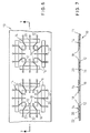
- Figure 5 is a schematic perspective representation of a TAB tape package according to this invention;
- Figure 6 is a schematic representation showing a conventional TAB tape;
- Figure 7 is a sectional view on line 7-7 of Figure 6; and Figure 8 is a representation showing conventional bonding operation.
- Corresponding elements in Figures 1 to 5 carry the same reference numerals as in Figures 6 to 8.
- In an exemplary embodiment of the invention, a TAB tape 10 (Figure 1) includes a length of
insulating tape 11 of polyimide, which is 125 microns thick. A multiplicity ofopenings 12 are formed through thetape 11 in the positions in which chips are to be attached. A total of two hundred and sixty-eightleads 14 is provided for eachopening 12 and these are formed on thetape 11 of 35 micron-thick copper having a tin surface coating. Detailed structures such as sprocket holes are omitted in the figure. - In each of the four corners of each opening 12 (Figure 1), a
chip pressure member 30 is provided. Aportion 32 of eachchip pressure member 30 extends into opening 12.Leads 14 are usually formed by patterning a copper layer bonded to the polyimide tape. Thechip pressure members 30 are preferably formed on the same side of thetape 11 and of the same material as leads 14, conveniently by patterning the copper layer so as simultaneously to formleads 14 andchip pressure members 30. - The tape 10 (Figure 2) and
chip 24 are aligned so thatinner lead portions 18 andelectrode pads 26 ofsemiconductor chip 24 align with each other at the time of bonding. In this example, the tape is placed so that the leads face downward. Projectingportions 32 ofchip pressure members 30 overhang the four corners ofchip 24 so as to be capable of engaging with the surface ofchip 24 at the side ofpads 26. - The chip
pressure member portions 32 extend to such an extent as to overlap slightly the bottom of thebonding tool 28, whose shape is represented by thebroken line 34. - The
shape 34 of the bottom of thetool 28 is such that, during bonding (Figure 3) the bottom contacts with all theinner lead portions 18. The corners of the bottom are cut away to forminclined surfaces 36 so as not to engage the main part of the projectingportions 32 ofchip pressure members 30, but only the extremities. Theinclined surfaces 36 are provided in the corners of thebottom surface 34 of thebonding tool 28 corresponding to thechip pressure members 30. - When the bonding tool 28 (Figure 3(A)) is lowered, the four
inclined surfaces 36 of the bonding tool are aligned with the projectingportions 32 ofchip pressure members 30. As the bonding tool moves further downwardly (Figure 3(B)), theinner lead portions 18 are engaged and depressed to thermocompressively bond them to pads 26. At the same time theinclined surfaces 36 engage the extremities or tips of the projectingportions 32 of thechip pressure members 30 and bend them down. When thebonding tool 28 rises after the bonding, thelead portions 18 may adhere to the bottom surface. If so and the chip lifts, the projectingportions 32 of thechip pressure members 30 engage with the upper surface of the chip at the side of the pads to block further movement, and thus lifting-up of the chip and hence the deformation of the leads can be prevented. The projectingportions 32 which were bent act as spacers to maintain the spacing between the chip surface and thelead portions 18. In order to bend the projectingportions 32 simultaneously with the bonding of the leads, a difference needs to occur between the height of thechip pressure members 30 and that of the bottom surface of the tool in its lowest position. If gold is used as the material forchip pads 26, the thickness of the gold pads is ordinarily reduced by a factor of several numbers. Thus, the design needs to be made such that the necessary difference in height is obtained, considering the thickness change. Even if the tip of the projectingportions 32 touches the chip surface, no problem occurs because the chip surface except for the pads is covered with a surface protecting insulating layer, a polyimide layer in this example, and the tip of the projectingportions 32 merely touch the polyimide layer. - Two alternative forms of
chip pressure member 30 are shown in Figure 4. In one, the projecting portion has twoprotrusions 38. In the other, the projectingportion 32 is substantially rectangular. It will be apparent that the shape of thechip pressure members 30 is not limited to these forms, but they can be formed to any suitable shape. - After bonding, the chip is tested using test pads 22 (Figure 1). By resin-sealing the surface of the chip at the side of the pads and then cutting along the outer edge of
slots 16 as needed, a single chip assembly is separated from the tape (Figure 5).Outer lead portions 20 are moulded into a shape suitable for being attached to a circuit board (not shown), whereby a TAB package is formed. - In addition to the above embodiments, various modifications are possible. For example, the chip pressure members may be formed on the surface of the insulating tape which is opposite to that on which the leads are formed. In this case, the chip pressure members in the four corners need not always be separated. Furthermore, the chip pressure members need not always be provided in the four corners of a chip if the lead density is relatively small and if space for engagement of the chip pressure members can be secured in positions other than the four corners. Moreover, if the spacing between the chip surface and the leads can be maintained after bonding, the chip pressure members need not be of the same material as the leads. In addition, although the TAB tape was bonded with the leads facing downward, it may be bonded with the leads facing upward.
- From the described embodiments of this invention, it will be appreciated that a chip can easily and securely be prevented from being lifted up by the adhesion between the bonding tool and the leads at the time of bonding. In addition, a TAB package structure can be obtained wherein the spacing between the leads and the chip surface can be maintained and thus the contact of the leads with the chip can be prevented even after the bonding.
- It will be appreciated that the chip pressure members are so called because, if the chip starts to lift lip by reason of adhesion between the bonding tool and the leads thermocompressively bonded to the chip pads, the chip pressure members engage the chip and prevent such lift-up, pressing against the chip as the bonding tool rises. For the preferred result, the tips of the chip pressure members should be engaged by the inclined surfaces of the corners of the bottom of the tool and bent into contact with the surface of the chip, but no further. Such an arrangement ensures that the leads are not damaged by lift-up of the chip. However, it will be appreciated that even if the chip pressure members are not contacted by the bottom of the tool, or are not bent into contact, the chip will engage the chip pressure members and be stopped if any lift-up occurs. This reduces the danger of damage to the leads.
It will also be appreciated that the chip pressure members may be formed simultaneously with the leads on the insulating tape by appropriate etching of a metallisation layer on the tape.
Claims (10)
- A TAB tape which includes insulating tape (11) having openings (12) at respective chip attaching positions, and leads (14) formed on the insulating tape (11) and extending (18) into respective openings (12) to be connected to pads (26) of the respective chips (24) when the chips are attached, characterised by chip pressure means (30) on the insulating tape (11) extending (32) into each opening (12) to prevent passage of a chip therethrough.
- A TAB tape according to claim 1, in which the attachment of the chips is by a bonding tool (28) pressing the lead extensions (18) against the chip pads (26), and the chip pressure means (30) extends (32) into each opening (12) to prevent a chip (24) from being lifted up by adhesion between the bonding tool (28) and the leads when the chip is attached.
- A TAB tape according to claim 1 or claim 2 wherein the chip pressure means (30) comprises metallic members formed on the insulating tape (11).
- A TAB tape according to claim 3, wherein the metallic members (30) are formed on the insulating tape (11) on the same side as the leads (14).
- A TAB tape according to claims 3 or 4, wherein the metallic members (30) are formed of the same material as the leads (14).
- A TAB tape according to any preceding claim, wherein the chip pressure means (30) extend into each opening (12) at the four corners thereof.
- A TAB tape according to any preceding claim, wherein the chip presure means (30) and the bonding tool (28) interengage during chip attachment so that the chip pressure means engages the surface of the chip to be attached away from the pads.
- A TAB tape package comprising a TAB tape according to any preceding claim, in which the leads (14) have inner lead portions (18) extending into the opening (12) and outer lead portions (20) extending from the insulating tape (11), a chip (24) is disposed in the opening and has pads (26) connected to the inner lead portions (18), and the chip pressure means (30) extends into the opening to prevent contact between the inner lead portion (18) and the chip (24) by engagement with the surface of the chip at the side of the pads (Figure 5).
- A TAB tape package according to claim 8, wherein the chip pressure means (30) has a projecting portion (32;38) bent towards the surface of the chip (24).
- A method of bonding a TAB tape, comprising preparing a TAB Tape according to any of claims 1 to 7, aligning the TAB tape with respect to a chip (24) so that the lead portions in a selected opening (12) are positioned on the pads (26) of the chip (24) to be attached and projecting portions (32) of the chip pressure means in the opening are positioned on the surface at the side of the pads, moving a bonding tool downwardly (28) to the selected opening, the bonding tool (28) having a bottom surface for thermocompressively bonding the lead portions (18) to the pads (26) and inclined surfaces (36) for engaging the projecting portions (32) and bending the projecting portions towards the surface at the side of the pads by engagement of the inclined surfaces with the projecting portions during the downward movement of said bonding tool.
Applications Claiming Priority (2)
| Application Number | Priority Date | Filing Date | Title |
|---|---|---|---|
| JP2323424A JPH088282B2 (en) | 1990-11-28 | 1990-11-28 | Method of joining TAB tape and semiconductor chip |
| JP323424/90 | 1990-11-28 |
Publications (2)
| Publication Number | Publication Date |
|---|---|
| EP0488554A2 true EP0488554A2 (en) | 1992-06-03 |
| EP0488554A3 EP0488554A3 (en) | 1993-06-02 |
Family
ID=18154534
Family Applications (1)
| Application Number | Title | Priority Date | Filing Date |
|---|---|---|---|
| EP19910310540 Withdrawn EP0488554A3 (en) | 1990-11-28 | 1991-11-14 | Tab tape, tab tape package and method of bonding same |
Country Status (3)
| Country | Link |
|---|---|
| US (2) | US5243141A (en) |
| EP (1) | EP0488554A3 (en) |
| JP (1) | JPH088282B2 (en) |
Cited By (2)
| Publication number | Priority date | Publication date | Assignee | Title |
|---|---|---|---|---|
| US5638596A (en) * | 1992-06-04 | 1997-06-17 | Lsi Logic Corporation | Method of employing multi-layer tab tape in semiconductor device assembly by selecting, breaking, downwardly bending and bonding tab tape trace free ends to a ground or power plane |
| US6124547A (en) * | 1997-02-17 | 2000-09-26 | Seiko Epson Corporation | Tape carrier package |
Families Citing this family (9)
| Publication number | Priority date | Publication date | Assignee | Title |
|---|---|---|---|---|
| JP2852178B2 (en) * | 1993-12-28 | 1999-01-27 | 日本電気株式会社 | Film carrier tape |
| US5477082A (en) * | 1994-01-11 | 1995-12-19 | Exponential Technology, Inc. | Bi-planar multi-chip module |
| US5938038A (en) | 1996-08-02 | 1999-08-17 | Dial Tool Industries, Inc. | Parts carrier strip and apparatus for assembling parts in such a strip |
| US5925926A (en) * | 1997-03-19 | 1999-07-20 | Nec Corporation | Semiconductor device including an inner lead reinforcing pattern |
| KR100252051B1 (en) * | 1997-12-03 | 2000-04-15 | 윤종용 | Tap tape having a camber protecting layer |
| US5967328A (en) * | 1998-01-22 | 1999-10-19 | Dial Tool Industries, Inc. | Part carrier strip |
| US6404067B1 (en) | 1998-06-01 | 2002-06-11 | Intel Corporation | Plastic ball grid array package with improved moisture resistance |
| JP2007098409A (en) * | 2005-09-30 | 2007-04-19 | Toshiba Corp | Method for parting metal plate, die, printed board and electronic equipment |
| US9548283B2 (en) * | 2012-07-05 | 2017-01-17 | Taiwan Semiconductor Manufacturing Company, Ltd. | Package redistribution layer structure and method of forming same |
Citations (2)
| Publication number | Priority date | Publication date | Assignee | Title |
|---|---|---|---|---|
| JPS614263A (en) * | 1984-06-19 | 1986-01-10 | Nippon Mining Co Ltd | Connecting tape for automatic gang bonding |
| US4641176A (en) * | 1981-01-26 | 1987-02-03 | Burroughs Corporation | Semiconductor package with contact springs |
Family Cites Families (7)
| Publication number | Priority date | Publication date | Assignee | Title |
|---|---|---|---|---|
| US4330790A (en) * | 1980-03-24 | 1982-05-18 | National Semiconductor Corporation | Tape operated semiconductor device packaging |
| JPS57121142U (en) * | 1981-01-23 | 1982-07-28 | ||
| JPS5831566A (en) * | 1981-08-18 | 1983-02-24 | Nec Corp | Semiconductor device |
| US4466183A (en) * | 1982-05-03 | 1984-08-21 | National Semiconductor Corporation | Integrated circuit packaging process |
| US4758927A (en) * | 1987-01-21 | 1988-07-19 | Tektronix, Inc. | Method of mounting a substrate structure to a circuit board |
| JPH0669610B2 (en) * | 1989-03-14 | 1994-09-07 | カシオ計算機株式会社 | Heater chip and bonding method using the same |
| JP2779245B2 (en) * | 1990-01-11 | 1998-07-23 | オリエント時計株式会社 | Manufacturing method of TAB tape with bump |
-
1990
- 1990-11-28 JP JP2323424A patent/JPH088282B2/en not_active Expired - Lifetime
-
1991
- 1991-11-14 EP EP19910310540 patent/EP0488554A3/en not_active Withdrawn
- 1991-11-18 US US07/793,897 patent/US5243141A/en not_active Expired - Lifetime
-
1993
- 1993-04-02 US US08/042,218 patent/US5394675A/en not_active Expired - Fee Related
Patent Citations (2)
| Publication number | Priority date | Publication date | Assignee | Title |
|---|---|---|---|---|
| US4641176A (en) * | 1981-01-26 | 1987-02-03 | Burroughs Corporation | Semiconductor package with contact springs |
| JPS614263A (en) * | 1984-06-19 | 1986-01-10 | Nippon Mining Co Ltd | Connecting tape for automatic gang bonding |
Non-Patent Citations (1)
| Title |
|---|
| PATENT ABSTRACTS OF JAPAN vol. 10, no. 141 (E-406)(2198) 24 May 1986 & JP-A-61 004 263 ( NIPPON KOGYO K.K. ) * |
Cited By (2)
| Publication number | Priority date | Publication date | Assignee | Title |
|---|---|---|---|---|
| US5638596A (en) * | 1992-06-04 | 1997-06-17 | Lsi Logic Corporation | Method of employing multi-layer tab tape in semiconductor device assembly by selecting, breaking, downwardly bending and bonding tab tape trace free ends to a ground or power plane |
| US6124547A (en) * | 1997-02-17 | 2000-09-26 | Seiko Epson Corporation | Tape carrier package |
Also Published As
| Publication number | Publication date |
|---|---|
| JPH088282B2 (en) | 1996-01-29 |
| US5394675A (en) | 1995-03-07 |
| EP0488554A3 (en) | 1993-06-02 |
| US5243141A (en) | 1993-09-07 |
| JPH04196142A (en) | 1992-07-15 |
Similar Documents
| Publication | Publication Date | Title |
|---|---|---|
| EP0704896B1 (en) | Tape automated bonding type semiconductor device | |
| EP0228869A2 (en) | Method of manufacturing an electronic component package | |
| US5291375A (en) | Printed circuit board and electric device configured to facilitate bonding | |
| US6650020B2 (en) | Resin-sealed semiconductor device | |
| EP0488554A2 (en) | Tab tape, tab tape package and method of bonding same | |
| US6577001B2 (en) | Semiconductor device and the method for manufacturing the same | |
| US3998377A (en) | Method of and apparatus for bonding workpieces | |
| EP0661743A2 (en) | Film carrier tape for use in tape automated bonding | |
| EP0210371A1 (en) | Semiconductor device having a plurality of leads | |
| KR950014677B1 (en) | Integrated circuit mounting apparatus | |
| US5392932A (en) | Boat transport for suporting semiconductor device assemblies | |
| JPH06104374A (en) | Electronic-circuit package as well as apparatus and method for molding and working of its conductor | |
| JPH0785486B2 (en) | Packaging | |
| KR100304066B1 (en) | Wire bonding method and apparatus | |
| US6300231B1 (en) | Method for creating a die shrink insensitive semiconductor package and component therefor | |
| JP2772828B2 (en) | Die bonding method | |
| JP2961839B2 (en) | Integrated circuit device | |
| JPS61279141A (en) | Direct connection apparatus and method for lead frame with flexible tapered lead and mechanical die support | |
| US4778564A (en) | Process for producing an assembly tape for bonding metal fingers to electronic devices | |
| JP3314412B2 (en) | Bonding tool | |
| JP2770566B2 (en) | Bonding head for thermocompression bonding | |
| JP3080068B2 (en) | Lead forming die for semiconductor device and lead forming apparatus for semiconductor device using the same | |
| JP2986767B2 (en) | IC socket | |
| JP2001291729A (en) | Method for sealing semiconductor element with resin by stencil printing, and stencil printing plate and squeegee used therefor | |
| JPS634632A (en) | Semiconductor device |
Legal Events
| Date | Code | Title | Description |
|---|---|---|---|
| PUAI | Public reference made under article 153(3) epc to a published international application that has entered the european phase |
Free format text: ORIGINAL CODE: 0009012 |
|
| AK | Designated contracting states |
Kind code of ref document: A2 Designated state(s): DE FR GB |
|
| PUAL | Search report despatched |
Free format text: ORIGINAL CODE: 0009013 |
|
| AK | Designated contracting states |
Kind code of ref document: A3 Designated state(s): DE FR GB |
|
| STAA | Information on the status of an ep patent application or granted ep patent |
Free format text: STATUS: THE APPLICATION IS DEEMED TO BE WITHDRAWN |
|
| 18D | Application deemed to be withdrawn |
Effective date: 19931202 |