EP0493881A2 - Bus architecture for a multimedia system - Google Patents
Bus architecture for a multimedia system Download PDFInfo
- Publication number
- EP0493881A2 EP0493881A2 EP91310693A EP91310693A EP0493881A2 EP 0493881 A2 EP0493881 A2 EP 0493881A2 EP 91310693 A EP91310693 A EP 91310693A EP 91310693 A EP91310693 A EP 91310693A EP 0493881 A2 EP0493881 A2 EP 0493881A2
- Authority
- EP
- European Patent Office
- Prior art keywords
- signal
- circuit
- bus
- information
- media
- Prior art date
- Legal status (The legal status is an assumption and is not a legal conclusion. Google has not performed a legal analysis and makes no representation as to the accuracy of the status listed.)
- Granted
Links
Images


Classifications
-
- G—PHYSICS
- G09—EDUCATION; CRYPTOGRAPHY; DISPLAY; ADVERTISING; SEALS
- G09G—ARRANGEMENTS OR CIRCUITS FOR CONTROL OF INDICATING DEVICES USING STATIC MEANS TO PRESENT VARIABLE INFORMATION
- G09G5/00—Control arrangements or circuits for visual indicators common to cathode-ray tube indicators and other visual indicators
- G09G5/36—Control arrangements or circuits for visual indicators common to cathode-ray tube indicators and other visual indicators characterised by the display of a graphic pattern, e.g. using an all-points-addressable [APA] memory
-
- G—PHYSICS
- G06—COMPUTING; CALCULATING OR COUNTING
- G06F—ELECTRIC DIGITAL DATA PROCESSING
- G06F3/00—Input arrangements for transferring data to be processed into a form capable of being handled by the computer; Output arrangements for transferring data from processing unit to output unit, e.g. interface arrangements
- G06F3/14—Digital output to display device ; Cooperation and interconnection of the display device with other functional units
-
- G—PHYSICS
- G09—EDUCATION; CRYPTOGRAPHY; DISPLAY; ADVERTISING; SEALS
- G09G—ARRANGEMENTS OR CIRCUITS FOR CONTROL OF INDICATING DEVICES USING STATIC MEANS TO PRESENT VARIABLE INFORMATION
- G09G5/00—Control arrangements or circuits for visual indicators common to cathode-ray tube indicators and other visual indicators
- G09G5/02—Control arrangements or circuits for visual indicators common to cathode-ray tube indicators and other visual indicators characterised by the way in which colour is displayed
- G09G5/026—Control of mixing and/or overlay of colours in general
-
- G—PHYSICS
- G09—EDUCATION; CRYPTOGRAPHY; DISPLAY; ADVERTISING; SEALS
- G09G—ARRANGEMENTS OR CIRCUITS FOR CONTROL OF INDICATING DEVICES USING STATIC MEANS TO PRESENT VARIABLE INFORMATION
- G09G5/00—Control arrangements or circuits for visual indicators common to cathode-ray tube indicators and other visual indicators
- G09G5/14—Display of multiple viewports
-
- H—ELECTRICITY
- H04—ELECTRIC COMMUNICATION TECHNIQUE
- H04N—PICTORIAL COMMUNICATION, e.g. TELEVISION
- H04N5/00—Details of television systems
- H04N5/222—Studio circuitry; Studio devices; Studio equipment
-
- G—PHYSICS
- G09—EDUCATION; CRYPTOGRAPHY; DISPLAY; ADVERTISING; SEALS
- G09G—ARRANGEMENTS OR CIRCUITS FOR CONTROL OF INDICATING DEVICES USING STATIC MEANS TO PRESENT VARIABLE INFORMATION
- G09G1/00—Control arrangements or circuits, of interest only in connection with cathode-ray tube indicators; General aspects or details, e.g. selection emphasis on particular characters, dashed line or dotted line generation; Preprocessing of data
- G09G1/06—Control arrangements or circuits, of interest only in connection with cathode-ray tube indicators; General aspects or details, e.g. selection emphasis on particular characters, dashed line or dotted line generation; Preprocessing of data using single beam tubes, e.g. three-dimensional or perspective representation, rotation or translation of display pattern, hidden lines, shadows
- G09G1/14—Control arrangements or circuits, of interest only in connection with cathode-ray tube indicators; General aspects or details, e.g. selection emphasis on particular characters, dashed line or dotted line generation; Preprocessing of data using single beam tubes, e.g. three-dimensional or perspective representation, rotation or translation of display pattern, hidden lines, shadows the beam tracing a pattern independent of the information to be displayed, this latter determining the parts of the pattern rendered respectively visible and invisible
- G09G1/16—Control arrangements or circuits, of interest only in connection with cathode-ray tube indicators; General aspects or details, e.g. selection emphasis on particular characters, dashed line or dotted line generation; Preprocessing of data using single beam tubes, e.g. three-dimensional or perspective representation, rotation or translation of display pattern, hidden lines, shadows the beam tracing a pattern independent of the information to be displayed, this latter determining the parts of the pattern rendered respectively visible and invisible the pattern of rectangular co-ordinates extending over the whole area of the screen, i.e. television type raster
- G09G1/165—Details of a display terminal using a CRT, the details relating to the control arrangement of the display terminal and to the interfaces thereto
- G09G1/167—Details of the interface to the display terminal specific for a CRT
-
- G—PHYSICS
- G09—EDUCATION; CRYPTOGRAPHY; DISPLAY; ADVERTISING; SEALS
- G09G—ARRANGEMENTS OR CIRCUITS FOR CONTROL OF INDICATING DEVICES USING STATIC MEANS TO PRESENT VARIABLE INFORMATION
- G09G2340/00—Aspects of display data processing
- G09G2340/12—Overlay of images, i.e. displayed pixel being the result of switching between the corresponding input pixels
- G09G2340/125—Overlay of images, i.e. displayed pixel being the result of switching between the corresponding input pixels wherein one of the images is motion video
Landscapes
- Engineering & Computer Science (AREA)
- Theoretical Computer Science (AREA)
- Physics & Mathematics (AREA)
- General Physics & Mathematics (AREA)
- Computer Hardware Design (AREA)
- Human Computer Interaction (AREA)
- General Engineering & Computer Science (AREA)
- Multimedia (AREA)
- Signal Processing (AREA)
- Controls And Circuits For Display Device (AREA)
- Digital Computer Display Output (AREA)
- Studio Circuits (AREA)
Abstract
Description
- Matter forming the subject of this application also forms the subject of our five European patent applications claiming priority respectively from US Patent Applications No 625,712, US Patent Application 626,791, US Patent Application 625,564, US Patent Application 626,734 and US Patent Application 626,792 all filed in the US on 11 December 1990.
- The present invention relates to multimedia computer systems.
- Multimedia computer systems are information handling systems which combine the information handling characteristics of traditional computer systems with high quality video and audio presentations. The video presentation is provided by a video display device and the audio presentation is provided by an audio output device.
- Multimedia computer systems include media sources which generate media signals. The media signals include audio signals, which are provided to the audio output device, and image signals, which are provided to the video display device. The image signals may include graphics signals, text signals, animation signals and full motion video signals. An image signal is converted to a video presentation by the display device, which receives the image signal and scans the image signal in a raster pattern across a screen of the display device. The speed with which the display device scans the image is called the sweep rate. The screen has a horizontal resolution and a vertical resolution which define display device screen coordinates. The presentation from one complete scan of the screen is called a frame. To provide a full motion video presentation, a display device generates multiple frames per second.
- It is often desirable to concurrently display a plurality of different image signals, including full motion video signals, via a single video display device. The image signals may be concurrently displayed by the display device using a plurality of different methods.
- Multiple image signals may be concurrently displayed using a multiple plane method. With the multiple plane method, a background signal which is rapidly changing (e.g., full motion video) is stored in a first memory (the background memory) to provide a background plane. A foreground signal which is relatively constant (e.g., text or graphics) is stored in a second memory (the foreground memory) to provide a foreground plane. The two planes are merged and a merged signal is provided to the display device.
- Multiple image signals may be concurrently displayed using an overlay method. With the overlay method, a frame of a full motion video signal is provided to a memory such as a frame buffer which stores the full motion video frame as a background frame. An overlay image signal is then stored in a portion of the memory thereby over writing the full motion video signal that is stored in that portion of the memory. The entire frame is then read from the memory to provide an overlaid image signal to the display device.
- Multiple image signals may be concurrently displayed using a color keying method. With the color keying method, a first image signal is provided to control logic as a background frame. A second image signal which includes portions having a designated color is provided to the control logic as a key frame. For normal color keying, the control logic provides the key frame to the display device unless the designated color is present, at which time the control logic provides the background frame. Bowker et al., U.S. Patent No. 4,599,611, discloses a computer system which uses the color keying method. In Bowker et al., two image signals (a set containing text signals and a set containing graphics signals) are supplied to a switch which receives the image signals and provides an output to a video display device on a pixel by pixel basis based upon whether a predetermined color is present. Prior to being provided to the switch, the image signal is converted to RGB (Red/Green/Blue) format if not already so encoded.
- Multiple image signals may be concurrently displayed using a window method. With the window method, a first image signal (e.g., a full motion video image signal) provides a background image plane which is stored in a memory such as a frame buffer. A second image signal (e.g., a text or graphics image signal) provides a second image plane which is stored in all but a portion of the memory. This portion is a void, i.e., a window, in which the background image plane remains. This windowed image signal is then provided to the display device.
- A window is a rectangular area in which the background image signal is displayed. The window is defined by window coordinates which define the location and size of the window with respect to display device screen coordinates. Multiple windows are often concurrently presented on a single display device. During concurrent display, one window, usually the most visible window, is the active window.
- It is known to display windows of non-full motion video image signals using a system in which a digital bus connects a plurality of window modules to a display controller. The display controller connects the display bus to a system display. Colley, Martin, "Parallel-Architecture Windowing Display" Department of Computer Science, University of Essex, Wivenhoe Park, Colchester, Essex, U.K. (1987) discloses such a system.
- In Colley, the window modules are provided by dividing a display memory into physically separate window areas. Each image signal window is maintained in its entirety in a respective window module; the visibility of overlapping portions of the windows is determined via arbitration as the screen of the display device is updated. Each window module contains a window management unit which defines the size, position and arbitration priority of an associated window.
- The display controller reads data in 8 or 16-bit words from the display memories via the display bus. The data are read from each display memory via the digital bus to allow the memory to adequately provide information for display. The information which is read from the different display memories is stored in a frame buffer. The frame buffer is read to provide an image signal to the display device.
- According to the present invention there is now provided an information handling apparatus for transferring and composing image signals for display comprising:
a bus adapted to allow selective access for multiple independent image signals generated by respective independent image sources,
said selective access enabling composition of said independent image signals in response to control information,
said composition enabling real time display of a composed image signal. - In preferred embodiments, the apparatus includes one or more of the following features: the composition includes generating the composed image signal on a point by point basis; each image signal represents a virtual screen of information; the bus includes a video channel which the independent image signals selectively access and a control channel over which the control information is transmitted; some of the image signals include analog image signals and the video channel provides a path for the analog image signals; the analog image signals are differential analog image signals and the path for the analog image signals is a differential path; each analog image signal includes color characteristic signals and the path for the analog image signals includes paths for the color characteristic signals; the color characteristic signals include red, green, and blue characteristic signals and the paths for the color characteristic signals include paths for the red, green and blue characteristic signals; the image signals include respective synchronization information and the video channel includes a path for the synchronization information; the synchronization information includes vertical synchronization information and horizontal synchronization information and the path for the synchronization information includes paths for the vertical synchronization information and the horizontal synchronization information; the image signals include respective color key match information and the video channel includes a path for the color key match information; the bus includes a second video channel which the image signals selectively access; the bus includes a digital video channel, some of the independent image signals are digital image signals, and the digital image signals selectively access the digital video channel of the bus in response to control information; the control information includes switch information which indicates when to switch from one image signal to another image signal; the switch information includes horizontal information and vertical information for each image signal; and, the control information includes priority information for each image signal.
- Fig. 1 is a block diagram of a multimedia system according to the present invention.
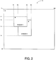
- Fig. 2 is an example of a composed frame.
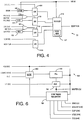
- Fig. 3 is a block diagram of a media control module and an audio module of the Fig. 1 multimedia system.
- Fig. 4 is a block diagram of a video processor circuit of the media control module of Fig. 3.
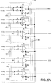
- Figs. 5A and 5B are a schematic diagram of the Fig. 4 video processor circuit.
- Fig. 6 is a block diagram of a synchronization circuit of the media control module of Fig. 3.
- Figs. 7A and 7B are a block diagram of the Fig. 6 synchronization circuit.
- Fig. 8 is a block diagram of a bus interface circuit of the Fig. 1 multimedia system.
- Fig. 9 is a schematic block diagram of a window control circuit of the Fig. 5 bus interface circuit.
- Fig. 10 is a schematic block diagram of a window priority circuit of the Fig. 7 window control module.
- Figs. 11A and 11B are a schematic block diagram of a receiver/switch circuit of the Fig. 8 bus interface circuit.
- Referring to Fig. 1,
multimedia system 10 includesmultimedia core 12,display device 14, which may be for example an all points addressable (APA) video graphics array (VGA) or high definition television (HDTV) display device,audio output device 15, which may be for example speakers or headphones,input device 16, which may be for example a keyboard or a mouse, and analog fullmotion video source 17, which may be for example, a video tape player or a video disk player.Multimedia core 12 is arranged in modules; information is transferred among modules viasystem bus 20 andmedia bus 24. Information is provided to and received frommultimedia core 12 via small computer system interface bus (SCSI) 22 andstorage bus 23. -
Multimedia core 12 includesmedia control module 30 and may includeaudio module 31,graphics accelerator module 34,processor module 36 andprogrammable receiver module 38.Modules media bus 24 via mediabus interface circuits bus interface circuits media bus 24 in response to control information; the selective access allows real time composition of the image signals. Audio signals from the media sources selectively accessmedia bus 24 in response to control information; the selective access allows real time composition of the audio signals. - A composed image signal is provided from
media bus 24 to displaydevice 14 viamedia control module 30; a composed audio signal is provided toaudio output device 15 viaaudio module 31. All input information frominput device 16 is received viamedia control module 30.Programmable receiver 38 receives analog full motion video input information directly fromvideo source 17;programmable receiver 38 may also receive electromagnetic transmissions from remote transmitters (e.g., television transmissions from television studios). The configuration ofmultimedia system 10 and ofmultimedia core 12 is meant to be representative; it is understood that the system and core configurations may be changed to satisfy a user's needs. -
System bus 20 conforms to a conventional input/output bus architecture such as the IBM Micro Channel Architecture or the IBM Family I (i.e., IBM AT) bus architecture.System bus 20 is connected between modules which transfer input/output information such asmedia control module 30,graphics accelerator module 34,processor module 36 andprogrammable receiver module 38. -
SCSI bus 22, which conforms to a conventional SCSI bus architecture, functions as a block transfer bus via which large blocks of information are transferred.SCSI bus 22 is connected directly to modules which require the transfer of large quantities of information such asprocessor module 36 andgraphics accelerator module 34 as well as to SCSI devices 40 (e.g., a SCSI tape drive, a SCSI read/write optical disk device, or a SCSI CDROM reader). BecauseSCSI bus 22 is directly connected to modules which require transfers of large quantities of information, this information need not be transferred fromSCSI bus 22 to modules which require the SCSI information viasystem bus 24. Accordingly,system bus 24 is free to perform other types of transfers. -
Storage bus 23 conforms to a conventional storage bus architecture.Storage bus 23 is connected directly betweendevices 41 which store information (e.g., a 3 1/2 inch disc drive, a hard drive or the like) andprocessor module 36. -
Media bus 24 conforms to a media bus architecture which is described herein.Media bus 24 is connected betweenmedia control module 30,audio module 31 and media bus interface circuits 39 of media sources such asgraphics accelerator module 34,processor module 36 andprogrammable receiver module 38. - By providing
system bus 20,media bus 24 andSCSI bus 22,multimedia system 10 functions as a balanced system. Each bus optimally transfers the type of information for which it is designed.
Accordingly, contention problems that arise when a bus must transfer information for which it is not designed are avoided. -
Media core 12, and more specificallymedia bus 24, composes image signals in real time for display bydisplay device 14. In other words,media core 12 combines image signals in, parallel in real time on a point by point basis for display bydisplay device 14. For the purposes of this application, "real time" is determined with reference to the sweep rate ofdisplay device 14, i.e., the speed with which information is presented bydisplay device 14. Accordingly, the speed with whichmedia bus 24 transmits information need only be as fast as the sweep rate ofdisplay device 14. - An image signal is provided by a media source to
media bus 24 via a respective media bus interface circuit 39 on a point by point basis in response to control information. A point is related to the resolution ofdisplay device 14. Accordingly, ifdisplay device 14 is a 640 by 480 VGA monitor, a point corresponds to a coordinate of the VGA monitor. Alternately, ifdisplay device 14 is a 1920 by 1035 HDTV monitor, a point corresponds to a coordinate of the HDTV monitor. - A virtual screen implementation (i.e., every module assumes that it is providing an image signal to a display) is used by
multimedia system 10 to achieve application transparency. A virtual screen implementation creates the appearance to each module of a dedicated display device. Thus, each media source which is generating an image signal generates that image signal whether or not the media source is granted access tomedia bus 24. - An image signal which is contained on
media bus 24 is received bymedia control module 30 on a point by point basis and is provided to displaydevice 14 on a point by point basis. The combination of the image signals from the media sources onmedia bus 24 provides a composed image signal which is provided tomedia control module 30.Media control module 30 adjusts the attributes (e.g., the voltage level) of the composed image signal to correspond to the attributes required bydisplay device 14 and drives an adjusted composed image signal to displaydevice 14. If no attribute adjustment were required, it is possible to provide the composed image signal directly to displaydevice 14. - Referring to Fig. 2, an example of a composed frame is shown. For the purposes of this example,
display device 14 is a VGA display device having a display resolution of 640 columns by 480 rows. The image signal which provides the background plane is provided byprocessor module 36. An image signal which is displayed in a first window (WINDOW 1) is provided byprogrammable receiver 38; this image signal is a full motion video signal. An image signal which is displayed in a second window (WINDOW 2) is provided bygraphics accelerator module 34. It is understood that the example shown is merely meant to be illustrative of the invention. - The example shown is for one frame of
display device 14. This frame is repeated multiple times per second thus allowingdisplay device 14 to provide a full motion presentation. Accordingly, the following description of a composition of a frame is repeated multiple times per second. - During composition of the frame, bus interface circuits 39 allow selective access to
media bus 24 of respective media sources in response to control information. In the preferred embodiment, the control information is provided bymedia control module 30. The control information which is provided to bus interface circuits 39 includes switching coordinate information as well as window priority information. This control information is provided when the frame is initially composed and is maintained within bus interface circuits 39 until the information for a particular module changes. I.e., multiple frames may be composed from the same switching coordinate information. If certain switching coordinate information is modified (e.g., because the display area of a particular module changes) then the modified switching coordinate information is provided to the appropriate bus interface circuit 39. This modified switching coordinate information is substituted within the appropriate bus interface circuit 39. - Synchronized media sources drive
media bus 24 in real time. Image signals are received bymedia control module 30 in real time. Thus for sources which are synchronized, there is no need to store information within video memory before displaying the information viadisplay device 14. Accordingly, the image signals that are contained onmedia bus 24 provide a composed image which is a single plane. Unsynchronized media sources provide image signals tomedia control module 30, which synchronizes these signals prior to display. - Composition of the frame shown in Fig. 2 is initiated by
bus interface circuit 39b grantingprocessor module 36 access tomedia bus 24 based upon the window priority and switching coordinate information.Processor module 36 provides an image signal tomedia bus 24 untildisplay device 14 reaches coordinate H1,V1. At this location,bus interface circuit 39b rescinds the access grant tomedia bus 24 ofprocessor module 36 and simultaneously,bus interface circuit 39c grantsprogrammable receiver module 38 access tomedia bus 24. -
Programmable receiver module 38 provides an image signal tomedia bus 24 untildisplay device 14 reaches coordinate H2,V1, at which locationbus interface circuit 39c rescinds the access grant tomedia bus 24 ofprogrammable receiver module 38 andbus interface circuit 39b grantsprocessor module 36 access tomedia bus 14. Access tomedia bus 24 continues to be interchanged betweenprocessor module 36 andprogrammable receiver module 38 at the horizontal coordinates H1 and H2 untildisplay device 14 reaches coordinate H2,V2. - At coordinate H2,V2,
bus interface circuit 39c rescinds the grant of access tomedia bus 24 ofprogrammable receiver module 38 andbus interface circuit 39a grantsgraphics accelerator module 34 access tomedia bus 24.Graphics accelerator module 34 provides an image signal tomedia bus 24 until location H3,V3, at which location access tomedia bus 24 is switched toprocessor module 36 bybus interface circuits media bus 24 continues to be exchanged betweenprocessor module 34,programmable receiver module 38, andgraphics accelerator module 34 at the horizontal coordinates H1, H2 and H3 untildisplay device 14 reaches coordinate H4,V3. - At coordinate H4,V3,
programmable receiver 38 has completed its contribution to the composition of the screen to displaydevice 14. Accordingly, for the remainder to the screen,programmable receiver 38 is no longer granted access tomedia bus 24. - At horizontal coordinates H3 and H4, access to
media bus 24 is switched betweenprocessor module 36 andgraphics accelerator module 34 untildisplay device 14 reaches coordinate H3,V4. At coordinate H3,V4, access tomedia bus 24 is returned toprocessor module 36 for the remainder of the frame. -
Media bus 24 serves as the pathway for media signals defined by the media bus architecture. The media bus architecture defines media signals for transfer of information between media sources andmedia control module 30. The media signals include image signals, control signals and audio signals. Accordingly,media bus 24 includes a plurality of video channels, a media control channel (MCC) and an audio channel. The video channels include a primary video channel (PVC), a secondary video channel (SVC), and a digital video channel (DVC). - The primary video channel is the channel via which image signals from the media sources are composed to provide a primary composed image signal to
media control module 30. The primary channel includes paths for a primary analog image signal having red green and blue components (PVC RGB), a primary color key match (PVC CKM) signal, and a primary arbitration signal (PVC ARB). The PVC RGB signal is a differential analog RGB signal which is driven directly onto the primary channel by the media sources as an analog waveform under control ofmedia control module 30. The PVC CKM signal controls video switch multiplexing inmedia control module 30; the PCKM signal is driven active low at pixel rates coincident with RGB data. The PVC ARB signal is a 4-bit one of sixteen priority arbitration signal. - The secondary video channel is the channel via which alternate or additional image signals from the media sources are composed to provide a secondary composed image signal to
media control module 30. The secondary channel includes paths for a secondary analog image signal having red, green and blue components (SVC RGB), a secondary color key match (SVC CKM) signal, and a secondary arbitration signal (SVC ARB). The SVC RGB signal is a differential analog RGB signal which is driven directly onto the secondary channel by the media sources as an analog waveform under control ofmedia control module 30. The SVC CKM signal controls video switch multiplexing inmedia control module 30; the SVC CKM signal is driven active low at pixel rates coincident with RGB data. The SVC ARB signal is a 4-bit one of sixteen priority arbitration signal. - The digital video channel is the channel via which digital video signals are transferred from a media source to
media control module 30. The digital video channel is capable of supporting high-speed live video transfers as required by HDTV and other high resolution displays as well as transfers from other digital video sources. The digital video channel includes paths for a 32-bit image signal (DIG IM), a digital clock signal, a digital HSync signal and a digital VSync signal. The DIG IM signal includes an active high 8, 16, or 24-bit RGB signal, plus an 8-bit Alpha signal, which represents a degree of transparency. The digital clock signal is provided bymedia control module 30 to clock data either throughmedia control module 30 to the media control module RGB output terminals or into a frame buffer ofmedia control module 30. The maximum clock frequency of the digital video channel is 80 MHz, thus supporting HDTV data rates of 74.25 MHz. - The media control channel provides paths for media control information which controls the transfer of information over
media bus 24. The media control channel allowsmedia control module 30 to issue device-specific control information as well as to broadcast global control information to all media sources. The media control information includes window control block data which are written to each adapter as well as vital product data and personality data which are read from each adapter whensystem 10 is initialized. The media control channel also includes paths for a source synchronization signal (SOURCE SYNC) and a system synchronization signal (SYS SYNC) as well as a master clock signal (MASTER CLK). The media control channel also includes a path for a global reference signal (V BIAS) which is provided to all media sources which are connected tomedia bus 24. - The audio channel includes paths for a high fidelity digital audio signal (AUDIO) as well as a telephony grade digital (TEL AUDIO).
- Referring to Figs. 1 and 3,
media control module 30 provides a plurality of functions formedia core 12.Media control module 30 controls composition onmedia bus 24.Media control module 30 also functions as a receiver and level converter for an image signal which is received from the primary video channel, the secondary video channel or the digital video channel.Media control module 30 also functions as a composition facility for image signals.Media control module 30 also functions as a video mixer for mixing image signals from the primary video channel, the secondary video channel and the digital video channel as well as image signals which are generated internally bymedia control module 30.Media control module 30 also functions as an image capture facility for storing images from a media source.Media control circuit 30 also functions as a display device driver circuit.Media control module 30 also functions as a synchronization signal generator for generating the synchronization signals formedia core 12.Media control module 30 also functions as a composition facility for audio signals.Media control module 30 also provides, viainput device 16, a direct user interface.Media control module 30 also interfaces withsystem bus 20 andSCSI bus 22. Some of the functions whichmedia control module 30 performs occur continuously, other functions occur as needed. However, a plurality of functions can occur simultaneously. -
Media control module 30 receives continuous data streams across the video channels ofmedia bus 24 while controlling the media sources via the media control channel.Media control module 30 includesmedia control circuit 50,bus interface circuit 51, imagesignal processor circuit 52, and frame capture circuit 54, all of which are connected via mediacontrol module bus 55.Media control module 30 also includes displaydevice adapter circuit 56,synchronization generator circuit 58. - When controlling composition of image signals on
media bus 24,media control module 30 usesmedia control circuit 50.Media control circuit 50 includes mediacontrol module microprocessor 62,memory controller 64,media system memory 66, which is dynamic random access memory (DRAM), andmenu memory 68, which is an electronically erasable programmable read only memory.Media system memory 66 holds a media control module operating system which controls the functions ofmedia control module 30;memory 66 also contains I/O handling information for interfacing withinput device 16.Menu memory 68 stores menu information which may be accessed via input device 16 (e.g., pull-down menus which are accessed via a pointing device such as a mouse). Mediacontrol module microprocessor 62 accessesmedia system memory 66 andmenu memory 68 viamemory controller 64.Memory controller 64 also controls access to any memory which may be resident on a particular bus interface circuit 39. E.g., if a new module is added tomedia core 12,media control module 30 requires media source personality data which are stored in the bus interface circuit 39 of the new module. The media source personality data are passed in a personality block via themedia control channel 30 under control ofmemory controller 64. The personality data are used by mediacontrol module microprocessor 62. - Composition of a frame is initiated by a user defining composition characteristics via
input device 16. The composition characteristics may include the desired size and shape of a window via which the image signal for a particular media source is to be displayed. Mediacontrol module microprocessor 62, in conjunction with the I/O handling information which is stored inmedia system memory 66, receives the user defined composition characteristics. Mediacontrol module microprocessor 62 then generates control information such as switching coordinate information and window priority information which is transmitted via the media control channel ofmedia bus 24 to the media sources which are connected tomedia bus 24. The media sources are granted selective access tomedia bus 24 based upon this control information. - When functioning as a receiver and level converter or when functioning as a video mixer,
media control module 30 uses imagesignal processor circuit 52. Imagesignal processor circuit 52 includesdisplay controller 70 as well asmixer circuit 72.Display controller 70 functions as a interface circuit between frame capture circuit 54 andmixer circuit 72 because, by using frame capture circuit 54,media control module 30 may function as a source of an image signal. In addition to functioning as an interface between frame capture circuit 54 andmixer 72,display controller 70 also manages acquisition and display of images which are stored inframe capture circuit 52.Display controller 70 also manages other display functions such as background color flood in which the background presentation ofdisplay device 14 is set to a certain color.Display controller 70 also controls the fade level of selected frame buffer images (e.g., the menu image or a captured image) under control of mediacontrol module microprocessor 62. - When functioning only as a receiver and level converter,
mixer circuit 72 of imagesignal processor circuit 52 receives either the PVC RGB signal, the SVC RGB signal or the DIG IM signal frommedia bus 24.Mixer circuit 72 levels the received image signal to provide a composed image signal (COMP RGB) which is has a constant base output level, e.g., a constant black level. - When functioning as a leveling circuit and a mixer circuit,
mixer circuit 72 of imagesignal processor circuit 52 receives one or more of the PVC RGB and PVC CKM signals, the SVC RGB and SVC CKM signals, and the DIG IM signal frommedia bus 24, as well as a capture signal (MCM RGB) from frame capture circuit 54.Mixer circuit 72 mixes these signals under control ofdisplay controller 70 and levels the mixed signal to provide the COMP RGB signal. - When functioning as a composition facility,
media control module 30 usesmixer circuit 72 in conjunction withmedia control circuit 50. During composition withinmedia control module 30,mixer circuit 72 switches on a point by point basis between the PVC RGB, SVC RGB and DIG IM signals as well as a frame capture signal which is provided by frame capture circuit 54 to provide the COMP RGB signal.Display controller 70 controls the switching based upon information which is provided bymedia control circuit 50.Media control circuit 50 provides this information in response to user defined composition characteristics. - When functioning as an image capture facility,
media control module 30 uses frame capture circuit 54. Frame capture circuit 54 includes framebuffer control circuit 78,frame buffer 80, which is video random access memory (VRAM),switch circuit 82 andfader circuit 84.Switch circuit 82 includesimage switch 86, analog to digital (A/D)converter 88 andbuffer circuit 90.Fader circuit 84 includes digital toanalog converters fader circuit 96. Frame capture circuit 54 receives the synchronization signals PVC SYNC, the SVC SYNC, the SYS SYNC. Frame capture circuit 54 also receives the PVC RGB signal, the SVC RGB signal and the DIG IM signal frommedia bus 24 and a composed image signal from imagesignal processor circuit 52 and selectively stores one of these signals in response to control information which is provided by mediacontrol module microprocessor 62 viamedia control bus 55 to capture a frame of information. When storing the frame capture signal, frame capture circuit is synchronized by the synchronization signal. Frame capture circuit 54 may provide to imagesignal processor circuit 52 the analog equivalent of the capture signal as the MCM RGB. - Frame capture circuit 54 is used to capture images, to receive image signals from non-genlocked (i.e., unsynchronized) sources and to provide menu information. Accordingly,
frame buffer 80 includes both an image capture plane as well as a menu plane. The image capture plane is capable of storing four captured images. The menu capture plane is capable of storing menu information which is received frommenu memory 68. - When capturing an image, image signals are selectively provided to
frame buffer 80 viaswitch 86. The analog image signal is converted to an equivalent digital signal via analog todigital converter 88 prior to being provided to switch 86; the switched image is buffered viabuffer 90.Buffer 90 is used to synchronize information which is provided to framebuffer 80 because the information may not be genlocked (i.e., synchronized) or may have timing skews due to composition or bus transmission. Image signals are provided to framebuffer 80 via serial ports. When writing to framebuffer 80,frame buffer 80 is synchronized with the source of the information. When reading fromframe buffer 80,frame buffer 80 is synchronized with the SYS SYNC signal. - When presenting menu information, menu information which is stored in
menu memory 68 is provided, via mediacontrol module bus 55, to a random access port offrame buffer 80 by mediacontrol module microprocessor 62. The menu information is stored in the menu plane offrame buffer 80. The menu information which is stored in the menu plane is then presented viamixer circuit 72. - When functioning as a display device driver,
media control module 30 uses displaydevice adapter circuit 56. Displaydevice adapter circuit 56 includes 75ohm driver circuit 98 and RGB toNTSC converter circuit 100. Displaydevice adapter circuit 56 receives the composed image signal COMP RGB from imagesignal processor circuit 52 and the SYS SYNC signal fromsynchronization generator circuit 58. Displaydevice adapter circuit 56 generates via 75ohm driver circuit 98 an RGB signal (RGB OUT), which is capable of driving a VGA monitor Displaydevice adapter circuit 56 generates via RGB to NTSC converter circuit 102 a composite NTSC signal (NTSC OUT), which is capable of driving a video monitor, video cassette recorder or other device which requires a direct composite baseband video input signal. - When functioning as a synchronization signal generator,
media control module 30 usessynchronization generator circuit 58.Synchronization generator circuit 58 includesprogrammable sync generator 104 andoscillator 106.Synchronization generator circuit 58 receives the SOURCE SYNC signal, which is receive viamedia bus 24 from a media source as selected by mediacontrol module microprocessor 62, an external house synchronization signal (EHS), which may be externally provided tomedia control module 30, and an internal synchronization signal (INT SYNC) which is generated byoscillator 106 ofsynchronization generator circuit 58. The EHS signal may be a synchronization signal which includes separate horizontal and vertical components (EHS HSYNC, EHS VSYNC), a composite synchronization signal (i.e., a single signal which includes both horizontal and vertical components) or a black burst synchronization signal (i.e., a composite signal minus any video).Synchronization generator circuit 58 provides the SYS SYNC signal and the WIND CLK signal to the media control channel as well as a master clock signal (MASTER), which is the clock signal used internally bymedia control module 30, a blanking signal (BLANKING), a media control module synchronization signal (MCM SYNC), a display synchronization signal (DISP SYNC) and an NTSC composite synchronization signal (NTSC SYNC). The WIND CLK signal is provided to all media sources, thus allowing synchronous switching during composition. The MASTER signal is the clock signal used internally bymedia control module 30. The BLANKING signal, which includes a horizontal blanking signal (H BLANKING) and a vertical blanking signal (V BLANKING), controls whendisplay device 14 is not illuminated such as during the retrace of a display device which scans an image signal. The MCM SYNC signal, which includes a horizontal component (MCM HSYNC) and a vertical component (MCM VSYNC), controls the display timing formedia control module 30. The NTSC SYNC signal is the signal which is a synchronization signal which is compatible with the standard U.S. NTSC format. The DISP SYNC signal, which includes a horizontal component (DISP HSYNC) and a vertical component (DISP VSYNC), controls the horizontal and vertical synchronization pulses which VGA type display devices require. - When functioning as a direct user interface, input signals which are provided by
input device 16 are received by mediacontrol module microprocessor 62 via mediacontrol module bus 55. These input signals may be used to generate menu presentations, in which case the input signals are used directly bymedia control module 30. These input signals may also be intended for another module such asprocessor module 36, in which case the input signals are received bymedia control module 30 and then provided toprocessor module 36 viasystem bus 20. When the input signals are intended for another module,media control module 30 still provides the necessary support to interpret the input signals before providing the input signals to the appropriate module. - When interfacing with
system bus 20 andSCSI bus 22,media control channel 30 usesbus interface circuit 51.Bus interface circuit 51 also allowsmedia control channel 30 to interface with the media control channel ofmedia bus 24. - Referring to Fig. 4,
mixer circuit 72 usesswitches summer circuit 116.Switches display controller 70 and the PVC CKM and SVC CKM signals which are provided by respective media sources.Switches display controller 70.Summer circuit 116 receives the image signals provided byswitches Summer circuit 116 also includes abias generator circuit 117 which generates the reference voltage V BIAS. - The PVC RGB signal, which is received from
media bus 24 byprimary receiver circuit 118, is provided tosummer circuit 116 based upon the PVC CKM signal, which is received frommedia bus 24, and an inhibit primary video signal (INH PVC) signal, which is provided bydisplay controller 70.Switch 110 provides the PVC RGB image signal tosummer circuit 116 when both the PVC CKM signal and the INH PVC are inactive as determined byOR gate 119. ORgate 119 provides a select primary channel (PVC SEL) to switch 110. Accordingly, the PVC RGB signal is provided tosummer circuit 116 unless the primary video channel is inhibited or a color key match corresponds to the PVC RGB signal for the particular coordinate. - The SVC RGB signal, which is received from
media bus 24 bysecondary receiver circuit 120, is provided tosummer circuit 116 based upon the SVC CKM signal, which is received frommedia bus 24, and an inhibit secondary video signal (INH SVC), which is provided bydisplay controller 70.Switch 112 provides the SVC RGB image signal tosummer circuit 116 when both the SVC CKM signal and the INH PVC signal are inactive as determined byOR gate 121. ORgate 121 provides a select secondary channel (SVC SEL) to switch 112. Accordingly, the SVC RGB signal is provided tosummer circuit 116 unless the secondary video channel is inhibited or a color key match corresponds to the SVC RGB signal for the particular coordinate. - Digital to
RGB converter 122 provides a signal (DIG RGB), which is the leveled RGB equivalent of the DIG IM signal, to switch 114.
Converter 122 receives the V BIAS signal, and adjusts the level of the DIG RGB signal appropriately.Switch 114 provides the DIG RGB signal tosummer circuit 116 when the select digital image signal DIG SEL, which is provided bydisplay controller 70, is active. -
Switch 113 provides the MCM RGB signal tosummer circuit 116 when the MCM SEL signal, which is provided bydisplay controller 70, is active. - Referring to Figs. 5A and 5B,
mixer circuit 72 includesprimary receiver circuit 118,secondary receiver circuit 120,switch circuits summer circuit 116, as well asregulator circuit 122 andbias generator circuit 117. -
Primary receiver circuit 118 includes three differential receiver circuits 124(r), 124(g), 124(b) (referred to generally as differential receiver circuit 124) which receive a respective component of the PVC RGB signal. Receiver circuit 124(r) receives the differential red component signal of the PVC RGB signal (PVC R) and provides a single ended primary red component signal (PRI R). Receiver circuit 124(g) receives the differential green component signal of the PVC RGB signal (PVC G) and provides a single ended primary green component signal (PRI G). Receiver circuit 124(b) receives the differential blue component signal of the PVC RGB signal (PVC B) and provides a single ended primary blue component signal (PRI B). Each receiver circuit 124(r), 124(g), 124(b) includes a high speed voltage mode operational amplifier (available under the trade designation HA-2540 from Harris, Inc.) which is configured to operate as a differential receiver. Eachcomponent receiver circuit 124 is provided with the V BIAS reference signal. -
Secondary receiver circuit 120 includes three differential receiver circuits 128(r), 128(g), 128(b) (referred to generally as differential receiver circuit 128) which receive a respective component of the SVC RGB signal. Receiver circuit 128(r) receives the differential red component signal of the SVC RGB signal (SVC R) and provides a single ended secondary red component signal (SEC R). Receiver circuit 128(g) receives the differential green component signal of the SVC RGB signal (SVC G) and provides a single ended secondary green component signal (SEC G). Receiver circuit 128(b) receives the differential blue component signal of the SVC RGB signal (SVC B) and provides a single ended secondary blue component signal (SEC B). Each receiver circuit 128(r), 128(g), 128(b) includes a high speed voltage mode operational amplifier (available under the trade designation HA-2540 from Harris, Inc.) which is configured to operate as a differential receiver. Eachcomponent receiver circuit 128 is provided with the V BIAS reference signal. - Because each
component receiver circuit - Each
switch circuit amplifier circuit 130 of a component of the PRI RGB, SEC RGB, DIG RGB and MCM RGB signals. The component switches are high speed analog switches (available from Texas Instruments, Inc. under the trade designation TLC 4066I); each switch allows selective access to a component summingamplifier circuit 130. -
Switches inverter circuit 131 prior to being provided to the switches. -
Summer circuit 116 includes three component summing amplifier circuits 130(r), 130(g), 130(b) (referred to generally as component summing amplifier circuit 130). Red component summing amplifier circuit 130(r) receives the PRI R signal, the SEC R signal, the MCM R signal and the DIG R signal as red component input signals and provides the red component of the COMP RGB signal (COMP R), which is the sum of the red component input signals. Green component summing amplifier circuit 130(g) receives the PRI G signal, the SEC G signal, the MCM G signal and the DIG G signal as green component input signals and provides the green component of the COMP RGB signal (COMP G), which is the sum of the green component input signals. Blue component summing amplifier circuit 130(b) receives the PRI B signal, the SEC B signal, the MCM B signal and the DIG B signal as blue component input signals and provides the blue component of the COMP RGB signal (COMP B), which is the sum of the blue component input signals. Each component summingamplifier circuit 130 includes a high speed operational amplifier (available from Harris, Inc. under the trade designation HA-2540) which is configured as a unity gain summing amplifier. Each component summing amplifier circuit is provided with the V BIAS reference signal. Accordingly, each component summing amplifier circuit output signal is level set based upon the same system reference voltage. -
Regulator circuit 122 includes a three terminal voltage adjustable voltage regulator (e.g., a LM 317 available from National Semiconductor, Inc.). The voltage regulator is biased by resistors to provide a regulated voltage of 10 volts.Regulator circuit 122 includes diodes which provide a shunt path to discharge the capacitors when power tosystem 10 is removed. -
Bias generator circuit 117 divides the regulated voltage by half to provide the V BIAS reference signal which is a low-impedance reference voltage. The low impedance voltage decreases the susceptibility of the V BIAS signal to interference.Bias generator circuit 117 includes an operational amplifier which is configured as a low impedance voltage follower and a transistor which allowsbias generator circuit 117 to provide current if necessary. - Referring to Fig. 6,
programmable sync generator 104 includesinput multiplexer 150, mainphase lock loop 152,output multiplexer 154, andsync timing generator 156.Input multiplexer 150 receives the SOURCE SYNC signal and the EHS signal and provides a selected source synchronization signal (SEL SOURCE SYNC) signal to phaselock loop 152 andsync timing generator 156.Phase lock loop 152 receives the SEL SOURCE SYNC signal and provides a phase locked synchronization signal (SYNC CLK) tooutput multiplexer 154.Output multiplexer 154 receives the SYNC CLK signal and the INT SYNC signal and provides the MASTER CLK signal to synctiming generator 156.Sync timing generator 156 receives the MASTER CLK signal and the SEL SOURCE SYNC signal and provides the BLANKING signal, the MCM INT SYNC signal, the SYS SYNC signal, the NTSC COMP SYNC signal, the WIND CLK signal and the DISPLAY SYNC signal. - More specifically, referring the Figs. 7A and 7B,
input multiplexer 150 includes switches 160(h), 160(v) which receive the SOURCE HSYNC and SOURCE VSYNC signals, respectively. Switches 160(h), 160(v) are controlled via the SYNC INPUT SELECT signal which is provided by mediacontrol module microprocessor 62.Input multiplexer 150 also includes switches 162(h), 162(v) which receive the EHS HSYNC and EHS VSYNC signals, respectively. The EHS VSYNC signal is also provided to vertical synchronizationsignal detector circuit 164 which detects the presence of a vertical sync signal and provides a control input signal to switchcontrol circuit 166 which also receives the SYNC INPUT SELECT signal. The EHS HSYNC signal path, via which the composite synchronization signal or the black burst synchronization signal is provided tomultiplexer 150, is also connected to synchronizationsignal separator circuit 168. Synchronizationsignal separator circuit 168 separates the composite synchronization signal or the black burst synchronization signal into horizontal and vertical components. The horizontal and vertical components of the separated signal are provided tocomposite switch 170 which provides horizontal and vertical component output signals. The vertical component of the separated signal provided byseparator circuit 168 is provided to switchcontrol circuit 166.Switch control circuit 166 controls the activation of switches 162(h), 162(v) andcomposite switch 170 based upon the horizontal component of the separated signal, the control input signal provided by verticalsynchronization signal detector 164 and the SYNC INPUT SELECT signal. The output signals of switches 160(h), 162(h) and the horizontal component ofcomposite switch 170 are tied together to provide the SEL SOURCE HSYNC signal. The output signals of switches 160(v), 162(v) and the vertical component ofcomposite switch 170 are tied together to provide the SEL SOURCE VSYNC signal. The SEL SOURCE HSYNC signal is provided to mainphase lock loop 152. - Main
phase lock loop 152 functions as a master system clock synthesizer. A phase lock loop control signal (PLL CNT) is provided via mediacontrol module bus 55 from mediacontrol module microprocessor 62 toprogrammable dividers Phase detector 176 receives the SEL SOURCE HSYNC signal and detects its phase.Loop filter 178 receives the output signal ofphase detector 176 and determines acquisition and tracking filter characteristics of the phase lock loop. Voltage controlledoscillator 179 receives a DC voltage which is provided byloop filter 178 and provides a frequency based upon this voltage.Programmable dividers phase lock loop 152 provides a master video timing clock (SYNC CLK). The SYNC CLK signal is the basis for all video pixel and display timings. The SYNC CLK signal is provided tooutput multiplexer 154. -
Output multiplexer 154 provides an alternate fixed frequency master clock signal based upon either the SYNC CLK signal or the INT SYNC signal. More specifically, mediacontrol module microprocessor 62 instructsoutput multiplexer 154 to select the SYNC CLK signal for the timing source forsystem 10 unless a video source is not selected to provide a synchronization signal and an external synchronization signal is unavailable. For this condition,media control module 30 instructsmultiplexer 154 to select the INT SYNC signal as the timing source for the system. This condition may exist whensystem 10 is first activated and thus no source has been yet chosen. In this case, the INT SYNC signal provides a timing reference so that the menus which are generated bymedia control module 30 may be displayed. The MASTER CLK signal is provided to programmablevideo synchronization generator 156. - Programmable
video sync generator 156 includeshorizontal counter circuit 180 andvertical counter circuit 182 which are programmed by mediacontrol module microprocessor 62 to provide the horizontal and vertical components of the timing signals which support the display device in use. These timing signals are used bydisplay device 14 and as well as displaydevice adapter circuit 56 ofmedia control module 30. - Programmable
video sync generator 156 also includes 14.318MHz synthesizer 184 which provides a signal which clocksNTSC timing generator 186.Synthesizer 184 uses a phase lock loop to derive this signal based upon the SYS HSYNC signal so that whensystem 10 is operating in a genlocked mode, the NTSC COMP SYNC output signal is synchronized with the media source synchronization signal. If, however,system 10 is synchronized with the INT SYNC signal, the NTSC COMP SYNC signal is synchronized with the internal synchronization signal. In either case, the NTSC COMP SYNC signal is synchronized with the signal which synchronizessystem 10. - Programmable
video sync generator 156 also includes programmablewindow clock circuit 188 which provides the WIND CLK signal. The WIND CLK signal is used by all of the media sources to synchronize their respective windowing circuits. The frequency of the WIND CLK signal is programmed by mediacontrol module microprocessor 62 based upon the resolution requirements of any application software which is being used by the media sources. - Programmable
video sync generator 156 also includes monitorsync polarity encoder 190 which a provides the DISPLAY SYNC signal based upon the SYS SYNC signal. The DISP HSYNC and DISP VSYNC signals include horizontal and vertical synchronization pulses which are used by standard VGA type display devices. - Referring to Fig. 8, bus interface circuit 39 for a corresponding module is shown. Interface circuit 39 includes
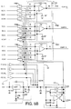
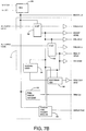
control circuit 200 as well as analog imagesignal processor circuit 202,digital video switch 206,audio analog switch 208, and syncanalog switch 210. Analog imagesignal processor circuit 202 receives an analog image signal (ANALOG IMAGE) from a media source and switches this signal onto either the primary video channel and secondary video channel under control ofcontrol circuit 200.Digital video switch 206 receives a digital image signal (DIGITAL IMAGE) and switches this signal onto the digital video channel.Audio switch 210 receives an audio signal and switches this signal onto the audio channel.Sync analog switch 208 receives source synchronization information and switches this information onto a portion of the media control channel. -
Control circuit 200 receives control information from the media control channel ofmedia bus 24 and provides control signals toprocessor circuit 202 and switches 206, 208, 210. The control information includes window control block information such as the switching coordinate signals HSTART, HSTOP, VSTART and VSTOP, the 4-bit window priority signal, WP, and attribute parameter signals. The attribute parameter signals include the primary video channel enable signal, PVC EN, the secondary video channel enable signal, SVC EN, the superimpose signal, S, the full window signal, FW, the fade in signal, FIN, the fade out signal, FOUT, the 8-bit fade level signal, FLEVEL, and the fade step size signal STEP. The window control block information is stored in windowcontrol block memory 214. -
Control circuit 200 controls the activation and deactivation ofprocessor 202 and switch 206 via analogwindow control circuit 212 and digitalwindow control circuit 216, respectively. Accordingly,control circuit 200 controls access tomedia bus 24, and thus composition of the ANALOG IMAGE signal and the DIGITAL IMAGE signal of a media source.Control circuit 200 controls the activation and deactivation ofprocessor 202 and switch 206 based upon the switching coordinate information and the window priority information which is received frommedia control module 30. In a preferred embodiment, the window block information is received bycontrol circuit 200 when a frame is initially composed. This information is stored in coordinatememory 214 ofcontrol circuit 200 until the information is updated bymedia control module 30. The stored information is provided to analogwindow control circuit 212 and digitalwindow control circuit 216. Analogwindow control circuit 212 and digitalwindow control circuit 216 include similar circuitry. However, because digitalwindow control circuit 216 controls access to one video channel, the digital video channel, while analogwindow control circuit 214 control access to two video channels, the primary video channel and the secondary video channel, some circuitry of digitalwindow control circuit 216 is duplicated for analogwindow control circuit 214. -
Control circuit 200 also controls activation and deactivation ofaudio switch 210. Accordingly,control circuit 200 controls access tomedia bus 24 of the audio information of a particular module.
Control circuit 200 also controls activation and deactivation ofanalog sync switch 208 based upon synchronization control information which is provided by mediacontrol module microprocessor 62 via the media control channel. Accordingly,control circuit 200 controls access tomedia bus 24 of the synchronization information of a particular module. The synchronization information of the module which is granted access tomedia bus 24 becomes the SOURCE SYNC signal. - It is understood that a particular media source need not provide all types of media signals. For example, a media source could provide an analog image signal without providing a digital image signal or vice versa. Also, for example, a media source may provide an analog image signal without providing an audio signal. A bus interface circuit 39 for a particular media source need only be configured to allow selective access to
bus 24 for the types of media signals which the particular media source provides. For example, a bus interface circuit 39 for a media source which provides an analog image signal without providing a digital image signal need not includedigital switch 206 or digitalwindow control circuit 216. - Referring to Fig. 9, in addition to the information which is stored in window
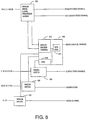
control block memory 214, analogwindow control circuit 212 receives the WIND CLK signal frombus 24. Analogwindow control circuit 212 provides the 4-bit PVC ARB signal and the 4-bit SVC ARB signal tomedia bus 24 as well as a primary video channel enable control signal (GATE PVC) and a secondary video channel enable control signal (GATE SVC) to analog imagesignal processor circuit 202. - Analog
window control circuit 212 includescomparison circuit 220,timing circuit 222,window priority circuit 224 and fadecircuit 226. -
Comparison circuit 220 includesregisters Register 230 provides a clocked HSTART signal tocomparator 238.Register 232 provides a clocked HSTOP signal tocomparator 240.Comparators counter 242 oftiming circuit 222.Register 234 provides a clock VSTART signal tocomparator 244 and register 236 provides a clocked VSTOP signal tocomparator 246.Comparators counter 248 oftiming circuit 222. -
Timing circuit 222 provides the VCNT and HCNT signals based upon the WIND CLK signal which is provided bysynchronization generator circuit 58 ofmedia control module 30.Counters media bus 24 and provide the HCNT and VCNT signals, respectively. The HCNT and VCNT signals indicate a display coordinate ofdisplay device 14. The WIND CLK signal is also used to clock set/reset latches 252, 254 as well aswindow priority circuit 224. -
Comparator 238 provides a horizontal set signal to the set input terminal offlip flop 252;comparator 240 provides a horizontal reset signal to the reset input terminal offlip flop latch 252. Accordingly, whencomparator 238 detects a match between the HCNT signal and the HSTART signal,flip flop 252 is set. Whencomparator 240 detects a match between the HCNT signal and the HSTOP signal,flip flop 252 is reset. Accordingly, whenflip flop 252 is set, the current display coordinate is within the horizontal window coordinates as set by the HSTART and HSTOP signals.Flip flop 252 provides a primary video channel window compete signal (PVC COMPETE) towindow priority circuit 224. The PVC COMPETE signal indicates when the current display coordinate, is within the window coordinates set forth by the HSTART, HSTOP, VSTART, and VSTOP signals and the primary video channel is enabled. -
Comparator 244 provides a vertical set signal to the set input terminal offlip flop 254;comparator 246 provides a vertical reset signal to the reset input terminal offlip flop 254. Whencomparator 244 detects a match between the VCNT signal and the VSTART signal,flip flop 254 is set. Whencomparator 246 detects a match between the VCNT signal and the VSTOP signal,flip flop 254 is reset.Flip flop 254 provides a window active signal (WACTIVE) to ANDgate 255. The WACTIVE signal indicates when the current coordinate is within the vertical coordinates defined by the VSTART and VSTOP signals. - AND
gate 255 provides a primary channel enabled signal to flipflop 252. ANDgate 255 also receives the HSYNC signal and the PVC EN signal. Accordingly, when the WACTIVE signal is inactive, indicating that a scan is not within the vertical start and stop coordinates, or when the PVC EN signal is inactive, indicating that the primary video channel is not enabled,flip flop 252 is reset and provides an inactive PVC COMPETE signal towindow priority circuit 224. Because the HSYNC signal is provided to ANDgate 255, the primary channel enabled signal may be provided to flipflop 252 on a point by point basis. -
Comparator 238 also provides the horizontal set signal to the set input terminal offlip flop 256;comparator 240 also provides the horizontal reset signal to the reset input terminal offlip flop latch 256. Whencomparator 238 detects a match between the HCNT signal and the HSTART signal,flip flop 256 is set. Whencomparator 240 detects a match between the HCNT signal and the HSTOP signal,flip flop 256 is reset. Accordingly, whenflip flop 252 is set, the current display coordinate is within the horizontal window coordinates as set by the HSTART and HSTOP signals.Flip flop 256 provides a secondary video channel window compete signal (SVC COMPETE) towindow priority circuit 224. The SVC COMPETE signal indicates when the current display coordinate, is within the window coordinates set forth by the HSTART, HSTOP, VSTART, and VSTOP signals and the secondary video channel is enabled. - The WACTIVE signal which is generated by
flip flop 254 is also provided to AND gate 257. AND gate 257 provides a secondary channel enabled signal to flipflop 252. AND gate 257 also receives the HSYNC signal and the SVC EN signal. Accordingly, when the WACTIVE signal is inactive, indicating that a scan is not within the vertical start and stop coordinates, or when the SVC EN signal is inactive, indicating that the secondary video channel is not enabledflip flop 256 is reset and provides an inactive SVC COMPETE signal towindow priority circuit 224. Because the HSYNC signal is provided to AND gate 257, the secondary channel enabled signal may be provided to flipflop 256 on a point by point basis. -
Window priority circuit 224 arbitrates for access tomedia bus 24, controls access tomedia bus 24 and controls superimposition of the primary and secondary video channels.Window priority circuit 224 receives the PVC COMPETE and SVC COMPETE signals fromcomparison circuit 220, the WIND CLK signal, the PVC EN and SVC EN enable signals, and the PVC ARB and SVC ARB arbitration signals frombus 24 as well as the WP signal, the S signal, and the FW signal which are stored in register 257.Window priority circuit 224 includes primary window priority circuit 258(p) and secondary window priority circuit 258(s) which provide the GATE PVC signal and the GATE SVC signal, respectively. But for the signals which are received by and provided by primary and secondary window priority circuits 258(p), 258(s), these circuits are identical. - When primary window priority circuit 224(p) receives an active PVC COMPETE signal, an active PVC EN signal, and wins control of
bus 24 via arbitration, then window priority circuit 224(p) generates an active GATE PVC signal which activates the primary switch ofprocessor circuit 202, thus allowing the ANALOG IMAGE signal to be provided to the primary video channel ofbus 24. When secondary window priority circuit 224(s) receives an active SVC COMPETE signal, an active SVC EN signal, and wins control ofbus 24 via arbitration, then secondary window priority circuit 224(s) generates an active GATE SVC signal which activates the secondary switch ofprocessor circuit 202 thus allowing the ANALOG IMAGE signal to be provided to the secondary video channel ofbus 24. -
Window control circuit 200 also includes afade circuit 226 which controls the amplitude of the drivers of analog imagesignal processor circuit 202 based upon fade signals FIN FOUT, FLEVEL and STEP. More specifically, fadesignal generator circuit 258 generates a serial FADE DATA signal based upon the FLEVEL and STEP signals. The FADE DATA signal is updated each frame or multiple thereof by incrementing or decrementing fadesignal generator circuit 258 from a certain amplitude level, as set forth by the FLEVEL signal, by a certain step size as set forth by the STEP signal. The update is repeated until a minimum or maximum fade level is reached. The FADE DATA signal is provided to analog imagesignal processor circuit 202. The FIN and FOUT signals determine whether to fade into a particular image or out of a particular image. - Referring to Fig. 10, primary window priority circuit 258(p) includes
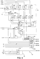
arbitration circuit 260 and source enablecircuit 262.Arbitration circuit 260 receives the PVC COMPETE signal fromcomparison circuit 220, the 4-bit WP signal from register 225 and the 4-bit PVC ARB signal and the WIND CLK signal frombus 24 and arbitrates for control ofbus 24. Source enablecircuit 262 receives the S signal and the FW signal from windowcontrol block memory 214, the WIND CLK signal and the PVC EN signal frombus 24, and arbitration signals fromarbitration circuit 260 and provides the GATE PVC signal. -
Arbitration circuit 260 provides a four stage pipelined structure in which four points are simultaneously arbitrated. The four stage arbitration is possible because information which is provided tobus 24 is display position dependent. Accordingly, identifying the current coordinate location of information which is provided tobus 24 allows identification of future coordinate locations. All HSTART and HSTOP window switching coordinates are thus set four coordinates ahead of the desired display coordinate under software control bymedia control module 30. - During composition of a frame, arbitration begins four cycles before the coordinate location for which the arbitration is being performed. During arbitration for a particular coordinate location, the PVC COMPETE signal corresponding to that location is provided to
arbitration circuit 260. This PVC COMPETE signal is pipelined througharbitration circuit 260 so that whendisplay device 14 is at the corresponding coordinate location, a signal which is derived from the PVC COMPETE signal contributes to the generation of the GATE signal. - More specifically, during arbitration for the first coordinate location, the PVC COMPETE signal corresponding to the first coordinate location and the most significant bit of the WP signal, WP(3) (a number in parentheticals indicates a corresponding bit of a multibit signal), are provided to
NAND gate 270. If both the PVC COMPETE signal and the WP(3) signal are active, thenNAND gate 270 drives the ARB(3) signal active. If either the PVC COMPETE signal or the WP(3) signal are inactive thenNAND gate 270 does not drive the ARB(3) signal active. The ARB(3) signal may also be driven active by any other media source which is arbitrating forbus 24. - The WP(3) bit and the ARB(3) bit are provided to OR
gate 272, which provides a more significant arbitration bit indication signal to ANDgate 274. ANDgate 274 also receives the PVC COMPETE signal. ANDgate 274 provides a compete indication signal toD flip flop 276 which provides a pipelined compete signal (PVC COMPETE2) toNAND gate 278.Flip flop 276 is clocked by the WIND CLK signal.NAND gate 278 also receives the WP(2) bit. If both the PVC COMPETE2 signal and the WP(2) bit are active, thenNAND gate 278 drives the ARB(2) bit active. If either the PVC COMPETE2 signal or the WP(2) bit are inactive thenNAND gate 278 does not drive the ARB(2) bit active. The ARB(2) bit may also be driven active by any other media source which is arbitrating forbus 24. - The WP(2) bit and the ARB(2) bit are provided to OR
gate 280, which provides a more significant arbitration bit indication signal to ANDgate 282. ANDgate 282 also receives the PVC COMPETE2 signal. ANDgate 282 provides a compete indication signal toD flip flop 284 which provides a pipelined compete signal (PVC COMPETE3) toNAND gate 286.Flip flop 284 is clocked by the WIND CLK signal.NAND gate 286 also receives the WP(1) bit. If both the PVC COMPETE3 signal and the WP(1) bit are active, thenNAND gate 286 drives the ARB(1) bit active. If either the PVC COMPETE3 signal or the WP(1) bit are inactive thenNAND gate 286 does not drive the ARB(1) bit active. The ARB(1) bit may also be driven active by any other media source which is arbitrating forbus 24. - The WP(1) bit and the ARB(1) bit are provided to OR
gate 288, which provides a more significant arbitration bit indication signal to ANDgate 290. ANDgate 290 also receives the PVC COMPETE3 signal. ANDgate 290 provides a compete indication signal toD flip flop 292 which provides a pipelined compete signal (PVC COMPETE4) toNAND gate 294.Flip flop 290 is clocked by the WIND CLK signal.NAND gate 294 also receives the WP(0) bit. If both the PVC COMPETE4 signal and the WP(0) bit are active, thenNAND gate 294 drives the ARB(0) bit active. If either the PVC COMPETE4 signal or the WP(0) bit are inactive thenNAND gate 294 does not drive the ARB(0) bit active. The ARB(0) bit may also be driven active by any other media source which is arbitrating forbus 24. - The ARB(0) bit is provided to AND
gate 296 which also receives the PVC COMPETE4 signal. ANDgate 296 provides an arbitration bit indication signal to NORgate 300. If the PVC COMPETE4 signal is active and the ARB(0) bit is inactive, then ANDgate 296 provides an active arbitration bit indication signal to NORgate 300. If NORgate 300 receives an active arbitration bit indication signal, then it provides an active gate signal to flipflop 304. If either the PVC COMPETE4 signal is inactive or the ARB(0) bit is active then ANDgate 296 provides an inactive arbitration bit indication signal to NORgate 300. - The WP(0) bit is provided to AND
gate 302 which also receives the PVC COMPETE4 signal. ANDgate 302 provides a window priority bit indication signal to NORgate 300. If the WP(0) signal is active and the PVC COMPETE4 bit is active, then ANDgate 302 provides an active window priority bit indication signal to NORgate 300. If NORgate 300 receives an active window priority bit indication signal, then it provides an active gate signal to flipflop 304. If either the WP(0) signal is inactive or the PVC COMPETE4 bit is inactive then ANDgate 296 provides an inactive window priority bit indication signal to NORgate 300. - NOR
gate 300 provides an unclocked gate signal toD flip flop 304 which is clocked by the WIND CLK signal.Flip flop 304 is controlled by the PVC EN signal which is provided to the set input terminal offlip flop 304. Accordingly, if the PVC EN signal is active, then flipflop 304 passes the unclocked gate signal at the next rising edge of the WIND CLK signal to provide the GATE PVC signal. If the PVC EN signal is inactive then the GATE PVC signal remains inactive. - AND
gate 306, which receives the S signal as well as a PVC COMPETE signal which is delayed three WIND CLK signal clock cycles bydelay circuit 307, provides an active superimpose enabled signal to NORgate 300 when the S signal is active and the PVC COMPETE signal is active. An active superimpose enabled signal causes NORgate 300 to provide an active gate signal to flipflop 304. - AND
gate 308, which receives the FW signal, provides an active full window enabled signal to NORgate 300 when the FW signal is active. An active full window enabled signal causes NORgate 300 to provide an active gate signal to flipflop 304. - Referring to Figs. 11A and 11B, analog image
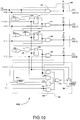
signal processor circuit 202 is shown. Analog imagesignal processor circuit 202 receives the red, green and blue components of the ANALOG IMAGE signal as well as the FADE CLK, FADE DATA and FADE EN fade signals and the HSYNC signal and provides the differentially driven PVC RGB and SVC RGB signals. Analog imagesignal processor circuit 202 includes analog imagesignal conditioner circuit 350,driver circuit 352 andswitch circuit 354. - Analog image
signal conditioner circuit 350 includes red component conditioner circuit 356(r), green component conditioner circuit 356(g), and blue component conditioner circuit 356(b). These circuits are similar and are generally referred to ascomponent conditioner circuit 356. Eachcomponent conditioner circuit 356 includes video amplifier circuit 358 (e.g., a LM 1201 available from National Semiconductor, Inc.) as well as three-input serial digital to analog converter (DAC) 360 (e.g., a MC144111 available from Motorola Corp.). -
Video amplifier circuit 358 receives a component of the ANALOG IMAGE signal, conditions this component and provides a conditioned component signal todriver circuit 352. (E.g.,video amplifier circuit 358 of red component conditioner circuit 356(r) provides a COND R signal.) The conditions whichvideo amplifier circuit 358 control include the black level of the component and the fade/gain level of the component. - The black level of the component is based upon the V BIAS signal which is provided by
bias generator circuit 117 ofmedia control module 30. This is the same V BIAS signal which sets the black level ofmedia control module 30. Because bus interface circuit 39 uses the same reference signal asmedia control module 30, a standard black level is produced regardless of which media source provides its image signal tobus 24. - The fade level of the component is based upon a voltage level which is provided by
DAC 360 tovideo amplifier circuit 358.DAC 360 receives the FADE CLK signal, the FADE DATA signal and the FADE EN signal and provides a voltage indicative of fade level tovideo amplifier circuit 358. -
Driver circuit 352 includes red component driver circuit 380(r), green component driver circuit 380(g) and blue component driver circuit 380(b). These components are similar and are generally referred to ascomponent driver circuit 380. Eachcomponent driver circuit 380 includesoperational amplifiers Operational amplifier 381 is configured as a non-inverting voltage follower andoperational amplifier 382 is configured as an inverting voltage amplifier. Accordingly,component driver circuit 380 receives a single ended unbalanced conditioned component signal (e.g., COND R) and generates a balanced differential component signal. -
Switch circuit 354 includes red component switch circuit 400(r), green component switch circuit 400(g) and blue component switch circuit 400(b). These components are similar and are generally referred to ascomponent switch circuit 400. Eachcomponent switch 400 includes four analog switches (e.g., TLC 4066I available from Texas Instruments, Inc.). The four analog switches are arranged as primary channelnegative switch 402, primary channelpositive switch 404, secondary channelnegative switch 406 and secondary channelpositive switch 408. Primary channel negative andpositive switches media control module 30. Secondary channel negative andpositive switches media control module 30. - Other embodiments are within the following claims.
- For example, the control information which controls the switching of bus interface circuits 39 may be provided by
processor module 36 rather thanmedia control module 30. - Also for example, the switching coordinates may be provided on a point by point basis rather than only when the composition of a frame changes. By providing the switching coordinates on a point by point basis, the need for memory in bus interface circuit 39 is avoided.
- Also for example,
media core 12 can be configured to provide a monochrome presentation rather than a color presentation. In such a configuration, the signal paths ofmedia bus 24 need only have a single component path rather than component paths for the red, green and blue components of the image signal. Additionally, the drivers and receivers ofmedia core 12 need only handle the single component. Alternately, a monochrome presentation may be presented via the preferred embodiment of the multimedia system by providing the monochrome image signal equally over each of the component paths ofmedia bus 24. - Also for example,
multimedia system 10 may be configured to function using color characterizations other than RGB. For example,multimedia system 10 may function using a Hue, Saturation, Intensity (HSI) characterization of a presentation.
Claims (20)
- An information handling apparatus for transferring and composing image signals for display comprising:
a bus adapted to allow selective access for multiple independent image signals generated by respective independent image sources,
said selective access enabling composition of said independent image signals in response to control information,
said composition enabling real time display of a composed image signal. - The apparatus of claim 1 wherein
said composition includes generating said composed image signal on a point by point basis. - The apparatus of claim 1 or 2 wherein
each independent image signal represents a virtual screen of information. - The apparatus of claim 1, 2 or 3 wherein said bus includes
a video channel,
said independent image signals selectively accessing said video channel of said bus, and
a control channel,
said control information being transmitted over said control channel of said bus. - The apparatus of claim 4 wherein
some of said image signals include analog image signals, and
said video channel provides a path for said analog image signals. - The apparatus of claim 5 wherein
said analog image signals are differential analog image signals, and
said path for said analog image signals is a differential path for said differential analog image signal. - The apparatus of claim 6 wherein
each analog image signal includes color characteristic signals, and
said path for said analog image signals includes paths for said color characteristic signals. - The apparatus of claim 8 wherein
said color characteristic signals include red, green, and blue characteristic signals, and
said paths for said color characteristic signals include paths for said red, green and blue characteristic signals. - The apparatus of claim 4 wherein
said image signals include respective synchronization information, and
said video channel includes a path for said synchronization information. - The apparatus of claim 9 wherein
said synchronization information includes vertical synchronization information and horizontal synchronization information, and
said path for said synchronization information includes paths for said vertical synchronization information and said horizontal synchronization information. - The apparatus of claim 4 wherein
said image signals include respective color key match information, and
said video channel includes a path for said color key match information. - The apparatus of claim 4 wherein
said bus includes a second video channel,
said independent image signals selectively accessing said second video channel in response to control information. - The apparatus of claim 4 wherein
said bus includes a digital video channel,
some of said independent image signals are digital image signals, and
said digital image signals selectively access said digital video channel of said bus in response to control information. - The apparatus of any one of the preceding claims wherein
said control information includes switch information,
said switch information indicates when to switch from one said image signal to another said image signal. - The apparatus of claim 14 wherein
said switch information includes horizontal information and vertical information for each image signal. - The apparatus of claim 14 wherein
said control information includes priority information for each image signal. - A multimedia system for transferring and composing image signals provided by a plurality of image sources, the system allowing the plurality of image signals to be presented by a single display device, the system comprising:
a bus adapted to allow selective access for multiple independent image signals generated by respective independent image sources,
said selective access enabling composition of said independent image signals in response to control information,
said composition enabling real time display of a composed image signal by the display device. - The apparatus of claim 17 wherein
said composition includes generating said composed image signal on a point by point basis. - The apparatus of claim 17 wherein
each independent image signal represents a virtual screen of information. - The apparatus of claim 17 wherein said bus includes
a video channel,
said independent image signals selectively accessing said video channel of said bus, and
a control channel,
said control information being transmitted over said control channel of said bus.
Applications Claiming Priority (2)
| Application Number | Priority Date | Filing Date | Title |
|---|---|---|---|
| US07/625,577 US5245322A (en) | 1990-12-11 | 1990-12-11 | Bus architecture for a multimedia system |
| US625577 | 1990-12-11 |
Publications (4)
| Publication Number | Publication Date |
|---|---|
| EP0493881A2 true EP0493881A2 (en) | 1992-07-08 |
| EP0493881A3 EP0493881A3 (en) | 1992-12-30 |
| EP0493881B1 EP0493881B1 (en) | 1995-09-20 |
| EP0493881B2 EP0493881B2 (en) | 2000-04-26 |
Family
ID=24506728
Family Applications (1)
| Application Number | Title | Priority Date | Filing Date |
|---|---|---|---|
| EP91310693A Expired - Lifetime EP0493881B2 (en) | 1990-12-11 | 1991-11-20 | Bus architecture for a multimedia system |
Country Status (6)
| Country | Link |
|---|---|
| US (1) | US5245322A (en) |
| EP (1) | EP0493881B2 (en) |
| JP (1) | JPH04351181A (en) |
| BR (1) | BR9105317A (en) |
| CA (1) | CA2055054C (en) |
| DE (1) | DE69113240T2 (en) |
Cited By (20)
| Publication number | Priority date | Publication date | Assignee | Title |
|---|---|---|---|---|
| EP0566847A2 (en) * | 1992-04-22 | 1993-10-27 | International Business Machines Corporation | Multi-media window manager |
| WO1993021574A1 (en) * | 1992-04-10 | 1993-10-28 | Videologic Limited | Multimedia display |
| EP0592120A2 (en) * | 1992-10-09 | 1994-04-13 | Hudson Soft Co., Ltd. | Image processing system |
| WO1994009593A1 (en) * | 1992-10-13 | 1994-04-28 | Gilbarco Inc. | Apparatus and method for encoding/recovering multimedia control signals in an audio/video program |
| FR2700653A1 (en) * | 1993-01-19 | 1994-07-22 | Brissiaud Jean Jacques | Audiovisual installation for conference room. |
| EP0675478A1 (en) * | 1994-03-16 | 1995-10-04 | Brooktree Corporation | Multimedia graphics system |
| US5517612A (en) * | 1993-11-12 | 1996-05-14 | International Business Machines Corporation | Device for scaling real-time image frames in multi-media workstations |
| FR2733870A1 (en) * | 1995-05-05 | 1996-11-08 | Spot Hitec | Satellite TV and radio receiver device integrable into multimedia computer |
| AU673542B2 (en) * | 1992-10-13 | 1996-11-14 | Sony Corporation | Method and apparatus for communicating between equipment units |
| EP0744731A2 (en) * | 1995-05-24 | 1996-11-27 | International Business Machines Corporation | Method and apparatus for synchronizing video and graphics data in a multimedia display system including a shared frame buffer |
| EP0840279A2 (en) * | 1996-11-05 | 1998-05-06 | Compaq Computer Corporation | Method and apparatus for presenting video on a display monitor associated with a computer |
| NL1007353C2 (en) * | 1996-11-05 | 1999-04-27 | Dataexpert Corp | Bus for a VGA interface card. |
| US6008811A (en) * | 1997-02-28 | 1999-12-28 | International Business Machines Corporation | Drag and drop metaphors for non-programmable emulation environments |
| US6078896A (en) * | 1997-11-05 | 2000-06-20 | Marconi Commerce Systems Inc. | Video identification for forecourt advertising |
| WO2001011456A1 (en) * | 1999-08-06 | 2001-02-15 | Intergraph Corporation | Video card with interchangeable connector module |
| US6847358B1 (en) | 1999-08-06 | 2005-01-25 | Microsoft Corporation | Workstation for processing and producing a video signal |
| US6919897B1 (en) | 1999-08-06 | 2005-07-19 | Microsoft Corporation | System and method for pre-processing a video signal |
| US6924806B1 (en) | 1999-08-06 | 2005-08-02 | Microsoft Corporation | Video card with interchangeable connector module |
| US7015925B2 (en) | 1999-08-06 | 2006-03-21 | Microsoft Corporation | System and method for producing a video signal |
| EP2023616A1 (en) * | 2007-07-23 | 2009-02-11 | IT SALUX Co. Ltd. | Interface structure of PC-integrated TV |
Families Citing this family (46)
| Publication number | Priority date | Publication date | Assignee | Title |
|---|---|---|---|---|
| US5689657A (en) * | 1991-03-30 | 1997-11-18 | Deutsche Itt Industries Gmbh | Apparatus and methods for bus arbitration in a multimaster system |
| US5192999A (en) * | 1991-04-25 | 1993-03-09 | Compuadd Corporation | Multipurpose computerized television |
| US5542023A (en) * | 1991-06-05 | 1996-07-30 | Hitachi, Ltd. | Multi-media reproduction processing apparatus |
| FR2678458B1 (en) * | 1991-06-25 | 1997-04-30 | Alcatel Business Systems | MULTIMEDIA INTERCOMMUNICATION DEVICE. |
| JP2512250B2 (en) * | 1991-09-13 | 1996-07-03 | 松下電器産業株式会社 | Video display workstation |
| JPH05210481A (en) * | 1991-09-18 | 1993-08-20 | Ncr Internatl Inc | Direct access type video bus |
| JPH05113864A (en) * | 1991-10-22 | 1993-05-07 | Canon Inc | Method and device for multiwindow moving picture display |
| US5999185A (en) * | 1992-03-30 | 1999-12-07 | Kabushiki Kaisha Toshiba | Virtual reality control using image, model and control data to manipulate interactions |
| FR2692093A1 (en) * | 1992-06-05 | 1993-12-10 | France Telecom | Broadband server. |
| EP0843299B1 (en) * | 1992-09-30 | 2000-04-12 | Hudson Soft Co., Ltd. | Image processing apparatus |
| US5625845A (en) * | 1992-10-13 | 1997-04-29 | International Business Machines Corporation | System for facilitating continuous, real-time, unidirectional, and asynchronous intertask and end-device communication in a multimedia data processing system using open architecture data communication modules |
| US5852444A (en) | 1992-12-07 | 1998-12-22 | Intel Corporation | Application of video to graphics weighting factor to video image YUV to RGB color code conversion |
| US5890190A (en) * | 1992-12-31 | 1999-03-30 | Intel Corporation | Frame buffer for storing graphics and video data |
| EP0647931B1 (en) * | 1993-08-13 | 1999-03-10 | Sun Microsystems, Inc. | High speed method and apparatus for generating animation by means of a three-region frame buffer and associated region pointers |
| US5752010A (en) * | 1993-09-10 | 1998-05-12 | At&T Global Information Solutions Company | Dual-mode graphics controller with preemptive video access |
| KR960003651B1 (en) * | 1993-12-24 | 1996-03-21 | 재단법인 한국전자통신연구소 | Multi-board circuit for high speed local bus |
| US5446869A (en) * | 1993-12-30 | 1995-08-29 | International Business Machines Corporation | Configuration and RAM/ROM control of PCI extension card residing on MCA adapter card |
| EP0791265B1 (en) * | 1994-11-10 | 2002-01-30 | Brooktree Corporation | System and method for generating video in a computer system |
| US5732279A (en) * | 1994-11-10 | 1998-03-24 | Brooktree Corporation | System and method for command processing or emulation in a computer system using interrupts, such as emulation of DMA commands using burst mode data transfer for sound or the like |
| US5619733A (en) * | 1994-11-10 | 1997-04-08 | International Business Machines Corporation | Method and apparatus for synchronizing streaming and non-streaming multimedia devices by controlling the play speed of the non-streaming device in response to a synchronization signal |
| US5598525A (en) | 1995-01-23 | 1997-01-28 | Cirrus Logic, Inc. | Apparatus, systems and methods for controlling graphics and video data in multimedia data processing and display systems |
| US5870622A (en) * | 1995-06-07 | 1999-02-09 | Advanced Micro Devices, Inc. | Computer system and method for transferring commands and data to a dedicated multimedia engine |
| KR0170494B1 (en) * | 1995-12-07 | 1999-03-30 | 양승택 | Data direct transmission method and its apparatus of network connector and multi-media data processor |
| US5692211A (en) * | 1995-09-11 | 1997-11-25 | Advanced Micro Devices, Inc. | Computer system and method having a dedicated multimedia engine and including separate command and data paths |
| US5812800A (en) * | 1995-09-11 | 1998-09-22 | Advanced Micro Devices, Inc. | Computer system which includes a local expansion bus and a dedicated real-time bus and including a multimedia memory for increased multi-media performance |
| US5784592A (en) * | 1995-09-11 | 1998-07-21 | Advanced Micro Devices, Inc. | Computer system which includes a local expansion bus and a dedicated real-time bus for increased multimedia performance |
| US5940610A (en) * | 1995-10-05 | 1999-08-17 | Brooktree Corporation | Using prioritized interrupt callback routines to process different types of multimedia information |
| US5682484A (en) * | 1995-11-20 | 1997-10-28 | Advanced Micro Devices, Inc. | System and method for transferring data streams simultaneously on multiple buses in a computer system |
| US5935232A (en) * | 1995-11-20 | 1999-08-10 | Advanced Micro Devices, Inc. | Variable latency and bandwidth communication pathways |
| US5905879A (en) * | 1995-11-20 | 1999-05-18 | Advanced Micro Devices, Inc. | System and method for transferring periodic data streams on a multimedia bus |
| US5754801A (en) * | 1995-11-20 | 1998-05-19 | Advanced Micro Devices, Inc. | Computer system having a multimedia bus and comprising a centralized I/O processor which performs intelligent data transfers |
| US5754807A (en) * | 1995-11-20 | 1998-05-19 | Advanced Micro Devices, Inc. | Computer system including a multimedia bus which utilizes a separate local expansion bus for addressing and control cycles |
| US5778200A (en) * | 1995-11-21 | 1998-07-07 | Advanced Micro Devices, Inc. | Bus arbiter including aging factor counters to dynamically vary arbitration priority |
| US5691660A (en) * | 1995-11-28 | 1997-11-25 | International Business Machines Corporation | Clock synchronization scheme for fractional multiplication systems |
| US5748921A (en) * | 1995-12-11 | 1998-05-05 | Advanced Micro Devices, Inc. | Computer system including a plurality of multimedia devices each having a high-speed memory data channel for accessing system memory |
| US5761452A (en) * | 1996-03-18 | 1998-06-02 | Advanced Micro Devices, Inc. | Bus arbiter method and system |
| US5610920A (en) * | 1996-03-20 | 1997-03-11 | Lockheed Martin Corporation | Coupling of voice and computer resources over networks |
| US5805840A (en) * | 1996-03-26 | 1998-09-08 | Advanced Micro Devices, Inc. | Bus arbiter employing a transaction grading mechanism to dynamically vary arbitration priority |
| US5917461A (en) * | 1996-04-26 | 1999-06-29 | Matsushita Electric Industrial Co., Ltd. | Video adapter and digital image display apparatus |
| US5802330A (en) * | 1996-05-01 | 1998-09-01 | Advanced Micro Devices, Inc. | Computer system including a plurality of real time peripheral devices having arbitration control feedback mechanisms |
| US5898892A (en) * | 1996-05-17 | 1999-04-27 | Advanced Micro Devices, Inc. | Computer system with a data cache for providing real-time multimedia data to a multimedia engine |
| US5974496A (en) * | 1997-01-02 | 1999-10-26 | Ncr Corporation | System for transferring diverse data objects between a mass storage device and a network via an internal bus on a network card |
| US6654845B1 (en) * | 2000-07-06 | 2003-11-25 | Intel Corporation | System and method implementing a secondary bus to avoid read data latency |
| WO2004001603A1 (en) * | 2002-06-24 | 2003-12-31 | Samsung Electronics Co., Ltd. | Memory module having a path for transmitting high-speed data and a path for transmitting low-speed data and memory system having the memory module |
| US7429993B2 (en) * | 2004-09-17 | 2008-09-30 | Microsoft Corporation | Method and system for presenting functionally-transparent, unobtrusive on-screen windows |
| JP4342578B2 (en) * | 2007-07-24 | 2009-10-14 | 株式会社エヌ・ティ・ティ・ドコモ | Information processing apparatus and program |
Citations (1)
| Publication number | Priority date | Publication date | Assignee | Title |
|---|---|---|---|---|
| US4947257A (en) * | 1988-10-04 | 1990-08-07 | Bell Communications Research, Inc. | Raster assembly processor |
Family Cites Families (10)
| Publication number | Priority date | Publication date | Assignee | Title |
|---|---|---|---|---|
| US4439760A (en) * | 1981-05-19 | 1984-03-27 | Bell Telephone Laboratories, Incorporated | Method and apparatus for compiling three-dimensional digital image information |
| US4471348A (en) * | 1982-01-15 | 1984-09-11 | The Boeing Company | Method and apparatus for simultaneously displaying data indicative of activity levels at multiple digital test points in pseudo real time and historical digital format, and display produced thereby |
| US4498098A (en) * | 1982-06-02 | 1985-02-05 | Digital Equipment Corporation | Apparatus for combining a video signal with graphics and text from a computer |
| US4599611A (en) * | 1982-06-02 | 1986-07-08 | Digital Equipment Corporation | Interactive computer-based information display system |
| JPS6199189A (en) * | 1984-10-19 | 1986-05-17 | 富士通株式会社 | Animation window system |
| US4604743A (en) * | 1984-11-21 | 1986-08-05 | North American Philips Corporation | Bus structure for an image processor |
| JPH0695273B2 (en) * | 1984-12-22 | 1994-11-24 | 株式会社日立製作所 | Display control device |
| DE3702220A1 (en) * | 1987-01-26 | 1988-08-04 | Pietzsch Ibp Gmbh | METHOD AND DEVICE FOR DISPLAYING A TOTAL IMAGE ON A SCREEN OF A DISPLAY DEVICE |
| JPS63282790A (en) * | 1987-02-14 | 1988-11-18 | 株式会社リコー | Display controller |
| US5027212A (en) * | 1989-12-06 | 1991-06-25 | Videologic Limited | Computer based video/graphics display system |
-
1990
- 1990-12-11 US US07/625,577 patent/US5245322A/en not_active Expired - Lifetime
-
1991
- 1991-11-06 CA CA002055054A patent/CA2055054C/en not_active Expired - Fee Related
- 1991-11-20 EP EP91310693A patent/EP0493881B2/en not_active Expired - Lifetime
- 1991-11-20 DE DE69113240T patent/DE69113240T2/en not_active Expired - Lifetime
- 1991-12-06 JP JP3323094A patent/JPH04351181A/en active Pending
- 1991-12-10 BR BR919105317A patent/BR9105317A/en unknown
Patent Citations (1)
| Publication number | Priority date | Publication date | Assignee | Title |
|---|---|---|---|---|
| US4947257A (en) * | 1988-10-04 | 1990-08-07 | Bell Communications Research, Inc. | Raster assembly processor |
Non-Patent Citations (1)
| Title |
|---|
| OPERATING SYSTEMS REVIEW (SIGOPS) vol. 24, no. 2, April 1990, NEW YORK US pages 19 - 33 , XP000140421 ANDY HOPPER 'PANDORA - AN EXPERIMENTAL SYSTEM FOR MULTIMEDIA APPLICATIONS' * |
Cited By (45)
| Publication number | Priority date | Publication date | Assignee | Title |
|---|---|---|---|---|
| WO1993021574A1 (en) * | 1992-04-10 | 1993-10-28 | Videologic Limited | Multimedia display |
| GB2271700A (en) * | 1992-04-10 | 1994-04-20 | Videologic Ltd | Multimedia display |
| GB2271700B (en) * | 1992-04-10 | 1996-02-28 | Videologic Ltd | Multimedia display |
| US5977995A (en) * | 1992-04-10 | 1999-11-02 | Videologic Limited | Computer system for displaying video and graphical data |
| EP0566847A3 (en) * | 1992-04-22 | 1994-10-05 | Ibm | Multi-media window manager. |
| EP0566847A2 (en) * | 1992-04-22 | 1993-10-27 | International Business Machines Corporation | Multi-media window manager |
| US6208333B1 (en) | 1992-10-09 | 2001-03-27 | Hudson Soft Co., Ltd. | Image processing system including image data compression |
| US5812119A (en) * | 1992-10-09 | 1998-09-22 | Hudson Soft Co., Ltd. | Image processing system and method for formatting compressed image data |
| EP0592120A3 (en) * | 1992-10-09 | 1995-08-09 | Hudson Soft Co Ltd | Image processing system. |
| US6380944B2 (en) | 1992-10-09 | 2002-04-30 | Hudson Soft Co., Ltd. | Image processing system for processing image data in a plurality of color modes |
| EP0944012A1 (en) * | 1992-10-09 | 1999-09-22 | Hudson Soft Co., Ltd. | Image processing system |
| US5515077A (en) * | 1992-10-09 | 1996-05-07 | Hudson Soft Co. Ltd. | Image processing system |
| EP0592120A2 (en) * | 1992-10-09 | 1994-04-13 | Hudson Soft Co., Ltd. | Image processing system |
| US5561715A (en) * | 1992-10-13 | 1996-10-01 | Gilbarco Inc. | Synchronization of prerecorded audio/video signals with multi-media controllers |
| US5543849A (en) * | 1992-10-13 | 1996-08-06 | Gilbarco Inc. | Synchronization of prerecorded audio/video signals with multi-media controllers |
| US5535130A (en) * | 1992-10-13 | 1996-07-09 | Gilbarco Inc. | Synchronization of prerecorded audio/video signals with multi-media controllers |
| AU673542B2 (en) * | 1992-10-13 | 1996-11-14 | Sony Corporation | Method and apparatus for communicating between equipment units |
| WO1994009593A1 (en) * | 1992-10-13 | 1994-04-28 | Gilbarco Inc. | Apparatus and method for encoding/recovering multimedia control signals in an audio/video program |
| EP0610109A1 (en) * | 1993-01-19 | 1994-08-10 | Jean-Jacques Brissiaud | Audio-visual installation for conference rooms |
| FR2700653A1 (en) * | 1993-01-19 | 1994-07-22 | Brissiaud Jean Jacques | Audiovisual installation for conference room. |
| US5517612A (en) * | 1993-11-12 | 1996-05-14 | International Business Machines Corporation | Device for scaling real-time image frames in multi-media workstations |
| EP1005010A3 (en) * | 1994-03-16 | 2001-10-24 | Brooktree Corporation | Method for processing data in a multimedia graphics system |
| US5640332A (en) * | 1994-03-16 | 1997-06-17 | Brooktree Corporation | Multimedia graphics system |
| EP1005010A2 (en) * | 1994-03-16 | 2000-05-31 | Brooktree Corporation | Method for processing data in a multimedia graphics system |
| EP0675478A1 (en) * | 1994-03-16 | 1995-10-04 | Brooktree Corporation | Multimedia graphics system |
| FR2733870A1 (en) * | 1995-05-05 | 1996-11-08 | Spot Hitec | Satellite TV and radio receiver device integrable into multimedia computer |
| EP0744731A2 (en) * | 1995-05-24 | 1996-11-27 | International Business Machines Corporation | Method and apparatus for synchronizing video and graphics data in a multimedia display system including a shared frame buffer |
| EP0744731A3 (en) * | 1995-05-24 | 1998-01-14 | International Business Machines Corporation | Method and apparatus for synchronizing video and graphics data in a multimedia display system including a shared frame buffer |
| EP0840279A2 (en) * | 1996-11-05 | 1998-05-06 | Compaq Computer Corporation | Method and apparatus for presenting video on a display monitor associated with a computer |
| NL1007353C2 (en) * | 1996-11-05 | 1999-04-27 | Dataexpert Corp | Bus for a VGA interface card. |
| EP0840279A3 (en) * | 1996-11-05 | 1998-07-22 | Compaq Computer Corporation | Method and apparatus for presenting video on a display monitor associated with a computer |
| US6175373B1 (en) | 1996-11-05 | 2001-01-16 | Compaq Computer Corporation | Method and apparatus for presenting video on a display monitor associated with a computer |
| US6008811A (en) * | 1997-02-28 | 1999-12-28 | International Business Machines Corporation | Drag and drop metaphors for non-programmable emulation environments |
| US6078896A (en) * | 1997-11-05 | 2000-06-20 | Marconi Commerce Systems Inc. | Video identification for forecourt advertising |
| WO2001011456A1 (en) * | 1999-08-06 | 2001-02-15 | Intergraph Corporation | Video card with interchangeable connector module |
| US6847358B1 (en) | 1999-08-06 | 2005-01-25 | Microsoft Corporation | Workstation for processing and producing a video signal |
| US6919897B1 (en) | 1999-08-06 | 2005-07-19 | Microsoft Corporation | System and method for pre-processing a video signal |
| US6924806B1 (en) | 1999-08-06 | 2005-08-02 | Microsoft Corporation | Video card with interchangeable connector module |
| US7015925B2 (en) | 1999-08-06 | 2006-03-21 | Microsoft Corporation | System and method for producing a video signal |
| US7030886B2 (en) | 1999-08-06 | 2006-04-18 | Microsoft Corporation | System and method for producing a video signal |
| US7382375B2 (en) | 1999-08-06 | 2008-06-03 | Microsoft Corporation | Video card with interchangeable connector module |
| US7408547B2 (en) | 1999-08-06 | 2008-08-05 | Microsoft Corporation | Workstation for processing and producing a video signal |
| US7417633B2 (en) | 1999-08-06 | 2008-08-26 | Microsoft Corporation | Workstation for processing and producing a video signal |
| US7742052B2 (en) | 1999-08-06 | 2010-06-22 | Microsoft Corporation | Video card with interchangeable connector module |
| EP2023616A1 (en) * | 2007-07-23 | 2009-02-11 | IT SALUX Co. Ltd. | Interface structure of PC-integrated TV |
Also Published As
| Publication number | Publication date |
|---|---|
| JPH04351181A (en) | 1992-12-04 |
| CA2055054A1 (en) | 1992-06-12 |
| US5245322A (en) | 1993-09-14 |
| EP0493881B2 (en) | 2000-04-26 |
| DE69113240D1 (en) | 1995-10-26 |
| BR9105317A (en) | 1992-08-25 |
| EP0493881B1 (en) | 1995-09-20 |
| CA2055054C (en) | 1996-10-22 |
| EP0493881A3 (en) | 1992-12-30 |
| DE69113240T2 (en) | 1996-03-28 |
Similar Documents
| Publication | Publication Date | Title |
|---|---|---|
| EP0493881B2 (en) | Bus architecture for a multimedia system | |
| EP0492795B2 (en) | Multimedia system | |
| US5230041A (en) | Bus interface circuit for a multimedia system | |
| US5526017A (en) | Analog image signal processor for a multimedia system | |
| EP0498544B1 (en) | Multimedia expansion unit | |
| EP0103982B1 (en) | Display control device | |
| US6646645B2 (en) | System and method for synchronization of video display outputs from multiple PC graphics subsystems | |
| US5963200A (en) | Video frame synchronization of independent timing generators for frame buffers in a master-slave configuration | |
| JP3452616B2 (en) | Multi-resolution image display method and apparatus | |
| EP0096627A2 (en) | Interactive computer-based information display system | |
| JPH02248993A (en) | Display | |
| CA2055037C (en) | Arbitration circuit for a multimedia system | |
| EP0490505B1 (en) | Media control module for a multimedia system | |
| EP0500100A2 (en) | Video signal synthesizing system for synthesizing system's own signal and external signal | |
| JPS6064582A (en) | Picture information processing device |
Legal Events
| Date | Code | Title | Description |
|---|---|---|---|
| PUAI | Public reference made under article 153(3) epc to a published international application that has entered the european phase |
Free format text: ORIGINAL CODE: 0009012 |
|
| AK | Designated contracting states |
Kind code of ref document: A2 Designated state(s): DE FR GB IT |
|
| PUAL | Search report despatched |
Free format text: ORIGINAL CODE: 0009013 |
|
| 17P | Request for examination filed |
Effective date: 19921022 |
|
| AK | Designated contracting states |
Kind code of ref document: A3 Designated state(s): DE FR GB IT |
|
| 17Q | First examination report despatched |
Effective date: 19940704 |
|
| GRAA | (expected) grant |
Free format text: ORIGINAL CODE: 0009210 |
|
| AK | Designated contracting states |
Kind code of ref document: B1 Designated state(s): DE FR GB IT |
|
| PG25 | Lapsed in a contracting state [announced via postgrant information from national office to epo] |
Ref country code: FR Free format text: LAPSE BECAUSE OF NON-PAYMENT OF DUE FEES Effective date: 19950920 |
|
| REF | Corresponds to: |
Ref document number: 69113240 Country of ref document: DE Date of ref document: 19951026 |
|
| ITF | It: translation for a ep patent filed |
Owner name: IBM - DR. ING. FABRIZIO LETTIERI |
|
| ET | Fr: translation filed | ||
| PLBQ | Unpublished change to opponent data |
Free format text: ORIGINAL CODE: EPIDOS OPPO |
|
| PLBI | Opposition filed |
Free format text: ORIGINAL CODE: 0009260 |
|
| 26 | Opposition filed |
Opponent name: INTERESSENGEMEINSCHAFT FUER RUNDFUNKSCHUTZRECHTE G Effective date: 19960620 Opponent name: DEUTSCHE ITT INDUSTRIES GMBH PATENTABTEILUNG Effective date: 19960620 |
|
| PLBF | Reply of patent proprietor to notice(s) of opposition |
Free format text: ORIGINAL CODE: EPIDOS OBSO |
|
| PLBF | Reply of patent proprietor to notice(s) of opposition |
Free format text: ORIGINAL CODE: EPIDOS OBSO |
|
| PLAB | Opposition data, opponent's data or that of the opponent's representative modified |
Free format text: ORIGINAL CODE: 0009299OPPO |
|
| R26 | Opposition filed (corrected) |
Opponent name: MICRONAS INTERMETALL GMBH * 960620 INTERESSENGEMEI Effective date: 19960620 |
|
| PGFP | Annual fee paid to national office [announced via postgrant information from national office to epo] |
Ref country code: FR Payment date: 19981106 Year of fee payment: 8 |
|
| PLAW | Interlocutory decision in opposition |
Free format text: ORIGINAL CODE: EPIDOS IDOP |
|
| PGFP | Annual fee paid to national office [announced via postgrant information from national office to epo] |
Ref country code: DE Payment date: 19991115 Year of fee payment: 9 |
|
| PLAW | Interlocutory decision in opposition |
Free format text: ORIGINAL CODE: EPIDOS IDOP |
|
| PUAH | Patent maintained in amended form |
Free format text: ORIGINAL CODE: 0009272 |
|
| STAA | Information on the status of an ep patent application or granted ep patent |
Free format text: STATUS: PATENT MAINTAINED AS AMENDED |
|
| 27A | Patent maintained in amended form |
Effective date: 20000426 |
|
| AK | Designated contracting states |
Kind code of ref document: B2 Designated state(s): DE FR GB IT |
|
| PG25 | Lapsed in a contracting state [announced via postgrant information from national office to epo] |
Ref country code: DE Free format text: LAPSE BECAUSE OF FAILURE TO SUBMIT A TRANSLATION OF THE DESCRIPTION OR TO PAY THE FEE WITHIN THE PRESCRIBED TIME-LIMIT Effective date: 20000727 |
|
| REG | Reference to a national code |
Ref country code: FR Ref legal event code: ST |
|
| EN | Fr: translation not filed | ||
| PGFP | Annual fee paid to national office [announced via postgrant information from national office to epo] |
Ref country code: GB Payment date: 20001101 Year of fee payment: 10 |
|
| PG25 | Lapsed in a contracting state [announced via postgrant information from national office to epo] |
Ref country code: GB Free format text: LAPSE BECAUSE OF NON-PAYMENT OF DUE FEES Effective date: 20011120 |
|
| REG | Reference to a national code |
Ref country code: GB Ref legal event code: IF02 |
|
| GBPC | Gb: european patent ceased through non-payment of renewal fee |
Effective date: 20011120 |
|
| PG25 | Lapsed in a contracting state [announced via postgrant information from national office to epo] |
Ref country code: IT Free format text: LAPSE BECAUSE OF NON-PAYMENT OF DUE FEES;WARNING: LAPSES OF ITALIAN PATENTS WITH EFFECTIVE DATE BEFORE 2007 MAY HAVE OCCURRED AT ANY TIME BEFORE 2007. THE CORRECT EFFECTIVE DATE MAY BE DIFFERENT FROM THE ONE RECORDED. Effective date: 20051120 |