EP0498198A1 - Hermetic device package for microelectronic frequency selection components - Google Patents
Hermetic device package for microelectronic frequency selection components Download PDFInfo
- Publication number
- EP0498198A1 EP0498198A1 EP92100829A EP92100829A EP0498198A1 EP 0498198 A1 EP0498198 A1 EP 0498198A1 EP 92100829 A EP92100829 A EP 92100829A EP 92100829 A EP92100829 A EP 92100829A EP 0498198 A1 EP0498198 A1 EP 0498198A1
- Authority
- EP
- European Patent Office
- Prior art keywords
- frequency selection
- package base
- selection component
- die
- lid
- Prior art date
- Legal status (The legal status is an assumption and is not a legal conclusion. Google has not performed a legal analysis and makes no representation as to the accuracy of the status listed.)
- Granted
Links
- 238000004377 microelectronic Methods 0.000 title description 4
- 238000010897 surface acoustic wave method Methods 0.000 claims abstract description 31
- 229920001169 thermoplastic Polymers 0.000 claims abstract description 26
- 239000004416 thermosoftening plastic Substances 0.000 claims abstract description 26
- 238000000034 method Methods 0.000 claims abstract description 17
- 239000011521 glass Substances 0.000 claims abstract description 15
- 229910000679 solder Inorganic materials 0.000 claims abstract description 7
- 239000000919 ceramic Substances 0.000 claims abstract description 4
- 239000000463 material Substances 0.000 claims description 21
- 239000004020 conductor Substances 0.000 claims description 19
- 238000004806 packaging method and process Methods 0.000 claims description 13
- 238000007789 sealing Methods 0.000 claims description 5
- 238000010438 heat treatment Methods 0.000 claims description 4
- 238000002844 melting Methods 0.000 claims description 3
- 230000008018 melting Effects 0.000 claims description 3
- 238000001816 cooling Methods 0.000 claims 1
- 238000005476 soldering Methods 0.000 claims 1
- 239000002356 single layer Substances 0.000 abstract 1
- 239000000853 adhesive Substances 0.000 description 6
- 230000001070 adhesive effect Effects 0.000 description 6
- 239000000758 substrate Substances 0.000 description 4
- 230000008901 benefit Effects 0.000 description 3
- 229910000833 kovar Inorganic materials 0.000 description 3
- 238000004519 manufacturing process Methods 0.000 description 3
- 238000010943 off-gassing Methods 0.000 description 3
- 230000004044 response Effects 0.000 description 3
- 230000004075 alteration Effects 0.000 description 2
- 229910010293 ceramic material Inorganic materials 0.000 description 2
- 239000000356 contaminant Substances 0.000 description 2
- 230000003467 diminishing effect Effects 0.000 description 2
- 238000012986 modification Methods 0.000 description 2
- 230000004048 modification Effects 0.000 description 2
- 229920000642 polymer Polymers 0.000 description 2
- 239000000047 product Substances 0.000 description 2
- 239000004065 semiconductor Substances 0.000 description 2
- 208000032368 Device malfunction Diseases 0.000 description 1
- 239000004593 Epoxy Substances 0.000 description 1
- 239000004696 Poly ether ether ketone Substances 0.000 description 1
- 239000004695 Polyether sulfone Substances 0.000 description 1
- 239000004697 Polyetherimide Substances 0.000 description 1
- 238000005452 bending Methods 0.000 description 1
- 230000005540 biological transmission Effects 0.000 description 1
- 230000015572 biosynthetic process Effects 0.000 description 1
- 239000007795 chemical reaction product Substances 0.000 description 1
- 230000006835 compression Effects 0.000 description 1
- 238000007906 compression Methods 0.000 description 1
- 238000011109 contamination Methods 0.000 description 1
- 238000013461 design Methods 0.000 description 1
- 238000010586 diagram Methods 0.000 description 1
- 238000011038 discontinuous diafiltration by volume reduction Methods 0.000 description 1
- 230000000694 effects Effects 0.000 description 1
- 125000003700 epoxy group Chemical group 0.000 description 1
- 239000012467 final product Substances 0.000 description 1
- 230000001771 impaired effect Effects 0.000 description 1
- 238000003780 insertion Methods 0.000 description 1
- 230000037431 insertion Effects 0.000 description 1
- 238000001465 metallisation Methods 0.000 description 1
- 239000000203 mixture Substances 0.000 description 1
- 229920002492 poly(sulfone) Polymers 0.000 description 1
- 239000004417 polycarbonate Substances 0.000 description 1
- 229920000515 polycarbonate Polymers 0.000 description 1
- 229920000647 polyepoxide Polymers 0.000 description 1
- 229920006393 polyether sulfone Polymers 0.000 description 1
- 229920002530 polyetherether ketone Polymers 0.000 description 1
- 229920001601 polyetherimide Polymers 0.000 description 1
- 238000012545 processing Methods 0.000 description 1
- 230000000135 prohibitive effect Effects 0.000 description 1
- 230000001737 promoting effect Effects 0.000 description 1
- 238000012827 research and development Methods 0.000 description 1
- 239000000126 substance Substances 0.000 description 1
- 239000012815 thermoplastic material Substances 0.000 description 1
- 229920001187 thermosetting polymer Polymers 0.000 description 1
- 239000004634 thermosetting polymer Substances 0.000 description 1
- 238000012546 transfer Methods 0.000 description 1
- 239000011800 void material Substances 0.000 description 1
- 238000003466 welding Methods 0.000 description 1
Images


Classifications
-
- H—ELECTRICITY
- H03—ELECTRONIC CIRCUITRY
- H03H—IMPEDANCE NETWORKS, e.g. RESONANT CIRCUITS; RESONATORS
- H03H9/00—Networks comprising electromechanical or electro-acoustic devices; Electromechanical resonators
- H03H9/02—Details
- H03H9/05—Holders; Supports
- H03H9/058—Holders; Supports for surface acoustic wave devices
- H03H9/0585—Holders; Supports for surface acoustic wave devices consisting of an adhesive layer
-
- H—ELECTRICITY
- H01—ELECTRIC ELEMENTS
- H01L—SEMICONDUCTOR DEVICES NOT COVERED BY CLASS H10
- H01L21/00—Processes or apparatus adapted for the manufacture or treatment of semiconductor or solid state devices or of parts thereof
- H01L21/02—Manufacture or treatment of semiconductor devices or of parts thereof
- H01L21/04—Manufacture or treatment of semiconductor devices or of parts thereof the devices having at least one potential-jump barrier or surface barrier, e.g. PN junction, depletion layer or carrier concentration layer
- H01L21/50—Assembly of semiconductor devices using processes or apparatus not provided for in a single one of the subgroups H01L21/06 - H01L21/326, e.g. sealing of a cap to a base of a container
-
- Y—GENERAL TAGGING OF NEW TECHNOLOGICAL DEVELOPMENTS; GENERAL TAGGING OF CROSS-SECTIONAL TECHNOLOGIES SPANNING OVER SEVERAL SECTIONS OF THE IPC; TECHNICAL SUBJECTS COVERED BY FORMER USPC CROSS-REFERENCE ART COLLECTIONS [XRACs] AND DIGESTS
- Y10—TECHNICAL SUBJECTS COVERED BY FORMER USPC
- Y10T—TECHNICAL SUBJECTS COVERED BY FORMER US CLASSIFICATION
- Y10T29/00—Metal working
- Y10T29/42—Piezoelectric device making
Landscapes
- Physics & Mathematics (AREA)
- Acoustics & Sound (AREA)
- Engineering & Computer Science (AREA)
- Condensed Matter Physics & Semiconductors (AREA)
- General Physics & Mathematics (AREA)
- Manufacturing & Machinery (AREA)
- Computer Hardware Design (AREA)
- Microelectronics & Electronic Packaging (AREA)
- Power Engineering (AREA)
- Surface Acoustic Wave Elements And Circuit Networks Thereof (AREA)
- Piezo-Electric Or Mechanical Vibrators, Or Delay Or Filter Circuits (AREA)
Abstract
Description
- This invention relates to packages for microelectronic frequency selection components such as surface acoustic wave (SAW) devices and more specifically to housings suitable for mass assembly of packaged hermetically sealed devices.
- At the present time, much effort and expense is devoted to research and development relating to microelectronic frequency selection devices. Examples of devices which fall into this category are film bulk acoustic wave resonators (FBARs) (see, for example, "SBAR filter monolithically integrated with HBT amplifier," by D. Cushman et al., presented at the 1990 IEEE Ultrason. Symp., Honolulu, HI, Dec. 1990) and surface acoustic wave devices. Inasmuch as many such devices derive their electrical properties from mechanical motion of some portion of the device, events which affect that motion can in turn affect the frequency selection characteristics of such devices. Circuits including this type of device tend to provide fairly compact frequency selection components while taking up minimal space. However, the volume reduction achieved by improved packaging techniques can be as much as 100:1 as compared to other device packaging methods. These devices are not usable for practical applications unless they can be enclosed in and protected by proper hermetic packages or housings.
- Prior art packages for such device chips tend to be expensive and tend to be much larger than the device enclosed within. While some prior art packages allow mounting of die within the package in a small area, the packages themselves require excessive amounts of space. This is because some such packages utilize leads that extend beyond the boundaries of the package. These leads often must be tied down to conductors on a substrate surface and then brought from the conductors on the substrate to an adjacent package. This requires that sufficient space be maintained between the prior art packages to facilitate the required electrical and mechanical connections.
- Prior art die bonding by use of thermosetting polymers can result in trapping of contaminants in the polymer or in substantial outgassing of reaction products from the polymer on heating. These contaminants result in greatly impaired device performance when they condense on the frequency selection component surface, by promoting attenuation of the mechanical vibrations and thereby greatly diminishing the magnitude of the desired output signals.
- For example, epoxies outgas large proportions of their mass during cure. Three leading brand adhesives tested by John Hopkins University scientists (Proc. IEEE Elec. Comp. Conf., IEEE Catalogue No. 89CH2775-5, pp. 301-308), outgassed 9 to 36% of their mass during cure. Such significant outgassing can result in void formation, diminishing the strength of the die bond, and can also result in redeposition of heavier organic chemicals on the frequency selection component surface.
- An additional problem occurs when automated machine placement and assembly of such components is attempted. This is due to bending of the leads during insertion into appropriately treated holes in the substrate, causing unreliable connections of the part to the surrounding circuitry.
- Moreover, frequency selection components require hermetically sealed environments in order to work reliably. This has led to use of metallic packages, such as TO-5 and TO-8 containers, and various types of dual-in-line packages, which are individually resistance or seam welded. Due to the piezoelectric nature of the materials required for many types of frequency selection devices, such as surface wave filters, surface skimming bulk wave filters, shallow bulk acoustic wave filters, and the like, these devices must not be exposed to temperatures above the substrate Curie temperature.Such welding techniques produce adequately sealed hermetic packages without exposing the die to excessive heat. However, these manufacturing techniques are not well suited to batch processing, resulting in high costs which are prohibitive for high volume consumer product manufacturing.
- Further, SAW die require mounting techniques and materials which do not result in stresses in the mounted die. Such stresses cause random phase distortion and frequency response distortion in the finished part.
- In one aspect of the invention provides a method for packaging of frequency selection component die comprising the steps of:
forming a package base;
disposing conductors thereon;
disposing thermoplastic die attachment material on the package base;
placing the frequency selection component die on the thermoplastic die attachment material;
heating the package base, thermoplastic die attachment material, and frequency selection component die to a temperature above the melting point of the thermoplastic die attachment material;
forming a bond between the frequency selection component die and the package base;
forming electrical interconnections from the frequency selection component die to the package base conductors; and
hermetically sealing a lid to the package base. - In another aspect, the invention provides a frequency selection component device assembly including in combination:
package base means having a top surface;
conductor means disposed on said top surface;
thermoplastic die attachment means disposed on said package base means for bonding to said package base means;
frequency selection device means bonded to said thermoplastic die attachment means;
said frequency selection device means including interconnect pad means disposed on said frequency selection device means;
electrical interconnection means attached to said interconnect pad means and to said electrical interconnect means for electrically connecting said frequency selection device means to said conductor means; and
means for providing a hermetic seal of said frequency selection component, said means for providing disposed on said package base means. - Accordingly, one advantage of the present invention is to provide packages for frequency selection devices which enable compact final product configurations by allowing the packages to be mounted side-by-side with substantially no wasted space between them.
- Another advantage of the present invention is to provide packages for frequency selection devices which provide a hermetically sealed environment and yet which occupy as little volume as is possible.
- Still another advantage of the present invention is to provide low cost, easily manufactured packages for SAWs which can be easily handled by automated circuit assembly apparatus to enable efficient mass production of products incorporating such devices.
- This invention discloses a method for frequency selection component die or semiconductor circuit die packaging. The frequency selection component die is bonded to a package base which has conductors disposed thereon with thermoplastic die attachment material. Electrical interconnections are formed from the frequency selection component to the package base conductors, and a lid is hermetically sealed to the package base.
- FIG. 1 is a plan view of the bottom surface of the package base, in accordance with the present invention.
- FIG. 2 is a plan view of the top surface of the package base, in accordance with the present invention.
- FIG. 3 is a side view of the package base with a SAW mounted on the package base, in accordance with the present invention.
- FIG. 4A is a top view of a surface acoustic wave device.
- FIG. 4B is a top view of a surface acoustic wave device mounted on a package base, in accordance with the present invention.
- FIG. 5A is a bottom view of the package lid, in accordance with the present invention.
- FIG. 5B is a cross-sectional view of the package lid, in accordance with the present invention.
- FIG. 6A is a plan view of an alternative package embodiment, in accordance with the present invention.
- FIG. 6B is a cross-sectional view of the alternative package embodiment, in accordance with the present invention.
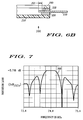
- FIG. 7 is a diagram of a measured SAW filter transfer function from a SAW device mounted in accordance with the present invention.
- FIG. 1 illustrates a bottom view of the
package base 10, showing thick-film interconnection pads 20 and through-platedvias 25. - Fig. 2 depicts a top view of the
package base 10, with thick-film conductors conductors vias 25 to effect electrical connection to theinterconnection pads 20 on the lower surface of thepackage base 10. - Fig. 3 illustrates a side view of the
package base 10 with a thermoplastic die attachmaterial 60 and a frequency selection component die, for example a surface acoustic wave (SAW) die 70, attached thereto. The thermoplastic die attachment adhesive 60 may be any of several such materials, depending on the melting point desired for a particular application. Table 1 provides several illustrative examples of thermoplasticdie attachment materials 60 together with the temperatures needed for forming bonds with these examples.TABLE 1 BONDING TEMPERATURES FOR SEVERAL THERMOPLASTIC MATERIALS MATERIAL BONDING TEMPERATURE(°C) Polyetheretherketone 360 Polysulfone 300-380 Polyethersulfone 320-380 Polyetherimide 340-380 Polybutlyeneterepthalate 240 Polycarbonate 230-290 - Fig. 4A shows a top view of a SAW device die 70, with
bond pad areas bond pad areas wire bonds 27 to portions ofconductor regions conductor regions material 60 beneath the SAW die 70 and which are also not located where the low-melting-temperature glass 110 attaches thelid 100 to thepackage base 10 as shown in Fig. 5A. The portions ofconductor regions material 60 serve as die attach pads, however, die attach pads are not necessary to this concept for die attachment. - One example of a low-melting-
temperature glass 110 is a mixture of PbO and V₂O₅. This can be used with a two minute bake at 3600° C to seal thelid 100 to thepackage base 10. - Fig. 5A provides a plan view of the bottom of the
ceramic lid 100, with thecentral region 105 hollowed out, as is shown in Fig.5B. - Fig. 5B is a cross-sectional view along line A-A in Fig. 5A of the
ceramic lid 100 and low-melting-temperature glass 110. - Fig. 6A depicts a plan view of an alternative embodiment of the
package 200. In this embodiment, thepackage base 200 is shown in Fig 6B to be composed of a layer ofceramic material 210, which has gold-plated Kovar leads 230 in a gold-platedKovar lead frame 240 sealed to theceramic material 210 by fusedglass 220. The glass-free area 201 of the gold-platedKovar lead 230 inside thepackage base 200 is used for bonding ofinterconnection wires 27 from thebond pads - As shown in Fig. 6B, the SAW die 70 is attached to the die
bonding pad 250 by means of a thermoplastic die attachmaterial 60 and electrical connection to the SAW die 70 is made by means of wire-bonds 27 as described and illustrated previously in Fig. 4B. Subsequent to the wirebonding operation, asolder preform 260 is placed on top of theupper metallized ring 240. Alid 270 is placed on top of thesolder preform 260 and thelid 270 is soldered to theupper metallization 240, hermetically sealing thelid 270 to thepackage base 200. - An example of a measured SAW
transmission frequency response 300 from a SAW device mounted in accordance with the present invention is provided in Fig. 7. The data shown in Fig. 7 illustrate that thedevice response 300 is in accordance with the SAW device design, showing that the packaging steps in accordance with the present invention does not inhibit the operation of theSAW device 70. - A
package 200 for a microelectronic device such as a circuit surfaceacoustic wave device 70 or a semiconductor circuit die in accordance with one embodiment of the invention is suitable for enclosing theSAW device 70 in a hermetically sealed environment such that the resultingstructure 200 takes up a minimum volume of space. Thepackage 200 may include adie pad 250 for the surface acoustic wave die 70 and does include athermoplastic adhesive 60 for affixing the SAW die 70 to thepackage base 210 without causing the top surface of the SAW die 70 to be in excessive compression or tension, either of which causes device malfunction. The thermoplastic die attach adhesive 60 allows theSAW device 70 to be exposed to greater temperatures than prior art enabled without suffering SAW die 70 contamination from outgassing of the die attach adhesive 60. This in turn allows thecover 270 to be affixed to thepackage base 200 by means ofsolder 260 to hermetically seal the SAW die 70 from the surrounding environment. Thebase 210, thermoplastic die attach adhesive 60,cover 270, and cover attachsolder 260 cooperate to provide a package which encloses and protects the SAW die 70. - While the invention has been described in conjunction with specific embodiments thereof, it is evident that many alterations, modifications and variations will be apparent to those skilled in the art in light of the foregoing description. Accordingly, the invention is intended to embrace all such alterations, modifications and variations in the appended claims.
Claims (10)
- A method for packaging of frequency selection component die (70) comprising the steps of:
forming a package base (10);
disposing conductors (30, 35, 40, 45, 50, 55) thereon;
disposing thermoplastic die attachment material (60) on the package base (10);
placing the frequency selection component die (70) on the thermoplastic die attachment material (60);
heating the package base (10), thermoplastic die attachment material (60), and frequency selection component die (70) to a temperature above the melting point of the thermoplastic die attachment material (60);
forming a bond between the frequency selection component die (70) and the package base (10);
forming electrical interconnections (27) from the frequency selection component die (70) to the package base conductors (30, 35, 40, 45, 50, 55); and
hermetically sealing a lid (100) to the package base (10). - The method for packaging of a frequency selection component die (70) as claimed in claim 1, wherein said step of forming electrical interconnections from the frequency selection component die (70) to the package base conductors (30, 35, 40, 45, 50, 55) includes the step of wirebonding (27) from the frequency selection component die (70) to the package base conductors (30, 35, 40, 45, 50, 55).
- The method for packaging of a frequency selection component die (70) as claimed in claim 1, wherein said step of hermetically sealing a lid (270) to the package base (10) includes the step of soldering a lid (270) to the package base (10) to form a hermetic seal.
- The method for packaging a frequency selection component die (70) as in claim 4, wherein said step of placing the frequency selection component die (70) on the thermoplastic die attachment material (60) includes the step of placing a surface acoustic wave device (70) on the thermoplastic die attachment material (60).
- The method for packaging of a frequency selection component die (70) as claimed in claim 1, wherein said step of forming a bond between frequency selection component die (70) and package base (10) includes the step of removing an assembly of the package base (10), thermoplastic die attachment material (60), and frequency selection component die (70) from the heat source and allowing the assembly to cool.
- The method for packaging a frequency selection component die (70) as claimed in claim 1, wherein said step of hermetically sealing a lid (100) to the package base (10) includes the steps of:
applying a low-firing-temperature glass (110) to the package base (10);
placing a lid (100) on the low-firing-temperature glass (110);
heating the low-firing-temperature glass (110), package base (10), and lid (100) to melt the low-firing-temperature glass (110); and
cooling the low-firing-temperature glass (110), package base (10), and lid (100) to form a hermetically sealed packaged frequency selection component die assembly. - The method for packaging a frequency selection component die (70) as claimed in claim 7, wherein said step of placing the lid (100) on the low-firing-temperature glass (110) includes the step of placing a ceramic lid (100) on the low-firing-temperature glass (110).
- The method for packaging a frequency selection component die (70) as claimed in claim 7, wherein said step of placing the lid (100) on the low-firing-temperature glass (110) includes the step of placing a glass lid (100) on the low-firing-temperature glass (110).
- A frequency selection component device assembly including in combination:
package base (10) means having a top surface;
conductor means (30, 35, 40, 45, 50, 55) disposed on said top surface;
thermoplastic die attachment means (60) disposed on said package base means (10) for bonding to said package base means (10);
frequency selection device means (70) bonded to said thermoplastic die attachment means (60);
said frequency selection device means (70) including interconnect pad means disposed on said frequency selection device means (70);
electrical interconnection means (27) attached to said interconnect pad means and to said electrical interconnect means for electrically connecting said frequency selection device means (70) to said conductor means (30, 35, 40, 45, 50, 55); and
means for providing a hermetic seal of said frequency selection component (70), said means for providing disposed on said package base (10) means. - The assembly claimed in claim 9 wherein said means for providing includes in combination:
solder means (260) disposed on said package base (10) means; and
cap means (270) disposed on said package base (10) means and soldered to said solder means 260 for forming a hermetic seal to said package base means (10).
Applications Claiming Priority (2)
| Application Number | Priority Date | Filing Date | Title |
|---|---|---|---|
| US65011791A | 1991-02-04 | 1991-02-04 | |
| US650117 | 1991-02-04 |
Publications (2)
| Publication Number | Publication Date |
|---|---|
| EP0498198A1 true EP0498198A1 (en) | 1992-08-12 |
| EP0498198B1 EP0498198B1 (en) | 1995-11-22 |
Family
ID=24607534
Family Applications (1)
| Application Number | Title | Priority Date | Filing Date |
|---|---|---|---|
| EP92100829A Expired - Lifetime EP0498198B1 (en) | 1991-02-04 | 1992-01-20 | Hermetic device package for microelectronic frequency selection components |
Country Status (4)
| Country | Link |
|---|---|
| US (1) | US5303457A (en) |
| EP (1) | EP0498198B1 (en) |
| JP (1) | JP3222525B2 (en) |
| DE (1) | DE69206165T2 (en) |
Cited By (1)
| Publication number | Priority date | Publication date | Assignee | Title |
|---|---|---|---|---|
| EP2043261A3 (en) * | 2007-09-27 | 2012-10-17 | Nihon Dempa Kogyo Co., Ltd. | Piezoelectric devices and methods for manufacturing same |
Families Citing this family (34)
| Publication number | Priority date | Publication date | Assignee | Title |
|---|---|---|---|---|
| US5420472A (en) * | 1992-06-11 | 1995-05-30 | Motorola, Inc. | Method and apparatus for thermal coefficient of expansion matched substrate attachment |
| JP3306272B2 (en) * | 1995-10-20 | 2002-07-24 | 富士通株式会社 | Surface acoustic wave device |
| EP0872495B1 (en) * | 1995-12-28 | 2001-11-14 | Daikin Industries, Limited | Fluorine-containing elastic copolymers, curable composition containing the same and sealant made therefrom |
| US6119920A (en) * | 1996-12-20 | 2000-09-19 | Rf Monolithics, Inc. | Method of forming an electronic package with a solder seal |
| US5892417A (en) * | 1996-12-27 | 1999-04-06 | Motorola Inc. | Saw device package and method |
| US6146743A (en) * | 1997-02-21 | 2000-11-14 | Medtronic, Inc. | Barrier metallization in ceramic substrate for implantable medical devices |
| US5855995A (en) * | 1997-02-21 | 1999-01-05 | Medtronic, Inc. | Ceramic substrate for implantable medical devices |
| US6303992B1 (en) | 1999-07-06 | 2001-10-16 | Visteon Global Technologies, Inc. | Interposer for mounting semiconductor dice on substrates |
| US6339276B1 (en) * | 1999-11-01 | 2002-01-15 | Agere Systems Guardian Corp. | Incremental tuning process for electrical resonators based on mechanical motion |
| US6323744B1 (en) | 2000-02-04 | 2001-11-27 | Agere Systems Guardian Corp. | Grounding of TFR ladder filters |
| US6437667B1 (en) | 2000-02-04 | 2002-08-20 | Agere Systems Guardian Corp. | Method of tuning thin film resonator filters by removing or adding piezoelectric material |
| US7296329B1 (en) | 2000-02-04 | 2007-11-20 | Agere Systems Inc. | Method of isolation for acoustic resonator device |
| US6377136B1 (en) | 2000-02-04 | 2002-04-23 | Agere Systems Guardian Corporation | Thin film resonator filter having at least one component with different resonant frequency sets or electrode capacitance |
| US6603241B1 (en) | 2000-05-23 | 2003-08-05 | Agere Systems, Inc. | Acoustic mirror materials for acoustic devices |
| US6355498B1 (en) | 2000-08-11 | 2002-03-12 | Agere Systems Guartian Corp. | Thin film resonators fabricated on membranes created by front side releasing |
| US6486751B1 (en) | 2000-09-26 | 2002-11-26 | Agere Systems Inc. | Increased bandwidth thin film resonator having a columnar structure |
| US6674291B1 (en) * | 2000-10-30 | 2004-01-06 | Agere Systems Guardian Corp. | Method and apparatus for determining and/or improving high power reliability in thin film resonator devices, and a thin film resonator device resultant therefrom |
| US6587212B1 (en) | 2000-10-31 | 2003-07-01 | Agere Systems Inc. | Method and apparatus for studying vibrational modes of an electro-acoustic device |
| US6743731B1 (en) * | 2000-11-17 | 2004-06-01 | Agere Systems Inc. | Method for making a radio frequency component and component produced thereby |
| US6550664B2 (en) * | 2000-12-09 | 2003-04-22 | Agilent Technologies, Inc. | Mounting film bulk acoustic resonators in microwave packages using flip chip bonding technology |
| US7651879B2 (en) * | 2005-12-07 | 2010-01-26 | Honeywell International Inc. | Surface acoustic wave pressure sensors |
| US8395247B1 (en) * | 2009-06-29 | 2013-03-12 | Integrated Device Technology, Inc. | Method and apparatus for placing quartz SAW devices together with clock/oscillator |
| DE102015102869B4 (en) * | 2015-02-27 | 2017-05-11 | Snaptrack, Inc. | High density integrated circuit MEMS device and method of making the same |
| EP3805201A4 (en) | 2018-05-28 | 2022-06-01 | Tokyo Institute of Technology | Nitrile oxide compound |
| US20210403622A1 (en) | 2018-11-02 | 2021-12-30 | Daikin Industries, Ltd. | Fluororubber composition and molded article |
| WO2020251056A1 (en) | 2019-06-14 | 2020-12-17 | ダイキン工業株式会社 | Compressed member for electrochemical device |
| JP7032676B2 (en) | 2019-11-05 | 2022-03-09 | ダイキン工業株式会社 | Laminates and extruded products |
| EP4215576A1 (en) | 2020-09-18 | 2023-07-26 | Daikin Industries, Ltd. | Composition for fluorine rubber crosslinking and molded article |
| WO2022210044A1 (en) | 2021-04-02 | 2022-10-06 | ダイキン工業株式会社 | Composition for fluorine rubber crosslinking and molded article |
| WO2022210041A1 (en) | 2021-04-02 | 2022-10-06 | ダイキン工業株式会社 | Composition for fluorine rubber crosslinking, molded product, and sealing material |
| CN117255829A (en) | 2021-04-02 | 2023-12-19 | 大金工业株式会社 | Composition for fluororubber crosslinking, molded article, and sealing material |
| CN117120537A (en) | 2021-04-15 | 2023-11-24 | 大金工业株式会社 | Composition for fluororubber crosslinking, molded article, and sealing material |
| CN117460781A (en) | 2021-06-15 | 2024-01-26 | 大金工业株式会社 | Composition for fluororubber crosslinking, molded article, and sealing material |
| JPWO2022264837A1 (en) | 2021-06-16 | 2022-12-22 |
Citations (1)
| Publication number | Priority date | Publication date | Assignee | Title |
|---|---|---|---|---|
| US4622433A (en) * | 1984-03-30 | 1986-11-11 | Diacon, Inc. | Ceramic package system using low temperature sealing glasses |
Family Cites Families (6)
| Publication number | Priority date | Publication date | Assignee | Title |
|---|---|---|---|---|
| JPS55127098A (en) * | 1979-03-09 | 1980-10-01 | Matsushita Electric Ind Co Ltd | Method of mounting electronic part |
| US4356047A (en) * | 1980-02-19 | 1982-10-26 | Consolidated Refining Co., Inc. | Method of making ceramic lid assembly for hermetic sealing of a semiconductor chip |
| US4592794A (en) * | 1981-09-01 | 1986-06-03 | Motorola, Inc. | Glass bonding method |
| US4459166A (en) * | 1982-03-08 | 1984-07-10 | Johnson Matthey Inc. | Method of bonding an electronic device to a ceramic substrate |
| US4550376A (en) * | 1983-02-14 | 1985-10-29 | Maciejczak Robert A | Inspection system for mechanical structures |
| US4906311A (en) * | 1985-09-24 | 1990-03-06 | John Fluke Co., Inc. | Method of making a hermetically sealed electronic component |
-
1992
- 1992-01-20 EP EP92100829A patent/EP0498198B1/en not_active Expired - Lifetime
- 1992-01-20 DE DE69206165T patent/DE69206165T2/en not_active Expired - Fee Related
- 1992-01-29 JP JP03858892A patent/JP3222525B2/en not_active Expired - Fee Related
- 1992-07-27 US US07/918,771 patent/US5303457A/en not_active Expired - Fee Related
Patent Citations (1)
| Publication number | Priority date | Publication date | Assignee | Title |
|---|---|---|---|---|
| US4622433A (en) * | 1984-03-30 | 1986-11-11 | Diacon, Inc. | Ceramic package system using low temperature sealing glasses |
Non-Patent Citations (3)
| Title |
|---|
| PATENT ABSTRACTS OF JAPAN vol. 01, no. 352 (E-458)27 November 1986 & JP-A-61 152 112 (HITACHI) 10 July 1986 * |
| PATENT ABSTRACTS OF JAPAN vol. 011, no. 244 (E-530)8 August 1987 & JP-A-62 054 931 (MITSUBISHI) 10 March 1987 * |
| PATENT ABSTRACTS OF JAPAN vol. 015, no. 054 (E-1031)8 February 1991 & JP-A-02 283 112 (MURATA) 20 November 1990 * |
Cited By (1)
| Publication number | Priority date | Publication date | Assignee | Title |
|---|---|---|---|---|
| EP2043261A3 (en) * | 2007-09-27 | 2012-10-17 | Nihon Dempa Kogyo Co., Ltd. | Piezoelectric devices and methods for manufacturing same |
Also Published As
| Publication number | Publication date |
|---|---|
| EP0498198B1 (en) | 1995-11-22 |
| US5303457A (en) | 1994-04-19 |
| DE69206165T2 (en) | 1996-06-05 |
| JP3222525B2 (en) | 2001-10-29 |
| DE69206165D1 (en) | 1996-01-04 |
| JPH0563482A (en) | 1993-03-12 |
Similar Documents
| Publication | Publication Date | Title |
|---|---|---|
| US5303457A (en) | Method for packaging microelectronic frequency selection components | |
| KR101460401B1 (en) | Module and method of manufacturing a module | |
| US6498422B1 (en) | Electronic component such as an saw device and method for producing the same | |
| KR100299415B1 (en) | How to mass seal and test electronic components at the same time and wafer level packaging | |
| JP2664754B2 (en) | High density electronic package and method of manufacturing the same | |
| US6114635A (en) | Chip-scale electronic component package | |
| US7816794B2 (en) | Electronic device and method of fabricating the same | |
| JP2009513026A (en) | Semiconductor structure and assembly method | |
| JP2002290200A (en) | Surface acoustic wave device and its manufacturing method | |
| JP2001053178A (en) | Electronic component with electronic circuit device sealed and mounted on circuit board, and manufacture of the electronic component | |
| US6928718B2 (en) | Method for array processing of surface acoustic wave devices | |
| US6182342B1 (en) | Method of encapsulating a saw device | |
| EP0098176A2 (en) | The packaging of semiconductor chips | |
| JPH1041420A (en) | High frequency device package | |
| CN114166198B (en) | Electronic device | |
| KR100473969B1 (en) | A method for manufacturing piezoelectric oscillation device, piezoelectric oscillation device, ceramic package and real time clock | |
| EP0241236A2 (en) | Cavity package for saw devices and associated electronics | |
| EP0525651B1 (en) | Package structure for one or more IC chips | |
| JPH0513603A (en) | Semiconductor integrated circuit device | |
| KR100431182B1 (en) | Surface acoustic wave device package and method | |
| US9166553B2 (en) | Surface acoustic wave (SAW) device package and method for fabricating same | |
| CN114166196B (en) | Method for manufacturing electronic device | |
| WO1998019349A1 (en) | An ultrasonically mounted piezoelectric device and method of making same | |
| KR100264644B1 (en) | Module package | |
| JPH0493059A (en) | Semiconductor package |
Legal Events
| Date | Code | Title | Description |
|---|---|---|---|
| PUAI | Public reference made under article 153(3) epc to a published international application that has entered the european phase |
Free format text: ORIGINAL CODE: 0009012 |
|
| AK | Designated contracting states |
Kind code of ref document: A1 Designated state(s): DE FR GB |
|
| 17P | Request for examination filed |
Effective date: 19930125 |
|
| 17Q | First examination report despatched |
Effective date: 19940826 |
|
| GRAA | (expected) grant |
Free format text: ORIGINAL CODE: 0009210 |
|
| AK | Designated contracting states |
Kind code of ref document: B1 Designated state(s): DE FR GB |
|
| REF | Corresponds to: |
Ref document number: 69206165 Country of ref document: DE Date of ref document: 19960104 |
|
| ET | Fr: translation filed | ||
| PLBE | No opposition filed within time limit |
Free format text: ORIGINAL CODE: 0009261 |
|
| STAA | Information on the status of an ep patent application or granted ep patent |
Free format text: STATUS: NO OPPOSITION FILED WITHIN TIME LIMIT |
|
| 26N | No opposition filed | ||
| PGFP | Annual fee paid to national office [announced via postgrant information from national office to epo] |
Ref country code: GB Payment date: 19981221 Year of fee payment: 8 |
|
| PGFP | Annual fee paid to national office [announced via postgrant information from national office to epo] |
Ref country code: FR Payment date: 19990107 Year of fee payment: 8 |
|
| PGFP | Annual fee paid to national office [announced via postgrant information from national office to epo] |
Ref country code: DE Payment date: 19990121 Year of fee payment: 8 |
|
| PG25 | Lapsed in a contracting state [announced via postgrant information from national office to epo] |
Ref country code: GB Free format text: LAPSE BECAUSE OF NON-PAYMENT OF DUE FEES Effective date: 20000120 |
|
| GBPC | Gb: european patent ceased through non-payment of renewal fee |
Effective date: 20000120 |
|
| PG25 | Lapsed in a contracting state [announced via postgrant information from national office to epo] |
Ref country code: FR Free format text: LAPSE BECAUSE OF NON-PAYMENT OF DUE FEES Effective date: 20000929 |
|
| PG25 | Lapsed in a contracting state [announced via postgrant information from national office to epo] |
Ref country code: DE Free format text: LAPSE BECAUSE OF NON-PAYMENT OF DUE FEES Effective date: 20001101 |
|
| REG | Reference to a national code |
Ref country code: FR Ref legal event code: ST |