EP0498651A2 - High power factor power supply - Google Patents
High power factor power supply Download PDFInfo
- Publication number
- EP0498651A2 EP0498651A2 EP92301011A EP92301011A EP0498651A2 EP 0498651 A2 EP0498651 A2 EP 0498651A2 EP 92301011 A EP92301011 A EP 92301011A EP 92301011 A EP92301011 A EP 92301011A EP 0498651 A2 EP0498651 A2 EP 0498651A2
- Authority
- EP
- European Patent Office
- Prior art keywords
- converter
- coupled
- output
- power supply
- voltage
- Prior art date
- Legal status (The legal status is an assumption and is not a legal conclusion. Google has not performed a legal analysis and makes no representation as to the accuracy of the status listed.)
- Granted
Links
Images

Classifications
-
- H—ELECTRICITY
- H02—GENERATION; CONVERSION OR DISTRIBUTION OF ELECTRIC POWER
- H02M—APPARATUS FOR CONVERSION BETWEEN AC AND AC, BETWEEN AC AND DC, OR BETWEEN DC AND DC, AND FOR USE WITH MAINS OR SIMILAR POWER SUPPLY SYSTEMS; CONVERSION OF DC OR AC INPUT POWER INTO SURGE OUTPUT POWER; CONTROL OR REGULATION THEREOF
- H02M1/00—Details of apparatus for conversion
- H02M1/42—Circuits or arrangements for compensating for or adjusting power factor in converters or inverters
- H02M1/4208—Arrangements for improving power factor of AC input
-
- H—ELECTRICITY
- H02—GENERATION; CONVERSION OR DISTRIBUTION OF ELECTRIC POWER
- H02M—APPARATUS FOR CONVERSION BETWEEN AC AND AC, BETWEEN AC AND DC, OR BETWEEN DC AND DC, AND FOR USE WITH MAINS OR SIMILAR POWER SUPPLY SYSTEMS; CONVERSION OF DC OR AC INPUT POWER INTO SURGE OUTPUT POWER; CONTROL OR REGULATION THEREOF
- H02M7/00—Conversion of ac power input into dc power output; Conversion of dc power input into ac power output
-
- H—ELECTRICITY
- H02—GENERATION; CONVERSION OR DISTRIBUTION OF ELECTRIC POWER
- H02M—APPARATUS FOR CONVERSION BETWEEN AC AND AC, BETWEEN AC AND DC, OR BETWEEN DC AND DC, AND FOR USE WITH MAINS OR SIMILAR POWER SUPPLY SYSTEMS; CONVERSION OF DC OR AC INPUT POWER INTO SURGE OUTPUT POWER; CONTROL OR REGULATION THEREOF
- H02M3/00—Conversion of dc power input into dc power output
- H02M3/22—Conversion of dc power input into dc power output with intermediate conversion into ac
- H02M3/24—Conversion of dc power input into dc power output with intermediate conversion into ac by static converters
- H02M3/28—Conversion of dc power input into dc power output with intermediate conversion into ac by static converters using discharge tubes with control electrode or semiconductor devices with control electrode to produce the intermediate ac
- H02M3/325—Conversion of dc power input into dc power output with intermediate conversion into ac by static converters using discharge tubes with control electrode or semiconductor devices with control electrode to produce the intermediate ac using devices of a triode or a transistor type requiring continuous application of a control signal
- H02M3/335—Conversion of dc power input into dc power output with intermediate conversion into ac by static converters using discharge tubes with control electrode or semiconductor devices with control electrode to produce the intermediate ac using devices of a triode or a transistor type requiring continuous application of a control signal using semiconductor devices only
- H02M3/337—Conversion of dc power input into dc power output with intermediate conversion into ac by static converters using discharge tubes with control electrode or semiconductor devices with control electrode to produce the intermediate ac using devices of a triode or a transistor type requiring continuous application of a control signal using semiconductor devices only in push-pull configuration
- H02M3/3376—Conversion of dc power input into dc power output with intermediate conversion into ac by static converters using discharge tubes with control electrode or semiconductor devices with control electrode to produce the intermediate ac using devices of a triode or a transistor type requiring continuous application of a control signal using semiconductor devices only in push-pull configuration with automatic control of output voltage or current
-
- H—ELECTRICITY
- H02—GENERATION; CONVERSION OR DISTRIBUTION OF ELECTRIC POWER
- H02M—APPARATUS FOR CONVERSION BETWEEN AC AND AC, BETWEEN AC AND DC, OR BETWEEN DC AND DC, AND FOR USE WITH MAINS OR SIMILAR POWER SUPPLY SYSTEMS; CONVERSION OF DC OR AC INPUT POWER INTO SURGE OUTPUT POWER; CONTROL OR REGULATION THEREOF
- H02M1/00—Details of apparatus for conversion
- H02M1/42—Circuits or arrangements for compensating for or adjusting power factor in converters or inverters
- H02M1/4208—Arrangements for improving power factor of AC input
- H02M1/4275—Arrangements for improving power factor of AC input by adding an auxiliary output voltage in series to the input
-
- Y—GENERAL TAGGING OF NEW TECHNOLOGICAL DEVELOPMENTS; GENERAL TAGGING OF CROSS-SECTIONAL TECHNOLOGIES SPANNING OVER SEVERAL SECTIONS OF THE IPC; TECHNICAL SUBJECTS COVERED BY FORMER USPC CROSS-REFERENCE ART COLLECTIONS [XRACs] AND DIGESTS
- Y02—TECHNOLOGIES OR APPLICATIONS FOR MITIGATION OR ADAPTATION AGAINST CLIMATE CHANGE
- Y02B—CLIMATE CHANGE MITIGATION TECHNOLOGIES RELATED TO BUILDINGS, e.g. HOUSING, HOUSE APPLIANCES OR RELATED END-USER APPLICATIONS
- Y02B70/00—Technologies for an efficient end-user side electric power management and consumption
- Y02B70/10—Technologies improving the efficiency by using switched-mode power supplies [SMPS], i.e. efficient power electronics conversion e.g. power factor correction or reduction of losses in power supplies or efficient standby modes
-
- Y—GENERAL TAGGING OF NEW TECHNOLOGICAL DEVELOPMENTS; GENERAL TAGGING OF CROSS-SECTIONAL TECHNOLOGIES SPANNING OVER SEVERAL SECTIONS OF THE IPC; TECHNICAL SUBJECTS COVERED BY FORMER USPC CROSS-REFERENCE ART COLLECTIONS [XRACs] AND DIGESTS
- Y02—TECHNOLOGIES OR APPLICATIONS FOR MITIGATION OR ADAPTATION AGAINST CLIMATE CHANGE
- Y02P—CLIMATE CHANGE MITIGATION TECHNOLOGIES IN THE PRODUCTION OR PROCESSING OF GOODS
- Y02P80/00—Climate change mitigation technologies for sector-wide applications
- Y02P80/10—Efficient use of energy, e.g. using compressed air or pressurized fluid as energy carrier
Definitions
- the present invention relates generally to power supplies and, more particularly, to a power supply including an ac-to-dc switching converter operating with high input power factor while maintaining fast transient response at its output.
- a power conversion system employing a single power stage while operating at high power factor is described in commonly assigned U.S. Pat. No. 4,642,745 issued on February 10, 1987 to R.L. Steigerwald and W.P. Kornrumpf, which patent is incorporated by reference herein.
- the power conversion system of the Steigerwald and Kornrumpf patent includes: a full-wave ac rectifier; a dc-to-ac converter; a transformer having a primary winding, a closely-coupled secondary output winding and a loosely-coupled secondary boost winding; and a resonant capacitor coupled to the secondary boost winding.
- the secondary output winding is controlled by pulse width modulation (PWM), and the secondary boost winding is controlled by frequency modulation, thus allowing relatively independent control of the input current and output voltage.
- PWM pulse width modulation
- the secondary boost winding and the primary boost winding of the Steigerwald and Kornrumpf patent are coupled, albeit loosely, any adjustment in the dc output voltage by the PWM control affects the input current waveform. Therefore, although the power supply of the hereinabove cited Steigerwald and Kornrumpf patent results in relatively high power factor using only one power stage, it may be desirable in some applications to further increase power factor and otherwise improve performance (e.g., by lowering the output ripple current) by completely decoupling the boosting converter and the power supply output voltage.
- an object of the present invention is to provide a new and improved off-line switching power supply including a single power stage with two outputs operating at a high power factor.
- Another object of the present invention is to provide an off-line switching power supply, including a dual-output converter, capable of drawing high quality current waveforms from the ac source while producing a regulated dc output voltage with fast transient response.
- Still another object of the present invention is to provide an off-line switching power supply which includes a dual-output power converter having one output coupled in series with the input thereof in order to provide a high power factor and having the other output provide a dc voltage as the power supply output.
- Yet another object of the present invention is to provide a high power factor "front-end" power supply, e.g. suitable for supplying a dc bus in a distributed power system or to retrofit existing low power factor switching power supplies.
- an off-line switching power supply including an ac rectifier and a dual-output switching converter having a first output coupled between the ac rectifier and the input to the dual-output converter for providing a high power factor, the other, i.e. second, output providing a dc voltage as the power supply output.
- the outputs of the dual-output converter are fully decoupled so as to allow independent control of the ac input current and the power supply output voltage.
- a full-wave ac rectifier bridge is coupled in series with the first output of the dual-output power converter via an input boosting converter means.
- the boosting converter means includes the parallel combination of a boost transformer secondary winding and a resonant capacitance and further includes a boost rectifier.
- the output terminal of the boosting converter means is coupled to a dc link.
- a pair of series-connected energy-storage capacitors, having substantially the same capacitance, is connected between the dc link at the output of the boosting converter means and ground.
- a full-bridge dc-to-ac converter is also coupled between the dc link and ground for providing a first ac signal to excite the boosting converter means.
- a boost transformer primary winding is coupled in series with a resonant inductance, the series combination being coupled between the center tap joining the two energy-storage capacitors and one leg of the full-bridge converter.
- the full-bridge converter provides a second ac voltage through a transformer to an output rectifier to generate a regulated dc output voltage.
- the two outputs of the dual-output converter are independently controlled.
- PWM means are provided to control the amplitude of the regulated output voltage (i.e., the second output), while active frequency control of the boosting converter means is provided to control the first output voltage by controlling the amplitude of the ac input current.
- such frequency control of the boosting converter means is passive, i.e., depends on the gain characteristics of the boosting converter resonant circuit.
- the off-line switching power supply of the present invention is capable of drawing high quality current waveforms from the ac source while producing a regulated dc output voltage with fast transient response.
- a self-contained high power factor "front-end” power supply e.g. for supplying a dc bus in a distributed power system or to retrofit existing low power factor switching power supplies, is provided by the combination of an ac rectifier and a dc-to-ac converter, the output of the dc-to-ac converter being coupled in series with the ac rectifier.
- the dc-to-ac converter comprises either a full-bridge or half-bridge converter, the output of which is coupled in series with the ac rectifier via a resonant boosting converter means.
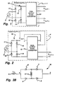
- Figure 1 illustrates a power supply 1 of a type well-known in the art for receiving an ac power line voltage from an ac power source 2 and providing two independently controllable output voltages E out1 and E out2 .
- the power supply 1 includes a full-wave rectifier 10, having diodes 11-14 connected together in a full-bridge configuration, for providing a rectified ac line voltage to a typical dual-output dc-to-dc converter 15.
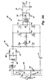
- Figure 3A illustrates one preferred embodiment of an off-line switching power supply according to the present invention for converting an ac power line voltage to a regulated dc output voltage.
- the power supply of the present invention includes full-wave rectifier 10, having diodes 11-14 connected together in a full-bridge configuration, coupled to ac power source 2.
- Rectifier 10 provides a full-wave rectified voltage between points b and o.
- a boosting converter output circuit 16 is coupled in series with the full-bridge rectifier via a high-frequency filter inductor L in .
- high-frequency filter inductor L in may be connected on the ac side of rectifier 10, if desired.
- the boosting converter output circuit 16 includes a center-tapped boost transformer secondary winding 18 of a boost transformer T b coupled in parallel with a resonant capacitor C r .
- the boosting converter output circuit further includes a center-tapped transformer, full-wave boost rectifier comprising diodes 20 and 21, the anodes of which diodes are connected to the respective terminals of the resonant capacitor C r .
- the cathodes of diodes 20 and 21 are connected together at a point a which is connected to the dc link at potential V ao .
- a dc-to-ac converter 22 comprising a full-bridge connection of switching devices Q1-Q4 is connected between the dc link and ground.
- the series combination of a boost transformer primary winding 24 and a resonant inductor L r is coupled between the junction joining switching devices Q1 and Q2 of converter 22 and the junction joining a center-tapped pair of relatively large energy-storage capacitors C in 2 .
- capacitors C in 2 may be relatively small if the series combination thereof is coupled in parallel with another energy-storage capacitor (not shown) which is relatively large.
- boosting converter output circuit 16 includes a full-wave bridge rectifier comprising diodes 6-9 and a single secondary winding 17 of boost transformer T b .
- boosting power converter output circuit 16 is shown in Figure 3A as comprising a parallel resonant circuit, it is to be understood that the advantages of the present invention may also be realized using other resonant circuit configurations.
- a combination series/parallel resonant circuit may be employed wherein another capacitor C r2 (not shown) is coupled in series with resonant inductor L r on either the primary or secondary side of transformer T b .
- a series resonant circuit configuration may be employed wherein resonant capacitor C r is situated in series with resonant inductor L r , on either the primary or secondary side of transformer T b , rather than in parallel therewith as shown in Figure 3A.
- the primary winding 26 of another transformer 27 is coupled across the junctions joining the switching devices Q1-Q2 and Q3-Q4 of the respective full-bridge converter legs.
- the respective terminals of the secondary winding 28 of transformer 27 are connected to the anodes of diodes 30 and 31.
- the cathodes of diodes 30 and 31 are connected to an output filter inductor 32 and an output filter capacitor 34.
- the regulated dc output voltage E out is provided across capacitor 34.
- the boosting converter provides the instantaneous voltage difference between the output voltage
- the output voltage of the resonant boosting converter is controlled by the switching frequency of full-bridge converter switching devices Q1-Q4 via a first ac signal generated across the boosting converter resonant circuit L r and C r , while the dc output voltage E out is controlled by pulse width modulation (PWM) of a second ac signal generated across transformer 27, i.e. by phase-shifting the two legs of the converter bridge with respect to each other.
- PWM pulse width modulation
- the boosting converter voltage V ab is independent of the power supply output voltage E out .
- a fast transient response is attained for the input boosting converter and the power supply output voltage simultaneously.
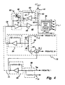
- a suitable control for the power supply of the present invention is illustrated in Figure 4 and described in Steigerwald and Kornrumpf U.S. Pat. No. 4,642,745, cited hereinabove.
- the reference numbers in Figure 4 correspond to those in the Steigerwald and Kornrumpf patent.
- the Steigerwald and Kornrumpf patent describes a PWM control for controlling the regulated dc output voltage by adjusting the duty cycle of the inverter output signal whenever an error is detected between the commanded dc output voltage E out * and the actual dc output voltage E out .
- the Steigerwald and Kornrumpf patent describes an active frequency control wherein the actual converter input current is compared with a commanded current in phase with the utility line voltage; any difference causes a frequency adjustment for controlling a boosting converter.
- the boosting converter and the power supply output voltage of the present invention are completely decoupled, any adjustment of the dc output voltage using the Steigerwald and Kornrumpf control system will have no effect on the input current to the converter of the present invention.
- the power supply of the present invention operates with a relatively high power factor and low peak ac line current, due to the favorable gain characteristics of the parallel resonant circuit L r and C r .
- the resonant circuit is lightly loaded so that the boosting converter output voltage can ring up to provide the high boost needed, i.e., the difference between the low value of the instantaneous ac line voltage
- the boosting converter output voltage can ring up to provide the high boost needed, i.e., the difference between the low value of the instantaneous ac line voltage
- the resonant circuit is highly damped.
- the power supply of the present invention does not require active control of the input ac current waveform in order to provide a high power factor.
- the portion of the control 40 in Figure 4 represented by dashed lines 70 can thus advantageously be eliminated, with the output of compensator gain block 69 being coupled to the input of ramp generator 58 (as shown by the dashed line 71) via resistor 58, if desired, thereby simplifying the controls required for the high power factor power supply of the present invention.
- the boosting power converter is not required to convert the entire power delivered to the load. That is, for a dc link voltage V ao which is not substantially greater than the peak of the ac input voltage, i.e. less than twice the peak of the ac input voltage, the peak rating of the boosting power converter is less than the peak power delivered to the dc link, as a result of the series connection of the boosting converter in the switching power supply. For example, for a dc link voltage V ao of approximately 25% above the peak of the ac line voltage, the peak power converted by the boosting converter is approximately 78% of the full power delivered, and the average power processed by the boosting converter is approximately 59% of the full power delivered.
- Figure 5 illustrates another aspect of the power supply of the present invention that is especially suitable for applications wherein a self-contained ac-to-dc "front-end" converter is desirable, e.g. to supply a dc bus in a distributed power system or to retrofit existing low power factor switching power supplies.
- a self-contained ac-to-dc "front-end" converter is desirable, e.g. to supply a dc bus in a distributed power system or to retrofit existing low power factor switching power supplies.
- the center-tapped energy-storage capacitors C in 2 of Figure 3A have been replaced by a single equivalent energy-storage capacitor C in , and a dedicated resonant half-bridge converter 80 has been coupled thereacross.
- Converter 80 includes the series combination of switching devices Q1 and Q2 with the resonant circuit comprising the series combination of boost primary winding 24, resonant inductance L r , and capacitance C b (or, alternatively, a pair of capacitors C b 2 coupled in parallel as shown in Figure 3A for capacitors C in 2 ) at the junction between switching devices Q1 and Q2.
- the resonant boosting converter of Figure 5 may be controlled by the switching frequency of half-bridge converter switching devices Q1 and Q2, a suitable frequency control being described in the Steigerwald and Kornrumpf patent, U.S. Pat. No. 4,642,745, cited hereinabove.
- the resonant boosting converter could be controlled by suitable PWM control.
Abstract
Description
- The present invention relates generally to power supplies and, more particularly, to a power supply including an ac-to-dc switching converter operating with high input power factor while maintaining fast transient response at its output.
- Conventional rectifiers have relatively low power factors which limit the power that can be drawn from an ac line to a fraction of the rating of the line. Furthermore, highly distorted ac line currents are drawn by these conventional rectifiers, often causing interference with other electrical equipment in addition to equipment overcurrents and overvoltages. Techniques for improving power factor include passive waveform shaping methods, i.e. using input filters, and active methods, i.e. using boost or buck converter topologies. Such conventional active methods of obtaining high power factor generally employ a completely separate up-front converter to attain the high power factor followed by a dc-to-dc converter to produce the desired regulated dc output voltage. Thus, the power is converted twice, which is costly and inefficient. Moreover, the up-front converter must convert the entire delivered power. In fact, it must convert a peak power equal to twice the average power delivered.
- A power conversion system employing a single power stage while operating at high power factor is described in commonly assigned U.S. Pat. No. 4,642,745 issued on February 10, 1987 to R.L. Steigerwald and W.P. Kornrumpf, which patent is incorporated by reference herein. The power conversion system of the Steigerwald and Kornrumpf patent includes: a full-wave ac rectifier; a dc-to-ac converter; a transformer having a primary winding, a closely-coupled secondary output winding and a loosely-coupled secondary boost winding; and a resonant capacitor coupled to the secondary boost winding. The secondary output winding is controlled by pulse width modulation (PWM), and the secondary boost winding is controlled by frequency modulation, thus allowing relatively independent control of the input current and output voltage. However, since the secondary boost winding and the primary boost winding of the Steigerwald and Kornrumpf patent are coupled, albeit loosely, any adjustment in the dc output voltage by the PWM control affects the input current waveform. Therefore, although the power supply of the hereinabove cited Steigerwald and Kornrumpf patent results in relatively high power factor using only one power stage, it may be desirable in some applications to further increase power factor and otherwise improve performance (e.g., by lowering the output ripple current) by completely decoupling the boosting converter and the power supply output voltage.
- Accordingly, an object of the present invention is to provide a new and improved off-line switching power supply including a single power stage with two outputs operating at a high power factor.
- Another object of the present invention is to provide an off-line switching power supply, including a dual-output converter, capable of drawing high quality current waveforms from the ac source while producing a regulated dc output voltage with fast transient response.
- Still another object of the present invention is to provide an off-line switching power supply which includes a dual-output power converter having one output coupled in series with the input thereof in order to provide a high power factor and having the other output provide a dc voltage as the power supply output.
- Yet another object of the present invention is to provide a high power factor "front-end" power supply, e.g. suitable for supplying a dc bus in a distributed power system or to retrofit existing low power factor switching power supplies.
- The foregoing and other objects of the present invention are achieved in an off-line switching power supply including an ac rectifier and a dual-output switching converter having a first output coupled between the ac rectifier and the input to the dual-output converter for providing a high power factor, the other, i.e. second, output providing a dc voltage as the power supply output. The outputs of the dual-output converter are fully decoupled so as to allow independent control of the ac input current and the power supply output voltage.
- In a preferred embodiment, a full-wave ac rectifier bridge is coupled in series with the first output of the dual-output power converter via an input boosting converter means. The boosting converter means includes the parallel combination of a boost transformer secondary winding and a resonant capacitance and further includes a boost rectifier. The output terminal of the boosting converter means is coupled to a dc link. A pair of series-connected energy-storage capacitors, having substantially the same capacitance, is connected between the dc link at the output of the boosting converter means and ground. A full-bridge dc-to-ac converter is also coupled between the dc link and ground for providing a first ac signal to excite the boosting converter means. A boost transformer primary winding is coupled in series with a resonant inductance, the series combination being coupled between the center tap joining the two energy-storage capacitors and one leg of the full-bridge converter. The full-bridge converter provides a second ac voltage through a transformer to an output rectifier to generate a regulated dc output voltage. The two outputs of the dual-output converter are independently controlled. For example, in a preferred embodiment, PWM means are provided to control the amplitude of the regulated output voltage (i.e., the second output), while active frequency control of the boosting converter means is provided to control the first output voltage by controlling the amplitude of the ac input current. In another preferred embodiment, such frequency control of the boosting converter means is passive, i.e., depends on the gain characteristics of the boosting converter resonant circuit. As a result of the complete decoupling of the input boosting converter means and the power supply output voltage, the off-line switching power supply of the present invention is capable of drawing high quality current waveforms from the ac source while producing a regulated dc output voltage with fast transient response.
- In another aspect of the present invention, a self-contained high power factor "front-end" power supply, e.g. for supplying a dc bus in a distributed power system or to retrofit existing low power factor switching power supplies, is provided by the combination of an ac rectifier and a dc-to-ac converter, the output of the dc-to-ac converter being coupled in series with the ac rectifier. In a preferred embodiment, the dc-to-ac converter comprises either a full-bridge or half-bridge converter, the output of which is coupled in series with the ac rectifier via a resonant boosting converter means. As a result, high quality current waveforms are drawn from the ac source and a high power factor dc output voltage is provided for supplying the system load, e.g. a plurality of dc-to-dc converters in a distributed power system.
- The features and advantages of the present invention will become apparent from the following detailed description of the invention when read with the accompanying drawings in which:
- Figure 1 is a schematic illustration of a typical dual-output power supply;
- Figure 2 is a schematic illustration of a power supply including a dual-output dc-to-dc converter in accordance with the present invention;
- Figure 3A is a schematic illustration of a preferred embodiment of an off-line switching power supply of the present invention;
- Figure 3B is a schematic illustration of an alternative embodiment of a boosting converter output circuit useful in the off-line switching power supply of the present invention;
- Figure 4 is a schematic illustration of a suitable control system for controlling operation of the power supply of the present invention; and
- Figure 5 is a schematic illustration of an alternative embodiment of an off-line switching power supply according to the present invention.
- Figure 1 illustrates a
power supply 1 of a type well-known in the art for receiving an ac power line voltage from anac power source 2 and providing two independently controllable output voltages Eout1 and Eout2. Thepower supply 1 includes a full-wave rectifier 10, having diodes 11-14 connected together in a full-bridge configuration, for providing a rectified ac line voltage to a typical dual-output dc-to-dc converter 15. - In accordance with the present invention, as shown in Figure 2, by coupling one of the outputs, e.g. Eout1, of dual-
output converter 15 in series with the rectified ac line voltage, a high powerfactor power supply 4 for providing a dc output voltage Eout2 is realized. - Figure 3A illustrates one preferred embodiment of an off-line switching power supply according to the present invention for converting an ac power line voltage to a regulated dc output voltage. According to the embodiment of Figure 3A, the power supply of the present invention includes full-
wave rectifier 10, having diodes 11-14 connected together in a full-bridge configuration, coupled toac power source 2.Rectifier 10 provides a full-wave rectified voltage between points b and o. As shown in Figure 3A, a boostingconverter output circuit 16 is coupled in series with the full-bridge rectifier via a high-frequency filter inductor Lin. Alternatively, high-frequency filter inductor Lin may be connected on the ac side ofrectifier 10, if desired. The boostingconverter output circuit 16 includes a center-tapped boost transformersecondary winding 18 of a boost transformer Tb coupled in parallel with a resonant capacitor Cr. The boosting converter output circuit further includes a center-tapped transformer, full-wave boostrectifier comprising diodes diodes - As shown in Figure 3A, a dc-to-
ac converter 22 comprising a full-bridge connection of switching devices Q₁-Q₄ is connected between the dc link and ground. The series combination of a boost transformerprimary winding 24 and a resonant inductor Lr is coupled between the junction joining switching devices Q₁ and Q₂ ofconverter 22 and the junction joining a center-tapped pair of relatively large energy-storage capacitors

- An alternative embodiment of boosting
converter output circuit 16, as shown in Figure 3B, includes a full-wave bridge rectifier comprising diodes 6-9 and a single secondary winding 17 of boost transformer Tb. Furthermore, although boosting powerconverter output circuit 16 is shown in Figure 3A as comprising a parallel resonant circuit, it is to be understood that the advantages of the present invention may also be realized using other resonant circuit configurations. For example, a combination series/parallel resonant circuit may be employed wherein another capacitor Cr2 (not shown) is coupled in series with resonant inductor Lr on either the primary or secondary side of transformer Tb. As another example, a series resonant circuit configuration may be employed wherein resonant capacitor Cr is situated in series with resonant inductor Lr , on either the primary or secondary side of transformer Tb, rather than in parallel therewith as shown in Figure 3A. - The
primary winding 26 of anothertransformer 27 is coupled across the junctions joining the switching devices Q₁-Q₂ and Q₃-Q₄ of the respective full-bridge converter legs. The respective terminals of thesecondary winding 28 oftransformer 27 are connected to the anodes ofdiodes diodes output filter inductor 32 and anoutput filter capacitor 34. The regulated dc output voltage Eout is provided acrosscapacitor 34. - In operation, the boosting converter provides the instantaneous voltage difference between the output voltage |vL| of the full-
bridge rectifier 10 and the dc link voltage Vao. The output voltage of the resonant boosting converter is controlled by the switching frequency of full-bridge converter switching devices Q₁-Q₄ via a first ac signal generated across the boosting converter resonant circuit Lr and Cr, while the dc output voltage Eout is controlled by pulse width modulation (PWM) of a second ac signal generated acrosstransformer 27, i.e. by phase-shifting the two legs of the converter bridge with respect to each other. Because phase-shifting the two full-bridge converter legs does not affect the voltage applied to the resonant circuit Lr and Cr, the boosting converter voltage Vab is independent of the power supply output voltage Eout. As a result, a fast transient response is attained for the input boosting converter and the power supply output voltage simultaneously. - A suitable control for the power supply of the present invention is illustrated in Figure 4 and described in Steigerwald and Kornrumpf U.S. Pat. No. 4,642,745, cited hereinabove. (The reference numbers in Figure 4 correspond to those in the Steigerwald and Kornrumpf patent.) The Steigerwald and Kornrumpf patent describes a PWM control for controlling the regulated dc output voltage by adjusting the duty cycle of the inverter output signal whenever an error is detected between the commanded dc output voltage E

- As another advantage, it has been found that even with no active control of the ac line current, the power supply of the present invention operates with a relatively high power factor and low peak ac line current, due to the favorable gain characteristics of the parallel resonant circuit Lr and Cr. Near the valleys of the input ac current waveform, low power is delivered, and the resonant circuit is lightly loaded so that the boosting converter output voltage can ring up to provide the high boost needed, i.e., the difference between the low value of the instantaneous ac line voltage |vL| and the dc link voltage Vao. Conversely, near the peaks of the input ac current waveform, higher power is delivered and the resonant circuit is highly damped. As a result, little boosting action is needed. Hence, the gain characteristics of the parallel resonant boosting converter naturally cause the power supply to yield a high power factor. Advantageously, therefore, the power supply of the present invention does not require active control of the input ac current waveform in order to provide a high power factor. The portion of the
control 40 in Figure 4 represented by dashedlines 70 can thus advantageously be eliminated, with the output ofcompensator gain block 69 being coupled to the input of ramp generator 58 (as shown by the dashed line 71) viaresistor 58, if desired, thereby simplifying the controls required for the high power factor power supply of the present invention. - As still another advantage, the boosting power converter is not required to convert the entire power delivered to the load. That is, for a dc link voltage Vao which is not substantially greater than the peak of the ac input voltage, i.e. less than twice the peak of the ac input voltage, the peak rating of the boosting power converter is less than the peak power delivered to the dc link, as a result of the series connection of the boosting converter in the switching power supply. For example, for a dc link voltage Vao of approximately 25% above the peak of the ac line voltage, the peak power converted by the boosting converter is approximately 78% of the full power delivered, and the average power processed by the boosting converter is approximately 59% of the full power delivered.
- Figure 5 illustrates another aspect of the power supply of the present invention that is especially suitable for applications wherein a self-contained ac-to-dc "front-end" converter is desirable, e.g. to supply a dc bus in a distributed power system or to retrofit existing low power factor switching power supplies. As shown in Figure 5, the center-tapped energy-storage capacitors

capacitors 

- While the power converter of the present invention has been described with reference to power supplies including dual-output converters, the outputs of which are either resonant frequency controlled, PWM controlled, or a combination thereof, it is to be understood that any type of dual-output power converter can be used in a power supply in accordance with the present invention to achieve the advantages thereof. Hence, while the preferred embodiments of the present invention have been shown and described herein, it will be obvious that such embodiments are provided by way of example only. Numerous variations, changes and substitutions will occur to those of skill in the art without departing from the invention herein. Accordingly, it is intended that the invention be limited only by the spirit and scope of the appended claims.
Claims (18)
- A high power factor power supply for providing a dc output voltage, comprising:
ac rectifying means for providing a rectified ac voltage when coupled to an ac power line;
a dual-output power converter for providing first and second output voltages, said output voltages being independently controllable, said first output voltage being coupled in series between said ac rectifying means and the input of said dual-output power converter, and said first output voltage comprising the power supply dc output voltage. - A power supply, comprising:
ac rectifying means for providing a rectified ac voltage when coupled to an ac power line;
a dual-output converter including boosting converter means and dc-to-ac converter means, said boosting converter means including a boost transformer secondary winding coupled in series between said ac rectifying means and a dc link voltage, said boosting converter means further comprising resonant circuit means including a combination of the boost transformer, a resonant inductance and a resonant capacitance, said dc-to-ac converter means receiving said dc link voltage and generating first and second ac signals, said first ac signal exciting said boosting converter means, the amplitude of the input current to said boosting converter means being dependent on the frequency of said first ac signal;
output rectifier means for receiving said second ac signal and generating a regulated output dc voltage therefrom, said regulated output dc voltage being decoupled from the output voltage of said resonant circuit means; and
pulse width modulation means coupled to said output rectifier means for controlling the amplitude of said regulated output dc voltage by pulse width modulating said second ac signal. - The power supply of claim 2, further comprising frequency modulation means for controlling the frequency of said first ac signal in a manner to cause said power converter to draw a substantially sinusoidal current from said ac power line in phase with the voltage of said power line.
- The power supply of claim 2 wherein said boost transformer secondary winding includes a center tap, said center tap being coupled to said ac rectifying means; and said power converter further comprises a center-tapped full-wave boost rectifier coupled to said boost transformer secondary winding.
- The power supply of claim 2, further comprising a full-wave boost rectifier comprising a parallel combination of two pairs of series-connected diodes, said boost transformer secondary winding being coupled between the junctions joining the diodes of each respective pair.
- The power supply of claim 2 wherein said resonant capacitance is coupled in parallel with the boost transformer, and said resonant inductance is coupled in series with the boost transformer.
- The power supply of claim 2 wherein said resonant capacitance is coupled in series with said resonant inductance, the series combination of said resonant capacitance and said resonant inductance being coupled in series with the boost transformer.
- The power supply of claim 2 wherein;
said resonant capacitance is coupled in parallel with the boost transformer;
said resonant inductance is coupled in series with the boost transformer; and
said resonant circuit means further includes an additional resonant capacitance coupled in series with said resonant inductance. - The power supply of claim 2 wherein said dc-to-ac converter means comprises a full-bridge converter.
- A power supply, comprising:
ac rectifying means for providing a rectified ac voltage when coupled to an ac power line;
boosting converter means including a boost transformer secondary winding coupled in series between said ac rectifying means and a dc link voltage, said boosting converter means further comprising resonant circuit means including a combination of the boost transformer, a resonant inductance and a resonant capacitance;
dc-to-ac converter means for receiving said dc link voltage and generating an ac signal for exciting said boosting converter means, the amplitude of the input current to said boosting converter means being dependent on the frequency of said ac signal. - The power supply of claim 10, further comprising frequency modulation means for controlling the frequency of said ac signal in a manner to cause said power converter to draw a substantially sinusoidal current from said ac power line in phase with the voltage of said power line.
- The power supply of claim 10 wherein said boost transformer secondary winding includes a center tap, said center tap being coupled to said ac rectifying means; and said power converter further comprises a center-tapped full-wave boost rectifier coupled to said boost transformer secondary winding.
- The power supply of claim 10, further comprising a full-wave boost rectifier comprising a parallel combination of two pairs of series-connected diodes, said boost transformer secondary winding being coupled between the junctions joining the diodes of each respective pair.
- The powersupply of claim 10 wherein said resonant capacitance is coupled in parallel with the boost transformer, and said resonant inductance is coupled in series with the boost transformer.
- The power supply of claim 10 wherein said resonant capacitance is coupled in series with said resonant inductance, the series combination of said resonant capacitance and said resonant inductance being coupled in series with the boost transformer.
- The power supply of claim 10 wherein;
said resonant capacitance is coupled in parallel with the boost transformer;
said resonant inductance is coupled in series with the boost transformer; and
said resonant circuit means further includes an additional resonant capacitance coupled in series with said resonant inductance. - The power supply of claim 10 wherein said dc-to-ac converter means comprises a full-bridge converter.
- The power supply of claim 10 wherein said dc-to-ac converter means comprises a half-bridge converter.
Applications Claiming Priority (2)
| Application Number | Priority Date | Filing Date | Title |
|---|---|---|---|
| US652831 | 1991-02-08 | ||
| US07/652,831 US5113337A (en) | 1991-02-08 | 1991-02-08 | High power factor power supply |
Publications (3)
| Publication Number | Publication Date |
|---|---|
| EP0498651A2 true EP0498651A2 (en) | 1992-08-12 |
| EP0498651A3 EP0498651A3 (en) | 1992-10-14 |
| EP0498651B1 EP0498651B1 (en) | 1995-11-29 |
Family
ID=24618338
Family Applications (1)
| Application Number | Title | Priority Date | Filing Date |
|---|---|---|---|
| EP92301011A Expired - Lifetime EP0498651B1 (en) | 1991-02-08 | 1992-02-06 | High power factor power supply |
Country Status (11)
| Country | Link |
|---|---|
| US (1) | US5113337A (en) |
| EP (1) | EP0498651B1 (en) |
| JP (1) | JP2677925B2 (en) |
| KR (1) | KR0160311B1 (en) |
| CN (1) | CN1028939C (en) |
| CA (1) | CA2059935C (en) |
| DE (1) | DE69206283T2 (en) |
| ES (1) | ES2081046T3 (en) |
| FI (1) | FI116759B (en) |
| HK (1) | HK158196A (en) |
| TW (1) | TW224188B (en) |
Cited By (5)
| Publication number | Priority date | Publication date | Assignee | Title |
|---|---|---|---|---|
| FR2696290A1 (en) * | 1992-09-30 | 1994-04-01 | Courier De Mere Henri | Automatic mains current compensator for distorting loads - has rectified mains input applied to bridge oscillator delivering high-frequency output to load after rectification |
| EP0599427A1 (en) * | 1992-11-27 | 1994-06-01 | Ingenieria De Sistemas De Control S.A. | Static energy regulator for lighting networks with control of the quantity of the intensity and/or voltage, harmonic content and reactive energy supplied to the load |
| EP0725475A1 (en) * | 1995-02-02 | 1996-08-07 | Sanken Electric Co., Ltd. | DC converter with improved power factor |
| EP0848485A2 (en) * | 1996-12-16 | 1998-06-17 | General Electric Company | High-frequency, high-efficiency converter with recirculating energy control for high-density power conversion |
| CN113726197A (en) * | 2021-09-30 | 2021-11-30 | 哈尔滨理工大学 | Single-inductor double-output Delta rectifier |
Families Citing this family (43)
| Publication number | Priority date | Publication date | Assignee | Title |
|---|---|---|---|---|
| US5283727A (en) * | 1992-09-16 | 1994-02-01 | General Electric Company | Independent control of the AC line current and output DC voltage of a high power factor AC-to-DC converter |
| JPH06133550A (en) * | 1992-10-12 | 1994-05-13 | Nemitsuku Ramuda Kk | Power supply |
| DE4303317A1 (en) * | 1993-02-05 | 1994-08-11 | Abb Management Ag | Converter bridge |
| US5465040A (en) * | 1993-09-23 | 1995-11-07 | Yasotornrat; Hemtong | Three phase power factor correction device and method |
| US5434480A (en) * | 1993-10-12 | 1995-07-18 | Bobel; Andrzej A. | Electronic device for powering a gas discharge road from a low frequency source |
| US5396153A (en) * | 1993-12-09 | 1995-03-07 | Motorola Lighting, Inc. | Protection circuit for electronic ballasts which use charge pump power factor correction |
| US5481449A (en) * | 1994-03-21 | 1996-01-02 | General Electric Company | Efficient, high power density, high power factor converter for very low dc voltage applications |
| DE4410492A1 (en) * | 1994-03-25 | 1995-09-28 | Patent Treuhand Ges Fuer Elektrische Gluehlampen Mbh | Circuit arrangement for operating low-pressure discharge lamps |
| JP2957104B2 (en) * | 1994-12-29 | 1999-10-04 | 株式会社アイ・ヒッツ研究所 | Single-phase input rectifier circuit |
| US5748458A (en) * | 1995-02-10 | 1998-05-05 | Kabushiki Kaisha Toshiba | AC/DC converter power supply circuit having multiple rectifiers |
| US5619405A (en) * | 1995-12-21 | 1997-04-08 | Reltec Corporation | Variable bandwith control for power factor correction |
| US5856919A (en) * | 1995-12-29 | 1999-01-05 | Lucent Technologies Inc. | Quasiresonant boost power converter with bidirectional inductor current |
| CA2192426C (en) * | 1996-01-03 | 2000-08-01 | Richard Ng | Bidirectional voltage translator |
| US5801492A (en) * | 1996-05-30 | 1998-09-01 | Bobel; Andrzej | Electronic ballast for gas discharge lamp having primary and auxiliary resonant circuits |
| US5661645A (en) | 1996-06-27 | 1997-08-26 | Hochstein; Peter A. | Power supply for light emitting diode array |
| US5912812A (en) * | 1996-12-19 | 1999-06-15 | Lucent Technologies Inc. | Boost power converter for powering a load from an AC source |
| US7269034B2 (en) | 1997-01-24 | 2007-09-11 | Synqor, Inc. | High efficiency power converter |
| US6150771A (en) * | 1997-06-11 | 2000-11-21 | Precision Solar Controls Inc. | Circuit for interfacing between a conventional traffic signal conflict monitor and light emitting diodes replacing a conventional incandescent bulb in the signal |
| US5969481A (en) * | 1997-09-30 | 1999-10-19 | Motorola Inc. | Power supply and electronic ballast with high efficiency voltage converter |
| JP3322217B2 (en) * | 1998-07-21 | 2002-09-09 | 株式会社豊田自動織機 | Inverter |
| US6653822B2 (en) * | 2001-02-22 | 2003-11-25 | Koninklijke Philips Electronics N.V. | Circuit for converting AC voltage into DC voltage |
| US20110063835A1 (en) * | 2002-09-23 | 2011-03-17 | Nelson Rivas | Led lighting apparatus |
| US7114834B2 (en) * | 2002-09-23 | 2006-10-03 | Matrix Railway Corporation | LED lighting apparatus |
| US8581147B2 (en) | 2005-03-24 | 2013-11-12 | Lincoln Global, Inc. | Three stage power source for electric ARC welding |
| US8785816B2 (en) | 2004-07-13 | 2014-07-22 | Lincoln Global, Inc. | Three stage power source for electric arc welding |
| US9956639B2 (en) | 2005-02-07 | 2018-05-01 | Lincoln Global, Inc | Modular power source for electric ARC welding and output chopper |
| US8269141B2 (en) | 2004-07-13 | 2012-09-18 | Lincoln Global, Inc. | Power source for electric arc welding |
| US9855620B2 (en) | 2005-02-07 | 2018-01-02 | Lincoln Global, Inc. | Welding system and method of welding |
| US9647555B2 (en) | 2005-04-08 | 2017-05-09 | Lincoln Global, Inc. | Chopper output stage for arc welder power source |
| CN100466430C (en) * | 2005-05-23 | 2009-03-04 | 盈正豫顺电子股份有限公司 | AC/DC converter capable of suppressing harmonic |
| WO2007016649A2 (en) * | 2005-08-02 | 2007-02-08 | Satcon Technology Corporation | Double-sided package for power module |
| CN101388610B (en) * | 2008-07-08 | 2010-06-02 | 河北省电力研究院 | Voltage mutual inductor resonance step-up method in related full closed combined electrical equipment |
| CN101645663B (en) * | 2008-08-07 | 2012-07-25 | 艾默生网络能源系统北美公司 | Method for reducing EMI interference of secondary circuit |
| KR101687772B1 (en) * | 2010-12-31 | 2016-12-21 | 에스케이하이닉스 주식회사 | Semiconductor device |
| CN102158105B (en) * | 2011-04-14 | 2013-01-23 | 北京交通大学 | High-power factor bidirectional single-stage full bridge converter and control method thereof |
| JP5914989B2 (en) * | 2011-05-30 | 2016-05-11 | サンケン電気株式会社 | Switching power supply |
| US10199950B1 (en) | 2013-07-02 | 2019-02-05 | Vlt, Inc. | Power distribution architecture with series-connected bus converter |
| EP2922369A1 (en) * | 2014-03-18 | 2015-09-23 | Laurence P. Sadwick | Fluorescent lamp LED replacement |
| CN109217699B (en) * | 2018-10-23 | 2024-02-02 | 杭州电子科技大学 | Soft-switching high-power-factor alternating current-direct current converter |
| CN110365232B (en) * | 2019-08-14 | 2020-09-25 | 西北工业大学 | Single-input double-output converter with wide output voltage range and control method thereof |
| US11469684B2 (en) * | 2020-06-11 | 2022-10-11 | Abb Schweiz Ag | Active damping of soft switching resonant converters |
| US11394302B2 (en) * | 2020-08-10 | 2022-07-19 | Terminal Power LLC | DC-DC auto-converter module |
| CN114421791A (en) * | 2020-10-28 | 2022-04-29 | 苏州捷芯威半导体有限公司 | Double-output energy conversion device, modulation method and power supply equipment |
Citations (6)
| Publication number | Priority date | Publication date | Assignee | Title |
|---|---|---|---|---|
| GB2115627A (en) * | 1982-02-20 | 1983-09-07 | Transtar Limited | Power supplies |
| GB2152771A (en) * | 1983-12-16 | 1985-08-07 | Nada Electronics Ltd | Power supply circuit |
| EP0189680A2 (en) * | 1984-12-28 | 1986-08-06 | Kabushiki Kaisha Toshiba | Stabilizing power source apparatus |
| US4628426A (en) * | 1985-10-31 | 1986-12-09 | General Electric Company | Dual output DC-DC converter with independently controllable output voltages |
| US4642745A (en) * | 1986-03-03 | 1987-02-10 | General Electric Company | Power circuit with high input power factor and a regulated output |
| US4825348A (en) * | 1988-01-04 | 1989-04-25 | General Electric Company | Resonant power converter with current sharing among multiple transformers |
Family Cites Families (10)
| Publication number | Priority date | Publication date | Assignee | Title |
|---|---|---|---|---|
| US4109307A (en) * | 1977-05-04 | 1978-08-22 | Gte Sylvania Incorporated | High power factor conversion circuitry |
| AU531592B2 (en) * | 1978-06-09 | 1983-09-01 | Electricity Trust Of South Australia, The | Ripple control system |
| JPS58209896A (en) * | 1982-05-31 | 1983-12-06 | 松下電工株式会社 | Rectifier |
| DE3435527C2 (en) * | 1984-09-27 | 1994-06-16 | Siemens Ag | Circuit arrangement for DC converters, in particular for DC converters in switched-mode power supplies |
| US4679129A (en) * | 1985-05-10 | 1987-07-07 | Nippon Telegraph And Telephone Corporation | Series resonant converter |
| JPS62196071A (en) * | 1986-02-24 | 1987-08-29 | Fanuc Ltd | Driving power source for power device |
| US4691275A (en) * | 1986-06-04 | 1987-09-01 | Superior Manufacturing & Instrument Corporation | Current fed inverter |
| US4884180A (en) * | 1987-12-08 | 1989-11-28 | Wandel & Goltermann Gmbh & Co. | Regulated direct-current converter |
| US4845605A (en) * | 1988-06-27 | 1989-07-04 | General Electric Company | High-frequency DC-DC power converter with zero-voltage switching of single primary-side power device |
| JP2548984B2 (en) * | 1989-05-29 | 1996-10-30 | 株式会社三社電機製作所 | Switching power supply |
-
1991
- 1991-02-08 US US07/652,831 patent/US5113337A/en not_active Expired - Fee Related
- 1991-08-20 TW TW080106601A patent/TW224188B/zh active
-
1992
- 1992-01-23 CA CA002059935A patent/CA2059935C/en not_active Expired - Lifetime
- 1992-02-05 JP JP4047713A patent/JP2677925B2/en not_active Expired - Lifetime
- 1992-02-06 ES ES92301011T patent/ES2081046T3/en not_active Expired - Lifetime
- 1992-02-06 DE DE69206283T patent/DE69206283T2/en not_active Expired - Lifetime
- 1992-02-06 EP EP92301011A patent/EP0498651B1/en not_active Expired - Lifetime
- 1992-02-07 KR KR1019920001746A patent/KR0160311B1/en not_active IP Right Cessation
- 1992-02-07 CN CN92100801A patent/CN1028939C/en not_active Expired - Lifetime
- 1992-02-07 FI FI920527A patent/FI116759B/en not_active IP Right Cessation
-
1996
- 1996-08-22 HK HK158196A patent/HK158196A/en not_active IP Right Cessation
Patent Citations (6)
| Publication number | Priority date | Publication date | Assignee | Title |
|---|---|---|---|---|
| GB2115627A (en) * | 1982-02-20 | 1983-09-07 | Transtar Limited | Power supplies |
| GB2152771A (en) * | 1983-12-16 | 1985-08-07 | Nada Electronics Ltd | Power supply circuit |
| EP0189680A2 (en) * | 1984-12-28 | 1986-08-06 | Kabushiki Kaisha Toshiba | Stabilizing power source apparatus |
| US4628426A (en) * | 1985-10-31 | 1986-12-09 | General Electric Company | Dual output DC-DC converter with independently controllable output voltages |
| US4642745A (en) * | 1986-03-03 | 1987-02-10 | General Electric Company | Power circuit with high input power factor and a regulated output |
| US4825348A (en) * | 1988-01-04 | 1989-04-25 | General Electric Company | Resonant power converter with current sharing among multiple transformers |
Cited By (8)
| Publication number | Priority date | Publication date | Assignee | Title |
|---|---|---|---|---|
| FR2696290A1 (en) * | 1992-09-30 | 1994-04-01 | Courier De Mere Henri | Automatic mains current compensator for distorting loads - has rectified mains input applied to bridge oscillator delivering high-frequency output to load after rectification |
| EP0599427A1 (en) * | 1992-11-27 | 1994-06-01 | Ingenieria De Sistemas De Control S.A. | Static energy regulator for lighting networks with control of the quantity of the intensity and/or voltage, harmonic content and reactive energy supplied to the load |
| ES2070051A2 (en) * | 1992-11-27 | 1995-05-16 | Ingenieria De Sistemas De Cont | Static energy regulator for lighting networks with control of the quantity of the intensity and/or voltage, harmonic content and reactive energy supplied to the load. |
| US5450311A (en) * | 1992-11-27 | 1995-09-12 | Ingenieria De Sistemas De Control, S.A. | Static energy regulator for lighting networks with control of the quantity of the intensity and/or voltage, harmonic content and reactive energy supplied to the load |
| EP0725475A1 (en) * | 1995-02-02 | 1996-08-07 | Sanken Electric Co., Ltd. | DC converter with improved power factor |
| EP0848485A2 (en) * | 1996-12-16 | 1998-06-17 | General Electric Company | High-frequency, high-efficiency converter with recirculating energy control for high-density power conversion |
| EP0848485A3 (en) * | 1996-12-16 | 1999-11-17 | General Electric Company | High-frequency, high-efficiency converter with recirculating energy control for high-density power conversion |
| CN113726197A (en) * | 2021-09-30 | 2021-11-30 | 哈尔滨理工大学 | Single-inductor double-output Delta rectifier |
Also Published As
| Publication number | Publication date |
|---|---|
| TW224188B (en) | 1994-05-21 |
| ES2081046T3 (en) | 1996-02-16 |
| FI920527A (en) | 1992-08-09 |
| FI116759B (en) | 2006-02-15 |
| EP0498651A3 (en) | 1992-10-14 |
| FI920527A0 (en) | 1992-02-07 |
| CA2059935A1 (en) | 1992-08-09 |
| DE69206283D1 (en) | 1996-01-11 |
| EP0498651B1 (en) | 1995-11-29 |
| CN1064178A (en) | 1992-09-02 |
| KR920017333A (en) | 1992-09-26 |
| DE69206283T2 (en) | 1996-07-25 |
| KR0160311B1 (en) | 1998-12-15 |
| JP2677925B2 (en) | 1997-11-17 |
| HK158196A (en) | 1996-08-30 |
| US5113337A (en) | 1992-05-12 |
| CN1028939C (en) | 1995-06-14 |
| CA2059935C (en) | 2001-03-27 |
| JPH0595682A (en) | 1993-04-16 |
Similar Documents
| Publication | Publication Date | Title |
|---|---|---|
| EP0498651B1 (en) | High power factor power supply | |
| US5119283A (en) | High power factor, voltage-doubler rectifier | |
| US6611444B2 (en) | Zero voltage switching DC-DC converter | |
| US5283727A (en) | Independent control of the AC line current and output DC voltage of a high power factor AC-to-DC converter | |
| US4628426A (en) | Dual output DC-DC converter with independently controllable output voltages | |
| US5581451A (en) | Circuit for improving the power efficiency of an AC/DC converter | |
| US5355294A (en) | Unity power factor control for dual active bridge converter | |
| US6307761B1 (en) | Single stage high power-factor converter | |
| US6396717B2 (en) | Switching power supply having an improved power factor by voltage feedback | |
| US4642745A (en) | Power circuit with high input power factor and a regulated output | |
| US6023416A (en) | DC power supply apparatus including boosting/lowering converter unit and control | |
| US5973946A (en) | Power-factor improvement converter | |
| US7206209B2 (en) | Switching power supply apparatus with error amplification control | |
| US5712780A (en) | Unity power factor converter for high quality power supply with magnetically coupled compensation | |
| JP2001008452A (en) | Power supply device | |
| JPH08205535A (en) | Control method for voltage resonance dc to dc converter | |
| US4660134A (en) | DC-DC converter with chopping switch and transformer | |
| JPH08130869A (en) | Dc-dc converter | |
| JPH11500860A (en) | Ballast system | |
| WO2002039567A2 (en) | Magnetic amplifier ac/dc converter with primary side regulation | |
| JPS61132071A (en) | Power source | |
| JP3175756B2 (en) | High power factor converter | |
| JP3301147B2 (en) | Power supply | |
| JPH08116672A (en) | Dc switching power supply | |
| JPH08251924A (en) | Ac-dc conversion power supply circuit |
Legal Events
| Date | Code | Title | Description |
|---|---|---|---|
| PUAI | Public reference made under article 153(3) epc to a published international application that has entered the european phase |
Free format text: ORIGINAL CODE: 0009012 |
|
| AK | Designated contracting states |
Kind code of ref document: A2 Designated state(s): DE ES FR GB IT |
|
| PUAL | Search report despatched |
Free format text: ORIGINAL CODE: 0009013 |
|
| AK | Designated contracting states |
Kind code of ref document: A3 Designated state(s): DE ES FR GB IT |
|
| 17P | Request for examination filed |
Effective date: 19930413 |
|
| 17Q | First examination report despatched |
Effective date: 19940923 |
|
| GRAA | (expected) grant |
Free format text: ORIGINAL CODE: 0009210 |
|
| AK | Designated contracting states |
Kind code of ref document: B1 Designated state(s): DE ES FR GB IT |
|
| REF | Corresponds to: |
Ref document number: 69206283 Country of ref document: DE Date of ref document: 19960111 |
|
| ET | Fr: translation filed | ||
| REG | Reference to a national code |
Ref country code: ES Ref legal event code: FG2A Ref document number: 2081046 Country of ref document: ES Kind code of ref document: T3 |
|
| ITF | It: translation for a ep patent filed |
Owner name: SAIC BREVETTI S.R.L. |
|
| PLBE | No opposition filed within time limit |
Free format text: ORIGINAL CODE: 0009261 |
|
| STAA | Information on the status of an ep patent application or granted ep patent |
Free format text: STATUS: NO OPPOSITION FILED WITHIN TIME LIMIT |
|
| 26N | No opposition filed | ||
| REG | Reference to a national code |
Ref country code: GB Ref legal event code: IF02 |
|
| PGFP | Annual fee paid to national office [announced via postgrant information from national office to epo] |
Ref country code: DE Payment date: 20110225 Year of fee payment: 20 Ref country code: FR Payment date: 20110309 Year of fee payment: 20 Ref country code: IT Payment date: 20110225 Year of fee payment: 20 |
|
| PGFP | Annual fee paid to national office [announced via postgrant information from national office to epo] |
Ref country code: ES Payment date: 20110224 Year of fee payment: 20 Ref country code: GB Payment date: 20110223 Year of fee payment: 20 |
|
| REG | Reference to a national code |
Ref country code: DE Ref legal event code: R071 Ref document number: 69206283 Country of ref document: DE |
|
| REG | Reference to a national code |
Ref country code: DE Ref legal event code: R071 Ref document number: 69206283 Country of ref document: DE |
|
| REG | Reference to a national code |
Ref country code: GB Ref legal event code: PE20 Expiry date: 20120205 |
|
| REG | Reference to a national code |
Ref country code: ES Ref legal event code: FD2A Effective date: 20120424 |
|
| PG25 | Lapsed in a contracting state [announced via postgrant information from national office to epo] |
Ref country code: DE Free format text: LAPSE BECAUSE OF EXPIRATION OF PROTECTION Effective date: 20120207 |
|
| PG25 | Lapsed in a contracting state [announced via postgrant information from national office to epo] |
Ref country code: GB Free format text: LAPSE BECAUSE OF EXPIRATION OF PROTECTION Effective date: 20120205 |
|
| PG25 | Lapsed in a contracting state [announced via postgrant information from national office to epo] |
Ref country code: ES Free format text: LAPSE BECAUSE OF EXPIRATION OF PROTECTION Effective date: 20120207 |