EP0500014B1 - Phase detector - Google Patents
Phase detector Download PDFInfo
- Publication number
- EP0500014B1 EP0500014B1 EP92102607A EP92102607A EP0500014B1 EP 0500014 B1 EP0500014 B1 EP 0500014B1 EP 92102607 A EP92102607 A EP 92102607A EP 92102607 A EP92102607 A EP 92102607A EP 0500014 B1 EP0500014 B1 EP 0500014B1
- Authority
- EP
- European Patent Office
- Prior art keywords
- phase difference
- pulse
- signals
- signal
- input
- Prior art date
- Legal status (The legal status is an assumption and is not a legal conclusion. Google has not performed a legal analysis and makes no representation as to the accuracy of the status listed.)
- Expired - Lifetime
Links
Images


Classifications
-
- H—ELECTRICITY
- H03—ELECTRONIC CIRCUITRY
- H03D—DEMODULATION OR TRANSFERENCE OF MODULATION FROM ONE CARRIER TO ANOTHER
- H03D13/00—Circuits for comparing the phase or frequency of two mutually-independent oscillations
- H03D13/003—Circuits for comparing the phase or frequency of two mutually-independent oscillations in which both oscillations are converted by logic means into pulses which are applied to filtering or integrating means
- H03D13/004—Circuits for comparing the phase or frequency of two mutually-independent oscillations in which both oscillations are converted by logic means into pulses which are applied to filtering or integrating means the logic means delivering pulses at more than one terminal, e.g. up and down pulses
-
- H—ELECTRICITY
- H03—ELECTRONIC CIRCUITRY
- H03L—AUTOMATIC CONTROL, STARTING, SYNCHRONISATION, OR STABILISATION OF GENERATORS OF ELECTRONIC OSCILLATIONS OR PULSES
- H03L7/00—Automatic control of frequency or phase; Synchronisation
- H03L7/06—Automatic control of frequency or phase; Synchronisation using a reference signal applied to a frequency- or phase-locked loop
- H03L7/08—Details of the phase-locked loop
- H03L7/085—Details of the phase-locked loop concerning mainly the frequency- or phase-detection arrangement including the filtering or amplification of its output signal
- H03L7/089—Details of the phase-locked loop concerning mainly the frequency- or phase-detection arrangement including the filtering or amplification of its output signal the phase or frequency detector generating up-down pulses
- H03L7/0891—Details of the phase-locked loop concerning mainly the frequency- or phase-detection arrangement including the filtering or amplification of its output signal the phase or frequency detector generating up-down pulses the up-down pulses controlling source and sink current generators, e.g. a charge pump
- H03L7/0895—Details of the current generators
Definitions
- Phase difference signals ⁇ v and ⁇ r from output terminals Q of the D flip-flops 11 and 12 are applied to two inputs of the NAND gate 13, the output of which is fed to clear terminals CLR of the D flip-flops 11 and 12. Consequently, when the output terminals Q of the D flip-flops 11 and 12 both go to H-logic, the D flip-flops 11 and 12 are cleared and the output terminals Q both return to the L-logic state.
- the D flip-flop 15 forming the lagging signal detector reads therein the L-logic output from the flip-flop 11. Consequently, in this case, the D flip-flop 15 forming the lagging signal detector outputs the H-logic level at the output terminal Q , and hence the AND gate 17B is enabled, through which the input signal fv is output as an appendage pulse Afv to be generated.
- the extended phase difference signal ⁇ v When the extended phase difference signal ⁇ v is H-logic, the potential at a connection point P1 is higher than the virtual grounding potential at the connection point CP, so that the switching diode D3 is turned OFF and the switching diode D1 ON. Consequently, the constant current i1 flowing across the transistor Q1 is applied, as a current +i PD , to the current-voltage converter 14D.
- the potential at the connection point P1 is a junction voltage of the bias adjusting series-connected diode pair Db1 and hence is lower than the potential at the connection point CP, tuning ON the switching diode D3 and OFF the switching diode D1.
- the switching diodes D1 and D2 are simultaneously turned ON and the input currents +i PD and -i PD cancel each other and become zero, with the result that the constant current i1 in the transistor Q1 flows into the transistor Q2. That is, the output voltage of the current-voltage converter 14D is zero.
- the switching diodes D1 and D2 are simultaneously turned OFF, and also in this instance, the output voltage of the current-voltage converter 14D is zero.
- Figs. 5 and 7 it is also possible to employ a construction in which the NAND gate 13 is used also as the lagging signal detector 15 and the pulse generator 17 is a one-shot multivibrator which outputs pulses of a fixed width.
- Fig. 9 illustrates such a modification of the Fig. 5 embodiment.
- One of the input signals fv and fr rises when the output of the NAND gate 13 is H-logic, and then when the other input signal rises, the NAND gate 13 responds thereto to make its output L-logic. In other words, the rise time point of the lagging one of the input signals is thus detected.
- the one-shot multivibrator 17 outputs an appendage pulse of a width which is, for example, one half the period of the signal fv (equal to the period of the signal fr and longer than the dead zone width ⁇ D).
- the appendage pulse thus generated is applied to the pulse appending circuit 16, wherein it is appended to each of the phase difference signals Av and Ar to form the extended phase difference signals ⁇ v and ⁇ r.
- Figs. 5 and 7 outputs the lagging signal fv or fr detected by the lagging signal detector 15, as the appendage pulse via the gate 17A or 17B, so that when the duty ratios of the signals fv and fr become smaller than 50%, the range over which the phase difference can be detected by the phase difference detector 14 becomes narrower than the above-mentioned range of between - ⁇ and + ⁇ .
- the lagging signal detector 15 and the pulse generator 17 are capable of high-speed operation, the embodiments of Figs. 5 and 7 are suitable for phase detection at high frequencies. In particular, in the Fig.
- the phase difference detector 14 detects the phase difference while cancelling the in-phase components of the signals ⁇ v and ⁇ r by switching the currents i1 and i2 by the diodes D1 through D4, and hence is capable of operating at far higher speed than the phase difference detector 14 in the Fig. 5 embodiment.
- the present invention employs the construction in which the phase difference signals Av and Ar are each appended with an appendage pulse of a width larger than the width of the dead zone of the phase difference detector 14 and then are applied thereto--this ensures that the extended phase difference signal Afv or Afr of a pulse width larger than the dead zone width is applied to the phase difference detector 14, even if the phase difference ⁇ between the input signals fv and fr approaches zero.
- the peak values of the phase difference signals Av and Ar which are detected in the vicinity of the phase difference ⁇ equal to zero, vary and become small, it is possible to stably perform the phase detection without being affected by such varying peak values of the phase difference signals and eliminate the dead zone of the phase difference detector.
Description
- The present invention relates to a phase detector for use in a phase-locked loop, for instance.
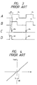
- The phase detector is applied, for example, to a phase-locked loop as shown in Fig. 1. As is well-known in the art, the phase-locked loop comprises, for instance, a
phase detector 1, a low-pass filter 2, a voltage-controlledoscillator 3, and a 1/N frequency divider 4. - The
phase detector 1 receives a signal of a reference frequency fr, compares the phase of the input signal fr and the phase of a signal fv from the 1/N frequency divider 4, and applies the phase detected output KPD to the voltage-controlledoscillator 3 via the low-pass filter 2. The oscillation frequency fout of the voltage-controlledoscillator 3 is controlled so that the two input signals fr and fv to thephase detector 1 may become in-phase with each other, with the result that the output frequency fout becomes equal to N·fr. - Fig. 2 shows the construction of the
conventional phase detector 1. Thephase detector 1 is made up of a phasedifference signal generator 10 and aphase difference detector 14. The phasedifference signal generator 10 includes two D flip-flops NAND gate 13. The two signals fv and fr to be compared in phase are applied to clock input terminals CK of the D flip-flops flops - Phase difference signals φv and φr from output terminals Q of the D flip-
flops NAND gate 13, the output of which is fed to clear terminals CLR of the D flip-flops flops flops - In this way, there can be obtained at the output terminals Q of the D flip-
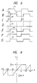
flops phase difference detector 14. Thephase difference detector 14 detects the difference in rise time between the phase difference signals φv and φr and outputs the difference after subjecting it to low-pass filtering. Thus it is possible to obtain a voltage Vout corresponding to the phase difference φ between the two input signals fv and fr. - With the construction of the
phase detector 1 shown in Fig. 2, as the phase difference between the two input signals fv and fr approaches zero, the pulse widths of the phase difference signals φv and φr provided from the output terminals of the D flip-flops - As the result of this, when the phase difference is close to zero, the output voltage of the phase
difference signal generator 10 becomes extremely low and its sensitivity also lowers accordingly. In consequence, the phase difference φ between the two signals fv and fr and the output voltage Vout bear a relationship which is nonlinear in the vicinity of the phase difference φ equal to zero as depicted in Fig. 4, and the gain of thephase detector 1 is reduced accordingly. That is to say, thephase detector 1 has a dead zone ΔD in the vicinity of the phase difference φ equal to zero, and hence is defective in that the output frequency fout of the phase-looked loop varies in the range of the dead zone ΔD. - A phase detector according to the prior art portion of
claim 1 is disclosed in the document US-A-4,378,509. In this prior art the phase difference signal generating means includes first and second flipflops which are supplied at their clock input terminals with the two input signals, and an AND gate which is supplied at one and the other input with the outputs of the first and second flipflops and generates a reset signal for resetting the two flipflops to their initial state, when the outputs are both at a predetermined logic level. A delay circuit is connected between the output of the AND gate and the reset input terminals of the two flipflops causing said phase difference signals to be extended by a time period corresponding to the delay time of the delay circuit. - It is an object of the present invention to provide a phase detector the gain of which does not decrease even when the phase difference between two input signals is close to zero.
- This object is achieved with a phase detector as claimed.
- Specific embodiments of the invention are subject-matter of the dependent claims.
- According to the present invention, the two phase difference signals, which rise at a time interval corresponding to the phase difference between two input signals and fall at the same time, are each appended with a pulse of a width larger than that of the dead zone, and consequently, even if the phase difference between the two input signals is zero, the phase difference detecting means is supplied with the extended phase difference signals of a width larger than that of the dead zone. This enables the phase difference detecting means to stably perform the difference calculating operation, and hence permits avoidance of the reduction of the gain. Thus the present invention prevents the generation of the dead zone in the vicinity of the phase difference equal to zero and offers a phase detector of good linearity.
-
- Fig. 1 is a block diagram showing the construction of a phase-locked loop, showing an example of application of a phase detector;
- Fig. 2 is a connection diagram showing the construction of a conventional phase detector;
- Fig. 3 is a waveform diagram for explaining the operation of the conventional phase detector;
- Fig. 4 is a graph showing the detection characteristic of the conventional phase detector;
- Fig. 5 is a connection diagram illustrating an embodiment of the phase detector according to the present invention;
- Fig. 6 is a waveform diagram for explaining the operation of the phase detector according to the present invention;
- Fig. 7 is a circuit diagram illustrating another embodiment of the present invention;
- Fig. 8 is a graph showing the detection characteristic of the phase detector according to the present invention; and
- Fig. 9 is a circuit diagram illustrating still another embodiment of the present invention.
- In Fig. 5, illustrates an embodiment of the phase detector according to the present invention. The phase detector of the present invention is identical with the prior art example of Fig. 2 in the provision of the phase
difference signal generator 10 for generating two phase difference signals Av and Ar which rise at a time interval corresponding to the phase difference φ between the two input signals fv and fr but fall simultaneously and thephase difference detector 14 which detects the phase difference between the two phase difference signals and outputs a low-frequency component of the difference. According to the present invention, a laggingsignal detecting circuit 15 for detecting the arrival of a lagging one of the two input signals fv and fr, apulse generating circuit 17 responsive to the detected output from the laggingsignal detecting circuit 15 to generate and appendage pulse of a width larger than that ΔD of the dead zone of thephase difference detector 14 and apulse appending circuit 16 for appending the appendage pulse to each of the two phase difference signals output from thephase difference generator 10 are provided between the phasedifference signal generator 10 and thephase difference detector 14. - The lagging
signal detecting circuit 15 is formed by a D flip-flop, for example, and the pulse generating circuit is made up of twoAND gates Q of the D flip-flop 15 and an OR gate 17c for ORing the outputs of the twoAND gates flop 15 has its data input terminal D and clock input terminal CK connected to the output terminals Q of the D flip-flops difference signal generator 10, respectively, and the D flip-flop 15 is supplied with the two phase difference signals Av and Ar. - In the embodiment of Fig. 5 the signal fv is applied to the clock input terminal CK of the one D flip-
flop 11 forming the phasedifference signal generator 10, the data input terminal D of the D flip-flop 15 forming the lagging signal detector is connected to the output terminal Q of the D flip-flop 11, the signal fr is applied to the clock input terminal CK of the D flip-flop 12, and the clock input terminal CK of the D flip-flop 15 forming the lagging signal detector is connected to the output terminal Q of the other D flip-flop 12 forming the phasedifference signal generator 10. - The
AND gate 17A of thepulse generator 17 is supplied at the other input terminal with the input signal fr and theAND gate 17B is supplied at the other input terminal with the input signal fv. If the signal Av provided from the output terminal Q of the D flip-flop 11 has already been at the H level at the point of time when the signal Ar which is provided from the output terminal Q of the D flip-flop 12, that is, if the input signal fr is a lagging signal, than the output at the terminal Q of the D flip-flop 15 goes to the H-logic level at the point of time when the lagging signal fr rises. Consequently, when the input signal fr which is a lagging signal rises and then the phase difference signal Ar rises in response thereto, the D flip-flop 15 reads therein the H-logic output provided at the output terminal Q of the flip-flop 11 and provides an H-logic output at the output terminal Q. Thus, in this instance theAND gate 17A is enabled, through which the input signal fr is output as an appendage pulse Afr to be generated. - On the other hand, in the case where the input signal fr is leading the other input signal fv, when the signal fr rises, the output at the terminal Q of the flip-
flop 12 goes to the high level and at this point the output at the terminal Q of the D flip-flop 11 is low, and the D flip-flop 15 forming the lagging signal detector reads therein the L-logic output from the flip-flop 11. Consequently, in this case, the D flip-flop 15 forming the lagging signal detector outputs the H-logic level at the output terminalQ , and hence theAND gate 17B is enabled, through which the input signal fv is output as an appendage pulse Afv to be generated. - In this way, the
lagging signal detector 15 detects a lagging one of the input signals fv and fr, and theAND gates pulse generator 17 output, as the appendage pulse Afv or Afr, the lagging one of the input signals fv and fr. The appendage pulse Afv or Afr thus produced is provided via theOR gate 17C to thepulse appending circuit 16. Thepulse appending circuit 16 includes twoOR gates flops - Fig. 6 shows the above-described operation. In this example the input signal fv leads the signal fr by φ as shown on Rows A and B. The D flip-
flops lagging signal detector 15 goes high, by which thegate 17A is enabled and the signal fr is output, as the appendage pulse Afr, from thepulse generator 17 as shown on Row E in Fig. 6. In thepulse appending circuit 16 the phase difference signals Av and Ar are respectively appended with the appendage pulse Afr and output as the extended phase difference signals φv and φr shown on Rows F and G in Fig. 6, which are applied to thephase difference detector 14. - In a manner similar to the prior art example of Fig. 2, the
phase difference detector 14 detects the difference between the two extended phase difference signals φv and φr and then outputs a low-frequency component of the difference as a voltage corresponding to the phase difference φ between the input signals fv and fr. Even if the phase difference φ between the two input signals fv and fr is smaller than the width ΔD of the dead zone, thephase difference detector 14 stably operates, because the extended phase difference signals φv and φr each have a pulse width larger than the width ΔD of the dead zone. Assume, however, that the pulse widths of the input signals fv and fr themselves are larger than the dead zone width ΔD. - Fig. 7 illustrates another embodiment of the present invention. The phase
difference signal generator 10, the laggingsignal detector 15, thepulse generator 17 and thepulse appending circuit 16 are exactly identical in construction with those used in the Fig. 5 embodiment, and hence no description will be given of them. In this embodiment thephase difference detector 14 is formed by current-driven circuits so that it is capable of high-speed operations. - A transistor Q1, switching diodes D1, D2 and a transistor Q2 are connected in series, and the types and directions of the transistors Q1 and Q2 and the directions of the diodes D1 and D2 are selected so that constant currents i₁ and i₂ of the same magnitude may flow in the series connection in the same direction (opposite directions with respect to the transistors Q1 and Q2). A +15 V power supply and -15 V power supply are respectively connected via resistors to both ends of the series connection, by which the currents i₁ and i₂ are supplied to the transistors Q1 and Q2 which are effecting constant current operation. The connection point CP of the switching diodes D1 and D2 is connected to an inverting input terminal of an operational amplifier forming a current-voltage converter 14D and is held at a virtual grounding potential. The input transistors Q1 and Q2 have their collectors connected to the anode of a switching diode D3 and the cathode of a switching diode D4, respectively. The extended phase difference signal φv applied to an
input terminal 14B is provided to the cathode of the switching diode D3 via a bias adjusting series-connected diode pair Db1. The extended phase difference signal φr applied to aninput terminal 14C is inverted by aninverter 14E, thereafter being provided to the anode of the switching diode D4 via a bias adjusting series-connected diode pair Db2. - When the extended phase difference signal φv is H-logic, the potential at a connection point P1 is higher than the virtual grounding potential at the connection point CP, so that the switching diode D3 is turned OFF and the switching diode D1 ON. Consequently, the constant current i₁ flowing across the transistor Q1 is applied, as a current +iPD , to the current-voltage converter 14D. When the extended phase difference signal φv is L-logic, the potential at the connection point P1 is a junction voltage of the bias adjusting series-connected diode pair Db1 and hence is lower than the potential at the connection point CP, tuning ON the switching diode D3 and OFF the switching diode D1. Consequently, the constant current i₁ flows into the -15 V power supply via the diode D3 and the current +iPD is zero. On the other hand, when the extended phase difference signal φr is H-logic, the potential at a connection point P2 is a junction voltage of the bias adjusting series-connected diode pair Db2 and hence is l ower than the virtual grounding potential at the connection point CP, so that the switching diode D4 is turned OFF and the switching diode D2 ON. Consequently, the constant current i₂ flowing across the transistor Q2 is supplied as a current -iPD from the current-voltage converter 14D. When the extended phase difference signal φr is L-logic, the potential at the connection point P2 is sufficiently higher than the potential at the connection point CP, turning ON the switching diode D4 and OFF the switching diode D2. Hence the constant current i₂ flowing in the transistor Q2 is supplied from the +15 V power supply via the diode pair Db2 and the diode D4 and the current -iPD is zero.
- As will be seen from the above, when the extended phase difference signals φv and φr are both H-logic, the switching diodes D1 and D2 are simultaneously turned ON and the input currents +iPD and -iPD cancel each other and become zero, with the result that the constant current i₁ in the transistor Q1 flows into the transistor Q2. That is, the output voltage of the current-voltage converter 14D is zero. When the extended phase difference signals φv and φr are both L-logic, the switching diodes D1 and D2 are simultaneously turned OFF, and also in this instance, the output voltage of the current-voltage converter 14D is zero. When the signal φv is H-logic and the signal φr is L-logic, the constant current i₁ flows, as the current +iPD, into the current-voltage converter 14D, from which is provided a voltage corresponding to the current. When the signal φv is L-logic and the signal φr H-logic, the constant current i₂ is supplied, as the current -iPD, to the current-voltage converter 14D, from which is provided a voltage corresponding to the current. The output voltage of the current-voltage converter 14D is averaged by a low-pass filter composed of a capacitor C and a resistor R, thereafter being provided, as the voltage Vout proportional to the phase difference φ between the two input signals fv and fr, to a terminal 14A.
- Fig. 8 shows the phase detection characteristic of the phase detector depicted in Fig. 7. The phase detector according to the present invention is able to perform phase detection with good linearity between π and -π , as shown.
- In the embodiments of Figs. 5 and 7 it is also possible to employ a construction in which the
NAND gate 13 is used also as the laggingsignal detector 15 and thepulse generator 17 is a one-shot multivibrator which outputs pulses of a fixed width. Fig. 9 illustrates such a modification of the Fig. 5 embodiment. One of the input signals fv and fr rises when the output of theNAND gate 13 is H-logic, and then when the other input signal rises, theNAND gate 13 responds thereto to make its output L-logic. In other words, the rise time point of the lagging one of the input signals is thus detected. Triggered by the rise of theNAND gate 13, the one-shot multivibrator 17 outputs an appendage pulse of a width which is, for example, one half the period of the signal fv (equal to the period of the signal fr and longer than the dead zone width ΔD). The appendage pulse thus generated is applied to thepulse appending circuit 16, wherein it is appended to each of the phase difference signals Av and Ar to form the extended phase difference signals φv and φr. - This embodiment is advantageous in that even when the duty ratio of each of the input signal fv and fr is smaller than 50%, the phase difference φ can be detected in the range of from -π to +π . Since the one-shot multivibrator for generating a pulse of a fixed width is difficult to operate at high speed, however, the Fig. 9 embodiment is suitable for phase detection at relatively low frequencies. In contrast to this, the
pulse generator 17 in the embodiments of Figs. 5 and 7 outputs the lagging signal fv or fr detected by the laggingsignal detector 15, as the appendage pulse via thegate phase difference detector 14 becomes narrower than the above-mentioned range of between -π and +π . However, since the laggingsignal detector 15 and thepulse generator 17 are capable of high-speed operation, the embodiments of Figs. 5 and 7 are suitable for phase detection at high frequencies. In particular, in the Fig. 7 embodiment thephase difference detector 14 detects the phase difference while cancelling the in-phase components of the signals φv and φr by switching the currents i₁ and i₂ by the diodes D1 through D4, and hence is capable of operating at far higher speed than thephase difference detector 14 in the Fig. 5 embodiment. - As described above, the present invention employs the construction in which the phase difference signals Av and Ar are each appended with an appendage pulse of a width larger than the width of the dead zone of the
phase difference detector 14 and then are applied thereto--this ensures that the extended phase difference signal Afv or Afr of a pulse width larger than the dead zone width is applied to thephase difference detector 14, even if the phase difference φ between the input signals fv and fr approaches zero. Hence, even if the peak values of the phase difference signals Av and Ar, which are detected in the vicinity of the phase difference φ equal to zero, vary and become small, it is possible to stably perform the phase detection without being affected by such varying peak values of the phase difference signals and eliminate the dead zone of the phase difference detector.
Claims (5)
- A phase detector comprising:
phase difference signal generating means (11, 12) for generating two phase difference signals which rise at a time interval corresponding to the phase difference between two input signals and fall at the same time;
lagging signal detecting means (15) for detecting the arrival of a lagging one of said two input signals;
means (16, 17) to form two extended phase difference signals, and
phase difference detecting means (14) for detecting the difference between said two extended phase difference signals and for outputting a low-frequency component of the detected difference as a voltage corresponding to the phase difference between said two signals,
characterized by
pulse generating means (17) responsive to the detected output of said lagging signal to generate an appendage pulse which rises at the time point of detection of the lagging signal and has a pulse width larger than a predetermined width; and
pulse appending means (16) for appending said appendage pulse to each of said two phase difference signals to form said two extended phase difference signals. - The phase detector of claim 1 wherein said lagging signal detecting means (15) is formed by a D flip-flop which is supplied at its data terminal with the one of said two phase difference signals and at its clock input terminal with the other of said two phase difference signals, and wherein said pulse generating means (17) is formed by first and second AND gates (17A, 17B) which are supplied at one input terminal with a non-inverted output and an inverted output of said D flip-flop, respectively, and at the other input terminals with said two input signals, respectively, and an OR gate (17C) which outputs the OR of the outputs of said first and second AND gates as said additional pulse.
- The phase detector of claim 1 wherein said phase difference signal generating means (11, 12) includes first and second flip-flops which are supplied at their clock input terminals with said two input signals, respectively, and respond to the rising of said input signals to output predetermined logic levels, and AND gate means (13) which is supplied at one and the other input with the outputs of said first and second flip-flops and generates a setting signal for setting said first and second flip-flops to their initial state when their outputs are both said predetermined logic levels, wherein said lagging signal detecting means is used also as said AND gate means, and wherein said pulse generating means (17) is a one-shot multivibrator which responds to said setting signal from said AND gate means to generate said appendage pulse of a fixed width larger than said predetermined width.
- The phase detector of claim 1 wherein said phase difference detecting means includes:
first and second constant-current circuit means (Q₁, Q₂) for supplying constant currents of reverse polarities;
first and second switching diodes (D₁, D₃) having their anodes connected to the output of said first constant-current circuit means (Q₁);
third and fourth switching diodes (D₂, D₄) having their cathodes connected to the output of said second constant-current circuit means (Q₂), the cathode of said first switching diode being connected to the anode of said third switching diode;
current-voltage converting means (14D) connected to the connection point of said first and third switching diodes, for converting an input current thereto into the corresponding voltage;
low-pass filter means (C, R) for averaging the output voltage of said current-voltage converting means and for outputting it as a voltage corresponding to the phase difference between said two input signals;
first bias control means (Db₁) for providing a control bias to the cathode of said second switching diode (D₃) so that when one of said two extended phase difference signals from said pulse appending means has the one logic level, said first and second switching diodes are turned ON and OFF, respectively, and when said one extended phase difference signal has the other logic level, said first and second switching diodes are turned OFF and ON, respectively; and
second bias control means (14E, Db₂) for providing a control bias to the anode of said fourth switching diode (D₄) so that when the other of said two extended phase difference signals from said pulse appending means has the one logic level, said third and fourth switching diodes are turned ON and OFF, respectively, and when said other extended phase difference signal has the other logic level, said third and fourth switching diodes are turned OFF and ON, respectively. - The phase detector of claim 3 or 4 wherein said predetermined width is the width of a dead zone of said phase difference detecting means (14).
Applications Claiming Priority (2)
| Application Number | Priority Date | Filing Date | Title |
|---|---|---|---|
| JP3023449A JPH04262618A (en) | 1991-02-18 | 1991-02-18 | Phase detector |
| JP23449/91 | 1991-02-18 |
Publications (3)
| Publication Number | Publication Date |
|---|---|
| EP0500014A2 EP0500014A2 (en) | 1992-08-26 |
| EP0500014A3 EP0500014A3 (en) | 1992-12-30 |
| EP0500014B1 true EP0500014B1 (en) | 1994-06-15 |
Family
ID=12110815
Family Applications (1)
| Application Number | Title | Priority Date | Filing Date |
|---|---|---|---|
| EP92102607A Expired - Lifetime EP0500014B1 (en) | 1991-02-18 | 1992-02-17 | Phase detector |
Country Status (4)
| Country | Link |
|---|---|
| US (1) | US5266851A (en) |
| EP (1) | EP0500014B1 (en) |
| JP (1) | JPH04262618A (en) |
| DE (1) | DE69200189T2 (en) |
Cited By (5)
| Publication number | Priority date | Publication date | Assignee | Title |
|---|---|---|---|---|
| EP0795955A2 (en) * | 1996-03-15 | 1997-09-17 | Kabushiki Kaisha Toshiba | Phase error signal generator |
| US6329847B1 (en) | 1998-09-29 | 2001-12-11 | U.S. Phillips Corporation | Radio device including a frequency synthesizer and phase discriminator for such a device |
| WO2002009289A2 (en) * | 2000-07-19 | 2002-01-31 | Marconi Communications, Inc. | Phase locked loop having dc bias circuitry |
| WO2003061111A2 (en) * | 2002-01-15 | 2003-07-24 | Microtune (San Diego), Inc. | Phase freqency detector |
| EP1410510A2 (en) * | 2001-03-09 | 2004-04-21 | Ericsson Inc. | Pll cycle slip compensation |
Families Citing this family (28)
| Publication number | Priority date | Publication date | Assignee | Title |
|---|---|---|---|---|
| US5302916A (en) * | 1992-12-21 | 1994-04-12 | At&T Bell Laboratories | Wide range digital frequency detector |
| US5493242A (en) * | 1993-06-30 | 1996-02-20 | Vlsi Technology, Inc. | Status register with asynchronous read and reset and method for providing same |
| US5422918A (en) * | 1993-12-09 | 1995-06-06 | Unisys Corporation | Clock phase detecting system for detecting the phase difference between two clock phases regardless of which of the two clock phases leads the other |
| EP0665650A1 (en) * | 1994-01-31 | 1995-08-02 | STMicroelectronics S.A. | Low voltage high speed phase frequency detector |
| KR960006292A (en) * | 1994-07-28 | 1996-02-23 | 사또 겐이찌로 | Frequency Phase Comparators |
| JPH08139595A (en) * | 1994-11-11 | 1996-05-31 | Mitsubishi Electric Corp | Phase comparator circuit |
| US5684805A (en) * | 1995-11-30 | 1997-11-04 | Brown; Anthony Kevin Dale | Microwave multiphase detector |
| US5703502A (en) * | 1996-05-30 | 1997-12-30 | Sun Microsystems, Inc. | Circuitry that detects a phase difference between a first, base, clock and a second, derivative, clock derived from the base clock |
| US6002282A (en) * | 1996-12-16 | 1999-12-14 | Xilinx, Inc. | Feedback apparatus for adjusting clock delay |
| US5977801A (en) * | 1997-07-07 | 1999-11-02 | International Business Machines Corporation | Self-resetting phase/frequency detector with reduced dead zone |
| US5936430A (en) * | 1997-07-21 | 1999-08-10 | Hewlett-Packard Company | Phase detection apparatus and method |
| US6473439B1 (en) * | 1997-10-10 | 2002-10-29 | Rambus Incorporated | Method and apparatus for fail-safe resynchronization with minimum latency |
| US6429694B1 (en) * | 1998-03-02 | 2002-08-06 | International Business Machines Corporation | Apparatus and method in an integrated circuit for delay line phase difference amplification |
| US6064235A (en) * | 1998-03-18 | 2000-05-16 | International Business Machines Corporation | Shared path phase detector |
| US6407599B1 (en) | 2000-05-10 | 2002-06-18 | Eastman Kodak Company | Method and apparatus for determining a digital phase shift in a signal |
| US6868135B1 (en) | 2000-05-18 | 2005-03-15 | Eastman Kodak Company | Method and apparatus for correcting for a phase shift between a transmitter and a receiver |
| US20020135403A1 (en) * | 2000-06-02 | 2002-09-26 | Enam Syed K. | Trigger circuit |
| JP2005532016A (en) | 2002-06-28 | 2005-10-20 | アドバンスト・マイクロ・ディバイシズ・インコーポレイテッド | Automatic frequency tuning phase lock loop |
| US6729994B1 (en) * | 2002-10-29 | 2004-05-04 | General Motors Corporation | Multi-speed transmission mechanisms with three planetary gearsets and clutch input |
| US7461314B2 (en) * | 2003-06-06 | 2008-12-02 | Advantest Corporation | Test device |
| GB2426879C (en) * | 2003-12-12 | 2008-01-21 | Qualcomm Inc | A phase locked loop that sets gain automatically |
| US7038497B2 (en) * | 2004-04-28 | 2006-05-02 | Seiko Epson Corporation | Differential current mode phase/frequency detector circuit |
| US7411426B2 (en) * | 2004-07-20 | 2008-08-12 | Exar Corporation | Phase detector for RZ |
| US20060017471A1 (en) * | 2004-07-20 | 2006-01-26 | Exar Corporation | Phase detector |
| JP4575816B2 (en) * | 2005-03-23 | 2010-11-04 | 株式会社アドバンテスト | Oscillator for generating a signal based on a reference signal |
| US8585050B2 (en) | 2011-12-06 | 2013-11-19 | Eastman Kodak Company | Combined ultrasonic-based multifeed detection system and sound-based damage detection system |
| US9285206B1 (en) | 2012-02-07 | 2016-03-15 | Pile Dynamics, Inc. | Measurement device for pile displacement and method for use of the same |
| GB2536531A (en) * | 2014-12-19 | 2016-09-21 | Selex Es Ltd | Digital phase meter and phase detection method |
Family Cites Families (9)
| Publication number | Priority date | Publication date | Assignee | Title |
|---|---|---|---|---|
| US4246497A (en) * | 1978-09-29 | 1981-01-20 | Neil Brown Instruments Systems, Inc. | Phase measuring circuit |
| US4264866A (en) * | 1979-01-04 | 1981-04-28 | Ladislav Benes | Frequency and phase comparator |
| US4308500A (en) * | 1979-12-14 | 1981-12-29 | Rca Corporation | Incremental encoder for measuring positions of objects such as rotating shafts |
| US4337435A (en) * | 1980-06-10 | 1982-06-29 | Westinghouse Electric Corp. | Digital phase sequence detector |
| US4378509A (en) * | 1980-07-10 | 1983-03-29 | Motorola, Inc. | Linearized digital phase and frequency detector |
| US4712060A (en) * | 1986-08-29 | 1987-12-08 | Board Of Regents The University Of Texas System | Sampling average phase meter |
| US4901026A (en) * | 1987-07-01 | 1990-02-13 | Rockwell International Corporation | Phase detector circuit having latched output characteristic |
| US4987387A (en) * | 1989-09-08 | 1991-01-22 | Delco Electronics Corporation | Phase locked loop circuit with digital control |
| JPH0736515B2 (en) * | 1989-09-14 | 1995-04-19 | 株式会社東芝 | Phase comparator |
-
1991
- 1991-02-18 JP JP3023449A patent/JPH04262618A/en active Pending
-
1992
- 1992-02-17 EP EP92102607A patent/EP0500014B1/en not_active Expired - Lifetime
- 1992-02-17 DE DE69200189T patent/DE69200189T2/en not_active Expired - Fee Related
- 1992-02-18 US US07/837,206 patent/US5266851A/en not_active Expired - Fee Related
Cited By (6)
| Publication number | Priority date | Publication date | Assignee | Title |
|---|---|---|---|---|
| EP0795955A2 (en) * | 1996-03-15 | 1997-09-17 | Kabushiki Kaisha Toshiba | Phase error signal generator |
| US6329847B1 (en) | 1998-09-29 | 2001-12-11 | U.S. Phillips Corporation | Radio device including a frequency synthesizer and phase discriminator for such a device |
| WO2002009289A2 (en) * | 2000-07-19 | 2002-01-31 | Marconi Communications, Inc. | Phase locked loop having dc bias circuitry |
| EP1410510A2 (en) * | 2001-03-09 | 2004-04-21 | Ericsson Inc. | Pll cycle slip compensation |
| EP1410510A4 (en) * | 2001-03-09 | 2004-07-14 | Ericsson Inc | Pll cycle slip compensation |
| WO2003061111A2 (en) * | 2002-01-15 | 2003-07-24 | Microtune (San Diego), Inc. | Phase freqency detector |
Also Published As
| Publication number | Publication date |
|---|---|
| DE69200189T2 (en) | 1994-11-17 |
| EP0500014A3 (en) | 1992-12-30 |
| DE69200189D1 (en) | 1994-07-21 |
| EP0500014A2 (en) | 1992-08-26 |
| JPH04262618A (en) | 1992-09-18 |
| US5266851A (en) | 1993-11-30 |
Similar Documents
| Publication | Publication Date | Title |
|---|---|---|
| EP0500014B1 (en) | Phase detector | |
| US4623851A (en) | Voltage controlled oscillator using flip-flop controlled switching circuits | |
| US4587496A (en) | Fast acquisition phase-lock loop | |
| US7915963B2 (en) | Current controlled oscillation device and method having wide frequency range | |
| US4156855A (en) | Phase-locked loop with variable gain and bandwidth | |
| EP1780892B1 (en) | Method of operating a radiation hardened phase locked loop | |
| US5495207A (en) | Differential current controlled oscillator with variable load | |
| US20030090327A1 (en) | High-speed and high-precision phase locked loop | |
| US5525932A (en) | Lock indicator for phase locked loop circuit | |
| US5105169A (en) | Current controlled oscillator including conversion of control voltage to regular and thresholded control currents | |
| US3924202A (en) | Electronic oscillator | |
| US5619161A (en) | Diffrential charge pump with integrated common mode control | |
| EP0544109B1 (en) | Phase detector circuit and PLL circuit equipped therewith | |
| KR960001075B1 (en) | Phase detector | |
| JPH06112815A (en) | Charging pump in phase-locked loop | |
| US6940323B2 (en) | Phase locked loop circuit with an unlock detection circuit and a switch | |
| US6140880A (en) | Circuits, architectures and methods for detecting and correcting excess oscillator frequencies | |
| US6188285B1 (en) | Phase-locked loop circuit and voltage-controlled oscillator capable of producing oscillations in a plurality of frequency ranges | |
| US6351154B2 (en) | Phase detector | |
| US6194929B1 (en) | Delay locking using multiple control signals | |
| US5513225A (en) | Resistorless phase locked loop circuit employing direct current injection | |
| US6496077B2 (en) | Phase detector for automatically controlling offset current and phase locked loop including the same | |
| US4270093A (en) | Apparatus for forcing a phase-lock oscillator to a predetermined frequency when unlocked | |
| JPH04282905A (en) | Phase detector | |
| US5694086A (en) | Precision, analog CMOS one-shot and phase locked loop including the same |
Legal Events
| Date | Code | Title | Description |
|---|---|---|---|
| PUAI | Public reference made under article 153(3) epc to a published international application that has entered the european phase |
Free format text: ORIGINAL CODE: 0009012 |
|
| 17P | Request for examination filed |
Effective date: 19920217 |
|
| AK | Designated contracting states |
Kind code of ref document: A2 Designated state(s): DE FR GB |
|
| PUAL | Search report despatched |
Free format text: ORIGINAL CODE: 0009013 |
|
| AK | Designated contracting states |
Kind code of ref document: A3 Designated state(s): DE FR GB |
|
| 17Q | First examination report despatched |
Effective date: 19930513 |
|
| GRAA | (expected) grant |
Free format text: ORIGINAL CODE: 0009210 |
|
| AK | Designated contracting states |
Kind code of ref document: B1 Designated state(s): DE FR GB |
|
| RIN1 | Information on inventor provided before grant (corrected) |
Inventor name: NUKUI, YOSHIHIRO |
|
| REF | Corresponds to: |
Ref document number: 69200189 Country of ref document: DE Date of ref document: 19940721 |
|
| ET | Fr: translation filed | ||
| PLBE | No opposition filed within time limit |
Free format text: ORIGINAL CODE: 0009261 |
|
| STAA | Information on the status of an ep patent application or granted ep patent |
Free format text: STATUS: NO OPPOSITION FILED WITHIN TIME LIMIT |
|
| 26N | No opposition filed | ||
| PG25 | Lapsed in a contracting state [announced via postgrant information from national office to epo] |
Ref country code: FR Effective date: 19951031 |
|
| REG | Reference to a national code |
Ref country code: FR Ref legal event code: ST |
|
| PG25 | Lapsed in a contracting state [announced via postgrant information from national office to epo] |
Ref country code: GB Effective date: 19960217 |
|
| GBPC | Gb: european patent ceased through non-payment of renewal fee |
Effective date: 19960217 |
|
| PGFP | Annual fee paid to national office [announced via postgrant information from national office to epo] |
Ref country code: DE Payment date: 19990225 Year of fee payment: 8 |
|
| PG25 | Lapsed in a contracting state [announced via postgrant information from national office to epo] |
Ref country code: DE Free format text: LAPSE BECAUSE OF NON-PAYMENT OF DUE FEES Effective date: 20001201 |