EP0500293A2 - Particle detection method and apparatus - Google Patents
Particle detection method and apparatus Download PDFInfo
- Publication number
- EP0500293A2 EP0500293A2 EP92301275A EP92301275A EP0500293A2 EP 0500293 A2 EP0500293 A2 EP 0500293A2 EP 92301275 A EP92301275 A EP 92301275A EP 92301275 A EP92301275 A EP 92301275A EP 0500293 A2 EP0500293 A2 EP 0500293A2
- Authority
- EP
- European Patent Office
- Prior art keywords
- degrees
- angle
- light
- meridional
- mirror
- Prior art date
- Legal status (The legal status is an assumption and is not a legal conclusion. Google has not performed a legal analysis and makes no representation as to the accuracy of the status listed.)
- Granted
Links
- 239000002245 particle Substances 0.000 title claims abstract description 34
- 238000001514 detection method Methods 0.000 title description 5
- 238000000034 method Methods 0.000 claims abstract description 37
- 238000009304 pastoral farming Methods 0.000 claims abstract description 17
- 230000000873 masking effect Effects 0.000 claims description 7
- 239000004065 semiconductor Substances 0.000 abstract description 18
- 239000000919 ceramic Substances 0.000 abstract description 7
- 235000012431 wafers Nutrition 0.000 description 37
- 244000046052 Phaseolus vulgaris Species 0.000 description 8
- 235000010627 Phaseolus vulgaris Nutrition 0.000 description 8
- 230000007547 defect Effects 0.000 description 8
- 230000003287 optical effect Effects 0.000 description 7
- 239000000356 contaminant Substances 0.000 description 6
- 238000007689 inspection Methods 0.000 description 6
- 239000000758 substrate Substances 0.000 description 6
- 238000005286 illumination Methods 0.000 description 5
- 239000013307 optical fiber Substances 0.000 description 4
- 230000008901 benefit Effects 0.000 description 3
- 239000000835 fiber Substances 0.000 description 3
- 239000000463 material Substances 0.000 description 3
- XKRFYHLGVUSROY-UHFFFAOYSA-N Argon Chemical compound [Ar] XKRFYHLGVUSROY-UHFFFAOYSA-N 0.000 description 2
- 238000000149 argon plasma sintering Methods 0.000 description 2
- 239000002184 metal Substances 0.000 description 2
- 238000012986 modification Methods 0.000 description 2
- 230000004048 modification Effects 0.000 description 2
- 230000004044 response Effects 0.000 description 2
- 230000032683 aging Effects 0.000 description 1
- 238000004458 analytical method Methods 0.000 description 1
- 229910052786 argon Inorganic materials 0.000 description 1
- 238000010276 construction Methods 0.000 description 1
- 238000011109 contamination Methods 0.000 description 1
- 230000001419 dependent effect Effects 0.000 description 1
- 239000011521 glass Substances 0.000 description 1
- 238000003384 imaging method Methods 0.000 description 1
- 239000012535 impurity Substances 0.000 description 1
- 230000007774 longterm Effects 0.000 description 1
- 238000004519 manufacturing process Methods 0.000 description 1
- 230000007246 mechanism Effects 0.000 description 1
- 238000001465 metallisation Methods 0.000 description 1
- 230000007935 neutral effect Effects 0.000 description 1
- 230000008569 process Effects 0.000 description 1
- 238000011084 recovery Methods 0.000 description 1
- 229910052724 xenon Inorganic materials 0.000 description 1
- FHNFHKCVQCLJFQ-UHFFFAOYSA-N xenon atom Chemical compound [Xe] FHNFHKCVQCLJFQ-UHFFFAOYSA-N 0.000 description 1
Images


Classifications
-
- G—PHYSICS
- G01—MEASURING; TESTING
- G01N—INVESTIGATING OR ANALYSING MATERIALS BY DETERMINING THEIR CHEMICAL OR PHYSICAL PROPERTIES
- G01N21/00—Investigating or analysing materials by the use of optical means, i.e. using sub-millimetre waves, infrared, visible or ultraviolet light
- G01N21/84—Systems specially adapted for particular applications
- G01N21/88—Investigating the presence of flaws or contamination
- G01N21/95—Investigating the presence of flaws or contamination characterised by the material or shape of the object to be examined
- G01N21/9501—Semiconductor wafers
-
- G—PHYSICS
- G01—MEASURING; TESTING
- G01N—INVESTIGATING OR ANALYSING MATERIALS BY DETERMINING THEIR CHEMICAL OR PHYSICAL PROPERTIES
- G01N21/00—Investigating or analysing materials by the use of optical means, i.e. using sub-millimetre waves, infrared, visible or ultraviolet light
- G01N21/84—Systems specially adapted for particular applications
- G01N21/88—Investigating the presence of flaws or contamination
- G01N21/94—Investigating contamination, e.g. dust
-
- G—PHYSICS
- G01—MEASURING; TESTING
- G01N—INVESTIGATING OR ANALYSING MATERIALS BY DETERMINING THEIR CHEMICAL OR PHYSICAL PROPERTIES
- G01N21/00—Investigating or analysing materials by the use of optical means, i.e. using sub-millimetre waves, infrared, visible or ultraviolet light
- G01N21/17—Systems in which incident light is modified in accordance with the properties of the material investigated
- G01N21/47—Scattering, i.e. diffuse reflection
- G01N2021/4704—Angular selective
- G01N2021/4707—Forward scatter; Low angle scatter
-
- G—PHYSICS
- G01—MEASURING; TESTING
- G01N—INVESTIGATING OR ANALYSING MATERIALS BY DETERMINING THEIR CHEMICAL OR PHYSICAL PROPERTIES
- G01N21/00—Investigating or analysing materials by the use of optical means, i.e. using sub-millimetre waves, infrared, visible or ultraviolet light
- G01N21/17—Systems in which incident light is modified in accordance with the properties of the material investigated
- G01N21/47—Scattering, i.e. diffuse reflection
- G01N21/4738—Diffuse reflection, e.g. also for testing fluids, fibrous materials
- G01N21/474—Details of optical heads therefor, e.g. using optical fibres
- G01N2021/4742—Details of optical heads therefor, e.g. using optical fibres comprising optical fibres
Definitions
- the present invention relates generally to a method and apparatus for detecting the presence of particles on the surface of an object and more particularly to a method and apparatus for detecting and measuring the number and sizes of contaminant particles on the surface of an object, such as a patterned or virgin semiconductor wafer or ceramic tile, using the principle of light scattering.
- the system which corresponds generally to the above-described Surfscan TM 7000, includes a light source for emitting a beam of light.
- a polarizing filter is used to polarize the bean of light in a direction substantially parallel to the surface of the patterned semiconductor wafer to be examined.
- the beam is enlarged in. cross-sectional diameter by a beam expander placed along the path of the beam after the polarizing filter. The beam is then caused to scan by a deflection mirror.
- a telecentric lens brings the scanning beam to focus on the patterned wafer at a shallow angle of incidence, the beam striking the wafer surface substantially parallel to the pattern streets formed on the wafer.
- a light collection system for detecting side scattered light is positioned in the plane of the scan line.
- the light collection system which includes a tens for focusing the side scattered light, a polarizing fitter oriented in a direction substantially parallel to the surface of the patterned wafer, and a photomultiplier tube for detecting light incident thereon and transmitting electrical signals in response thereto, receives light scattered in a direction less than 15 degrees above the surface and at angle relative to the beam direction in a range from about 80 degrees to 100 degrees.
- a processor constructs templates from the electrical signal corresponding to individual patterns and compares the templates to identify particles,
- the system comprises a light source combined with a collimator.
- a beam splitter splits the incident beam into a first beam, which is directed to the wafer, and a second beam, which is directed to a light absorbing surface.
- the wafer is mounted on a tilted rotatable support.
- An aperture plate limits the size of the light beam incident upon the sample and at the same time restricts the amount of light reflected back along the direction of the incident beam to a photomultiplier by the surface defects.
- the incident beam is split by the wafer, the planar surface of the wafer directing the major portion of the beam back to the back side of the aperture plate whereas the defects on the wafer direct a portion of the beam back through the aperture plate.
- the portion of the beam transmitted through the aperture plate strikes a beam splitter and is directed through a telescope to a photomultiplier.
- an inspection apparatus for detecting unfavorable foreign natters existent. on the surface of an object such as a semiconductor wafer.
- the apparatus includes a collimated beam generator portion which projects a collimated beam towards the object to be inspected from a side thereof and a mechanism which senses light reflected from the surface of the object, through a polarizer plate.
- the signal-to-noise ratio between a detection signal generated by a pattern of the foreign matter to be detected and a signal generated by a normal pattern of the object surface and sensed as a noise component are said to be enhanced.
- a surface irregularity analyzing system which includes structure for directing light towards a surface in a direction having a certain angular relationship to the surface. If the light strikes irregularities in the surface it is reflected in a direction having an angular relationship to the surface other than equal and opposite the incident direction. The amount of light reflected from irregularities in the surface is determined, either photographically or photoelectrically using a detector positioned over the surface, to provide an analysis of irregularities in the surface.
- the present invention is concerned with providing a new and improved method and apparatus for detecting the presence of contaminant particles on a surface of an object using the principle of scattered light.
- an apparatus for detecting particles on the surface of an object comprises (a) means for providing a beam of light; (b) means for bringing said beam to focus on the surface at a grazing angle of incidence; and (c) means for detecting forward scattered light from the surface.
- forward scattered light is to be contrasted with the terms “back scattered light” and “side scattered light” and is not intended to encompass, as is the case with U.S. Pat. No. 4,898,471, forwardly- directed scattered light of the type that would ordinarily be collected by typical focusing optics positioned along the plane of a scan line to receive side scattered light.
- the present invention is directed to a method and apparatus for detecting contaminant particles present on the surface of an object.
- the invention is based, in part, on the discovery that improved signal to background and signal to noise ratios may be obtained by bringing a beam of light to focus on the surface of the object at a grazing angle and measuring forward scattered light from the surface.
- the forward scattered light is observed at a meridional angle of about 5 to 60 degrees, more preferably at about 30 degrees, and at an azimuthal angle of about 2 to about 10 degrees, more preferably at about 4 degrees.
- meridional angle is the angle between the plane of incidence of the illumination bean and the observation bean
- azimuthal angle is the angle between the observation beam and the surface being inspected.
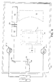
- FIG. 1 there is illustrated an apparatus for detecting particles on a surface of an object, the apparatus being constructed according to the teachings of the present invention and represented generally by reference numeral 11.
- Apparatus 11 includes a laser 13 for outputting a beam of laser light 15.
- laser 13 is a 40 mW Nd:YAG laser which produces monochromatic light at 532 nm.
- Beam 15 is first expanded in cross-section and caused to converge by an expander 17 and is then deflected by a galvanometer 19 which causes the beam to scan in the y-direction, preferably at a rate of about 50/sec.
- the beam then passes through an Fe lens 21 which brings the beam to focus as a small spot or point on a straight scan line 23 on a specimen S, such as a semiconductor wafer or a tile, at a grazing angle a.
- Grazing angle a is preferably an angle of between about 80 degrees and 90 degrees from the normal to the specimen surface (i.e., between 0 and about 10 degrees from the plane of the specimen surface), more preferably an angle of about 80 degrees from the normal to the specimen surface.
- the specimen is mounted on a holder (i.e. stage) 24 which is in the form of a vacuum chuck.
- Holder 24 is mounted such that it can be moved in the x-direction so that the entire surface of the specimen can be illuminated, a scan line at a time.
- holder 24 moves at such a speed that the entire surface of the specimen can be illuminated in about 20 seconds.
- the light scattered from the specimen is detected by pair of photomultiplier tubes 25-1 and 25-2, which are preferably disposed at a meridional angle of about 30 degrees and at an azimuthal angle of about 4 degrees.
- the electrical signals outputted by photomultiplier tubes 25 are then fed into a computer 27 for processing and displayed on a display 29.
- the entire apparatus 11, except for computer 27 and display 29, is enclosed within a light tight housing 31 so that extraneous light is not mistakenly detected.
- a light tight housing 31 Preferably, the inner walls of housing 31 are coated with a dark, non-reflective surface.
- the meridional angle between the incident beam and the observation beam is not constant over the entire length of the scan line. This is best visualized by referring to Fig. 1 and noting the difference in angles b and c. As discussed above, because certain meridional angles, such as the 30 degree angle, have been found to optimize the signal to background and signal to noise ratios, it is clearthat keeping the meridional angle constant over the length of the scan line is highly desirable.
- FIG. 2-8 there is illustrated another embodiment of an apparatus for detecting particles on a surface of an object, such as a virgin or patterned semiconductor wafer, ceramic tile, or the like, the apparatus being constructed according to the teachings of the present invention and represented generally by reference numeral 41.
- apparatus 41 solves the problem encountered by apparatus 11 of keeping the meridional angle of observation constant over the entire length of the scan line.
- Apparatus 41 includes a housing 43 (not shown in Fig. 2) which is light tight and whose inner waits are coated with a dark, non-reflective material.
- housing 43 Preferably, the dimensions of housing 43 are 24 inches in length, 18 inches in width, and 20.5 inches in depth.
- An optical plate 44 (not shown in Fig. 2), which is also coated with a dark, non-reflective surface, is mounted within housing 41 to support some of the optical components to be discussed below.
- a laser 45 which produces an intense beam of collimated light, is disposed within housing 43 on plate 44.
- laser 45 is a 40 mW Nd: YAG laser with an output at 532 nm.
- the beam generated by laser 45 is passed through a variable neutral density filter 46, which may attenuate the beam, and an expander 47, whose first lens 49 enlarges the cross-sectional diameter of the beam by a magnitude of about 10 and whose second lens 51 causes the bean to converge.
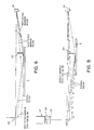
- the beam After emerging from expander 47, the beam is deflected off a 45 degree mirror 53, which directs the beam to a scanning mirror 55 of a galvanometer 57.
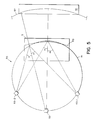
- galvanometer 57 is set so that mirror 55 scans approximately 50 times per second. Scanning mirror 55 deflects the beam downwardly through a hole in optical plate 44 where it is deflected off a 45 degree mirror 59 disposed at the center of a circle defined by an off-axis hypertelecentric mirror 61.
- mirror 59 is merely to alter the direction of the scanning beam so as to permit apparatus 41 to be reduced in size and that mirror 59 could be eliminated, as seen in Fig. 5(a), by placing mirror 55 of galvanometer 57 where mirror 59 is shown in Fig. 5.
- Hypertelecentric mirror 61 which is angled downwardly about 5 degrees, brings the beam deflected by mirror 59 to focus as a curved scan line 89 on a specimen S at a grazing angle of preferably between about 80 and 90 degrees from the normal to the specimen, more preferably at about 80 degrees from the normal to the specimen.
- mirror 59 is disposed at the center of a 1110 mm diameter circle 87 (partially shown in Fig. 5) defined by mirror 61, the light beam comes to focus on the specimen S as an arcuate scan line 89 having a length of about 200 mm and whose nidpoint is about 375 nm from mirror 59.
- specimen S is a patterned object
- optimum results are obtained if the light bean strikes the specimen surface at an angle which is not parallel to the direction of the streets of the pattern, but rather, as set forth in U.S. Pat. No. 4,772,126, which issued September 20, 1988 with inventors C.D. Allemand et al., at about a 45 degree angle relative to the pattern streets.
- the light scattered from the specimen S is deflected by a pair of symmetrically disposed mirrors 63-1 and 63-2, which direct the scattered light to respective sets of lenses 65-1 and 65-2 and detectors 67-1 and 67-2.
- mirrors 63-1 and 63-2 are used merely to reduce the size of the apparatus and that they could be eliminated, as seen in Fig. 5(a), by positioning lenses 65 and/or detectors 67 where mirrors 63 are currently shown in Fig.
- mirrors 63-1 and 63-2, mirror 59, and arcuate scan line 89 are positioned so that when viewed from directly above they appear to lie along the circumference of an imaginary circle 91.
- Mirrors 63 are disposed at a meridional angle of preferably 5-60 degrees, more preferably 30 degrees, and at an azimuthal angle of preferably 2-10 degrees, more preferably 4 degrees.
- the light deflected by mirrors 63-1 and 63-2 passes through respective holes in optical plate 44 and is focused by lenses 65-1 and 65-2, which are preferably 30 mn bi-convex lenses, onto a pair of detectors 67-1 and 67-2.
- lenses 65-1 and 65-2 which are preferably 30 mn bi-convex lenses, onto a pair of detectors 67-1 and 67-2.
- One advantage to using a pair of symmetrically disposed detectors, instead of a single detector, to measure the scattered light is that one can maintain an optimum signal to noise ratio as the illumination bean moves across the scan line.
- the intensity of the detected light signal varies as a function of the distance between the detector and that point of the scan line being illuminated.
- the variation in the intensity of the light signal as a function of distance can be corrected using computer software; however, because the amount of noise calculated by the computed will itself he dependent upon the signal detected, an optimum signal to noise ratio will not be attained.
- the intensity of the signal will be more constant over the entire scan line, permitting a better signal to noise ratio to be achieved.
- Each detector 67 includes an optical fiber 69, onto which the light focused by lens 65 is imaged, and a photomultiplier tube 71, which is optically coupled to the output of fiber 69.
- the output of fiber 69 and the input of tube 71 are brought into contact with a contact gel (not shown).
- the reason for using optical fiber 69 rather than imaging the scan line directly onto tube 71 is that the photocathode of tube 71 does not have a uniform response across its surface. Consequently, when the scan line is imaged onto the photocathode, the signal shows up stronger at the center of the photocathode and weaker radially outward. To correct for this lack of uniformity, the scan line is imaged by lens 65 onto fiber 69 which converges it to a small circle (e.g., 8-10 mm) on photomultiplier tube 71.
- a small circle e.g. 8-10 mm
- the outputs from tubes 71 are processed by a computer 73, which adds the signals using a fixed circuit or which adjusts each signal to account for the possibly different distances from the point of scattering to the respective detectors and then adds the signals.
- a computer 73 which adds the signals using a fixed circuit or which adjusts each signal to account for the possibly different distances from the point of scattering to the respective detectors and then adds the signals.
- an "and" gate could be used for the following reason: Because two photomultiplier tubes are used, the maximum background signal may not appear at the same tine for each photomultiplier tube whereas the maximum particle signal appears simultaneously on both tubes.
- the specimen is mounted on a holder 77, which is preferably a vacuum chuck.
- Holder 77 is mounted on a stage 79, which is preferably a telescoping stage to facilitate the mounting and removal of the substrate from holder 77.
- Holder 77 is mechanically coupled through a shaft to a motor 81 which causes holder 77 to slide on top of stage 79 in the direction of mirror 61. In this way, over a period of about 20 seconds, the entire surface of the specimen can be illuminated, one scan line at a time.
- motor 81 may be coupled to computer 73 so that the speed at which holder 77 slides towards mirror 61 may be adjusted.
- FIG. 5 a plan view of that portion of apparatus 41 that is represented by reference numeral 85 in Fig. 3 is shown in order to illustrate how the geometric configuration of apparatus 41 solves the problem discussed above in connection with apparatus 11, namely, the problem of keeping the meridional angle of observation constant along the entire scan line.
- FIG. 5 when mirror 59, mirrors 63-1 and 63-2, and scan line 89 are viewed from directly above, they appear to be situated on the circumference of an imaginary circle 91. (It is to be understood that one or more of mirror 59, mirrors 63, and scan line 89 may be located on different planes and that while mirror 59 and mirrors 63-1 and 63-2 are shown in Fig.
- mirrors 59 and 63 could be replaced with galvanometer 57 and/or lenses 65-1 and 65-2, respectively.) Because mirror 59, mirrors 63, and scan line 89 are thus situated, the meridional angle of observation m for each detector will be the same at every point along the length of the scan line. Moreover, because mirrors 63 are symmetrically disposed, preferably at about a 30 degree angle relative to mirror 59, the meridional angle of observation m will be the same for both detectors.
- the diameter of circle 87 is 1110 mm and the midpoint of scan line 89 is about 375 mm from mirror 61, the diameter of circle 91 will be approximately 382 mm.
- the trapping and masking components of apparatus 41 are used to trap the light that is reflected off, rather than scattered by, the specimen. If the reflected light is not trapped, it might otherwise find its way to the detectors and be picked up as background.
- the trapping components include a trapping mirror 97 and a trap 99.
- Trapping mirror 97 which deflects the reflected beam into trap 99, is preferably placed along the path of the reflected beam at the point where it converges to a point, i.e., at approximately the center of the circle defined by mirror 61.
- Trap 99 may be a conventional light trap consisting of a multi-walled enclosure which is coated with a dark, non-reflective material.
- the masking components for apparatus 41 are used to minimize the amount of light picked up by the detectors as a result of scattering of the beam by mirror 61.
- the masking components include a scan line mask 101, a pair of mirror scatter masks 103-1 and 103-2, and four focal masks 105-1 through 105-4.
- Scan line mask 101 is a curved, dark, non-reflective wall disposed a short distance over the scan line.
- Mask 101 masks the light scattered by mirror 61 which, if left unmasked, would strike the substrate and possibly be reflected off mirror 63 (see Fig. 6).
- Mirror scatter masks 103-1 and 103-2 which are flat, dark, non-reflective walls, extend backwards and inwards from either side of mask 101.
- Masks 103-1 and 103-2 mask the lightwhich is scattered by mirror 61 directly onto mirror 63 (see Fig. 7). Masks 103-1 and 103-2, however, do not extend so far downwardly that the signal beam becomes masked.
- Focal masks 105 a pair of which are disposed between each lens 65 and detector 67 on the image plane of lens 65, also mask the light which is scattered by mirror 61 directly onto mirror 63 (see Fig. 8).
- apparatus 41 may be used to detect particles on the surfaces of both virgin and patterned semiconductor wafers, ceramic tiles, and the like, it has been found that illumination of the pattern on patterned objects causes diffraction of the light beam, which may then be detected by detectors 67-1 and 67-2, thereby creating the possibility that an erroneous indication of the presence of a particle may occur.
- FIG. 9 there is shown an embodiment of an apparatus constructed according to the teachings of the present invention for detecting particles on the surface of a patterned object, such as a semiconductor wafer, ceramic tile, or the like, the apparatus being represented generally by reference numeral 151.
- Apparatus 151 is similar in construction and operation to apparatus 41, the only difference between the two being that apparatus 151 additionally includes a pair of identical masks 153-1 and 153-2, mask 153-1 being disposed between mirror 63-1 and lens 65-1 and mask 153-2 being disposed between mirror 63-2 and lens 65-2.
- each mask 153 preferably comprises a transparent substrate 155, such as a glass slide or the like, onto which are marked one or more non-transparent bands 157, which correspond to the diffraction pattern created by illumination of the patterned specimen S being examined.
- the specific arrangement of bands 157 on substrate 155 will depend upon the particular configuration of the pattern imprinted on the specimen.
- detectors 67-1 and 67-2 are replaced with a pair of optical fibers (or with a bifurcated optical fiber) which are optically coupled, preferably through a contact gel, to a single photomultiplier tube.
Abstract
Description
- The present invention relates generally to a method and apparatus for detecting the presence of particles on the surface of an object and more particularly to a method and apparatus for detecting and measuring the number and sizes of contaminant particles on the surface of an object, such as a patterned or virgin semiconductor wafer or ceramic tile, using the principle of light scattering.
- There are a variety of existing ways for detecting and measuring the number and sizes of particles on the surface of a semiconductor wafer for the purpose of rejecting those wafers which have on their surface one or more particles above certain sizes or an excessive number of particles. One of the more simple methods involves having a human operator inspect the wafer using a light field/dark field microscope. Using the eye, the operator actually counts the number of articles and also identifies the size of the particles, such as those between 1 to 20 microns, and then rejects those wafers which have particles of or above a certain size or which have an excessive number of particles. This method, however, is highly inaccurate and very expensive both in terms of wages for the human operator and in terms of the number of rejects both after the inspection and after production of the chips (when an erroneously passed wafer is found to have an electrical defect, e.g., short circuits, because of the presence of contaminant particles).
- In P. Burggraaf, "Auto Wafer Inspection: Tools for Your Process Problems," Semiconductor International, pp. 54-61 (December 1988), there are disclosed several types of automatic-vision wafer inspection systems, i.e., systems which do not require a human inspector. One type of system described is the Surfscan TM 7000 manufactured by Tencor Instruments, Mountain View, California. This light scattering system. uses a laser bean, focused by a telecentric lens, to scan a patterned semiconductor wafer at a shallow angle of incidence, the patterned semiconductor wafer being aligned so that the pattern streets run parallel to the direction of scanning. Side scattered light from the wafer is then detected by a single photomultiplier tube disposed to the side of the wafer in the plane of the scan line.
- In U.S. Pat. No. 4,898,471, issued February 6, 1990, and assigned to Tencor Instruments, a system for detecting particles and other defects on a patterned semiconductor wafer, photomask, or the like is disclosed. The system, which corresponds generally to the above-described Surfscan TM 7000, includes a light source for emitting a beam of light. A polarizing filter is used to polarize the bean of light in a direction substantially parallel to the surface of the patterned semiconductor wafer to be examined. The beam is enlarged in. cross-sectional diameter by a beam expander placed along the path of the beam after the polarizing filter. The beam is then caused to scan by a deflection mirror. A telecentric lens brings the scanning beam to focus on the patterned wafer at a shallow angle of incidence, the beam striking the wafer surface substantially parallel to the pattern streets formed on the wafer. A light collection system for detecting side scattered light is positioned in the plane of the scan line. The light collection system, which includes a tens for focusing the side scattered light, a polarizing fitter oriented in a direction substantially parallel to the surface of the patterned wafer, and a photomultiplier tube for detecting light incident thereon and transmitting electrical signals in response thereto, receives light scattered in a direction less than 15 degrees above the surface and at angle relative to the beam direction in a range from about 80 degrees to 100 degrees. A processor constructs templates from the electrical signal corresponding to individual patterns and compares the templates to identify particles,
- In U.S. pat. No. 4,772,126 to C.D. Allemand etal., there is disclosed a method and apparatus for detecting the presence of particles on the surface of an object such as the front side of a patterned semiconductor wafer. A vertically expanded, horizontally scanning, beam of light is directed onto an area on the surface of the object at a grazing angle of incidence. A video camera positioned above the surface detects light scattered from any particles which may be present on the surface, but not specularly reflected light. The surface is angularly prepositioned (rotated) relative to the incident light beam so that the diffracted light from the surface and the pattern of lines on the surface is at a minimum. The object is then moved translationally to expose another area to the incident light beam so that the entire surface of the object or selected portions thereof can be examined, one area at a time.
- In U.S. Pat. No. 4,377,340 to G.P. Green et al., there is disclosed a method and apparatus for detecting and measuring the number and sizes of impurities on the surface of a material, such as a semiconductor wafer, wherein a beam of high intensity collimated light from a xenon arc lamp is directed onto the surface at normal incidence in the absence of any extraneous light, through a collimating mirror and a pin hole device and whereat the particles will scatter the light, and wherein the surface is viewed by a high light sensitive TV camera which is positioned off-axis to pick up scattered light but not specularly reflected light for display on a viewing screen.
- In IBM Technical Disclosure Bulletin, Volume 12, No. 10, pp. 1672-1673, dated March, 1970, there is disclosed a system for detecting repeated geometric defects on a reflecting surface. The system comprises a light source combined with a collimator. A beam splitter splits the incident beam into a first beam, which is directed to the wafer, and a second beam, which is directed to a light absorbing surface. The wafer is mounted on a tilted rotatable support. An aperture plate limits the size of the light beam incident upon the sample and at the same time restricts the amount of light reflected back along the direction of the incident beam to a photomultiplier by the surface defects. The incident beam is split by the wafer, the planar surface of the wafer directing the major portion of the beam back to the back side of the aperture plate whereas the defects on the wafer direct a portion of the beam back through the aperture plate. The portion of the beam transmitted through the aperture plate strikes a beam splitter and is directed through a telescope to a photomultiplier.
- In IBM Technical Disclosure Bulletin,
Volume 21, No. 6, pp. 2336-2337, dated November, 1978, there is disclosed a system for detecting defects on wafers wherein light from a plurality of ring light sources impinges on the wafer at an oblique angle to the wafer surface and wherein light scattered upward from the surface at right angles thereto is fed by a lens system into a broad band array detector. - In IBM Technical Disclosure Bulletin,
Volume 27, No. 12, pp. 6971-6973, dated May, 1985, there is disclosed an inspection system for particulate and defect detection on product wafers wherein light from an illuminatDr impinges on the substrate at an angle of 0 to 5 degrees. Additionally, the beam is oriented at a preferred angle, e.g., 45 degrees, with respect to the wafer circuit geometry. A photomultiplier tube is arranged above the substrate to monitor light scattered therefrom. - In IBM Technical Disclosure Bulletin
Volume 27, No. 12, pp. 6999-7001, dated May, 1985, there is disclosed an automated, grazing angle, oblique light, inspection system for the detection of particulate contamination and metallization defects on semiconductor product wafers. - In U.S. Pat. No. 2,947,212 to R.C. Woods, there is disclosed a method of detecting surface conditions on a strip of sheet metal having line markings in which light from a light source is directed towards the surface of the sheet metal in a direction generally perpendicular to the line markings. Non-specular reflection in a selected direction which is perpendicular to the lines, and which is preferably between the angle of incidence and the angle of specular reflection, is monitored by a photoelectric cell which is able to detect a surface flaw by variation in the intensity of the reflected light. The light in the incident beam may be polarized and the light in the selected non-specular reflected bean filtered to pass only such polarized light.
- In U.S. Pat. No. 4,342,515 to M. Akiba et a!., there is disclosed an inspection apparatus for detecting unfavorable foreign natters existent. on the surface of an object such as a semiconductor wafer. The apparatus includes a collimated beam generator portion which projects a collimated beam towards the object to be inspected from a side thereof and a mechanism which senses light reflected from the surface of the object, through a polarizer plate. In accordance with the disclosed technique for using the apparatus, the signal-to-noise ratio between a detection signal generated by a pattern of the foreign matter to be detected and a signal generated by a normal pattern of the object surface and sensed as a noise component are said to be enhanced.
- In U.S. Pat. No. 3,782,836 to C.F. Fey et al., there is disclosed a surface irregularity analyzing system which includes structure for directing light towards a surface in a direction having a certain angular relationship to the surface. If the light strikes irregularities in the surface it is reflected in a direction having an angular relationship to the surface other than equal and opposite the incident direction. The amount of light reflected from irregularities in the surface is determined, either photographically or photoelectrically using a detector positioned over the surface, to provide an analysis of irregularities in the surface.
- In Japanese Patent no. 61-162738 assigned to Hitachi, Ltd., there is disclosed a method for preventing a circuit pattern from being misjudged to a foreign matter, the method employing a flat spot-shaped scan laser beam.
- The present invention is concerned with providing a new and improved method and apparatus for detecting the presence of contaminant particles on a surface of an object using the principle of scattered light.
- It is considered advantageous in the present invention to provide a method and apparatus as described above which can be used to detect the presence of contaminant particles on both virgin and patterned semiconductor wafers, ceramic tiles and the like.
- It is further considered advantageous in the present invention to provide a method and apparatus as described above in which the signal to background ratio and the signal to noise ratio are optimized.
- It is still further considered advantageous in the present invention to provide a method and apparatus as described above which is capable of detecting contaminant particles as small as about 0.8 microns on patterned tiles.
- It is also considered advantageous in the present invention to provide a method and apparatus as described above which is designed especially for use in dark field illumination applications.
- The aforementioned features and advantages of the present invention, will be set forth in part in the description which follows, and in part will be obvious from the description or may be learned by practice of the invention. The objects, features, and advantages of the invention may be realised and attained by means of the instrumentalities and (a) providing a beam of light; (b) bringing said beam to focus on the surface at a grazing angle of incidence; and (c) detecting forward scattered light from the surface.
- Also in accordance with the teachings of the present invention, an apparatus for detecting particles on the surface of an object comprises (a) means for providing a beam of light; (b) means for bringing said beam to focus on the surface at a grazing angle of incidence; and (c) means for detecting forward scattered light from the surface.
- As used throughout the present specification and claims, the term "forward scattered light" is to be contrasted with the terms "back scattered light" and "side scattered light" and is not intended to encompass, as is the case with U.S. Pat. No. 4,898,471, forwardly- directed scattered light of the type that would ordinarily be collected by typical focusing optics positioned along the plane of a scan line to receive side scattered light.
- The accompanying drawings, which are hereby incorporated into and constitute a part of this specification, illustrate the preferred embodiments of the invention and, together with the description, serve to explain the principles of the invention. In these drawings wherein like reference numerals represent like parts:
- Fig. 1 is a schematic representation of one embodiment of an apparatus for detecting particles on the surface of an object, the apparatus being constructed according to the teachings of the present invention;
- Fig. 2 is a pictorial representation of a second embodiment of an apparatus constructed according to the teachings of the present invention for detecting particles on the surface of an object, the housing and optical plate not being shown;
- Fig. 3 is a schematic side view of the apparatus shown in Fig. 2, the masking and trapping components not being shown;
- Fig. 4 is a schematic top view of the apparatus shown in Fig. 2, the masking and trapping components of the apparatus not being shown and the components disposed below the optical plate being represented by dashed lines;
- Fig. 5 is a schematic plan view of the portion of the apparatus shown in Fig, 3 represented by
reference numeral 85; - Fig. 5(a) is a schematic plan view of a portion of an apparatus corresponding to Fig. 5 in which mirrors 59, 63-1, and 63-2 have been removed;
- Fig. 6 is a schematic front view of a portion of the apparatus shown in Fig. 2, illustrating the placement of the scan line mask;
- Fig. 7 is a schematic front view of a portion of the apparatus shown in Fig. 2, illustrating the placement of the mirror scatter mask;
- Fig. 8 is a schematic top view of a portion of the apparatus shown in Fig. 2, illustrating the placement of the focal mask;
- Fig. 9 is a pictorial representation of an embodiment of an apparatus constructed according to the teachings of the present invention for detecting particles on the surface of a patterned semiconductor wafer, ceramic tile or the like, the housing and optical plate not being shown; and
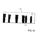
- Fig. 10 is a top plan view of one of the diffraction masks shown in Fig. 9.
- The present invention is directed to a method and apparatus for detecting contaminant particles present on the surface of an object. The invention is based, in part, on the discovery that improved signal to background and signal to noise ratios may be obtained by bringing a beam of light to focus on the surface of the object at a grazing angle and measuring forward scattered light from the surface. Preferably, the forward scattered light is observed at a meridional angle of about 5 to 60 degrees, more preferably at about 30 degrees, and at an azimuthal angle of about 2 to about 10 degrees, more preferably at about 4 degrees. For purposes of the present specification and claims, "meridional angle" is the angle between the plane of incidence of the illumination bean and the observation bean, and "azimuthal angle" is the angle between the observation beam and the surface being inspected.
- Referring now to Fig. 1, there is illustrated an apparatus for detecting particles on a surface of an object, the apparatus being constructed according to the teachings of the present invention and represented generally by reference numeral 11.
- Apparatus 11 includes a
laser 13 for outputting a beam oflaser light 15. Preferably,laser 13 is a 40 mW Nd:YAG laser which produces monochromatic light at 532 nm.Beam 15 is first expanded in cross-section and caused to converge by anexpander 17 and is then deflected by agalvanometer 19 which causes the beam to scan in the y-direction, preferably at a rate of about 50/sec. The beam then passes through an Felens 21 which brings the beam to focus as a small spot or point on astraight scan line 23 on a specimen S, such as a semiconductor wafer or a tile, at a grazing angle a. Grazing angle a is preferably an angle of between about 80 degrees and 90 degrees from the normal to the specimen surface (i.e., between 0 and about 10 degrees from the plane of the specimen surface), more preferably an angle of about 80 degrees from the normal to the specimen surface. - The specimen is mounted on a holder (i.e. stage) 24 which is in the form of a vacuum chuck.
Holder 24 is mounted such that it can be moved in the x-direction so that the entire surface of the specimen can be illuminated, a scan line at a time. Preferably,holder 24 moves at such a speed that the entire surface of the specimen can be illuminated in about 20 seconds. - The light scattered from the specimen is detected by pair of photomultiplier tubes 25-1 and 25-2, which are preferably disposed at a meridional angle of about 30 degrees and at an azimuthal angle of about 4 degrees. The electrical signals outputted by photomultiplier tubes 25 are then fed into a
computer 27 for processing and displayed on adisplay 29. - The entire apparatus 11, except for
computer 27 anddisplay 29, is enclosed within a lighttight housing 31 so that extraneous light is not mistakenly detected. Preferably, the inner walls ofhousing 31 are coated with a dark, non-reflective surface. - As can be appreciated, the meridional angle between the incident beam and the observation beam is not constant over the entire length of the scan line. This is best visualized by referring to Fig. 1 and noting the difference in angles b and c. As discussed above, because certain meridional angles, such as the 30 degree angle, have been found to optimize the signal to background and signal to noise ratios, it is clearthat keeping the meridional angle constant over the length of the scan line is highly desirable.
- Referring now to Figs. 2-8 and in particular to Figs. 2-5, there is illustrated another embodiment of an apparatus for detecting particles on a surface of an object, such as a virgin or patterned semiconductor wafer, ceramic tile, or the like, the apparatus being constructed according to the teachings of the present invention and represented generally by
reference numeral 41. - For the reasons to be discussed below in greater detail,
apparatus 41 solves the problem encountered by apparatus 11 of keeping the meridional angle of observation constant over the entire length of the scan line. -
Apparatus 41 includes a housing 43 (not shown in Fig. 2) which is light tight and whose inner waits are coated with a dark, non-reflective material. Preferably, the dimensions ofhousing 43 are 24 inches in length, 18 inches in width, and 20.5 inches in depth. An optical plate 44 (not shown in Fig. 2), which is also coated with a dark, non-reflective surface, is mounted withinhousing 41 to support some of the optical components to be discussed below. - A
laser 45, which produces an intense beam of collimated light, is disposed withinhousing 43 onplate 44. Preferably,laser 45 is a 40 mW Nd: YAG laser with an output at 532 nm. The beam generated bylaser 45 is passed through a variableneutral density filter 46, which may attenuate the beam, and anexpander 47, whosefirst lens 49 enlarges the cross-sectional diameter of the beam by a magnitude of about 10 and whosesecond lens 51 causes the bean to converge. (Second lens 51 need not be a converging lens; however, by so being, a smaller concave mirror of the type to be discussed below may be used and/or the distance between the concave mirror and the scan line may be reduced.) After emerging fromexpander 47, the beam is deflected off a 45degree mirror 53, which directs the beam to ascanning mirror 55 of agalvanometer 57. Preferably,galvanometer 57 is set so thatmirror 55 scans approximately 50 times per second.Scanning mirror 55 deflects the beam downwardly through a hole inoptical plate 44 where it is deflected off a 45degree mirror 59 disposed at the center of a circle defined by an off-axis hypertelecentric mirror 61. (It is to be understood that the purpose ofmirror 59 is merely to alter the direction of the scanning beam so as to permitapparatus 41 to be reduced in size and thatmirror 59 could be eliminated, as seen in Fig. 5(a), by placingmirror 55 ofgalvanometer 57 wheremirror 59 is shown in Fig. 5.) -
Hypertelecentric mirror 61, which is angled downwardly about 5 degrees, brings the beam deflected bymirror 59 to focus as acurved scan line 89 on a specimen S at a grazing angle of preferably between about 80 and 90 degrees from the normal to the specimen, more preferably at about 80 degrees from the normal to the specimen. - Where, for example,
mirror 59 is disposed at the center of a 1110 mm diameter circle 87 (partially shown in Fig. 5) defined bymirror 61, the light beam comes to focus on the specimen S as anarcuate scan line 89 having a length of about 200 mm and whose nidpoint is about 375 nm frommirror 59. - If specimen S is a patterned object, optimum results are obtained if the light bean strikes the specimen surface at an angle which is not parallel to the direction of the streets of the pattern, but rather, as set forth in U.S. Pat. No. 4,772,126, which issued September 20, 1988 with inventors C.D. Allemand et al., at about a 45 degree angle relative to the pattern streets.
- The light scattered from the specimen S is deflected by a pair of symmetrically disposed mirrors 63-1 and 63-2, which direct the scattered light to respective sets of lenses 65-1 and 65-2 and detectors 67-1 and 67-2. (It is to be understood that mirrors 63-1 and 63-2 are used merely to reduce the size of the apparatus and that they could be eliminated, as seen in Fig. 5(a), by positioning
lenses 65 and/ordetectors 67 where mirrors 63 are currently shown in Fig. 5) For purposes of keeping the meridional angle of observation constant over the scan line, as will be discussed below in greater detail, mirrors 63-1 and 63-2,mirror 59, andarcuate scan line 89 are positioned so that when viewed from directly above they appear to lie along the circumference of animaginary circle 91.Mirrors 63 are disposed at a meridional angle of preferably 5-60 degrees, more preferably 30 degrees, and at an azimuthal angle of preferably 2-10 degrees, more preferably 4 degrees. - As noted above, the light deflected by mirrors 63-1 and 63-2 passes through respective holes in
optical plate 44 and is focused by lenses 65-1 and 65-2, which are preferably 30 mn bi-convex lenses, onto a pair of detectors 67-1 and 67-2. One advantage to using a pair of symmetrically disposed detectors, instead of a single detector, to measure the scattered light is that one can maintain an optimum signal to noise ratio as the illumination bean moves across the scan line. As can readily be appreciated, the intensity of the detected light signal varies as a function of the distance between the detector and that point of the scan line being illuminated. When using only one detector, the variation in the intensity of the light signal as a function of distance can be corrected using computer software; however, because the amount of noise calculated by the computed will itself he dependent upon the signal detected, an optimum signal to noise ratio will not be attained. By way of contrast, if one uses two symmetrically placed detectors, the intensity of the signal will be more constant over the entire scan line, permitting a better signal to noise ratio to be achieved. - Each
detector 67 includes an optical fiber 69, onto which the light focused bylens 65 is imaged, and a photomultiplier tube 71, which is optically coupled to the output of fiber 69. Preferably, the output of fiber 69 and the input of tube 71 are brought into contact with a contact gel (not shown). The reason for using optical fiber 69 rather than imaging the scan line directly onto tube 71 is that the photocathode of tube 71 does not have a uniform response across its surface. Consequently, when the scan line is imaged onto the photocathode, the signal shows up stronger at the center of the photocathode and weaker radially outward. To correct for this lack of uniformity, the scan line is imaged bylens 65 onto fiber 69 which converges it to a small circle (e.g., 8-10 mm) on photomultiplier tube 71. - The outputs from tubes 71 are processed by a
computer 73, which adds the signals using a fixed circuit or which adjusts each signal to account for the possibly different distances from the point of scattering to the respective detectors and then adds the signals. Instead of an addition, an "and" gate could be used for the following reason: Because two photomultiplier tubes are used, the maximum background signal may not appear at the same tine for each photomultiplier tube whereas the maximum particle signal appears simultaneously on both tubes. After processing by the computer, the results are transmitted to adisplay 75. - The specimen is mounted on a
holder 77, which is preferably a vacuum chuck.Holder 77 is mounted on astage 79, which is preferably a telescoping stage to facilitate the mounting and removal of the substrate fromholder 77.Holder 77 is mechanically coupled through a shaft to amotor 81 which causesholder 77 to slide on top ofstage 79 in the direction ofmirror 61. In this way, over a period of about 20 seconds, the entire surface of the specimen can be illuminated, one scan line at a time. If desired,motor 81 may be coupled tocomputer 73 so that the speed at whichholder 77 slides towardsmirror 61 may be adjusted. - Referring now in particular to Fig. 5, a plan view of that portion of
apparatus 41 that is represented byreference numeral 85 in Fig. 3 is shown in order to illustrate how the geometric configuration ofapparatus 41 solves the problem discussed above in connection with apparatus 11, namely, the problem of keeping the meridional angle of observation constant along the entire scan line. As seen by Fig. 5, whenmirror 59, mirrors 63-1 and 63-2, and scanline 89 are viewed from directly above, they appear to be situated on the circumference of animaginary circle 91. (It is to be understood that one or more ofmirror 59, mirrors 63, and scanline 89 may be located on different planes and that whilemirror 59 and mirrors 63-1 and 63-2 are shown in Fig. 5 and referred to herein, mirrors 59 and 63 could be replaced withgalvanometer 57 and/or lenses 65-1 and 65-2, respectively.) Becausemirror 59, mirrors 63, and scanline 89 are thus situated, the meridional angle of observation m for each detector will be the same at every point along the length of the scan line. Moreover, becausemirrors 63 are symmetrically disposed, preferably at about a 30 degree angle relative to mirror 59, the meridional angle of observation m will be the same for both detectors. - Where, for example, the diameter of
circle 87 is 1110 mm and the midpoint ofscan line 89 is about 375 mm frommirror 61, the diameter ofcircle 91 will be approximately 382 mm. - Referring back now to Fig. 2, there can be seen the trapping and masking components of
apparatus 41. The trapping components are used to trap the light that is reflected off, rather than scattered by, the specimen. If the reflected light is not trapped, it might otherwise find its way to the detectors and be picked up as background. In the embodiment shown, the trapping components include atrapping mirror 97 and atrap 99. Trappingmirror 97, which deflects the reflected beam intotrap 99, is preferably placed along the path of the reflected beam at the point where it converges to a point, i.e., at approximately the center of the circle defined bymirror 61.Trap 99 may be a conventional light trap consisting of a multi-walled enclosure which is coated with a dark, non-reflective material. - The masking components for
apparatus 41 are used to minimize the amount of light picked up by the detectors as a result of scattering of the beam bymirror 61. In the embodiment shown, the masking components include ascan line mask 101, a pair of mirror scatter masks 103-1 and 103-2, and four focal masks 105-1 through 105-4.Scan line mask 101 is a curved, dark, non-reflective wall disposed a short distance over the scan line.Mask 101 masks the light scattered bymirror 61 which, if left unmasked, would strike the substrate and possibly be reflected off mirror 63 (see Fig. 6). Mirror scatter masks 103-1 and 103-2, which are flat, dark, non-reflective walls, extend backwards and inwards from either side ofmask 101. Masks 103-1 and 103-2 mask the lightwhich is scattered bymirror 61 directly onto mirror 63 (see Fig. 7). Masks 103-1 and 103-2, however, do not extend so far downwardly that the signal beam becomes masked.Focal masks 105, a pair of which are disposed between eachlens 65 anddetector 67 on the image plane oflens 65, also mask the light which is scattered bymirror 61 directly onto mirror 63 (see Fig. 8). - While
apparatus 41 may be used to detect particles on the surfaces of both virgin and patterned semiconductor wafers, ceramic tiles, and the like, it has been found that illumination of the pattern on patterned objects causes diffraction of the light beam, which may then be detected by detectors 67-1 and 67-2, thereby creating the possibility that an erroneous indication of the presence of a particle may occur. - Referring now to Fig. 9, there is shown an embodiment of an apparatus constructed according to the teachings of the present invention for detecting particles on the surface of a patterned object, such as a semiconductor wafer, ceramic tile, or the like, the apparatus being represented generally by
reference numeral 151. -
Apparatus 151 is similar in construction and operation toapparatus 41, the only difference between the two being thatapparatus 151 additionally includes a pair of identical masks 153-1 and 153-2, mask 153-1 being disposed between mirror 63-1 and lens 65-1 and mask 153-2 being disposed between mirror 63-2 and lens 65-2. As seen in Fig. 10, eachmask 153 preferably comprises atransparent substrate 155, such as a glass slide or the like, onto which are marked one or morenon-transparent bands 157, which correspond to the diffraction pattern created by illumination of the patterned specimen S being examined. As can readily be appreciated, the specific arrangement ofbands 157 onsubstrate 155 will depend upon the particular configuration of the pattern imprinted on the specimen. If the specimen has a narrow pattern imprinted thereon, light will be diffracted at wide angles, and the number ofbands 157 will he comparatively small. In contrast, if the specimen has a wide pattern imprinted thereon, light will be diffracted at narrow angles, and the number ofbands 157 will he comparatively large. - In another embodiment (not shown), detectors 67-1 and 67-2 are replaced with a pair of optical fibers (or with a bifurcated optical fiber) which are optically coupled, preferably through a contact gel, to a single photomultiplier tube.
- Other embodiments (not shown) include substituting an array of photodiodes for the photomultip- tier tubes to avoid the "aging problem" associated with photomultiplier tubes, mounting a pellicle on the concave mirror to keep it clean, using a photomultiplier log amplifier to increase the dynamic range of the photomultiplier, using an L.E.D. lamp lowered to the height of the scan line to check on the long term stability of the detection, using a zener clamp on the dynode network to reduce saturation and recovery time, using a transportation stage wider than the length of the scan line in order to enable observation of wide samples with multiple passes, and using blue light from an argon laser to increase the particle signal.
- The embodiments of the present invention recited herein are intended to be merely exemplary and those skilled in the art will be able to make numerous variations and modifications to it without departing from the spirit of the present invention. All such variations and modifications are intended to be within the scope of the present invention as defined by the claims appended hereto.
Claims (36)
Applications Claiming Priority (2)
| Application Number | Priority Date | Filing Date | Title |
|---|---|---|---|
| US65720791A | 1991-02-19 | 1991-02-19 | |
| US657207 | 1991-02-19 |
Publications (3)
| Publication Number | Publication Date |
|---|---|
| EP0500293A2 true EP0500293A2 (en) | 1992-08-26 |
| EP0500293A3 EP0500293A3 (en) | 1993-01-20 |
| EP0500293B1 EP0500293B1 (en) | 1997-05-07 |
Family
ID=24636256
Family Applications (1)
| Application Number | Title | Priority Date | Filing Date |
|---|---|---|---|
| EP92301275A Expired - Lifetime EP0500293B1 (en) | 1991-02-19 | 1992-02-17 | Particle detection method and apparatus |
Country Status (4)
| Country | Link |
|---|---|
| US (1) | US5317380A (en) |
| EP (1) | EP0500293B1 (en) |
| AT (1) | ATE152827T1 (en) |
| DE (1) | DE69219501T2 (en) |
Cited By (3)
| Publication number | Priority date | Publication date | Assignee | Title |
|---|---|---|---|---|
| US6486946B1 (en) | 1999-06-15 | 2002-11-26 | Ade Corporation | Method for discriminating between holes in and particles on a film covering a substrate |
| WO2015184086A1 (en) * | 2014-05-29 | 2015-12-03 | Corning Incorporated | Method for particle detection on flexible substrates |
| CN106323988A (en) * | 2016-08-19 | 2017-01-11 | 桐乡市嘉乐玻璃马赛克有限公司 | Mosaic tile needle hole detecting device |
Families Citing this family (52)
| Publication number | Priority date | Publication date | Assignee | Title |
|---|---|---|---|---|
| JP3271425B2 (en) * | 1994-03-30 | 2002-04-02 | ソニー株式会社 | Foreign matter inspection device and foreign matter inspection method |
| US5883710A (en) * | 1994-12-08 | 1999-03-16 | Kla-Tencor Corporation | Scanning system for inspecting anomalies on surfaces |
| US5864394A (en) * | 1994-06-20 | 1999-01-26 | Kla-Tencor Corporation | Surface inspection system |
| US20040057044A1 (en) * | 1994-12-08 | 2004-03-25 | Mehrdad Nikoonahad | Scanning system for inspecting anamolies on surfaces |
| JPH08178857A (en) * | 1994-12-21 | 1996-07-12 | Nikon Corp | Foreign matter inspection device for large substrate |
| US5631733A (en) * | 1995-01-20 | 1997-05-20 | Photon Dynamics, Inc. | Large area defect monitor tool for manufacture of clean surfaces |
| US5653537A (en) * | 1995-03-17 | 1997-08-05 | Ircon, Inc. | Non-contacting infrared temperature thermometer detector apparatus |
| US5604585A (en) * | 1995-03-31 | 1997-02-18 | Tencor Instruments | Particle detection system employing a subsystem for collecting scattered light from the particles |
| US5982500A (en) * | 1995-05-07 | 1999-11-09 | Platsch; Hans Georg | Device for measuring the surface of a print product |
| US5649169A (en) * | 1995-06-20 | 1997-07-15 | Advanced Micro Devices, Inc. | Method and system for declustering semiconductor defect data |
| US5539752A (en) * | 1995-06-30 | 1996-07-23 | Advanced Micro Devices, Inc. | Method and system for automated analysis of semiconductor defect data |
| US5742422A (en) * | 1995-09-19 | 1998-04-21 | Inspex, Inc. | Adjustable fourier mask |
| US5825482A (en) * | 1995-09-29 | 1998-10-20 | Kla-Tencor Corporation | Surface inspection system with misregistration error correction and adaptive illumination |
| US5777901A (en) * | 1995-09-29 | 1998-07-07 | Advanced Micro Devices, Inc. | Method and system for automated die yield prediction in semiconductor manufacturing |
| US5913105A (en) * | 1995-11-29 | 1999-06-15 | Advanced Micro Devices Inc | Method and system for recognizing scratch patterns on semiconductor wafers |
| JP4306800B2 (en) * | 1996-06-04 | 2009-08-05 | ケーエルエー−テンカー テクノロジィース コーポレイション | Optical scanning system for surface inspection |
| US5801824A (en) * | 1996-11-25 | 1998-09-01 | Photon Dynamics, Inc. | Large area defect monitor tool for manufacture of clean surfaces |
| EP1016126B1 (en) * | 1997-03-31 | 2018-12-26 | Nanometrics Incorporated | Optical inspection module and method for detecting particles and defects on substrates in integrated process tools |
| US5745239A (en) * | 1997-04-07 | 1998-04-28 | Taiwan Semiconductor Manufacturing Company | Multiple focal plane image comparison for defect detection and classification |
| US5933230A (en) * | 1997-04-28 | 1999-08-03 | International Business Machines Corporation | Surface inspection tool |
| US5867261A (en) * | 1997-04-28 | 1999-02-02 | International Business Machines Corporation | Surface inspection tool |
| US5917589A (en) * | 1997-04-28 | 1999-06-29 | International Business Machines Corporation | Surface inspection tool |
| US6073501A (en) * | 1997-06-20 | 2000-06-13 | Advanced Micro Devices, Inc. | Apparatus and method for semiconductor wafer processing which facilitate determination of a source of contaminants or defects |
| US5812270A (en) * | 1997-09-17 | 1998-09-22 | Ircon, Inc. | Window contamination detector |
| ATE282590T1 (en) | 1998-05-15 | 2004-12-15 | Astrazeneca Ab | BENZAMIDE DERIVATIVES FOR THE TREATMENT OF CYTOKINE-MEDIATED DISEASES |
| US6879391B1 (en) | 1999-05-26 | 2005-04-12 | Kla-Tencor Technologies | Particle detection method and apparatus |
| US7349090B2 (en) | 2000-09-20 | 2008-03-25 | Kla-Tencor Technologies Corp. | Methods and systems for determining a property of a specimen prior to, during, or subsequent to lithography |
| US6891627B1 (en) | 2000-09-20 | 2005-05-10 | Kla-Tencor Technologies Corp. | Methods and systems for determining a critical dimension and overlay of a specimen |
| EP1319244A1 (en) * | 2000-09-20 | 2003-06-18 | Kla-Tencor Inc. | Methods and systems for semiconductor fabrication processes |
| WO2002040970A1 (en) | 2000-11-15 | 2002-05-23 | Real Time Metrology, Inc. | Optical method and apparatus for inspecting large area planar objects |
| US6809809B2 (en) * | 2000-11-15 | 2004-10-26 | Real Time Metrology, Inc. | Optical method and apparatus for inspecting large area planar objects |
| US7072034B2 (en) * | 2001-06-08 | 2006-07-04 | Kla-Tencor Corporation | Systems and methods for inspection of specimen surfaces |
| US6538730B2 (en) * | 2001-04-06 | 2003-03-25 | Kla-Tencor Technologies Corporation | Defect detection system |
| EP1393115B1 (en) | 2001-05-03 | 2011-11-30 | KLA-Tencor Technologies Corporation | Systems and methods for scanning a beam of light across a specimen |
| US6922236B2 (en) | 2001-07-10 | 2005-07-26 | Kla-Tencor Technologies Corp. | Systems and methods for simultaneous or sequential multi-perspective specimen defect inspection |
| US6778267B2 (en) | 2001-09-24 | 2004-08-17 | Kla-Tencor Technologies Corp. | Systems and methods for forming an image of a specimen at an oblique viewing angle |
| US20040032581A1 (en) * | 2002-01-15 | 2004-02-19 | Mehrdad Nikoonahad | Systems and methods for inspection of specimen surfaces |
| KR100493847B1 (en) * | 2003-04-09 | 2005-06-08 | 삼성전자주식회사 | Method and apparatus for detecting a particle |
| US7078712B2 (en) * | 2004-03-18 | 2006-07-18 | Axcelis Technologies, Inc. | In-situ monitoring on an ion implanter |
| JP4593243B2 (en) * | 2004-11-18 | 2010-12-08 | 株式会社トプコン | Air particle monitoring device and vacuum processing device |
| WO2007061383A1 (en) * | 2005-11-25 | 2007-05-31 | Agency For Science, Technology & Research | Determination of field distribution |
| JP4876019B2 (en) * | 2007-04-25 | 2012-02-15 | 株式会社日立ハイテクノロジーズ | Defect inspection apparatus and method |
| US7767982B2 (en) * | 2007-06-06 | 2010-08-03 | Hermes-Microvision, Inc. | Optical auto focusing system and method for electron beam inspection tool |
| JP2009002733A (en) * | 2007-06-20 | 2009-01-08 | Toshiba Corp | Suspended particle detection device and suspended particle detection method |
| US20090002686A1 (en) * | 2007-06-29 | 2009-01-01 | The Material Works, Ltd. | Sheet Metal Oxide Detector |
| CN102645437A (en) * | 2012-04-11 | 2012-08-22 | 法国圣戈班玻璃公司 | Optical measurement device and optical measurement method |
| US9395340B2 (en) | 2013-03-15 | 2016-07-19 | Kla-Tencor Corporation | Interleaved acousto-optical device scanning for suppression of optical crosstalk |
| US9599572B2 (en) * | 2014-04-07 | 2017-03-21 | Orbotech Ltd. | Optical inspection system and method |
| CN113702269B (en) * | 2016-01-21 | 2024-04-09 | 东京毅力科创株式会社 | Chemical liquid supply device and coating and developing system |
| CN106352960B (en) * | 2016-08-16 | 2018-11-06 | 黄阳 | A kind of mosaic tiles Weight detecting device |
| FR3056295B1 (en) * | 2016-09-21 | 2018-09-14 | Constellium Neuf Brisach | DEVICE FOR DETECTING SURFACE DEFECTS OF ALUMINUM LAMINATED BANDS |
| CN107421916B (en) * | 2017-05-02 | 2021-02-23 | 京东方科技集团股份有限公司 | Detection device, process system and detection method |
Citations (5)
| Publication number | Priority date | Publication date | Assignee | Title |
|---|---|---|---|---|
| US4669875A (en) * | 1982-11-04 | 1987-06-02 | Hitachi, Ltd. | Foreign particle detecting method and apparatus |
| JPS62124447A (en) * | 1985-11-25 | 1987-06-05 | Canon Inc | Surface state measuring instrument |
| US4812664A (en) * | 1987-11-12 | 1989-03-14 | High Yield Technology | Apparatus for scanning a flat surface to detect defects |
| US4898471A (en) * | 1987-06-18 | 1990-02-06 | Tencor Instruments | Particle detection on patterned wafers and the like |
| EP0398781A2 (en) * | 1989-05-19 | 1990-11-22 | Eastman Kodak Company | Method and apparatus for low angle, high resolution surface inspection |
Family Cites Families (11)
| Publication number | Priority date | Publication date | Assignee | Title |
|---|---|---|---|---|
| US2947212A (en) * | 1956-04-30 | 1960-08-02 | American Brass Co | Method of detecting surface conditions of sheet metal |
| US3782836A (en) * | 1971-11-11 | 1974-01-01 | Texas Instruments Inc | Surface irregularity analyzing method |
| US4342515A (en) * | 1978-01-27 | 1982-08-03 | Hitachi, Ltd. | Method of inspecting the surface of an object and apparatus therefor |
| US4337340A (en) * | 1979-06-14 | 1982-06-29 | Sterling Drug Inc. | Processes for preparing substituted furopyridinones and furopyrazinones |
| US4468120A (en) * | 1981-02-04 | 1984-08-28 | Nippon Kogaku K.K. | Foreign substance inspecting apparatus |
| JPS61162738A (en) * | 1985-01-11 | 1986-07-23 | Hitachi Ltd | Inspection of foreign matter |
| JPH0727125B2 (en) * | 1986-05-23 | 1995-03-29 | 株式会社日立製作所 | Optical scanning device |
| US4772126A (en) * | 1986-10-23 | 1988-09-20 | Inspex Incorporated | Particle detection method and apparatus |
| US4889998A (en) * | 1987-01-29 | 1989-12-26 | Nikon Corporation | Apparatus with four light detectors for checking surface of mask with pellicle |
| JPH0820371B2 (en) * | 1988-01-21 | 1996-03-04 | 株式会社ニコン | Defect inspection device and defect inspection method |
| US5076692A (en) * | 1990-05-31 | 1991-12-31 | Tencor Instruments | Particle detection on a patterned or bare wafer surface |
-
1991
- 1991-12-31 US US07/815,145 patent/US5317380A/en not_active Expired - Lifetime
-
1992
- 1992-02-17 AT AT92301275T patent/ATE152827T1/en not_active IP Right Cessation
- 1992-02-17 EP EP92301275A patent/EP0500293B1/en not_active Expired - Lifetime
- 1992-02-17 DE DE69219501T patent/DE69219501T2/en not_active Expired - Lifetime
Patent Citations (5)
| Publication number | Priority date | Publication date | Assignee | Title |
|---|---|---|---|---|
| US4669875A (en) * | 1982-11-04 | 1987-06-02 | Hitachi, Ltd. | Foreign particle detecting method and apparatus |
| JPS62124447A (en) * | 1985-11-25 | 1987-06-05 | Canon Inc | Surface state measuring instrument |
| US4898471A (en) * | 1987-06-18 | 1990-02-06 | Tencor Instruments | Particle detection on patterned wafers and the like |
| US4812664A (en) * | 1987-11-12 | 1989-03-14 | High Yield Technology | Apparatus for scanning a flat surface to detect defects |
| EP0398781A2 (en) * | 1989-05-19 | 1990-11-22 | Eastman Kodak Company | Method and apparatus for low angle, high resolution surface inspection |
Non-Patent Citations (1)
| Title |
|---|
| PATENT ABSTRACTS OF JAPAN vol. 11, no. 340 (P-634)7 November 1987 & JP-A-62 124 447 ( CANON INC ) 5 June 1987 * |
Cited By (5)
| Publication number | Priority date | Publication date | Assignee | Title |
|---|---|---|---|---|
| US6486946B1 (en) | 1999-06-15 | 2002-11-26 | Ade Corporation | Method for discriminating between holes in and particles on a film covering a substrate |
| WO2015184086A1 (en) * | 2014-05-29 | 2015-12-03 | Corning Incorporated | Method for particle detection on flexible substrates |
| CN106461571A (en) * | 2014-05-29 | 2017-02-22 | 康宁股份有限公司 | Method for particle detection on flexible substrates |
| CN106323988A (en) * | 2016-08-19 | 2017-01-11 | 桐乡市嘉乐玻璃马赛克有限公司 | Mosaic tile needle hole detecting device |
| CN106323988B (en) * | 2016-08-19 | 2018-10-23 | 泉州台商投资区五季网络有限公司 | A kind of mosaic tiles Pinhole detecting device |
Also Published As
| Publication number | Publication date |
|---|---|
| EP0500293A3 (en) | 1993-01-20 |
| US5317380A (en) | 1994-05-31 |
| DE69219501T2 (en) | 1998-01-02 |
| EP0500293B1 (en) | 1997-05-07 |
| ATE152827T1 (en) | 1997-05-15 |
| DE69219501D1 (en) | 1997-06-12 |
Similar Documents
| Publication | Publication Date | Title |
|---|---|---|
| EP0500293B1 (en) | Particle detection method and apparatus | |
| US4895446A (en) | Particle detection method and apparatus | |
| US5805278A (en) | Particle detection method and apparatus | |
| US5659390A (en) | Method and apparatus for detecting particles on a surface of a semiconductor wafer having repetitive patterns | |
| US4772126A (en) | Particle detection method and apparatus | |
| US7016526B2 (en) | Pixel based machine for patterned wafers | |
| US4655592A (en) | Particle detection method and apparatus | |
| US6956644B2 (en) | Systems and methods for a wafer inspection system using multiple angles and multiple wavelength illumination | |
| US4597665A (en) | Dual collector optical flaw detector | |
| US7369223B2 (en) | Method of apparatus for detecting particles on a specimen | |
| US4898471A (en) | Particle detection on patterned wafers and the like | |
| JP4183492B2 (en) | Defect inspection apparatus and defect inspection method | |
| JPS6182147A (en) | Method and device for inspecting surface | |
| US6496256B1 (en) | Inspection systems using sensor array and double threshold arrangement | |
| US6208750B1 (en) | Method for detecting particles using illumination with several wavelengths | |
| KR20070107773A (en) | Method and apparatus for detecting and/or classifying defects | |
| JP2008096430A (en) | Method and apparatus for detecting defect | |
| EP1938273A2 (en) | Device and method for inspecting an object | |
| JP2999712B2 (en) | Edge defect inspection method and apparatus | |
| WO1996005503A1 (en) | Device for testing optical elements | |
| CA2282015C (en) | Light-scanning device | |
| JP3338118B2 (en) | Method for manufacturing semiconductor device | |
| JPS61207951A (en) | Defect inspecting device for transparent object | |
| JPH05215690A (en) | Inspecting apparatus for foreign matter | |
| JPS6256847A (en) | Surface inspecting equipment using light beam |
Legal Events
| Date | Code | Title | Description |
|---|---|---|---|
| PUAI | Public reference made under article 153(3) epc to a published international application that has entered the european phase |
Free format text: ORIGINAL CODE: 0009012 |
|
| AK | Designated contracting states |
Kind code of ref document: A2 Designated state(s): AT BE CH DE DK ES FR GB GR IT LI LU MC NL PT SE |
|
| PUAL | Search report despatched |
Free format text: ORIGINAL CODE: 0009013 |
|
| AK | Designated contracting states |
Kind code of ref document: A3 Designated state(s): AT BE CH DE DK ES FR GB GR IT LI LU MC NL PT SE |
|
| 17P | Request for examination filed |
Effective date: 19930714 |
|
| 17Q | First examination report despatched |
Effective date: 19950816 |
|
| GRAG | Despatch of communication of intention to grant |
Free format text: ORIGINAL CODE: EPIDOS AGRA |
|
| GRAH | Despatch of communication of intention to grant a patent |
Free format text: ORIGINAL CODE: EPIDOS IGRA |
|
| GRAH | Despatch of communication of intention to grant a patent |
Free format text: ORIGINAL CODE: EPIDOS IGRA |
|
| GRAA | (expected) grant |
Free format text: ORIGINAL CODE: 0009210 |
|
| AK | Designated contracting states |
Kind code of ref document: B1 Designated state(s): AT BE CH DE DK ES FR GB GR IT LI LU MC NL PT SE |
|
| PG25 | Lapsed in a contracting state [announced via postgrant information from national office to epo] |
Ref country code: DK Effective date: 19970507 Ref country code: IT Free format text: LAPSE BECAUSE OF FAILURE TO SUBMIT A TRANSLATION OF THE DESCRIPTION OR TO PAY THE FEE WITHIN THE PRE;WARNING: LAPSES OF ITALIAN PATENTS WITH EFFECTIVE DATE BEFORE 2007 MAY HAVE OCCURRED AT ANY TIME BEFORE 2007. THE CORRECT EFFECTIVE DATE MAY BE DIFFERENT FROM THE ONE RECORDED.SCRIBED TIME-LIMIT Effective date: 19970507 Ref country code: GR Free format text: LAPSE BECAUSE OF FAILURE TO SUBMIT A TRANSLATION OF THE DESCRIPTION OR TO PAY THE FEE WITHIN THE PRESCRIBED TIME-LIMIT Effective date: 19970507 Ref country code: ES Free format text: THE PATENT HAS BEEN ANNULLED BY A DECISION OF A NATIONAL AUTHORITY Effective date: 19970507 Ref country code: NL Free format text: LAPSE BECAUSE OF FAILURE TO SUBMIT A TRANSLATION OF THE DESCRIPTION OR TO PAY THE FEE WITHIN THE PRESCRIBED TIME-LIMIT Effective date: 19970507 Ref country code: CH Effective date: 19970507 Ref country code: AT Effective date: 19970507 Ref country code: FR Effective date: 19970507 Ref country code: BE Effective date: 19970507 Ref country code: LI Effective date: 19970507 |
|
| REF | Corresponds to: |
Ref document number: 152827 Country of ref document: AT Date of ref document: 19970515 Kind code of ref document: T |
|
| REG | Reference to a national code |
Ref country code: CH Ref legal event code: EP |
|
| REF | Corresponds to: |
Ref document number: 69219501 Country of ref document: DE Date of ref document: 19970612 |
|
| PG25 | Lapsed in a contracting state [announced via postgrant information from national office to epo] |
Ref country code: PT Effective date: 19970807 Ref country code: SE Effective date: 19970807 |
|
| NLV1 | Nl: lapsed or annulled due to failure to fulfill the requirements of art. 29p and 29m of the patents act | ||
| EN | Fr: translation not filed | ||
| REG | Reference to a national code |
Ref country code: CH Ref legal event code: PL |
|
| PG25 | Lapsed in a contracting state [announced via postgrant information from national office to epo] |
Ref country code: LU Free format text: LAPSE BECAUSE OF NON-PAYMENT OF DUE FEES Effective date: 19980217 |
|
| PLBE | No opposition filed within time limit |
Free format text: ORIGINAL CODE: 0009261 |
|
| STAA | Information on the status of an ep patent application or granted ep patent |
Free format text: STATUS: NO OPPOSITION FILED WITHIN TIME LIMIT |
|
| 26N | No opposition filed | ||
| PG25 | Lapsed in a contracting state [announced via postgrant information from national office to epo] |
Ref country code: MC Free format text: LAPSE BECAUSE OF NON-PAYMENT OF DUE FEES Effective date: 19980831 |
|
| REG | Reference to a national code |
Ref country code: GB Ref legal event code: IF02 |
|
| PGFP | Annual fee paid to national office [announced via postgrant information from national office to epo] |
Ref country code: GB Payment date: 20080227 Year of fee payment: 17 |
|
| GBPC | Gb: european patent ceased through non-payment of renewal fee |
Effective date: 20090217 |
|
| PG25 | Lapsed in a contracting state [announced via postgrant information from national office to epo] |
Ref country code: GB Free format text: LAPSE BECAUSE OF NON-PAYMENT OF DUE FEES Effective date: 20090217 |
|
| PGFP | Annual fee paid to national office [announced via postgrant information from national office to epo] |
Ref country code: DE Payment date: 20110225 Year of fee payment: 20 |
|
| REG | Reference to a national code |
Ref country code: DE Ref legal event code: R071 Ref document number: 69219501 Country of ref document: DE |
|
| REG | Reference to a national code |
Ref country code: DE Ref legal event code: R071 Ref document number: 69219501 Country of ref document: DE |
|
| PG25 | Lapsed in a contracting state [announced via postgrant information from national office to epo] |
Ref country code: DE Free format text: LAPSE BECAUSE OF EXPIRATION OF PROTECTION Effective date: 20120218 |
|
| P01 | Opt-out of the competence of the unified patent court (upc) registered |
Effective date: 20230525 |