EP0501220A2 - Process for manufacturing DC superconducting quantum interference device - Google Patents
Process for manufacturing DC superconducting quantum interference device Download PDFInfo
- Publication number
- EP0501220A2 EP0501220A2 EP92102267A EP92102267A EP0501220A2 EP 0501220 A2 EP0501220 A2 EP 0501220A2 EP 92102267 A EP92102267 A EP 92102267A EP 92102267 A EP92102267 A EP 92102267A EP 0501220 A2 EP0501220 A2 EP 0501220A2
- Authority
- EP
- European Patent Office
- Prior art keywords
- coil
- steps
- washer
- deposited
- input
- Prior art date
- Legal status (The legal status is an assumption and is not a legal conclusion. Google has not performed a legal analysis and makes no representation as to the accuracy of the status listed.)
- Granted
Links
Images


Classifications
-
- H—ELECTRICITY
- H10—SEMICONDUCTOR DEVICES; ELECTRIC SOLID-STATE DEVICES NOT OTHERWISE PROVIDED FOR
- H10N—ELECTRIC SOLID-STATE DEVICES NOT OTHERWISE PROVIDED FOR
- H10N60/00—Superconducting devices
- H10N60/01—Manufacture or treatment
- H10N60/0912—Manufacture or treatment of Josephson-effect devices
-
- Y—GENERAL TAGGING OF NEW TECHNOLOGICAL DEVELOPMENTS; GENERAL TAGGING OF CROSS-SECTIONAL TECHNOLOGIES SPANNING OVER SEVERAL SECTIONS OF THE IPC; TECHNICAL SUBJECTS COVERED BY FORMER USPC CROSS-REFERENCE ART COLLECTIONS [XRACs] AND DIGESTS
- Y10—TECHNICAL SUBJECTS COVERED BY FORMER USPC
- Y10S—TECHNICAL SUBJECTS COVERED BY FORMER USPC CROSS-REFERENCE ART COLLECTIONS [XRACs] AND DIGESTS
- Y10S505/00—Superconductor technology: apparatus, material, process
- Y10S505/80—Material per se process of making same
- Y10S505/815—Process of making per se
- Y10S505/816—Sputtering, including coating, forming, or etching
- Y10S505/817—Sputtering, including coating, forming, or etching forming josephson element
-
- Y—GENERAL TAGGING OF NEW TECHNOLOGICAL DEVELOPMENTS; GENERAL TAGGING OF CROSS-SECTIONAL TECHNOLOGIES SPANNING OVER SEVERAL SECTIONS OF THE IPC; TECHNICAL SUBJECTS COVERED BY FORMER USPC CROSS-REFERENCE ART COLLECTIONS [XRACs] AND DIGESTS
- Y10—TECHNICAL SUBJECTS COVERED BY FORMER USPC
- Y10S—TECHNICAL SUBJECTS COVERED BY FORMER USPC CROSS-REFERENCE ART COLLECTIONS [XRACs] AND DIGESTS
- Y10S505/00—Superconductor technology: apparatus, material, process
- Y10S505/825—Apparatus per se, device per se, or process of making or operating same
- Y10S505/831—Static information storage system or device
- Y10S505/832—Josephson junction type
-
- Y—GENERAL TAGGING OF NEW TECHNOLOGICAL DEVELOPMENTS; GENERAL TAGGING OF CROSS-SECTIONAL TECHNOLOGIES SPANNING OVER SEVERAL SECTIONS OF THE IPC; TECHNICAL SUBJECTS COVERED BY FORMER USPC CROSS-REFERENCE ART COLLECTIONS [XRACs] AND DIGESTS
- Y10—TECHNICAL SUBJECTS COVERED BY FORMER USPC
- Y10S—TECHNICAL SUBJECTS COVERED BY FORMER USPC CROSS-REFERENCE ART COLLECTIONS [XRACs] AND DIGESTS
- Y10S505/00—Superconductor technology: apparatus, material, process
- Y10S505/825—Apparatus per se, device per se, or process of making or operating same
- Y10S505/842—Measuring and testing
- Y10S505/843—Electrical
- Y10S505/845—Magnetometer
- Y10S505/846—Magnetometer using superconductive quantum interference device, i.e. squid
Definitions
- the present invention relates to a process for manufacturing a DC superconducting quantum interference device (which will be shortly referred to as "DC-SQUID”), which is applied to a highly sensitive magnetic sensor, an ammeter, a displacement meter, a high-frequency signal amplifier or the like.
- DC-SQUID DC superconducting quantum interference device
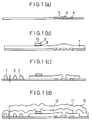
- Figs. 2(a) to 2(e) The steps of the prior art are shown in sections in Figs. 2(a) to 2(e). These steps manufacture a SQUID integrated with a pick-up coil and begin fabricating a pick-up coil 1, a feedback coil 2 and an input coil 3 before the remaining steps.
- the individual steps will be briefly described in the following.
- Fig. 2(a) shows a step at which the surface is flattened with the first insulating film 4 after the pick-up coil 1, the feedback coil 2 and the input coil 3 are formed of a superconducting film.
- This superconducting film is formed by depositing Nb by a sputtering, and the first insulating film 4 is flattened by applying SOG after SiO2 has been deposited by a plasma CVD.
- Fig. 2(b) shows a step at which a resistance film 5 for shunting or damping the SQUID is set to a designed value by a second insulating film 6 after it has been deposited.
- the resistance film 5 is made of Pd, and the second insulating film 5 is formed by evaporating MgO together.
- Fig. 2(c) and 2(d) show steps at which a Josephson junction 10 and a washer coil 11 are fabricated.
- the Josephson junction 10 is deposited a Nb/A l -oxide/Nb structure by a sputtering.
- the washer coil 11 is formed of a lower electrode 7 of the Josephson junction 10.
- Fig. 2(e) shows a step at which an opposed electrode 13 of a superconducting film is formed after a third insulating film 12 has been deposited.
- the third insulating film 12 and the counter electrode 13 are deposited together, respectively, by evaporating SiO and PbIn.
- the pick-up coil 1, the feedback coil 2 and the input coil 3 are fabricated before the remaining steps so that the number of masks for patterning the deposited films by a photolithography increases. Since the number of steps increases, the time for the manufacture is elongated to reduce the production yield of the element.
- the feedback coil and the input coil are isotropically etched to have a tapered pattern thereby to eliminate the flattening step by the SOG.
- at least one of the Josephson element and the counter electrode is fabricated simultaneously with the step of fabricating the input coil and the feedback coil.
- the number of masks is reduced by the above-specified process, the number of steps can be reduced to manufacture a magnetic field detector having improved production yield and characteristics.
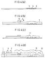
- Figs. 1(a) to 1(d) are sectional views showing the steps of a first embodiment of the present invention.
- Figs. 2(a) to 2(e) are sectional views showing the steps of the prior art.
- Fig. 3 is a top plan view showing the first embodiment of the present invention.
- Figs. 4(a) to 4(d) are sectional views showing the steps of a second embodiment of the present invention.
- Fig. 5 is a top plan view showing the second embodiment of the present invention.
- Figs. 6(a) to 6(d) are sectional views showing the steps of a third embodiment of the present invention.
- Figs. 7(a) to 7(d) are sectional views showing the steps of a fourth embodiment of the present invention.
- Fig. 8 is a top plan view of a DC-SQUID having double-washer coils connected in series.
- Fig. 9 is a top plan view of a DC-SQUID having double-washer coils connected in parallel.
- Fig. 10 is a top plan view showing a gradiometer DC-SQUID.
- FIG. 3 is a top plan view showing a first embodiment of the present invention.
- Figs. 1(a) to 1(d) are sections taken along line A - A' of Fig. 3 and showing the steps. The manufacture process will be described with reference to Figs. 1(a) to 1(d).
- Fig 1(a) shows a step at which a resistance film 5 for shunting or damping a DC-SQUID is insulated by a second insulating film 6 to have a designed resistance after it has been deposited.
- the resistance film 5 can be made of a metal such as Mo, MoN, Pd, Au, Cu, A l or Pd, any of which can be deposited by a sputtering or evaporation.
- the Mo is deposited to a thickness of 100 nm by a DC magnetron sputtering and is patterned to a designed size at a photolithographic step.
- the second insulating film 6 can be made of SiO2, SiO, Si or MgO. Any of these materials can be deposited by the sputtering, evaporation or CVD.
- the deposited film is set to be 1.5 to 2 times as thick as the resistance film 5 so as to insulate the resistance film 5 completely.
- the SiO2 is deposited to 150 to 200 nm by an RF magnetron sputtering and is enabled to contact with the resistance film 5 by the photolithographic step.
- Both the wet and dray etching methods can be used for etching the SiO2.
- the wet etching is exemplified by a method using a mixture of hydrofluoric acid.
- the dry etching is exemplified by a reactive ion etching (i.e., RIE) using a mixture of CF4 or CHF3 and oxygen.
- RIE reactive ion etching
- the SiO2 is etched by the RIE using the mixture of CHF3 and oxygen.
- Fig. 1(d) shows a step for fabricating a Josephson junction 10, at which a lower electrode 7, a barrier layer 8 and an upper electrode 9 are deposited and at which the upper electrode 9 and the barrier layer 8 are etching by the photolithography.
- the Josephson junction 10 can be exemplified not only by the Nb/A l -oxide structure but also by a variety of structures of NbN/MgO/NbN, Nb/Si/Nb, Nb/Nb-oxed/Nb.
- the Nb/A l -oxide/Nb structure is deposited by the sputtering. Examples of the deposition are as follows.
- An argon gas is introduced into a reaction chamber, which is evacuated to a high vacuum of 10 ⁇ 5 Pa or less, and the Nb film of the lower electrode 7 is deposited under a pressure of 0.2 to 4 Pa by the DC magnetron sputtering.
- the film is set to be about 1.5 to 2 times as thick as the second insulating film 6 and is deposited to 200 to 300 nm.
- the introduction of the argon gas is interrupted, and the reaction chamber is evacuated to a high vacuum of 10 ⁇ 5 Pa or less.
- the argon gas is introduced so that the A l is deposited to 1 to 20 nm under a pressure of 0.2 to 4 Pa by the DC magnetron sputtering.
- the reaction chamber is evacuated to a high vacuum of 10 ⁇ 5 Pa or less, and an oxygen gas or a mixture of oxygen and argon is introduced to adjust the pressure to the set level. Then, the A l surface is oxidized to form the barrier layer 8 of A l Ox/A l .
- the reaction chamber is evacuated to a high vacuum of 10 ⁇ 5 Pa or less, and the upper electrode 9 is deposited to 100 to 300 nm under the aforementioned Nb depositing condition. Next, the upper electrode 9 and the barrier layer 8 are etching at the photolithographic step to form the Josephson junction 10.
- the etching method used is generally the dry etching method using a plasma.
- the Nb of the upper electrode 9 is subjected to the reactive ion etching (i.e., RIE) using CF4 or a mixture of CF4 and oxygen.
- the A l of the barrier layer 8 is removed by either the wet etching method using an acid or the RIE using an Ar gas.
- the barrier layer 8 need not be etched.
- Fig. 1(c) shows a step, at which a detection coil 1, a feedback modulation coil 2 and an input coil 3 are formed by patterning the superconducting film deposited as the lower electrode 7 of the Josephson junction 10 by the photolithography.
- the etching method used is generally the dry etching method using plasma.
- the Nb of the lower electrode 7 is subjected to the plasma etching or reactive ion etching (i.e., RIE) using a mixture of CF4 and oxygen.
- the etching is so different from that of the aforementioned upper electrode 9 that the isotropic etching is effected by increasing the amount of oxygen and that the resist film in the peripheral of the pattern is etched with the oxygen into a tapered shape.
- the etching can be specifically exemplified by using the plasma etching apparatus with a gas, which is prepared by adding 10 % of oxygen to the CF4, under a pressure of 133 Pa and with a power of 50 W.
- Fig. 1(d) shows a step, at which: a third insulating film 12 or an inter-layer insulating film is deposited; a contact hole is then formed by the photolithography; and a superconducting film is then deposited to form a washer coil 11 and an electrode 13 by the photolithography.
- the third insulating film 12 can be deposited by a method similar to that of the second insulating film 6.
- the SiO2 is deposited to 300 to 500 nm by the RF magnetron sputtering, and the contact hole is formed by the photolithography.
- the etching of the SiO2 is performed by the RIE like the second insulating film 6.
- the superconducting film is exemplified by the Nb, NbN, Pb-In or Pn-In-Au which is deposited by the sputtering or evaporation.
- the Nb film is deposited to 400 to 600 nm by the DC magnetron sputtering like the electrode of the Josephson junction.
- the substrate is inversely sputtered with the Ar gas so as to form the superconducting contact.
- the washer coil 11, the counter electrode 13 and other wiring portions are formed by the photolithography.
- the etching is exemplified by the plasma etching like the aforementioned lower electrode 7.
- Fig. 5 is a top plan view showing a second embodiment of the present invention, from which the pick-up coil 1 is omitted.
- Fig. 4 is a section taken along line A - A' of Fig. 5. This method fabricates the counter electrode 13 simultaneously with the pick-up coil 1, the feedback coil 2 and the input coil 3, and the methods of fabricating the individual layers are similar to those of the first embodiment.
- Fig. 6 presents sections showing the steps of a third embodiment. This manufacture process is different from the foregoing two embodiments in the method of forming the Josephson junction 10 such that the upper electrode 9 is formed after the etching has been performed beforehand up to the lower electrode 7. (Figs. 6(b) and 6(c)) At this step, the second insulating film 6 has to be left unetched at the time of etching the upper electrode 9. In case the second insulating film used is made of SiO2, SiO or Si, its surface is covered with A l , and oxide film of A l or MgO so that it may not be etched.
- Fig. 6 corresponds to the first embodiment of Fig. 1 but can also be applied to the second embodiment if the pick-up coil 1, the feedback coil 2 and the input coil 3 are fabricated at steps similar to those of the second embodiment.
- Fig. 7 presents sections showing the steps of a fourth embodiment.
- This embodiment is a process for self-aligning the third insulating film 12 at a lift-off step. Specifically, the upper electrode 9 is etched by the RIE by using a photoresist as a mask, and the SiO is deposited by the evaporation and lifted off. Since the fourth embodiment is dispensed with the photolithography step for forming the contact hole in the third insulating film, the number of masks is further reduced to provide a manufacture process having less steps.
- the last layer need not be tapered but may be patterned at the lift-off step.
- the resistance film 5 is fabricated at first but may be fabricated after the Josephson junction 10 has been fabricated. Since the pick-up coil 1 can be fabricated independently of other steps, it need not be fabricated together with the feedback coil 2 and the input coil 3. Moreover, they can be fabricated integrally in a common plane and can also be superconducting-connected after they have been separately fabricated. In the foregoing embodiments, the washer coil 11 may have its characteristics deteriorated because the Josephson junction 10 has its portion gapped to allow leakage of the magnetic flux. As a result, the characteristics are improved if the mask is increased to two in number to cover the gapped portion with the superconducting film.
- the DC-SQUID made of the single washer coil. If two washer coils are used, the magnetic field, which might otherwise go directly into them, can be canceled to detect the magnetic field in higher sensitivity with the detection coil. In the aforementioned individual embodiments of the DC-SQUID manufacturing steps, the DC-SQUID can have two washer coils.
- Fig. 8 is a top plan view showing the DC-SQUID in which the washer coils are connected in series.
- Fig. 9 is a top plan view showing a DC-SQUID, in which washer coils are connected in parallel.
- a DC-SQUID of the gradiometer type for detecting a magnetic field gradient can also be manufactured, as shown in top plan view in Fig. 10.
- the components are a first-order differential type detection coil 1 and a DC-SQUID body 15, which is of the double-washer type of Fig. 8 or 9.
- the present invention it is possible to manufacture the DC-SQUID with a reduced number of masks and at a reduced number of steps and to manufacture a magnetic field detection circuit which has improved production yield and reproductivity.
Abstract
Description
- The present invention relates to a process for manufacturing a DC superconducting quantum interference device (which will be shortly referred to as "DC-SQUID"), which is applied to a highly sensitive magnetic sensor, an ammeter, a displacement meter, a high-frequency signal amplifier or the like.
- The steps of the prior art are shown in sections in Figs. 2(a) to 2(e). These steps manufacture a SQUID integrated with a pick-up coil and begin fabricating a pick-
up coil 1, afeedback coil 2 and aninput coil 3 before the remaining steps. The individual steps will be briefly described in the following. Fig. 2(a) shows a step at which the surface is flattened with the firstinsulating film 4 after the pick-up coil 1, thefeedback coil 2 and theinput coil 3 are formed of a superconducting film. This superconducting film is formed by depositing Nb by a sputtering, and the firstinsulating film 4 is flattened by applying SOG after SiO₂ has been deposited by a plasma CVD. - Fig. 2(b) shows a step at which a
resistance film 5 for shunting or damping the SQUID is set to a designed value by a secondinsulating film 6 after it has been deposited. Theresistance film 5 is made of Pd, and the secondinsulating film 5 is formed by evaporating MgO together. - Fig. 2(c) and 2(d) show steps at which a Josephson
junction 10 and awasher coil 11 are fabricated. The Josephsonjunction 10 is deposited a Nb/Al-oxide/Nb structure by a sputtering. Thewasher coil 11 is formed of alower electrode 7 of the Josephsonjunction 10. - Fig. 2(e) shows a step at which an
opposed electrode 13 of a superconducting film is formed after a thirdinsulating film 12 has been deposited. The thirdinsulating film 12 and thecounter electrode 13 are deposited together, respectively, by evaporating SiO and PbIn. - According to the steps of Fig. 2, the pick-
up coil 1, thefeedback coil 2 and theinput coil 3 are fabricated before the remaining steps so that the number of masks for patterning the deposited films by a photolithography increases. Since the number of steps increases, the time for the manufacture is elongated to reduce the production yield of the element. -
- It is an object of the present invention to provide a reduced steps and improved yield process for manufacturing highly sensitive magnetic field detector.
- In order to achieve the object, the feedback coil and the input coil are isotropically etched to have a tapered pattern thereby to eliminate the flattening step by the SOG. Moreover, at least one of the Josephson element and the counter electrode is fabricated simultaneously with the step of fabricating the input coil and the feedback coil.
- Since the number of masks is reduced by the above-specified process, the number of steps can be reduced to manufacture a magnetic field detector having improved production yield and characteristics.
- Figs. 1(a) to 1(d) are sectional views showing the steps of a first embodiment of the present invention.
- Figs. 2(a) to 2(e) are sectional views showing the steps of the prior art.
- Fig. 3 is a top plan view showing the first embodiment of the present invention.
- Figs. 4(a) to 4(d) are sectional views showing the steps of a second embodiment of the present invention.
- Fig. 5 is a top plan view showing the second embodiment of the present invention.
- Figs. 6(a) to 6(d) are sectional views showing the steps of a third embodiment of the present invention.
- Figs. 7(a) to 7(d) are sectional views showing the steps of a fourth embodiment of the present invention.
- Fig. 8 is a top plan view of a DC-SQUID having double-washer coils connected in series.
- Fig. 9 is a top plan view of a DC-SQUID having double-washer coils connected in parallel.
- Fig. 10 is a top plan view showing a gradiometer DC-SQUID.
- The present invention will be described in the following in connection with the embodiments thereof with reference to the accompanying drawings. Fig. 3 is a top plan view showing a first embodiment of the present invention. Figs. 1(a) to 1(d) are sections taken along line A - A' of Fig. 3 and showing the steps. The manufacture process will be described with reference to Figs. 1(a) to 1(d).
- Fig 1(a) shows a step at which a
resistance film 5 for shunting or damping a DC-SQUID is insulated by a secondinsulating film 6 to have a designed resistance after it has been deposited. Theresistance film 5 can be made of a metal such as Mo, MoN, Pd, Au, Cu, Al or Pd, any of which can be deposited by a sputtering or evaporation. Here, the Mo is deposited to a thickness of 100 nm by a DC magnetron sputtering and is patterned to a designed size at a photolithographic step. The secondinsulating film 6 can be made of SiO₂, SiO, Si or MgO. Any of these materials can be deposited by the sputtering, evaporation or CVD. The deposited film is set to be 1.5 to 2 times as thick as theresistance film 5 so as to insulate theresistance film 5 completely. - Here, the SiO₂ is deposited to 150 to 200 nm by an RF magnetron sputtering and is enabled to contact with the
resistance film 5 by the photolithographic step. Both the wet and dray etching methods can be used for etching the SiO₂. The wet etching is exemplified by a method using a mixture of hydrofluoric acid. The dry etching is exemplified by a reactive ion etching (i.e., RIE) using a mixture of CF₄ or CHF₃ and oxygen. Here, the SiO₂ is etched by the RIE using the mixture of CHF₃ and oxygen. - Fig. 1(d) shows a step for fabricating a Josephson
junction 10, at which alower electrode 7, abarrier layer 8 and anupper electrode 9 are deposited and at which theupper electrode 9 and thebarrier layer 8 are etching by the photolithography. The Josephsonjunction 10 can be exemplified not only by the Nb/Al-oxide structure but also by a variety of structures of NbN/MgO/NbN, Nb/Si/Nb, Nb/Nb-oxed/Nb. Here, the Nb/Al-oxide/Nb structure is deposited by the sputtering. Examples of the deposition are as follows. - An argon gas is introduced into a reaction chamber, which is evacuated to a high vacuum of 10⁻⁵ Pa or less, and the Nb film of the
lower electrode 7 is deposited under a pressure of 0.2 to 4 Pa by the DC magnetron sputtering. The film is set to be about 1.5 to 2 times as thick as the secondinsulating film 6 and is deposited to 200 to 300 nm. Then, the introduction of the argon gas is interrupted, and the reaction chamber is evacuated to a high vacuum of 10⁻⁵ Pa or less. After this, the argon gas is introduced so that the Al is deposited to 1 to 20 nm under a pressure of 0.2 to 4 Pa by the DC magnetron sputtering. - Here arises no problem unless the evacuation to a high vacuum is elaborately performed before the sputtering of the Al. The reaction chamber is evacuated to a high vacuum of 10⁻⁵ Pa or less, and an oxygen gas or a mixture of oxygen and argon is introduced to adjust the pressure to the set level. Then, the Al surface is oxidized to form the
barrier layer 8 of AlOx/Al. The reaction chamber is evacuated to a high vacuum of 10⁻⁵ Pa or less, and theupper electrode 9 is deposited to 100 to 300 nm under the aforementioned Nb depositing condition. Next, theupper electrode 9 and thebarrier layer 8 are etching at the photolithographic step to form the Josephsonjunction 10. The etching method used is generally the dry etching method using a plasma. The Nb of theupper electrode 9 is subjected to the reactive ion etching (i.e., RIE) using CF₄ or a mixture of CF₄ and oxygen. The Al of thebarrier layer 8 is removed by either the wet etching method using an acid or the RIE using an Ar gas. Here, thebarrier layer 8 need not be etched. - Fig. 1(c) shows a step, at which a
detection coil 1, afeedback modulation coil 2 and aninput coil 3 are formed by patterning the superconducting film deposited as thelower electrode 7 of theJosephson junction 10 by the photolithography. The etching method used is generally the dry etching method using plasma. The Nb of thelower electrode 7 is subjected to the plasma etching or reactive ion etching (i.e., RIE) using a mixture of CF₄ and oxygen. Here, the etching is so different from that of the aforementionedupper electrode 9 that the isotropic etching is effected by increasing the amount of oxygen and that the resist film in the peripheral of the pattern is etched with the oxygen into a tapered shape. The etching can be specifically exemplified by using the plasma etching apparatus with a gas, which is prepared by adding 10 % of oxygen to the CF₄, under a pressure of 133 Pa and with a power of 50 W. - Fig. 1(d) shows a step, at which: a third insulating
film 12 or an inter-layer insulating film is deposited; a contact hole is then formed by the photolithography; and a superconducting film is then deposited to form awasher coil 11 and anelectrode 13 by the photolithography. The thirdinsulating film 12 can be deposited by a method similar to that of the secondinsulating film 6. Here, the SiO₂ is deposited to 300 to 500 nm by the RF magnetron sputtering, and the contact hole is formed by the photolithography. The etching of the SiO₂ is performed by the RIE like the secondinsulating film 6. The superconducting film is exemplified by the Nb, NbN, Pb-In or Pn-In-Au which is deposited by the sputtering or evaporation. Here, the Nb film is deposited to 400 to 600 nm by the DC magnetron sputtering like the electrode of the Josephson junction. Before, the deposition, the substrate is inversely sputtered with the Ar gas so as to form the superconducting contact. After this, thewasher coil 11, thecounter electrode 13 and other wiring portions are formed by the photolithography. The etching is exemplified by the plasma etching like the aforementionedlower electrode 7. - Fig. 5 is a top plan view showing a second embodiment of the present invention, from which the pick-up
coil 1 is omitted. Fig. 4 is a section taken along line A - A' of Fig. 5. This method fabricates thecounter electrode 13 simultaneously with the pick-upcoil 1, thefeedback coil 2 and theinput coil 3, and the methods of fabricating the individual layers are similar to those of the first embodiment. - Fig. 6 presents sections showing the steps of a third embodiment. This manufacture process is different from the foregoing two embodiments in the method of forming the
Josephson junction 10 such that theupper electrode 9 is formed after the etching has been performed beforehand up to thelower electrode 7. (Figs. 6(b) and 6(c)) At this step, the secondinsulating film 6 has to be left unetched at the time of etching theupper electrode 9. In case the second insulating film used is made of SiO₂, SiO or Si, its surface is covered with Al, and oxide film of Al or MgO so that it may not be etched. Fig. 6 corresponds to the first embodiment of Fig. 1 but can also be applied to the second embodiment if the pick-upcoil 1, thefeedback coil 2 and theinput coil 3 are fabricated at steps similar to those of the second embodiment. - Fig. 7 presents sections showing the steps of a fourth embodiment. This embodiment is a process for self-aligning the third insulating
film 12 at a lift-off step. Specifically, theupper electrode 9 is etched by the RIE by using a photoresist as a mask, and the SiO is deposited by the evaporation and lifted off. Since the fourth embodiment is dispensed with the photolithography step for forming the contact hole in the third insulating film, the number of masks is further reduced to provide a manufacture process having less steps. - Although the several embodiments have been described, a number of other manufacture processes can be achieved by interchanging the order of the individual layers. For example, the last layer need not be tapered but may be patterned at the lift-off step. The
resistance film 5 is fabricated at first but may be fabricated after theJosephson junction 10 has been fabricated.
Since the pick-upcoil 1 can be fabricated independently of other steps, it need not be fabricated together with thefeedback coil 2 and theinput coil 3. Moreover, they can be fabricated integrally in a common plane and can also be superconducting-connected after they have been separately fabricated. In the foregoing embodiments, thewasher coil 11 may have its characteristics deteriorated because theJosephson junction 10 has its portion gapped to allow leakage of the magnetic flux. As a result, the characteristics are improved if the mask is increased to two in number to cover the gapped portion with the superconducting film. - The foregoing embodiments are exemplified by the DC-SQUID made of the single washer coil. If two washer coils are used, the magnetic field, which might otherwise go directly into them, can be canceled to detect the magnetic field in higher sensitivity with the detection coil. In the aforementioned individual embodiments of the DC-SQUID manufacturing steps, the DC-SQUID can have two washer coils.
- Fig. 8 is a top plan view showing the DC-SQUID in which the washer coils are connected in series.
- Fig. 9 is a top plan view showing a DC-SQUID, in which washer coils are connected in parallel.
- Moreover, a DC-SQUID of the gradiometer type for detecting a magnetic field gradient can also be manufactured, as shown in top plan view in Fig. 10. The components are a first-order differential
type detection coil 1 and a DC-SQUID body 15, which is of the double-washer type of Fig. 8 or 9. - According to the present invention, it is possible to manufacture the DC-SQUID with a reduced number of masks and at a reduced number of steps and to manufacture a magnetic field detection circuit which has improved production yield and reproductivity.
Claims (2)
- A process for manufacturing DC superconducting quantum interference device having a pick-up coil for detecting a magnetic field to produce a signal current, an input coil superconductively coupled to said pick-up coil through two input terminals, a feedback coil for transmitting a signal coming from an external control system, a washer coil magnetically coupled to said input coil and said feedback coil for constituting a superconducting ring, and a Josephson junction connecting a counter electrode and said washer coil and sandwiching a barrier layer between a lower electrode and an upper electrode for converting said signal current into a voltage:
the process including the steps of fabricating at least one of said Josephson junction and said counter electrode simultaneously with fabricating said input coil and said feedback coil. - The process according to claim 1, wherein at least one of said input coil, said feedback coil and said washer coil is formed by an isotropic etching to have a tapered section.
Applications Claiming Priority (3)
| Application Number | Priority Date | Filing Date | Title |
|---|---|---|---|
| JP3107391 | 1991-02-26 | ||
| JP3031073A JP2764115B2 (en) | 1991-02-26 | 1991-02-26 | Manufacturing method of high sensitivity magnetic field detector |
| JP31073/91 | 1991-02-26 |
Publications (4)
| Publication Number | Publication Date |
|---|---|
| EP0501220A2 true EP0501220A2 (en) | 1992-09-02 |
| EP0501220A3 EP0501220A3 (en) | 1993-01-20 |
| EP0501220B1 EP0501220B1 (en) | 1996-05-08 |
| EP0501220B2 EP0501220B2 (en) | 2002-03-27 |
Family
ID=12321271
Family Applications (1)
| Application Number | Title | Priority Date | Filing Date |
|---|---|---|---|
| EP92102267A Expired - Lifetime EP0501220B2 (en) | 1991-02-26 | 1992-02-11 | Process for manufacturing DC superconducting quantum interference device |
Country Status (4)
| Country | Link |
|---|---|
| US (1) | US5306521A (en) |
| EP (1) | EP0501220B2 (en) |
| JP (1) | JP2764115B2 (en) |
| DE (2) | DE69210444T3 (en) |
Cited By (3)
| Publication number | Priority date | Publication date | Assignee | Title |
|---|---|---|---|---|
| EP0591641A1 (en) * | 1992-08-11 | 1994-04-13 | Seiko Instruments Co., Ltd. | DC superconducting quantum interference device |
| WO1996019736A1 (en) * | 1994-12-21 | 1996-06-27 | Forschungszentrum Jülich GmbH | Gradiometer |
| CN102944855A (en) * | 2012-10-16 | 2013-02-27 | 中国科学院上海微系统与信息技术研究所 | Totally-integrated SBC superconducting quantum interference device |
Families Citing this family (11)
| Publication number | Priority date | Publication date | Assignee | Title |
|---|---|---|---|---|
| JP3373260B2 (en) * | 1993-09-17 | 2003-02-04 | セイコーインスツルメンツ株式会社 | High sensitivity magnetic field detector |
| US5476719A (en) * | 1994-08-17 | 1995-12-19 | Trw Inc. | Superconducting multi-layer microstrip structure for multi-chip modules and microwave circuits |
| JP2909807B2 (en) * | 1995-11-22 | 1999-06-23 | セイコーインスツルメンツ株式会社 | Superconducting quantum interference device magnetometer and non-destructive inspection device |
| US6455849B1 (en) | 1999-10-05 | 2002-09-24 | The United States Of America As Represented By The Secretary Of Commerce | Normal metal boundary conditions for multi-layer TES detectors |
| JP4820481B2 (en) * | 2000-09-13 | 2011-11-24 | エスアイアイ・ナノテクノロジー株式会社 | Superconducting quantum interference device |
| US20040191697A1 (en) * | 2003-03-24 | 2004-09-30 | Communications Research Laboratory | Method for processing a niobium type thin film and method for manufacturing a superconducting integrated circuit |
| JP6735619B2 (en) * | 2016-07-20 | 2020-08-05 | 日本電子株式会社 | Method for manufacturing detection coil for magnetic resonance measurement |
| CN112038479B (en) * | 2020-09-04 | 2022-06-24 | 中国科学院上海微系统与信息技术研究所 | Inductance-adjustable superconducting quantum device and preparation method thereof |
| CN112068047B (en) * | 2020-09-14 | 2021-11-16 | 中国科学院上海微系统与信息技术研究所 | Device structure for improving EMC performance of superconducting quantum device and preparation method |
| CN112305293B (en) * | 2020-09-27 | 2023-08-08 | 中国计量科学研究院 | Second-order gradient cross-coupling SQUID current sensor and preparation method thereof |
| CN112881772B (en) * | 2020-12-31 | 2023-08-25 | 中国计量科学研究院 | SQUID current sensor and preparation method thereof |
Citations (7)
| Publication number | Priority date | Publication date | Assignee | Title |
|---|---|---|---|---|
| DE2361804C2 (en) † | 1973-01-03 | 1982-05-27 | International Business Machines Corp., 10504 Armonk, N.Y. | Process for the production of superconducting contacts in low-temperature circuits and application of the process in the production of low-temperature circuits with Josephson elements |
| EP0147655A2 (en) * | 1983-12-30 | 1985-07-10 | International Business Machines Corporation | Miniature squid susceptometer |
| EP0246419A1 (en) † | 1986-05-21 | 1987-11-25 | Siemens Aktiengesellschaft | SQUID magnetometer for a weak magnetic-field measuring apparatus |
| JPH01217981A (en) * | 1988-02-26 | 1989-08-31 | Mitsubishi Electric Corp | Superconducting quantum interference device |
| EP0364101A2 (en) † | 1988-09-14 | 1990-04-18 | Hitachi, Ltd. | Method of forming weak-link Josephson junction, and superconducting device employing the junction |
| EP0399499A2 (en) † | 1989-05-25 | 1990-11-28 | Hitachi, Ltd. | Integrated-type squid magnetometer and system for biomagnetic measurements using the same |
| EP0477495A1 (en) * | 1990-09-25 | 1992-04-01 | International Business Machines Corporation | Josephson integrated circuit |
Family Cites Families (4)
| Publication number | Priority date | Publication date | Assignee | Title |
|---|---|---|---|---|
| JPH01318981A (en) * | 1988-06-17 | 1989-12-25 | Shimadzu Corp | Unified squid |
| US5053834A (en) * | 1990-08-31 | 1991-10-01 | Quantum Magnetics, Inc. | High symmetry dc SQUID system |
| JPH0834319B2 (en) * | 1990-09-07 | 1996-03-29 | ダイキン工業株式会社 | SQUID and method of manufacturing the same |
| US5142229A (en) * | 1990-12-26 | 1992-08-25 | Biomagnetic Technologies, Inc. | Thin-film three-axis magnetometer and squid detectors for use therein |
-
1991
- 1991-02-26 JP JP3031073A patent/JP2764115B2/en not_active Expired - Fee Related
-
1992
- 1992-02-11 EP EP92102267A patent/EP0501220B2/en not_active Expired - Lifetime
- 1992-02-11 DE DE69210444T patent/DE69210444T3/en not_active Expired - Lifetime
- 1992-02-11 DE DE69210444A patent/DE69210444D1/en not_active Expired - Fee Related
- 1992-02-24 US US07/840,343 patent/US5306521A/en not_active Expired - Lifetime
Patent Citations (7)
| Publication number | Priority date | Publication date | Assignee | Title |
|---|---|---|---|---|
| DE2361804C2 (en) † | 1973-01-03 | 1982-05-27 | International Business Machines Corp., 10504 Armonk, N.Y. | Process for the production of superconducting contacts in low-temperature circuits and application of the process in the production of low-temperature circuits with Josephson elements |
| EP0147655A2 (en) * | 1983-12-30 | 1985-07-10 | International Business Machines Corporation | Miniature squid susceptometer |
| EP0246419A1 (en) † | 1986-05-21 | 1987-11-25 | Siemens Aktiengesellschaft | SQUID magnetometer for a weak magnetic-field measuring apparatus |
| JPH01217981A (en) * | 1988-02-26 | 1989-08-31 | Mitsubishi Electric Corp | Superconducting quantum interference device |
| EP0364101A2 (en) † | 1988-09-14 | 1990-04-18 | Hitachi, Ltd. | Method of forming weak-link Josephson junction, and superconducting device employing the junction |
| EP0399499A2 (en) † | 1989-05-25 | 1990-11-28 | Hitachi, Ltd. | Integrated-type squid magnetometer and system for biomagnetic measurements using the same |
| EP0477495A1 (en) * | 1990-09-25 | 1992-04-01 | International Business Machines Corporation | Josephson integrated circuit |
Non-Patent Citations (5)
| Title |
|---|
| APPLIED PHYSICS LETTERS vol. 40, no. 8, 15 April 1982, NEW YORK, US pages 736 - 738 Ketchen M.B. et al 'Ultra-low-noise tunnel junction dc SQUID with a tightly coupled planar input coil' * |
| IEEE Transactions on electron devices, Vol.ED 27, No.10, Ronald R. Broom et al.: "Niobium Oxide-Barrier Tunnel Junction", October 1980, pp. 1998- 2008 † |
| IEEE Transactions on electron devices, Vol.ED-27, No.10, 10 October 1980, Ronald F. Broom et al.: "Niobium Oxide-Barrier Tunnel Junction", pp 2033- 2035 † |
| PATENT ABSTRACTS OF JAPAN vol. 13, no. 531 (E-851)28 November 1989 & JP-A-01 217 981 ( MITSUBISHI ELECTRIC ) * |
| SUPERCONDUCTOR SCIENCE & TECHNOLOGY vol. 3, no. 2, February 1990, LONDON, UK pages 108 - 112 Cantor R. et al 'Integrated DC SQUID magnetometer with simplified read-out' * |
Cited By (5)
| Publication number | Priority date | Publication date | Assignee | Title |
|---|---|---|---|---|
| EP0591641A1 (en) * | 1992-08-11 | 1994-04-13 | Seiko Instruments Co., Ltd. | DC superconducting quantum interference device |
| US5548130A (en) * | 1992-08-11 | 1996-08-20 | Seiko Instruments Inc. | DC superconducting quantum interference device with shield layer |
| WO1996019736A1 (en) * | 1994-12-21 | 1996-06-27 | Forschungszentrum Jülich GmbH | Gradiometer |
| US5901453A (en) * | 1994-12-21 | 1999-05-11 | Forschungszentrum Julich Gmbh | Gradiometer |
| CN102944855A (en) * | 2012-10-16 | 2013-02-27 | 中国科学院上海微系统与信息技术研究所 | Totally-integrated SBC superconducting quantum interference device |
Also Published As
| Publication number | Publication date |
|---|---|
| JP2764115B2 (en) | 1998-06-11 |
| EP0501220B2 (en) | 2002-03-27 |
| DE69210444T3 (en) | 2002-10-24 |
| US5306521A (en) | 1994-04-26 |
| DE69210444D1 (en) | 1996-06-13 |
| JPH04269681A (en) | 1992-09-25 |
| DE69210444T4 (en) | 1997-11-06 |
| EP0501220A3 (en) | 1993-01-20 |
| DE69210444T2 (en) | 1996-09-05 |
| EP0501220B1 (en) | 1996-05-08 |
Similar Documents
| Publication | Publication Date | Title |
|---|---|---|
| EP0501220B1 (en) | Process for manufacturing DC superconducting quantum interference device | |
| US4386361A (en) | Thin film SQUID with low inductance | |
| EP0591641B1 (en) | DC superconducting quantum interference device | |
| US4554567A (en) | Superconductive integrated circuit incorporating a magnetically controlled interferometer | |
| US7247603B2 (en) | Charge dissipative dielectric for cryogenic devices | |
| EP0538077B1 (en) | Super conducting quantum interference device | |
| US4539741A (en) | Josephson junction element and method of making the same | |
| JPS59138390A (en) | Superconductive switching device | |
| EP0477012B1 (en) | A dc SQUID element and method of manufacturing the same | |
| CN111864048A (en) | Preparation method and structure of series superconducting quantum interferometer array based on superconducting bridge junction | |
| JPH0766462A (en) | Superconducting circuit | |
| Yamasaki et al. | Design and fabrication of multichannel dc SQUIDs for biomagnetic applications | |
| EP0483741A2 (en) | SQUID utilizing polymeric insulation | |
| JPH0669557A (en) | High sensitivity circuit for detecting magnetic field | |
| JPH0555646A (en) | High sensitivity magnetic field detector | |
| JPH04116989A (en) | Superconducting quantum interference device and manufacture of the same | |
| Shimizu et al. | Performance of DC SQUIDs fabricated on 4-inch silicon wafer | |
| JP3267352B2 (en) | Superconducting quantum interference device and method of manufacturing the same | |
| Cyrille et al. | Processing of Nb DC SQUIDs for RF amplification | |
| JPH0766461A (en) | Superconducting circuit | |
| JPH07263761A (en) | Shielded superconductor circuit | |
| CN117881269A (en) | Step-by-step etched Josephson junction preparation method | |
| Carelli et al. | DC-SQUIDs fabricated by electron beam direct writing | |
| JPH04267569A (en) | Tonnel type josephson element | |
| JPH0260230B2 (en) |
Legal Events
| Date | Code | Title | Description |
|---|---|---|---|
| PUAI | Public reference made under article 153(3) epc to a published international application that has entered the european phase |
Free format text: ORIGINAL CODE: 0009012 |
|
| AK | Designated contracting states |
Kind code of ref document: A2 Designated state(s): DE NL |
|
| PUAL | Search report despatched |
Free format text: ORIGINAL CODE: 0009013 |
|
| AK | Designated contracting states |
Kind code of ref document: A3 Designated state(s): DE NL |
|
| 17P | Request for examination filed |
Effective date: 19930326 |
|
| 17Q | First examination report despatched |
Effective date: 19941024 |
|
| GRAH | Despatch of communication of intention to grant a patent |
Free format text: ORIGINAL CODE: EPIDOS IGRA |
|
| GRAA | (expected) grant |
Free format text: ORIGINAL CODE: 0009210 |
|
| AK | Designated contracting states |
Kind code of ref document: B1 Designated state(s): DE NL |
|
| REF | Corresponds to: |
Ref document number: 69210444 Country of ref document: DE Date of ref document: 19960613 |
|
| PLBI | Opposition filed |
Free format text: ORIGINAL CODE: 0009260 |
|
| PLBF | Reply of patent proprietor to notice(s) of opposition |
Free format text: ORIGINAL CODE: EPIDOS OBSO |
|
| 26 | Opposition filed |
Opponent name: SIEMENS AG Effective date: 19970203 |
|
| NLR1 | Nl: opposition has been filed with the epo |
Opponent name: SIEMENS AG |
|
| PLBF | Reply of patent proprietor to notice(s) of opposition |
Free format text: ORIGINAL CODE: EPIDOS OBSO |
|
| PLAW | Interlocutory decision in opposition |
Free format text: ORIGINAL CODE: EPIDOS IDOP |
|
| PLAW | Interlocutory decision in opposition |
Free format text: ORIGINAL CODE: EPIDOS IDOP |
|
| PUAH | Patent maintained in amended form |
Free format text: ORIGINAL CODE: 0009272 |
|
| STAA | Information on the status of an ep patent application or granted ep patent |
Free format text: STATUS: PATENT MAINTAINED AS AMENDED |
|
| 27A | Patent maintained in amended form |
Effective date: 20020327 |
|
| AK | Designated contracting states |
Kind code of ref document: B2 Designated state(s): DE NL |
|
| NLR2 | Nl: decision of opposition | ||
| NLR3 | Nl: receipt of modified translations in the netherlands language after an opposition procedure | ||
| EN | Fr: translation not filed | ||
| NLR2 | Nl: decision of opposition |
Effective date: 20020327 |
|
| NLR3 | Nl: receipt of modified translations in the netherlands language after an opposition procedure | ||
| NLS | Nl: assignments of ep-patents |
Owner name: SII NANOTECHNOLOGY INC. |
|
| PGFP | Annual fee paid to national office [announced via postgrant information from national office to epo] |
Ref country code: NL Payment date: 20050203 Year of fee payment: 14 |
|
| PG25 | Lapsed in a contracting state [announced via postgrant information from national office to epo] |
Ref country code: NL Free format text: LAPSE BECAUSE OF NON-PAYMENT OF DUE FEES Effective date: 20060901 |
|
| NLV4 | Nl: lapsed or anulled due to non-payment of the annual fee |
Effective date: 20060901 |
|
| PGFP | Annual fee paid to national office [announced via postgrant information from national office to epo] |
Ref country code: DE Payment date: 20080207 Year of fee payment: 17 |
|
| PG25 | Lapsed in a contracting state [announced via postgrant information from national office to epo] |
Ref country code: DE Free format text: LAPSE BECAUSE OF NON-PAYMENT OF DUE FEES Effective date: 20090901 |